material issues in algainp red-emitting laser diodes
TRANSCRIPT

Materials Science and Engineering B66 (1999) 174–180
Material issues in AlGaInP red-emitting laser diodes
Peter BloodDepartment of Physics and Astronomy, Uni6ersity of Wales Cardiff, PO Box 913, Cardiff CF2 3YB, UK
Abstract
Red-emitting AlGaInP quantum well lasers are now a well-established commercial product with a range of applications, manyin high-volume, low-cost market sectors. Although the operation of these devices is generally understood, there are a number ofcritical aspects of the device structure, determined by the crystal growth process, which have an influence on key performancecharacteristics. A number of these are considered in this paper, particularly strain limits and non-planar growth, the effect ofinterface roughness on optimisation of the well width for minimum threshold current, and the influence of the doping density ofthe p-cladding layer on the temperature sensitivity of threshold current. These factors are examined in terms of the mechanismsby which they affect the operation of the device. © 1999 Elsevier Science S.A. All rights reserved.
Keywords: AlGaInP; Lasers; Crystal growth process; Strain limits; Non-planar growth; Doping density
www.elsevier.com/locate/mseb
1. Introduction
Red-emitting quantum well laser diodes fabricated inthe AlGaInP/GaInP material system have many appli-cations, particularly in high-volume markets such aslaser pointers, bar code readers, and optical informa-tion storage systems particularly the digital versatiledisc (DVD). These applications require devices withlow threshold current (Ith), low temperature sensitivityof threshold current (characterised by the well knownT0 parameter) and well-defined wavelength, producedwith a high manufacturing yield and long operating life.The basic principles of the design of these lasers isunderstood and most of the key material properties arenow known (e.g. band gap as a function of composi-tion, band offset ratios) [1], so the structure of a waferfor a particular application can be specified in terms oflayer composition, thickness, and doping density andtype. However, the reproducible production of devicesmeeting these performance requirements is also criti-cally dependent upon factors such as:� the ability to control material properties during
growth, which implies a need to monitor materialproperties ideally during growth or by post growthmeasurements;
� uniformity of composition and layer thickness;� restricted ‘parameter space’, that is limitations im-
posed by the growth process upon particular combi-
nations of properties, such as restrictions on dopantincorporation for certain alloy compositions;
� extrinsic properties particularly the incorporation ofcompensating impurities or defects and deep states-all of these properties vary with alloy composition,imposing practical limits to the choice of alloy com-position for certain parts of the structure.For many applications of red-emitting lasers (e.g.
optical data storage) there are advantages to be gainedby going to the shortest possible wavelength. Currentlythe production of devices down to 650 nm is fairlystraightforward but the growth of wafers for high-yieldproduction of 635-nm lasers (and shorter wavelengths)remains difficult. The materials issues listed above areimportant in the manufacture of devices at all wave-lengths but they are particularly significant in limitingprogress in the production of short wavelength devices.There are no serious fundamental limits to the design of635-nm lasers: the chief problems are related to theability to grow material with the appropriatecharacteristics.
The purpose of this paper, therefore, is to review therole of these material issues in determining the perfor-mance of red-emitting laser diodes. We do this by firstconsidering the device structure to identify those prop-erties which are critical to the operation of this particu-lar class of devices. We discuss in detail the choice ofwell width and composition and the influence of lateral
0921-5107/99/$ - see front matter © 1999 Elsevier Science S.A. All rights reserved.
PII: S0921 -5107 (99 )00103 -8

P. Blood / Materials Science and Engineering B66 (1999) 174–180 175
Fig. 1. Diagram showing the alloy composition through the layer structure of a two-well, separate confinement (AlyGa1−y)In1−xP quantum welllaser. The vertical distance axis is not to scale: the wells are each about 6.5 nm wide, the y=0.5 waveguide core is about 200 nm thick, and thecladding layers are each about 1 mm thick.
well width variations, the factors affecting the composi-tion of the waveguide core material, and the propertiesof the waveguide cladding layers especially the impor-tance of achieving a high doping density in this part ofthe structure. Many of the topics we discuss are alsorelevant to the manufacture of short wavelength LEDs.Throughout the paper some familiarity with physics oflaser diodes is assumed. Detailed descriptions of theworking of quantum well lasers are given in references[2,3] and [4] (in order of increasing detail).
2. Material issues in device design
A diagram of the layer structure of a quantum-welllaser diode is shown in Fig. 1 and a band diagram,‘vertically’ through a single well structure, is shown inFig. 2. The structure is designed to optimise the perfor-mance of the device for the particular application, oftenusing detailed device simulation software [5] and whilein principle all layer thicknesses and compositions areadjustable parameters there are a number of constraintsimposed by the properties of the materials and thegrowth process. We consider the following aspects ofthe device design which are affected by these materialissues.
(1) The laser wavelength is determined by the wellwidth (Lz), the composition (x) of GaxIn1−xP materialin the well, and the strain which results from the latticemismatch of the well material with respect to the GaAssubstrate. Combinations of well width and composition
are restricted by the requirement that the strain–thick-ness product should be sufficiently small that the strainis accommodated elastically without the formation ofdislocations. This still leaves considerable choice ofcombinations which provide emission at a given wave-length though there is usually an optimum combinationfor a minimum threshold current due to the influence oflateral variations in well width. The choice of wellwidth and composition is determined in practice by the
Fig. 2. Electron energy diagram showing the conduction and valenceband energies through a separate confinement, single quantum welllaser under forward bias Vf when operating under lasing conditions.The band offsets DEc and DEv determine the depths of the quantumwells in the conduction and valence bands, respectively.
P. Blood / Materials Science and Engineering B66 (1999) 174–180176
ability to control the well width and the ‘flatness’ of thewell/barrier interface.
(2) Several factors influence the design of the waveg-uide core region. The design of the waveguide overall isdetermined primarily by the need to maximise theoverlap of the optical mode with the well (quantified bythe confinement factor), thereby minimising the gainrequirement. Requirements imposed on the externaldivergence of the optical beam also influence thewaveguide design and may dictate a structure whichdoes not minimise the gain. The waveguide compriseslayers of (AlyGa1−y)xIn1−xP with x$0.5 to ensure alattice match to the substrate and with the compositiony adjusted to provide material of the appropriate bandgap and refractive index. To maximise the confinementfactor it is desirable to maximise the refractive indexstep between the waveguide cladding and core by usingAl0.5In0.5P for the cladding, and by using a small valueof y in the core though this must be sufficiently largethat the core material has an adequate band gap toconfine the carriers in the well. This choice may befurther constrained by the need to minimise any un-wanted recombination of carriers in the barrier region.As the band gap of the core material is decreased thecarrier density in this region increases, possibly increas-ing this current component. However as the Al contentis increased the density of non-radiative recombinationcentres in the material also increases and this may tendto increase the barrier recombination current. There isusually an optimum composition which depends uponthe extrinsic properties of the core material. The widthof the waveguide core is determined by optimisation ofconfinement factor or the specified beam divergence;these may be conflicting requirements in that a highconfinement factor usually implies a very divergentbeam. The chief material constraint on the waveguidewidth is the need to minimise any unwanted recombina-tion current in the core region.
(3) In principle the design of the waveguide claddinglayers is straightforward: the material is chosen tomaximise the band gap and minimise the refractiveindex securing good carrier and optical confinement.However, the cladding material is part of the currentpath from the contacts to the quantum well gain regionand it is, therefore, important that this material can behighly doped to achieve the highest possible electricalconductivity. This minimises the series resistance, max-imising the power conversion efficiency, and minimisesleakage of minority carriers out of the core region. Thisleakage process leads to a strong increase of thresholdcurrent with temperature and becomes a major currentcomponent in short wavelength devices even at roomtemperature. In practice, the choice of composition isconstrained by the need to achieve a high doping level;this is a particularly serious problem in the p-claddinglayer as we discuss below.
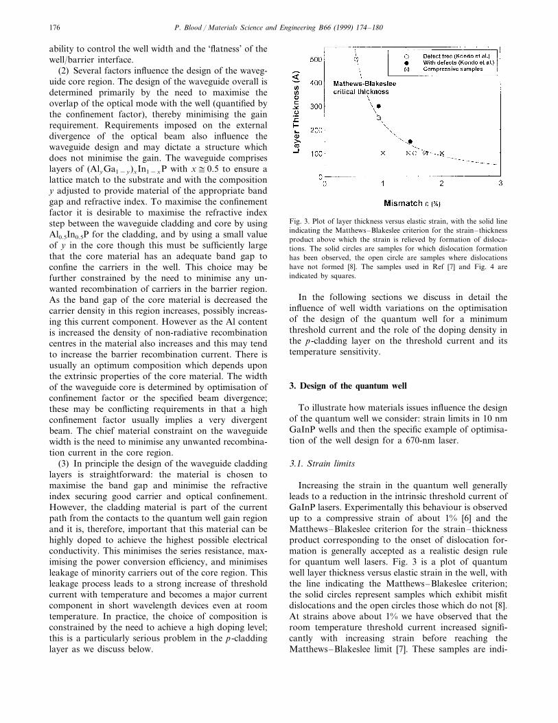
Fig. 3. Plot of layer thickness versus elastic strain, with the solid lineindicating the Matthews–Blakeslee criterion for the strain–thicknessproduct above which the strain is relieved by formation of disloca-tions. The solid circles are samples for which dislocation formationhas been observed, the open circle are samples where dislocationshave not formed [8]. The samples used in Ref [7] and Fig. 4 areindicated by squares.
In the following sections we discuss in detail theinfluence of well width variations on the optimisationof the design of the quantum well for a minimumthreshold current and the role of the doping density inthe p-cladding layer on the threshold current and itstemperature sensitivity.
3. Design of the quantum well
To illustrate how materials issues influence the designof the quantum well we consider: strain limits in 10 nmGaInP wells and then the specific example of optimisa-tion of the well design for a 670-nm laser.
3.1. Strain limits
Increasing the strain in the quantum well generallyleads to a reduction in the intrinsic threshold current ofGaInP lasers. Experimentally this behaviour is observedup to a compressive strain of about 1% [6] and theMatthews–Blakeslee criterion for the strain–thicknessproduct corresponding to the onset of dislocation for-mation is generally accepted as a realistic design rulefor quantum well lasers. Fig. 3 is a plot of quantumwell layer thickness versus elastic strain in the well, withthe line indicating the Matthews–Blakeslee criterion;the solid circles represent samples which exhibit misfitdislocations and the open circles those which do not [8].At strains above about 1% we have observed that theroom temperature threshold current increased signifi-cantly with increasing strain before reaching theMatthews–Blakeslee limit [7]. These samples are indi-
P. Blood / Materials Science and Engineering B66 (1999) 174–180 177
cated by the squares in Fig. 3. Microscopy studiesshowed no evidence for dislocation formation in thesedevices at strains below the Matthews–Blakeslee limit.
To identify the cause of this behaviour the photo-voltage spectra (PVS) [9–11] of laser chips were mea-sured by illuminating the facet with light polarisedparallel and normal to the plane of the well. Thistechnique unambiguously identifies the electron-to-heavy hole (e-hh) and electron-to-light hole (e-lh) tran-sitions in the quantum well. We expect these transitionenergies to decrease with decreasing Ga content due tothe decrease in material band gap, and for the splittingof the (e-hh) and (e-lh) transitions to also increase dueto the concomitant increase in strain. The plot of themeasured splittings as a function of the measured (e-hh)transition energy in Fig. 4 shows that, while there is aninitial increase in splitting with decreasing composition,eventually the splitting decreases even though the tran-sition energies themselves continue to decrease. Thisimplies that while the bandgap of the light-emittingregions continues to decrease, the strain does not corre-spond to that of a homogeneous layer with compositionspecified by the growth calibration. Further TEM stud-ies showed that as the In content is increased (Gadecreased) the strain is partially relieved by the forma-tion of In-rich islands, the so-called Stranski-Krastinovgrowth mode. Although the ‘average’ In content corre-sponds to the intended nominal composition, the quan-tum well material is not homogeneous and thethreshold current increases due to the increased scatter-ing of the guided optical mode by these inhomogenei-ties. Thus the real limits to the acceptable strain are setby the need to maintain a planar growth process rather
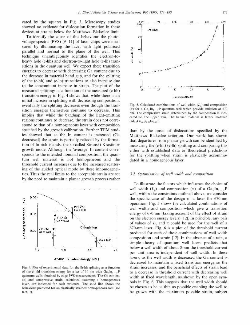
Fig. 5. Calculated combinations of well width (Lz) and composition(x) for a GaxIn1−xP quantum well which provide emission at 670nm. The compressive strain determined by the composition is indi-cated on the upper axis. The barrier material is lattice matched(Al0.5Ga0.5)0.51In0.49P.
than by the onset of dislocations specified by theMatthews–Blakeslee criterion. Our work has shownthat departures from planar growth can be identified bymeasuring the (e-hh) (e-lh) splitting and comparing thiseither with established data or theoretical predictionsfor the splitting when strain is elastically accommo-dated in a homogeneous layer.
3.2. Optimisation of well width and composition
To illustrate the factors which influence the choice ofwell width (Lz) and composition (x) of a GaxIn1−xPwell, within the constraints outlined above, we considerthe specific case of the design of a laser for 670-nmoperation. Fig. 5 shows the calculated combinations ofwell width and composition which give a transitionenergy of 670 nm (taking account of the effect of strainon the electron energy levels) [12]. In principle, any pairof values of Lz and x could be used for the well of a670-nm laser. Fig. 6 is a plot of the threshold currentpredicted for each of these combinations of well widthcomposition and strain [12]. In the absence of strain, asimple theory of quantum well lasers predicts thatbelow a well width of about 8-nm the threshold currentper unit area is independent of well width. In theselasers, as the well width is decreased the Ga content isdecreased to maintain a fixed transition energy so thestrain increases, and the beneficial effects of strain leadto a decrease in threshold current with decreasing wellwidth at fixed wavelength, as shown by the open sym-bols in Fig. 6. This suggests that the well width shouldbe chosen to be as thin as possible enabling the well tobe grown with the maximum possible strain, subject
Fig. 4. Plot of experimental data for the lh-hh splitting as a functionof the el-hhl transition energy for a set of 10 nm wide Gax ln1−xPquantum wells obtained by edge PVS measurements. The Ga content(x) and compressive strain, calculated assuming a homogeneouslayer, are indicated for each structure. The solid line shows thebehaviour predicted for an elastically strained homogeneous well (seeRef. 7).

P. Blood / Materials Science and Engineering B66 (1999) 174–180178
only to the need to maintain planar growth as discussedabove.
Even in the absence of strain, the simple behaviour ofthreshold current with well width is not observed and thethreshold current usually increases with decreasing wellwidth below some optimum value in the region of 6 nm(see [2]). This is due to the effect of lateral variations inthe width of the quantum well (well width fluctuations).Due to inevitable monolayer steps at both well/barrierinterfaces the active region should be treated as a set ofquantum wells of various widths differing by one mono-layer and distributed about the mean value. This leadsto a broadening of the optical gain spectrum which leadsto an increase in threshold current when the spread oftransition energies due to these well width differencesbecomes comparable with and exceeds energy broaden-ing due to intrinsic processes such as thermal broadeningof the emission spectrum and carrier scattering [13]. Wehave included well width fluctuations in our calculationsof threshold current, assuming a Gaussian distributionof well widths with a standard deviation of 1 monolayer.This results in an increase in threshold current at smallvalues of well width, as shown by the closed symbols inFig. 6, leading to a minimum value of threshold as afunction of the well width/composition combination [12].In principle this optimisation process requires knowledgeof the distribution of well widths in a particular growthsystem; in practice the location of the minimum is notparticularly sensitive to the width of the distribution ofwell widths (though the value of threshold current is).The important message is that a minimum in thresholdcurrent as a function of well width exists due to well width
variations and these are often the chief factor determin-ing the choice of well width.
It is common practice to check the transition energyin the well by means of a photoluminescence spectrumrecorded for the grown wafer. However the interpreta-tion of these data is usually based on the assumption thatthe well layer is homogeneous (as discussed above) andthat the growth conditions are such that the activematerial is a true random alloy. It is well known thatGaInP can grow as an ordered structure of alternatinglayers of InP and GaP lying along the (111) planes,resulting in a lower band gap than that of the randomalloy of the same average composition. The presence ofthe ordered phase is best detected by transmissionelectron diffraction and there is evidence that Ramanscattering can also be used for this purpose [14].
4. Waveguide core
The primary consideration in design of the waveguideis the optical confinement factor and far field distributionand there are no direct material constraints (such asmiscibility gaps) in the choice of compositions for theselayers. In the (AlyGa1-y)xIn1−xP alloy the group III togroup V ratio (x) is set to the value giving a lattice matchto the GaAs substrate and the band gap adjusted bychoice of the Al to Ga ratio (y). Consequently, there areno strain-related constraints to the layer thicknesses.
It has been shown that, even in the absence of abottleneck to capture of carriers into the well, there is athermal population of carriers in the barrier/waveguidecore region alongside the well [15] and these may causean increase in the temperature sensitivity of thresholdcurrent. The presence of these carriers does not pose aproblem if they do not recombine in the barrier regionbefore populating the well, though they may contributeto the free carrier optical scattering loss. The carrierconcentration is usually sufficiently low that the contri-bution of intrinsic radiative recombination in the barriersto the total current is very small [15]. The barrier currentcan become important if the barrier material contains asignificant concentration of non-radiative recombinationcentres in the form of deep-state impurities or defects, asis often the case in Al-containing material. It is thoughtthat, as in AlGaAs lasers [16], the non-radiative recom-bination occurs from the indirect X conduction bandminima [17]. However experiments show that carrierleakage over the cladding layer heterobarrier is thedominant thermally activated carrier loss process inAlGaInP devices [15,17] with the usual waveguide widthof about 200 nm. For this reason it has been foundpossible to make lasers with good high-temperaturecharacteristics with barrier compositions as low as 20%Al [18], possibly assisted by a reduction in the concentra-tion of recombination centres as the A1 content isreduced.
Fig. 6. Computed threshold current as a function of well width forthe well width-composition combinations in Fig. 4 which give emis-sion at 670 nm, including the effects of strain. The solid symbolsshow the calculated threshold current including well-width variationsas described in the text, and the calculation shown by open symbolsis for quantum wells of uniform width.

P. Blood / Materials Science and Engineering B66 (1999) 174–180 179
Barrierrecombinationmaybecomeimportant incertainhigh-power, broad-waveguide lasers [19] where the widththe core may be as large as l mm, increasing the barrierrecombination current by a factor 5 over conventionaldevices. The ability to make such devices with goodhigh-temperatureperformancecouldbelimitedbythedeepstate concentration in barrier/waveguide core material.While the deep state concentration can be determined byDLTS measurements [20] (ideally using single layers), thistechnique does not identify the dominant recombinationcentres.Thebestapproachto theoptimisation of thewidthand composition of the core material is probably by asystematic study of the temperature dependence ofthresholdofasetofdeviceswithvariouswaveguidedesigns(rememberingthattheopticalconfinementfactorandhencethe material gain requirement will all vary among the setof lasers). Simulation of device performance using reason-able estimates of the deep state concentration and carrierlifetime are valuable in designing these experiments byindicating the sensitive regions of the parameter space.
5. Waveguide cladding layers
As discussed at the beginning of Section 4, there areno basic constraints to the design of the waveguide coreand cladding regions. The cladding layers usually havea high Al content, and may even comprise AlInP, andare typically 1 mm thick to ensure the guided optical modedoes not penetrate into the narrow gap absorbing regionsbeyond the cladding. However, it has been shown thatthe properties of the cladding layers, particularly thep-cladding, have a major deleterious effect on the temper-ature sensitivity of threshold current [15,17], imposing thechief limitation to the operation of devices at shortwavelength in the region of 635 nm and below. Fig. 7 showsexperimental data for the temperature dependence ofthreshold current for devices of different emission wave-lengths [21].
Thesedifficultiesarisefromtheleakageofminoritycarrierelectrons through the p-cladding layer by the processindicated inthebanddiagraminFig.8.Thethermalenergydistributionofelectronsinthebarrierregionextendsabovethe lowest conduction band edge of the cladding layer(usually the X band) so these electrons are able to leakthrough the cladding layer by diffusion and drift providingahighlytemperaturesensitivecurrentpath.Forgivenlayercompositions, thepotentialbarriercontrolling thiscurrentcan be maximised by use of a highly doped p-claddinglayer so that the hole quasi-Fermi level is as close to thevalence band edge of the cladding layer as possible. Thedoping density of the cladding layer also determines itsconductivity and hence the electric field set up across thecladding by the majority carrier hole current. The senseofthisfieldissuchastoextractelectronsfromthecore/barrierregion and transport them to the p-contact, enhancing
Fig. 7. Experimental data for the temperature dependence ofthreshold current for devices with different composition (strain) in thewell and operating at different wavelength, ranging from 623 nm forthe 0.63% tensile strain device to 664 nm for the 1% compressivestrain device. These data show that the onset of the thermallyactivated increase in threshold current with temperature becomesmore severe at shorter wavelengths [19].
the electron leakage current. Thus the leakage current isvery se2nsitive to the doping density of the p-cladding andthe majority and minority carrier mobilities. The dopingdensity should be as high as possible.
The influence of the doping density of the p-claddinglayer is illustrated by the simulated results for thresholdcurrent as a function of temperature for a 670-nm lasershown in Fig. 9. Full details of the simulation are given
Fig. 8. Simulated energy band diagram of a laser structure nearthreshold illustrating (by arrows) the loss of electrons from the activeregion through the X-conduction band minimum of the p-claddinglayer. Due to the low electrical conductivity of this cladding layer anelectric field is set up in such a sense as to extract electrons from theactive region as a minority carrier drift current. This produces a driftcomponent to the leakage current in addition to the diffusion currentdue to the concentration gradient of the electrons. Efe and Em are theelectron and hole quasi-Fermi levels, respectively.

P. Blood / Materials Science and Engineering B66 (1999) 174–180180
Fig. 9. Simulations of the temperature dependence of thresholdcurrent density of 670 nm quantum well lasers for impurity densitiesin the p-cladding layer ranging from 4×10¹⁷ to 5×1018 cm−3. Thedramatic reduction of the threshold current at high temperatures dueto the increased doping can be seen.
Acknowledgements
Much of the author’s research on AlGaInP lasers hasbeen funded by The Engineering and Physical SciencesResearch Council and has been conducted in collabora-tion with EPI Ltd. The author is especially grateful toSteve Bland of EPI for many valuable discussions onthe issues covered in this paper. Some device structureshave also been grown at the EPSRC Central Facility atthe University of Sheffield. Within the Cardiff team, thework of Paul Mogensen, Peter Smowton and HuwSummers has made major contributions to the ideaspresented in this paper. Paul Hulyer has fabricated allour devices.
References
[1] P.M. Smowton, P. Blood, Visible emitting (AlGa)InP laserdiodes, in: M.O. Manasreh (Ed.), Strained-layer Quantum Wellsand their Applications, Gordon and Breach, 1997, pp. 431–487.
[2] P. Blood, Heterostructures in semiconductor lasers, in: D.V.Morgan, R.H. Williams (Eds.), Physics and Technology of Het-erostructure Devices, Perigrinus, London, 1990.
[3] P.S. Zory Jr (Ed.), Quantum Well Lasers, Academic Press, NewYork, 1993.
[4] L.A. Coldren, S.W. Corzine, Diode Lasers and Photonic Inte-grated Circuits, Wiley, New York, 1995.
[5] D.L. Foulger, P.M. Smowton, P. Blood, P.W. Mawby, IEEProc. Optoelectron. 144 (1997) 23–29.
[6] H.D. Summers, P. Blood, Elec. Letts. 30 (1994) 236–238.[7] P.C. Mogensen, S.A. Hall, P.M. Smowton, U. Bangert, P.
Blood, P. Dawson. IEEE J. Quant. Electron. 34 (1998) 1652–1659.
[8] M. Kondo, K. Domen, C. Anayama, T. Tanahashi, K. Naka-jima, J. Cryst. Growth 107 (1991) 578–582.
[9] P. Blood, Semic. Sci. Technol. 1 (1996) 7–27[10] P. Blood, J.W. Orton, The Electrical Characterisation of Semi-
conductors: Majority Carriers and Electron States, AcademicPress, London, 1992, p. 256.
[11] P.M. Smowton, P. Blood, P.C. Mogensen, D.P. Bour, Int. J.Optoelectron. 10 (1996) 383–391.
[12] P.M. Smowton, H.D. Summers, P. Rees, P. Blood, IEE Proc.Optoelectron. 141 (1994) 136–140.
[13] P. Blood, S. Colak, A.I. Kucharska, IEEE J. Quant. Electron. 24(1988) 1593.
[14] Dunbar, S.A. Hall, Halsall, U. Bangart, 1997, Oxford Mi-croscopy Conference.
[15] P.M. Smowton, P. Blood, IEEE J. Quant. Electron. 31 (1995)2159–2164.
[16] P. Blood, E.D. Fletcher, K.C. Heasman, A.R. Adams, IEEE J.Quant. Electron. 25 (1989) 1459.
[17] D.P. Bour, D.W. Treat, R.L. Thornton, R.S. Geels, D.F. Welch,IEEE J. Quant. Electron. 29 (1993) 1337–1343.
[18] P.M. Smowton, unpublished.[19] L.J. Mawst, A. Bhattacharya, J. Lopez, D. Botez, D.Z. Garbu-
zov, L. DeMarco, J.C. Conolly, M. Jansen, F. Fang, R.F.Nabiev, Appl. Phys. Letts. 69 (1996) 1532–1534.
[20] P. Blood, J.W. Orton, The Electrical Characterisation of Semi-conductors: Majority Carriers and Electron States, AcademicPress, London, 1992, p. 1992.
[21] H.D. Summers, PhD Thesis, University of Wales Cardiff, 1993.
in Ref. [5] and the parameters used give an accuratedescription of experimental data. Material constraintsin AlGaInP have limited the p-doping density using Znto about 5×10⁻⁷ cm−3 and it is clear from the figurethat significant improvements in threshold current andits temperature dependence can be obtained if the dop-ing density is increased to 2×1018 cm−3. The lowsaturation levels for Zn doping of AlGaInP in earlywork were a consequence of non-optimised growthconditions and levels of 1–2×1018 cm−3 are nowpossible. Mg gives higher doping levels but suffers frommemory effects and sensitivity to oxygen, which com-plicates the growth process.
Although it is now possible to achieve doping levelsin excess of 1018 cm−3 the sensitivity of thresholdcurrent to the value of the doping density means that itis important to control this parameter to achieve repro-ducible device performance. This implies that measure-ment of the doping density of the p-cladding isimportant in the manufacture of high performancedevices.
6. Summary
We have reviewed a number of issues in the growthof structures for red-emitting AlGaInP laser diodeswhich have a critical influence on device performance,including strain limits to growth of homogeneous quan-tum wells, lateral well width variations, and the dopingdensity of the p-cladding layer. Control of these factorsis important in achieving reliable production of devices,particularly at the shorter wavelengths accessible withthis material system, and this demands that methods beavailable to monitor these characteristics of the grownstructure. Device simulations can provide valuable in-sight into the effect that these issues have on themeasured performance of devices.