material characterization for composite materials in load
TRANSCRIPT

Air Force Institute of TechnologyAFIT Scholar
Theses and Dissertations Student Graduate Works
3-22-2012
Material Characterization for Composite Materialsin Load Bearing Wave GuidesGabriel Almodovar
Follow this and additional works at: https://scholar.afit.edu/etd
Part of the Structures and Materials Commons
This Thesis is brought to you for free and open access by the Student Graduate Works at AFIT Scholar. It has been accepted for inclusion in Theses andDissertations by an authorized administrator of AFIT Scholar. For more information, please contact [email protected].
Recommended CitationAlmodovar, Gabriel, "Material Characterization for Composite Materials in Load Bearing Wave Guides" (2012). Theses andDissertations. 1027.https://scholar.afit.edu/etd/1027
MATERIAL CHARACTERIZATION FOR COMPOSITE MATERIALS IN LOAD BEARING WAVE GUIDES
THESIS
Gabriel Almodovar, Captain, USAF
AFIT/GAE/ENY/12-M01
DEPARTMENT OF THE AIR FORCE AIR UNIVERSITY
AIR FORCE INSTITUTE OF TECHNOLOGY
Wright-Patterson Air Force Base, Ohio
APPROVED FOR PUBLIC RELEASE; DISTRIBUTION UNLIMITED

The views expressed in this thesis are those of the author and do not reflect the official
policy or position of the United States Air Force, Department of Defense, or the United
States Government. This material is declared a work of the U.S. Government and is not
subject to copyright protection in the United States.
AFIT/GAE/ENY/12-M22
MATERIAL CHARACTERIZATION FOR COMPOSITE MATERIALS IN LOAD BEARING WAVE GUIDES
THESIS
Presented to the Faculty
Department of Aeronautics and Astronautics
Graduate School of Engineering and Management
Air Force Institute of Technology
Air University
Air Education and Training Command
In Partial Fulfillment of the Requirements for the
Degree of Master of Science in Aeronautical Engineering
Gabriel Almodovar, BS
Captain, USAF
March 2012
APPROVED FOR PUBLIC RELEASE; DISTRIBUTION UNLIMITED.

AFIT/GAE/ENY/12-M01
MATERIAL CHARACTERIZATION FOR COMPOSITE MATERIALS IN LOAD BEARING WAVE GUIDES
Gabriel Almodovar, BS Captain, USAF
Approved:
___________________________________ ___________ Dr Anthony Palazotto (Chairman) Date _______________________________________ ___________ Dr Khalid Lafdi (Member) Date _____________________________________ ___________ Maj Milo Hyde USAF (Member) Date

iv
Abstract
This study will establish a methodology to examine samples of composite
material for application in a load bearing waveguide. The composite material will
operate in a specific frequency range for applications in small RPAs. A graphite epoxy
stiffening component will be primarily considered. Different nickel, graphene, and
carbon nanotube (CNT) coatings and films will be applied to the graphite epoxy. Tests
will determine the material's radio frequency (RF) performance for application as an
antenna/waveguide component. The study will use scattering (S) parameters determined
from a network analyzer to collect these data. The S parameters will then be used to
resolve the composites permittivity and reflectivity and allow an estimation of a full scale
waveguides performance made from pretested composite material.

v
Acknowledgements
Throughout this thesis effort, numerous people have given me overwhelming help
and support. My faculty advisor, Dr Anthony Palazotto, helped me through each obstacle I
encountered. A special thanks goes out to Maj Milo Hyde. Without his patience and
knowledge, I would not have been able to complete this work. Dr Khalid Lafdi provided
technical expertise and needed advice. The AFIT laboratory staff always provided me with
the tools, experience, and expertise needed. My fiancée, family, and friends: without them,
this would not be possible. Through the rigorous curriculum, they ensured I stayed
grounded and focused on what truly matters in life. Whether it was weekend trips,
Sunday fundays, loving gestures, support, or just their understanding, I sincerely
appreciate everyone’s help and appreciate all of the time and effort spent on this project.
Finally, I would like to thank all the FOB and deployed service members both home and
abroad…get home safe.
Gabe Almodovar

vi
Table of Contents Page
Abstract .................................................................................................................. iv
Acknowledgements ................................................................................................. v
Table of Contents ................................................................................................... vi
List of Figures ...................................................................................................... viii
List of Tables .......................................................................................................... x
List of Symbols ...................................................................................................... vi
List of Abbreviations ........................................................................................... xiii
I. Introduction ..................................................................................................... 1 1.1 Motivation for research ........................................................................... 2
1.2 What is a waveguide ............................................................................... 3
1.3 Composites .............................................................................................. 5
1.4 SWASS concept ...................................................................................... 8 1.5 CLASS programs .................................................................................... 9 1.6 Thesis Objective.................................................................................... 11
II. Theory ........................................................................................................... 12 2.1 Theory of electromagnetic wave propagation ....................................... 12
2.2 Material classifications and properties.................................................. 15
2.3 Electromagnetic wave propagation and material interaction ................ 18
2.4 Materials under test ............................................................................... 21 2.4.1 Baseline Composite ............................................................................... 22 2.4.2 CNT composite .................................................................................... 23 2.4.3 Ni-coated CNT composite .................................................................... 24 2.4.4 P100 carbon fiber composite ................................................................ 25 2.4.5 Pyrolytic graphite composite ................................................................ 26 2.5 Carbon based material background ....................................................... 27 2.6 Electromagnetic Material Properties Measurements ............................ 32
2.7 Nicholson Ross Weir algorithm and the complex wave equation ........ 36
2.8 Conduction (ohmic) losses ........................................................... 38 2.9 Statistical analysis ...................................................................... 40
2.10 Summary .................................................................................. 41

vii
III. Methodology ............................................................................................. 43 3.1 The low observable (LO) laboratory and support equipment ............... 43 3.2 The network analyzer calibration process ............................................. 43
3.3 Transmission reflection method testing ................................................ 52
3.4 Testing the materials ............................................................................. 54
3.5 Resistivity measurements...................................................................... 56
IV. Results and Analysis ................................ Error! Bookmark not defined.8 4.1 Permittivity from NRW ........................................................................ 58
4.2 Transmission and Reflection coefficients ............................................. 60
4.3 Power coefficients ................................................................................. 63 4.3.1 Brass plate ........................................................................................... 64 4.3.2 Baseline composites ............................................................................ 67 4.3.3 CNT composite ................................................................................... 69 4.3.4 Nickel coated CNT composite ............................................................ 71 4.3.5 P100 carbon fiber composite .............................................................. 73 4.3.6 Pyrolytic graphite ................................................................................ 75 4.4 Power coefficient comparison of the composite materials ................... 76
V. Conclusions and Recommendations ............................................................. 81 5.1 Conclusions ........................................................................................... 81 5.2 Recommendations and suggestions of future work .............................. 81
VI. Bibliography ............................................................................................. 84

viii
List of Figures Page
Figure 1. Hollow rectangular waveguides ......................................................................... 4
Figure 2. Common weave architectures ............................................................................. 7
Figure 3. Slotted waveguide and hat stiffened panel ......................................................... 9
Figure 4. A conceptual SWASS component. ..................................................................... 9
Figure 5. NASA F-18 with embedded MUSTRAP antenna ............................................ 10
Figure 6. Electromagnetic wave in the electric and magnetic components ..................... 14
Figure 7. Bohr's model of a carbon atom ......................................................................... 16
Figure 8. Energy band gap representation ....................................................................... 18
Figure 9. Atom in neutral state and polarized in an electric field .................................... 20
Figure 10. Baseline composite ......................................................................................... 22
Figure 11. CNT composite ............................................................................................... 23
Figure 12. Ni-coated CNT composite .............................................................................. 25
Figure 13. P100 composite .............................................................................................. 26
Figure 14. Pyrolytic graphite composite .......................................................................... 27
Figure 15. A graphene sheet being formed into bucky balls, CNTs, and graphite .......... 28
Figure 16. SWCNTs......................................................................................................... 30
Figure 17. Two-port network with inputs labeled ........................................................... 33
Figure 18. Agilent network analyzer ................................................................................ 34
Figure 19. WR-90 waveguide transmission line .............................................................. 35
Figure 20. Rectangular waveguide dimensions ............................................................... 40
Figure 21. Agilent network analyzer ............................................................................... 43
Figure 22. Brass calibration plater ................................................................................... 44
Figure 23. Coaxial cable connector ................................................................................. 45
Figure 24. Torque wrenchess ........................................................................................... 46
Figure 25. WR-90 waveguide section .............................................................................. 46
Figure 26. Metal mounting plates .................................................................................... 48
Figure 27. Line standard measurement ............................................................................ 50
Figure 28. Thru measurement .......................................................................................... 50
Figure 29. Short measurement ......................................................................................... 51

ix
Figure 30. Test section ...................................................................................................... 52
Figure 31. Baseline composite .......................................................................................... 53
Figure 32. Baseline composite in the test section ............................................................. 54
Figure 33. Baseline composite in testing .......................................................................... 54
Figure 34. P100 fiber in testing......................................................................................... 55
Figure 35. Surface resistivity meter .................................................................................. 56
Figure 36. 4 point probe .................................................................................................... 56
Figure 37. Baseline composite imaginary permittivity (runs 1-5) .................................... 59
Figure 38. Baseline composite permeability (runs 1-5) .................................................... 60
Figure 39. Magnitude of 𝑆21 for the baseline composite (runs 1-5) ................................. 61
Figure 40. Magnitude of 𝑆11 for the baseline composite (runs 1-5) ................................. 62
Figure 41. Transmission and reflection coefficient for one measurement ........................ 63
Figure 42. Power coefficient for the brass plate .............................................................. 64
Figure 43. Power coefficient for the brass plate (magnified) .......................................... 65
Figure 44. Imaginary part of the reflection coefficient .................................................... 66
Figure 45. Power coefficient trend line for the baseline composite ................................ 67
Figure 46. Power coefficient for the CNT composite ...................................................... 68
Figure 47. Power coefficient trend line for the CNT composite ...................................... 69 Error! Bookmark
Figure 48. Power coefficient for the Nickel coated CNT composite ............................... 70
Figure 49. Power coefficient trend line for the Nickel coated CNT composite71Error! Bookmark not defin
Figure 50. Power coefficient for the P100 fiber composite ............................................. 72
Figure 51. Power coefficient trend line for the CNT composite ...................................... 73 Error! Bookmark
Figure 52. Power coefficient for the pyrolitic graphite fiber composite .......................... 74
Figure 53. Power coefficient trend line for the CNT composite ...................................... 75
Figure 54. Power coefficient trend line for the pyrolitic graphite composite .................. 76
Figure 55. Power coefficient trend lines of the composite materials ............................... 77
Figure 56. Power coefficient trend lines of the composite materials ............................... 77
Figure 57. Power coefficient trend line for the CNT composite ...................................... 79

x
List of Tables Table 1. Measured sample thickness 3 .............................. Error! Bookmark not defined.Table 2. Resistivity measurements for the composite materials .................................... 57
Table 3. Frequency versus power coefficients for different materials trend lines ........... 78
Page

xi
List of Symbols Symbol
εo Permittivity of free space
D Electric flux density
t Sample thickness
A Antenna area
R Radar range
𝑃𝑠 Power transmitted
𝜆 Wavelength
𝑃𝑒 Received power
o Target radar cross-section
𝜎 Conductivity
∇ Del operator
𝜌𝑣 Electric charge density per unit volume
E Electric field intensity
B Magnetic field density
H Magnetic field intensity
J Current density per unit area
µ Permeability ε Permittivity
eV Electronvolts
[𝑏𝑖] Network output signal matrix
[𝑎𝑖] Network input signal matrix
a Widest dimension of waveguide opening
b Smallest dimension of waveguide opening
[S] Scatter parameter matrix
𝑺𝒊𝒋 Scatter parameter received at port i and sent from port j (complex number)
Γ Reflection coefficient
𝐾 Specific group of terms used to simplify
Λ Specific group of terms used to simplify

xii
T Transmission coefficient
𝜇𝑟 Relative permeability
𝜀𝑟 Relative permittivity
𝜆𝑐 Cutoff wavelength
𝜆𝑜 Free-space wavelength
c Speed of light
𝑓𝑐 Cutoff frequency
𝜇0 Permeability of free-space
𝛼𝑡 Total attenuation constant
𝛼𝑑 Dielectric attenuation
𝛼𝑐 Conduction (ohmic) losses
𝜂 Intrinsic impedance
𝑅𝑠 Sheet resistivity
𝑓 Frequency
N Sample size
s Standard deviation
𝑋� Sample mean
𝑥𝑖 Specific measurement from a sample set
z Arbitrary representation of any measurement
𝑡𝛼2� Area of the tail end of a T distribution curve
𝑍0 System impedance
𝛿𝑠 Skin depth

xiii
List of Abbreviations Abbreviation
AFIT Air Force Institute of Technology
AFRL Air Force Research Laboratory
DoD Department of Defense
CLAS Conformal Load-bearing Antenna Structure
EM Electromagnetic
ISR Intelligence, Surveillance, and Reconnaissance
SWASS Slotted Waveguide Antenna Stiffened Structure
RPA Remotely Piloted Aircraft
CFRP Carbon Fiber-Reinforced Plastic
eV electronvolts
SAR Synthetic Aperture Radar
DARPA Defense Advanced Research Projects Agency
ISR Intelligence, Surveillance, and Reconnaissance
ISIS Integrated Sensor Is Structure
MUSTRAP Multifunctional Structural Aperture
MWCNT Multi-walled Carbon Nanotube
SWCNT Single-walled Carbon Nanotube
NASA National Aeronautics and Space Administration
CNT Carbon Nanotube
GNR Graphene Nanoribbons
TRM Transmission Reflection Method
NRW Nicolson-Ross-Weir
LO Low Observables
TRL Thru-Reflect-Line
RF Radio Frequency
dB Decibels
Np Nepers
GHz Gigahertz
1
MATERIAL CHARACTERIZATION FOR COMPOSITE MATERIALS IN
LOAD BEARING WAVE GUIDES
I. Introduction
The Department of Defense (DoD) and United States intelligence agencies have
increasingly depended on the electromagnetic spectrum to conduct combat and
intelligence operations. Antenna arrays are important tool for communications and
Intelligence, Surveillance, and Reconnaissance (ISR). These assets are in high demand
because the military and analysts depend on the images, video, voice, and radar data
these assets provide. These antenna components add significant weight and cost in
procurement and operation to these assets. Thus, the aerospace industry has looked at
using composite materials to form multifunctional components, i.e., components capable
of meeting multiple requirements, to cut down on costs. One such concept is a conformal
load-bearing antenna structure (CLAS). The purpose of a CLAS is to perform the
function of both a support structure, capable of taking loads, and an antenna, capable of
transmitting/receiving electromagnetic (EM) waves. One such project is under way at the
Air Force Research Lab (AFRL) in which a hat stiffener support on aircraft skin panels is
combined with a slotted waveguide. This program is called the Slotted Waveguide
Antenna Stiffened Structure (SWASS). This research will look into the feasibility and
performance of carbon based materials and composites in waveguide applications with
the goal of finding composites capable of adequately performing the waveguide function.
The purpose is to establish procedures for developing methods to evaluate alternative
materials for use as lightweight load carrying composite waveguides.

2
1.1 Motivation for research
The increased need for persistent ISR assets and the future fiscal constraints
requires aerospace systems to operate more functions more efficiently. In addition, there
has been a dramatic increase in remotely piloted vehicles (RPAs), and are being designed
to be lighter and more capable. The SWASS can provide aerospace assets with the
ability to accomplish their mission more efficiently. Many aerospace systems have been
designed in such a way that one component achieves one function. This is because of the
difficulty in designing multifunctional components that often times have competing
requirements.
Today's military systems posses increasingly sophisticated radar systems. These
radar systems and antenna are part of a system of systems. For many aircraft, antenna
components must be integrated in the platform by adding an additional housing outside
the desired aerodynamic shape of the aircraft. These additional components pose not
only a weight penalty but can significantly add drag, both of which drive up the cost of
maintaining and operating the aircraft. A SWASS system could reduce or eliminate the
need of an additional housing for the radar antenna components. This will increase the
overall system efficiency by requiring less weight and a smaller total area for the radar
components. [18] The potential for weight savings, increased capability, and the resulting
reduction in life cycle cost are primary reasons for pursuing such multi-functional
designs.

3
Integrating antenna waveguides and skin structure could increase the overall
radar's performance by increasing the antenna area. Equation (1) is the radar range
equation. From this, we can determine that a two fold increase in the frontal area of the
antenna, A, would improve the range, R, by 41% while doubling the transmitted
power,𝑃𝑠, only increases the range by 19%. [18]
𝑅 = �𝑃𝑠𝜋2𝐴2𝑜4𝜋3𝑃𝑒𝜆2
4 (1)
On today's battlefield, combatant commanders demand the data ISR and radar
assets provide. This demand has placed added stress on the low-density assets currently
in the inventory. While these assets provide the needed info, future platforms will be
required to provide more data and capabilities. With the current fiscal realities, future
systems must be able to do more with less.
1.2 What is a Waveguide
A waveguide is a device used to transmit electromagnetic waves (or other types of
waves) from one point to another. The waveguide acts as a conduit for this
electromagnetic energy to travel through. A common type of waveguides is a hollow
metal pipe used to carry electromagnetic waves, primarily radio frequency wave. [19]
This is not the only type of waveguide. A fiber optic cable is a type of waveguide as is
the coaxial cable connected to most television sets. Figure 1 shows a rectangular hollow
waveguide with a 2.286 by 1.016 cm (.9" by .4") opening.

4
Figure 1: Hollow rectangular waveguides
The idea of the waveguide is for electromagnetic waves to enter one end and
propagate to the other end of the waveguide with little or no loss in power. The
waveguide works by reflecting the wave energy, which enters the guide, along the walls.
There is a geometric relationship to what frequencies can enter and, therefore, propagate
inside the waveguide based on the physical size of the waveguide opening. The
frequency range is determined by its shape and dimension. Also, the inside lining
material of the waveguide determines how efficiently it can transmit the electromagnetic
energy. The inside material is responsible for reflecting the electromagnetic energy.
Much like the way a bathroom mirror reflects light waves, the inside material ideally
reflects the radio frequency (RF) waves. Depending on the inside material, it may resist
and absorb much of the energy (create losses). This is very important in designing
waveguides and waveguide structure and will be discussed in later chapters.

5
1.3 Composites
In early Egyptian times, straw and mud were combined and used to build housing.
This early composite was unique because it combined two separate materials who
themselves posses unique material properties. When put together, the “new” composite
material was still made of two distinct materials, but their material properties combined
to produce collective properties not achievable by either material alone. A composite is
simply a "solid material which is composed of two or more substances having different
physical characteristics and in which each substance retains its identity while contributing
desirable properties to the whole." [20] Since a composite is made of two or more
substances, it often times is difficult to characterize a composite's properties because by
definition they are not homogeneous materials.
One class of composites is fiber-reinforced materials. Fiber reinforced
composites consist of high strength fibers bonded to a matrix with distinct boundaries
between them. The fibers are generally the load carrying members, while the
surrounding matrix keeps them in the desired location and orientation. [8] This thesis will
specifically examine carbon fiber-reinforced plastic (CFRP) composite materials.
There are several advantages to using CFRPs. The first and most well known is
the high strength to weight ratio. Composites offer a greater strength to weight ratio than
metals. For instance, Ti-6A1-4V titanium alloy has a tensile strength to weight ratio of
20.1 ∗ 103m compared to 101.9 ∗ 103m for a high strength carbon fiber epoxy, a
fivefold increase. (Do note that these measurements are taken in the direction of the
fiber.)

6
In fiber-reinforced composites, the mechanical properties strongly depend on the
direction of the measurement because by definition composites are not isotropic
materials. Because of the anisotropic nature of fiber-reinforced composites, the
properties can be adapted according to design requirements. Metals on the other hand,
are isotropic materials, and therefore, exhibit equal or nearly equal properties
independent of the direction of measurement. [8] Impact strength, coefficient of thermal
expansion, thermal conductivity, and others also depend on the direction at which they
are measured.
Fiber composites have lower coefficient of thermal expansion than metals. This
means a composite structure may exhibit a better dimensional stability over a wide
temperature range. When using a composite with a metal, note that thermal stresses may
result due to the differences in their thermal expansions. Fiber composites offer high
internal damping, which leads to better "vibrational energy absorption within the material
and results in reduced transmission of noise and vibrations to neighboring structures." [8]
This is desirable in applications where noise and vibrations are issues. Another important
advantage of composites is their non-corroding behavior. However, they can absorb
moisture, which can create internal stresses. Composites are normally coated or painted
to prevent moisture absorption.
Composites first started seeing use in military aircraft in 1969 as a boron fiber
reinforced epoxy skin in F-14 horizontal stabilizers. [8] Since then, fiber-reinforced
composites have seen a steady increase. The F-22 contains approximately 25% by
weight of carbon fiber-reinforced composites, and the future Boeing 787 Dreamliner is
expected to have about 50% by weight of composites. The steady rise of composite
7
components in aircraft is due to all the conducted research, the millions of flight hours
parts have accumulated, and overall better understanding of them. This has led to an
increase in confidence in a fiber-reinforced composite's structural integrity and durability.
With an increased understanding of composites, you can begin to develop multifunctional
components, such as a SWASS system. Such work aims to integrate the electromagnetic
functionality into lightweight host structures and materials. [21]
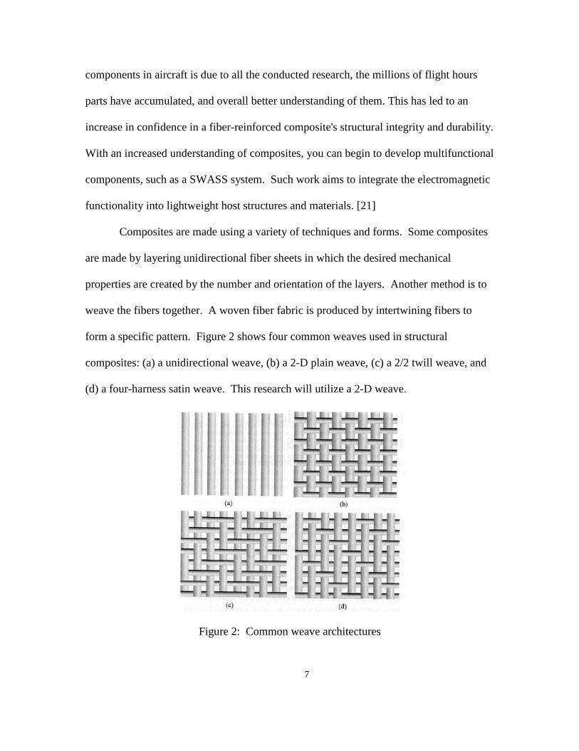
Composites are made using a variety of techniques and forms. Some composites
are made by layering unidirectional fiber sheets in which the desired mechanical
properties are created by the number and orientation of the layers. Another method is to
weave the fibers together. A woven fiber fabric is produced by intertwining fibers to
form a specific pattern. Figure 2 shows four common weaves used in structural
composites: (a) a unidirectional weave, (b) a 2-D plain weave, (c) a 2/2 twill weave, and
(d) a four-harness satin weave. This research will utilize a 2-D weave.
Figure 2: Common weave architectures

8
The choice of weave does effect the electromagnetic properties of the composite
being designed. "The broadband EM properties are sensitive in the choice in fiber type,
weave, bundle size, and bulk dielectric properties of the resin." [1] Research is being
conducted to try to model not only a composite's mechanical properties but also its EM
properties. "By tailoring the EM properties of structural composites (e.g., complex
permittivity and permeability) it may be possible to integrate antennas, frequency
selective surfaces, and other electromagnetic components directly into structural skin of
future commercial and military vehicles and structures." [1] While this thesis does not
analyze the effects and changes in EM properties from different weaves, fibers, and
resins, it is important to note that these can greatly affect the EM properties of the
composite. This research will however analyze the effects of different coating, films, and
additives.
1.4 The SWASS Concept
The Slotted Waveguide Antenna Stiffened Structure program focuses on
combining aircraft skin support structure with a slotted waveguide. A slotted waveguide
differs from a regular hollow rectangular waveguide in that it is designed with slots on
one side of the waveguide. As the EM energy travels down the waveguide, the slots are
designed to allow the EM energy to escape or emit, in the case of this research RF
energy. The SWASS concept aims to combine a slotted waveguide and a hat-stiffened
panel. The hat-stiffened panel is designed to create a panel capable of handling the
expected mechanical loads while minimizing weight and materials. Figure 3 shows a
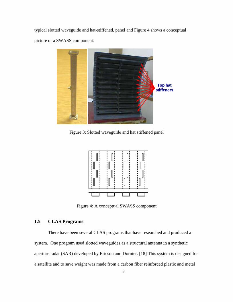
9
typical slotted waveguide and hat-stiffened, panel and Figure 4 shows a conceptual
picture of a SWASS component.
Figure 3: Slotted waveguide and hat stiffened panel
Figure 4: A conceptual SWASS component
1.5 CLAS Programs
There have been several CLAS programs that have researched and produced a
system. One program used slotted waveguides as a structural antenna in a synthetic
aperture radar (SAR) developed by Ericson and Dornier. [18] This system is designed for
a satellite and to save weight was made from a carbon fiber reinforced plastic and metal
Top hat stiffenersTop hat
stiffeners

10
lining. The system was required to support its own weight when in the fully deployed
configuration.
The Defense Advanced Research Program Agency (DARPA) has a program
called the Integrated Sensor is Structure (ISIS). This program aims to "develop the
technologies that enable extremely large lightweight phased-array radar antennas to be
integrated into an airship platform." [21] This system is currently in design with an
expected demonstration in 2013/14 timeframe.
The multifunction structural aperture (MUSTRAP) program structurally
embedded an antenna in the vertical stabilizer of a NASA F-18, as shown in Figure 5.
Figure 5: NASA F-18 with embedded MUSTRAP antenna
The program successfully flight tested the antenna and showed that it increased the radar
performance by 15 to 25 dB because of the increase in the overall antenna size. [22]
There are significant benefits to load bearing sensors and antenna that can
increase the efficiency of different platforms, and work continues to be done to develop
these technologies.
11
1.6 Thesis Objective
The objective of this thesis is to establish a methodology to examine samples of
composite material for application in a load bearing waveguide. The composite material
will operate in the X band frequency range for applications in small RPAs. A graphite
epoxy stiffening component will be considered with different carbon based coatings and
films. Measurements will be performed to characterize the electrical properties of the
composite. These measurements will collect scatter (S) parameter information using a
network analyzer. The S parameters data will then be used to resolve the composites
permittivity and reflectivity and allow an estimation of a full-scale waveguides
performance made from pretested composite material.

12
II. Theory
The purpose of this chapter is to describe and understand some key principles that
effect how a material reacts to applied electromagnetic (EM) energy. First, a brief
introduction to electromagnetic theory and Maxwell's equations will be presented. This
will outline the governing equations for EM waves themselves and serve as the basis for
developing much of the theory to be presented. Then the chapter will cover the different
material classifications, and the theory affecting a material's electrical properties. Next,
the chapter will briefly describe the materials to be tested. This is followed by
background information on the atomic structure and makeup of different carbon based
materials and how it relates to its electrical properties. Lastly, a discussion of the theory
pertaining to the test methods and algorithms used to characterize the material’s
reflectivity, conductivity, permittivity, and other electrical properties will be presented.
The experiments required for determining a material’s suitability in a waveguide
application requires a basic understanding of material, electromagnetic, and physics
principles.
2.1 Theory of Electromagnetic Wave Propagation
“The relations and variations of the electric and magnetic fields, charges, and
currents associated with electromagnetic waves are governed by physical laws, which are
known as Maxwell’s equations.” [6] Maxwell’s equations describe, macroscopically, the
connection between the electric field and electric charge, magnetic field and electric
current, and the bilateral coupling between the electric and magnetic field quantities. [23]

13
These equations hold true for all materials, including free space, and at any (x,y,z)
location. The general forms of Maxwell’s equations are:
∇ ∗ 𝐷 = 𝜌𝑣 (1)
∇ × 𝐸 = −𝜕𝐵𝜕𝑡
(2)
∇ ∗ 𝐵 = 0 (3)
∇ × 𝐻 = 𝐽 + 𝜕𝐷𝜕𝑡
(4)
where
E = electric field intensity
D = electric flux density
and D = ε E, where ε = electrical permittivity of the medium
H = magnetic field intensity
B = magnetic flux density
And B = µ H, where µ =magnetic permeability of the medium
νρ = electric charge density per unit volume
J = current density per unit area
∇ = del operator
The electric flux density, D, is a measure of the strength of an electric field generated by
a free electric charge. The Electric field intensity, E, is a measure for how strong an
electric field is. The magnetic flux density, B, and magnetic field intensity, H, are the
same as the electric flux density and electric field intensity but for the magnetic
component of the EM wave. The current density per unit area, J, is just that. It is the

14
amount of current per unit area just as the electric charge density per unit volume, 𝜌𝑣, is
the amount of electrical charge per unit volume. [23] The del operator,∇, can represent
the gradient of a scalar field, the divergence of a vector field, or the curl of a vector field,
depending on the application.
Maxwell’s equations (1-4) explain the relationship between the electric and
magnetic components of propagating waves. Figure 6 shows a graphical relationship
between the electric and magnetic components described in Maxwell’s equations.
Figure 6: Electromagnetic wave in the electric and magnetic components
The electric and magnetic components impart energy onto any material but the effects of
the EM energy depend on the type of material.

15
2.2 Material Classifications and Properties
Materials are classified according to their reaction to the electric and magnetic
components described in Maxwell’s equations, and the parameters that effect the
propagation of EM waves through a material includes:
𝜎, material conductivity
𝜀, material permittivity
𝜇, material permeability
Conductivity is a measure of a materials ability to allow electric current to flow a
material. Permittivity is a measure of a materials resistance to forming an electric field in
the material (a low permittivity is desired for use in as the inside lining of a waveguide).
Permeability is similar to permittivity. It measures a material’s resistance to the magnetic
field component of EM waves.
The materials can be categorized based on the magnitudes of their conductivities.
The material classifications are conductors, semiconductors, and insulators (dielectrics).
For example, a perfect electrical conductor is described as a material with no resistance to
electric flows, σ = ∞. Conductors allow “free” or “lose” electrons to move throughout
the material such that the net current is zero. A perfect insulator does not allow any
electric flow through the material, σ = 0. At times in this thesis, semiconductors and
insulators will be categorized together because conductors exhibit the desired electrical
properties as opposed to semiconductors and insulators. A material’s category depends
on certain characteristics at the microscopic/atomic level.
Atoms “consist of a very small but massive nucleus that is surrounded by
negatively charged electrons revolving about the nucleus and exert forces of attraction on

16
the positive charges of the nucleus.” [6] These electrons exist in various shells or bands.
Figure 7 shows a simple Bohr’s model for a carbon atom in which the first band is
referred to as the S band while the second band is referred to as the P band. Each
material has a different arrangement and number of electrons that are located throughout
the various bands not mentioned here, but each band can only have a certain maximum
number of electrons.
Figure 7: Bohr’s model of a carbon atom
These bands represent different discrete energy levels. Bohr’s model of an atom
states that electrons can only exist in energy states that are determined by the radii of
their orbital shells. The electron can change its energy band with the absorption or
radiation of energy. This holds true in molecules, the minimum collection of atoms
needed to form a specific material. In molecules, the process becomes a little more
complex because of chemical bonds between the atoms but nonetheless still follow this
idea.

17
The microscopic physical principals for the electrical properties of a material are
“mainly determined by the electron energy bands of the material” [5] The energy gap
between the valence and conduction band determines which classification a material falls
into. The energy gap depends on the atomic structure and makeup of the atoms. The
valence band is the atom’s outer most band that contains electrons at zero degrees Kelvin.
The conduction band is the discrete energy level at which an electron is “free” from the
atomic forces of the nucleus/atom and free to flow throughout the lattice. It is at a higher
energy level than the valence band. These two bands are separated by a gap referred to as
the forbidden gap.
The primary difference between insulators, semiconductors, and conductors is the
amount of energy required for an electron in the valence band to move to the conduction
band. The larger the gap the more energy needed. Insulators have an energy gap greater
than approximately 5 electronvolts (eV) compared to approximately 1eV for
semiconductors and 0 eV for conductors. For instance, the valence and conductions
bands overlap in conductors allowing electrons to become loose from their original atom
with little or no energy. Figure 8 below shows a representation of the three types of
materials.
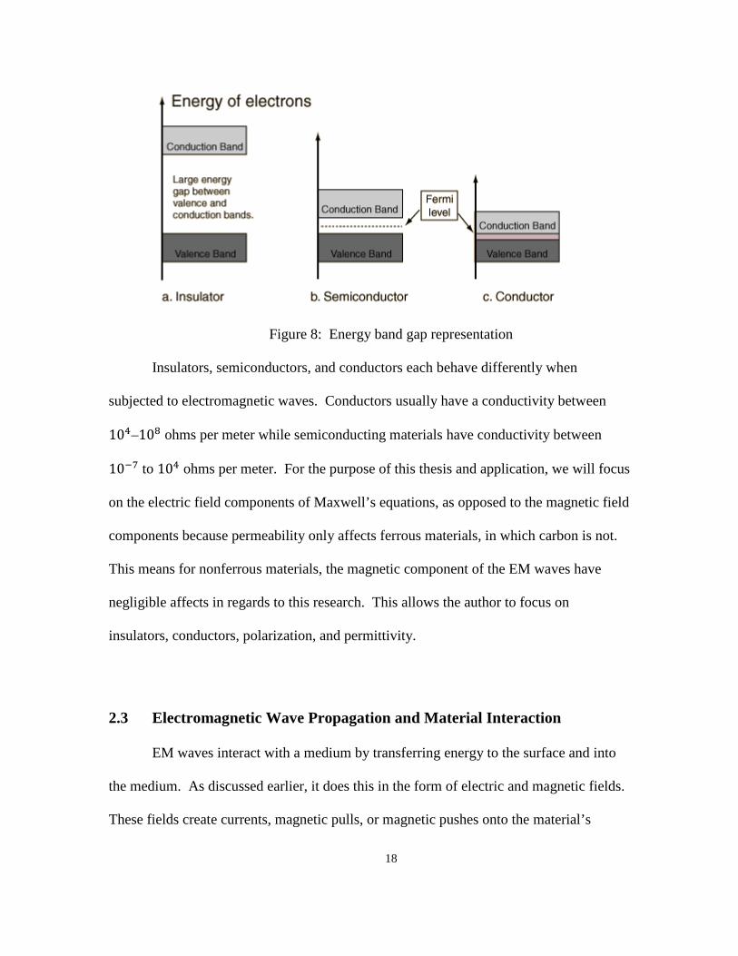
18
Figure 8: Energy band gap representation
Insulators, semiconductors, and conductors each behave differently when
subjected to electromagnetic waves. Conductors usually have a conductivity between
104–108 ohms per meter while semiconducting materials have conductivity between
10−7 to 104 ohms per meter. For the purpose of this thesis and application, we will focus
on the electric field components of Maxwell’s equations, as opposed to the magnetic field
components because permeability only affects ferrous materials, in which carbon is not.
This means for nonferrous materials, the magnetic component of the EM waves have
negligible affects in regards to this research. This allows the author to focus on
insulators, conductors, polarization, and permittivity.
2.3 Electromagnetic Wave Propagation and Material Interaction
EM waves interact with a medium by transferring energy to the surface and into
the medium. As discussed earlier, it does this in the form of electric and magnetic fields.
These fields create currents, magnetic pulls, or magnetic pushes onto the material’s

19
atomic structure and the internal protons and electrons. The additional energy from EM
waves excites the electrons allowing them to potentially jump into higher energy bands or
change their position relative to the nucleus. In addition, the EM waves create a time
dependent alternating magnetic force on the material. The effects of the electric and
magnetic forces depend on the type of material it is acting on.
When a material is subjected to an EM wave, the wave tries to create a current in
the material. In a metals (conductor), there is very little resistivity to the generated
current because metals have electrons that require little or no energy to become free
electrons. The free electrons consolidate at the surface of the material and collectively
oscillate as the EM wave propagates. This movement of electron creates a conduction
current in the material. As described in Maxwell’s equations, this current in turn
generates a similar EM wave that propagates further down the material. In reality, some
energy is lost in the form of heat in all materials, but ideally, the energy from the input
EM wave is not wasted as heat. Instead, the energy is used to generate a current that
(ideally) flows without resistance that then generates the same EM wave. Since most
metals have very low resistivity, and the EM wave propagates along the surface.
In dielectric materials (insulators), the EM wave has a different effect because of
how the material reacts to the applied energy/force. The nucleus and electrons require
more energy to separate because the forbidden gap separating them is larger than in
metals. Some of the electrons may become free from the EM wave energy but not all of
them will. While the EM waves may not have enough energy to produce very many free
electrons, the electric (and potentially magnetic) fields distort the atoms in the material.
If we consider the nucleus of an atom to be fixed, the forces from the electric field will

20
alter the concentration of where the electrons will position themselves. This polarizes the
atom as depicted in Figure 9.
Figure 9: Atom in neutral state and polarized in an electric field
The distorted electrons can return to the original position once the applied EM field is
removed, similar to a stretched spring. The energy to “stretch” the atom is stored and
then released back in the form of energy once external forces are removed. This storage
of energy is the principle behind capacitors, and permittivity quantifies this polarization.
This polarization is also referred to as a displacement current. Another way to describe a
good conductor is that its conduction current is significantly greater than the
displacement current.
As discussed in previous sections, a materials reaction to the electric and
magnetic field is quantified by the material parameters permittivity and permeability,

21
respectfully. While the atomic structure and forbidden gap play an important role in a
material’s response to EM waves, they do not dictate how a material will react under all
circumstances. Permittivity, permeability, and conductance are also temperature and
frequency dependent. The purpose of this study is to test carbon-based materials for their
permittivity in the X-band frequency range at room temperature.
2.4 Materials under test
The focus of this research is to examine different coating, films, and materials to
improve the electrical properties of composites. Previous research focused on
mechanical properties of a slotted waveguide structure made of a composite. The
composite was a resin reinforced plain-woven carbon fiber fabric made from Grafil 34-
700 fibers and RS-36 epoxy resin. While the material performed adequately from a
structural standpoint, it left much to be desired in terms of its electrical properties.
In this research, Grafil 34-700 fibers will be the fiber material. Due to logistical issues,
the composites will use EPON 862 epoxy instead of the RS-36.
Grafil 34-700 is a carbon fiber with a tensile strength of 2572 MPa and a modulus
of 137 GPa. The EPON 862epoxy resin is a low viscosity liquid epoxy resin. [27] All the
materials will be made of a Grafil 34-700 2-D plain weave infused with the EPON 862
epoxy resin cured in an auto clave. The autoclave is a pressure vessel that subjects the
composite to high pressure and temperature. This allows the resin and fiber fuse
together. This process produces more consistent and better composites by reducing the
voids within the resin and fiber.

22
The autoclave cured all the composites at .55 MPa (80 psi) and 121 degrees
Celsius (250 Fahrenheit) for two hours followed by four hours at .55 MPa and 177
degrees Celsius (350 Fahrenheit) to complete the process. From this process, five
different composites are manufactured: baseline composite, carbon nanotubes (CNTs)
composite, nickel (Ni) coated CNTs composite, P100 fiber composite, and pyrolitic
graphite composites. These are described in further detail in following sections.
.
2.4.1 Baseline composite
The baseline carbon fiber composite is the Grafil 34-700 two-dimensional fiber
weave fabric and the EPON 862 epoxy resin. The Grafil fiber weave and EPON epoxy
are infused at a 50/50 weight fraction. Figure 10 shows the baseline composite.
Figure 10: Baseline composite
The resin is layered into a film in order to regulate the amount of resin. The layer of resin
is sandwiched with one ply of the fiber weave and is cured in the autoclave. This same
process is similarly repeated for the other composites.

23
2.4.2 CNT Composite
For this composite, CNTs (more specifically carbon nanofibers) are mixed into
the resin prior to infusing with the Grafil weave. The CNTs are approximately 60
nanometers (nm) in diameter and 1000nm in length. Figure 11 shows the CNT
composite.
Figure 11: CNT composite
The CNT composite is made of 4% CNT, 46% resin, and 50% fiber weave by weight
fraction. The CNTs are mixed into the resin uniformly using a paint mill to mix and layer
into a film. The CNTs themselves are made from a process called chemical vapor
disposition (CVD). The CVD process works to produce thin films or layers of high
purity materials by chemical reaction of precursors and reactants. The CVD process is
well understood and literature on the process is readily available. Each CVD process
follows the same process but may differ in their “recipes.” Specific information on the

24
CVD process used to produce the CNTs used in this research will not be discussed in
additional detail.
The addition of CNTs in the composite is expected to improve both the
mechanical and electrical properties. While this thesis will not determine the change
mechanical properties of the tested materials, studies have been conducted to determine
the effects of CNTs dispersed into resins. “The dispersion of the multi-walled CNTs in
epoxy resin influences its strengthening effect,” but also research has seen different
composites “becoming more brittle with the incorporation of CNTs.” [28] [29] Research
has shown quality, type, size, resin, etc can change how the addition of CNTs affect the
composites performance. Similar research shows this holds true for the electrical
properties. Additional discussions on the electrical properties of carbon-based materials
are in further sections.
2.4.3 Nickel Coated CNT Composite
Similarly as the CNT composite, Ni-coated CNTs are mixed in the resin before being
infused to the fiber weave via the autoclave. The same CNTs go through a specific
process to coat them with nickel. The process includes conditioning the CNTs in
different solutions and adding reactants and precursors to produce the nickel coating.
The thickness of the coating is regulated by the timing and chemical reactions among
other things. The Ni-coated CNTs are mixed with the resin and the fiber weave in the
same manner and ratio as the CNT composite. The CNTs in this research are coated with
30nm of nickel. Figure 12 shows the Ni-coated CNT composite.

25
Figure 12: Ni-coated CNT composite
Similarly, the specific process used to coat the CNTs will not be discussed in any
more detail. The nickel coating process information is proprietary.
2.4.4 P100 Carbon Fiber Composite
The P100 carbon fiber is commercially produced mesophase pitch high
conductive fiber by a company called Amoco. Mesophase pitch describes the precursor
used to create the continuous carbon fibers. This process works by melting down the
mesophase pitch precursor into a thick liquid. The liquid is sprayed out of spinning jets
where it is stretched to align the molecules in a fiber and remove voids. This fiber is
subject to various gasses and temperatures. At the end of the process, the pitch (usually
coal or oil based) is ultimately replaced with only carbon elements (carbon or graphite)

26
then surface treated. This is one of several ways to make carbon fiber. More information
on the mesophase pitch process is available in published literature.
For the P100 fiber, not much public information is available. The fiber has a
ultimate tensile strength of 970 MPa, tensile modulus of 470 GPa, and a density of 1.8
grams per cubic centimeter. The P100 fibers did not come in an already woven fabric.
Instead, the fibers come as individual loose strands. To incorporate the fibers into the
composite, they were hand aligned on a sheet of resin. The P100 fiber and EPON epoxy
combined weight fraction was 50% of total weight. Figure 13 shows the P100
Composite.
Figure 13: P100 Composite
2.4.5 Pyrolitic Graphite Composite
Pyrolitic graphite is highly aligned graphite produced using the CVD method. A
substrate is subjected to precursors and reactants under high temperature and pressure. The
pyrolitic graphite was made at 2200 degrees Celsius and a pressure of 133 Pa (1 torr). In the
process, carbon is slowly deposited in thin layers across a substrate. The process is repeated

27
until the desired thickness is achieved. Once the pyrolitic graphite was produced, the EPON
resin was used to adhere it to composite. Figure 14 is the pyrolitic graphite composite.
Figure 14: Pyrolitic graphite composite
Carbon based materials and the theory that effect their materials properties will be further
discussed in the next sections. The purpose of this section was to introduce the materials.
2.5 Carbon based materials background
The inside material of rectangular hollow waveguides are almost extensively
made of metals. The metals have a high conductivity and results in a very low energy
loss as the wave propagates through the waveguide. This research focuses on alternative
materials that would allow the waveguide to perform its function with minimal drop in
performance. This section will describe different types of carbon based crystalline forms.
Graphene is “a planar allotrope of carbon where all the carbon atoms form
covalent bonds in a single plane.” [7] Allotropes are elements made of the same atoms as
each other that are structurally bonded differently. A single plane graphene can be used
28
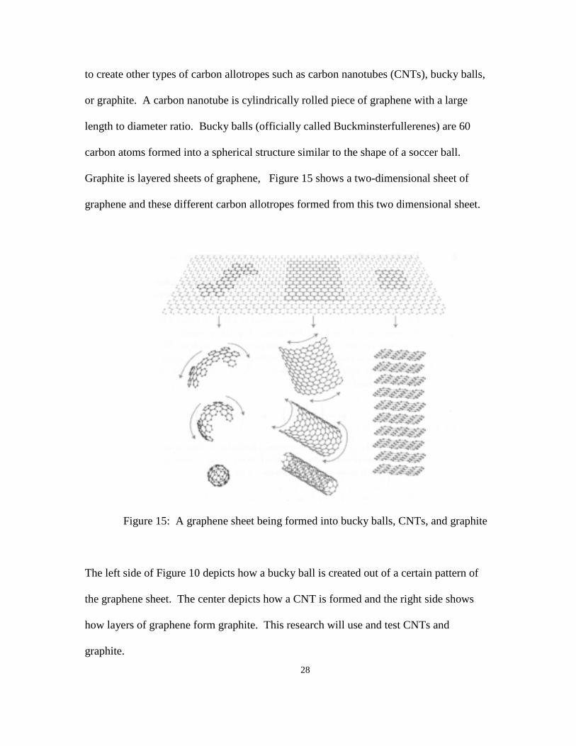
to create other types of carbon allotropes such as carbon nanotubes (CNTs), bucky balls,
or graphite. A carbon nanotube is cylindrically rolled piece of graphene with a large
length to diameter ratio. Bucky balls (officially called Buckminsterfullerenes) are 60
carbon atoms formed into a spherical structure similar to the shape of a soccer ball.
Graphite is layered sheets of graphene, Figure 15 shows a two-dimensional sheet of
graphene and these different carbon allotropes formed from this two dimensional sheet.
Figure 15: A graphene sheet being formed into bucky balls, CNTs, and graphite
The left side of Figure 10 depicts how a bucky ball is created out of a certain pattern of
the graphene sheet. The center depicts how a CNT is formed and the right side shows
how layers of graphene form graphite. This research will use and test CNTs and
graphite.

29
Since graphene can be used to form other carbon allotropes, it is important to
have a basic understanding of is atomic structure. A single carbon atom naturally has
four valence electrons located in its second band, the P band. In graphene, the valence
electrons from the carbon atoms will form three covalent bonds with neighboring carbon
atoms and have the “electrons localized along the plane connecting carbon atoms.” [7]
These types of bonds are strong and responsible for the great strength and mechanical
properties of graphene and CNTs. Normal to the plane or sheet formed by the carbon
atoms, a much weaker type of covalent bonds is formed. Essentially, in a 2-D sheet of
graphene, the carbon atoms in the same plane (the sheet) are strongly bonded together.
These bonds do not require all the valence electrons. Therefore, the remaining electrons
are loosely held normal the sheet. This is where the “electron cloud is distributed normal
to the plane connecting atoms.” [7] The electrons in these bonds are “weakly bound to the
nuclei and, hence, are relatively delocalized.[7] These delocalized electrons are the ones
responsible for the electronic properties of graphene and CNTs.” [7] The delocalized
electrons can become free electrons with little additional energy. The great mechanical
strength of the carbon bonds and the delocalized electrons is what makes these carbon
based materials warrant consideration for application in load bearing composite
waveguides. They show the potential to handle the mechanical strength at lighter weight
and posses the desired electrical properties (conductivity and permittivity).
CNTs can come in different types, and we will now distinguish them as either a
single-walled carbon nanotube (SWCNT), a multi-walled carbon nanotube (MWCNT), or
a graphene nanoribbon (GNR). A SWCNT is a hollow cylindrical structure of carbon
atoms with a diameter that ranges from about .5 to 5 nm and lengths of the order of

30
micrometers to centimeters. A MWCNT is similar in structure to SWCNT but has
multiple nested or concentric cylindrical walls with the spacing between the walls
comparable to the interlayer spacing in graphite, approximately 0.34 nm.” [7] For the
different types of CNTs, we will focus on the electronic band structure derived from the
band structure of graphene. This will give insight into the properties and performance of
CNT devices. GNRs are discussed in more detail later in this chapter.
Chirality is an important concept used to “identify and describe different
configuration of CNTs and their resulting electronic band structure.” [7] A chiral object is
an object whose mirror image is not superimposable onto itself. Objects whose mirror
object can be superimposed onto its self are called achiral. All SWCNTs fall into one of
these categories, which are broken down into further sub-categories. The physical
structure of SWCNTs fall into either chiral, armchair, or zigzag lattice structure as
depicted in Figure 16. The SWCNTs in Figure 16b and 16c, are achiral.
Figure 16: SWCNTs - (a) A chiral CNT, (b) armchair CNT, and (c) a zigzag CNT
31
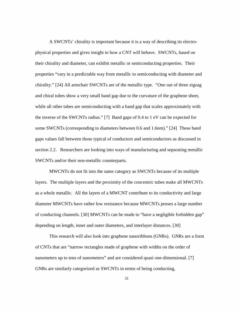
A SWCNTs’ chirality is important because it is a way of describing its electro-
physical properties and gives insight to how a CNT will behave. SWCNTs, based on
their chirality and diameter, can exhibit metallic or semiconducting properties. Their
properties “vary in a predictable way from metallic to semiconducting with diameter and
chirality.” [24] All armchair SWCNTs are of the metallic type. “One out of three zigzag
and chiral tubes show a very small band gap due to the curvature of the graphene sheet,
while all other tubes are semiconducting with a band gap that scales approximately with
the inverse of the SWCNTs radius.” [7] Band gaps of 0.4 to 1 eV can be expected for
some SWCNTs (corresponding to diameters between 0.6 and 1.6nm).” [24] These band
gaps values fall between those typical of conductors and semiconductors as discussed in
section 2.2. Researchers are looking into ways of manufacturing and separating metallic
SWCNTs and/or their non-metallic counterparts.
MWCNTs do not fit into the same category as SWCNTs because of its multiple
layers. The multiple layers and the proximity of the concentric tubes make all MWCNTs
as a whole metallic. All the layers of a MWCNT contribute to its conductivity and large
diameter MWCNTs have rather low resistance because MWCNTs posses a large number
of conducting channels. [30] MWCNTs can be made to “have a negligible forbidden gap”
depending on length, inner and outer diameters, and interlayer distances. [30]
This research will also look into graphene nanoribbons (GNRs). GNRs are a form
of CNTs that are “narrow rectangles made of graphene with widths on the order of
nanometers up to tens of nanometers” and are considered quasi one-dimensional. [7]
GNRs are similarly categorized as SWCNTs in terms of being conducting,

32
semiconducting, armchair GNRs, and/or zigzag GNRs. GNRs differ from graphene
sheets because of its small width and quasi one-dimensionality. Unlike an electrons
ability to move two dimensionally in graphene sheets, GNRs have several factors (such
as a quantum confinement and the boundary conditions at the edges) that differentiate the
band structure compared to graphene. [7] Zigzag GNRs are semi-conductors with band
gaps (forbidden gap) that are inversely proportional to the GNRs width. Armchair
GNRs’ band gap also depends inversely on width but also the carbon atoms on the edges.
Experimentally, GNRs have shown to have a band gap of 0.2 to 1 eV, but as the GNR’s
width reach approximately 50 or 100 nm then the band structure returns to that of
graphene. [25] [26]
2.6 Electromagnetic Material Properties Measurements
The electromagnetic properties, such as permittivity, are determined by collecting
scatter (S) parameters. The S parameters are collected using an Agilent E8362B
network analyzer connected to a hollow rectangular waveguide. The sample under test
is placed between two sections of the waveguide. This test method is called the
transmission reflection method (TRM). Once the S parameters are collected, the data is
processed in MATLAB using the Nicolson-Ross-Weir (NRW) algorithm to produce
different electromagnetic material properties. The following section will provide a
basic understanding of each of these components used in this research.
The S parameters are derived from a two-port network whose input microwaves
are labeled as 𝑎𝑖 and the output microwaves are labeled 𝑏𝑖 where i =1, 2. Figure 17
shows a nominal picture of a two-port network.

33
Figure 17: Two-port network with inputs labeled
The scattering [S] parameters are used to describe the relationship between the input [a]
and output waves [b]:
[𝑏] = [𝑆][𝑎] (5)
Where [a] = [a1, a2] transposed and [b] = [b1, b2] transposed. The scattering [S] matrix
takes the form of:
[𝑆] = �𝑆11 𝑆12𝑆21 𝑆22
� (6)
The scattering parameters are experimentally gathered and used to calculate material
parameters such as reflection and transmission coefficients, impedance, and admittance
parameters to name a few. The scattering parameters are labeled such that the 𝑆11value
represent the signal received from port one and transmitted from port one. The 𝑆21 value
represents the signal received at port two transmitted from port one. These are the two S
parameters we are interested in.
A network analyzer is an important tool in microwave engineering because they
are used to “analyze a wide variety of materials, components, circuits, and systems.” [5]
A network analyzer is made up of a signal source, signal separation devices, and signal
detectors. The network analyzer is capable of measuring the two forward traveling (𝑎𝑖)
and the two reverse traveling waves (𝑏𝑖) independently. These signals are used to
generate the S parameters. Figure 18 shows the ports on the network analyzer.

34
Figure 18: Agilent network analyzer
In the transmission reflection method, the sample under test is placed into a
segment of a transmission line. In this research, the transmission lines are hollow
rectangular waveguides, as shown in Figure 19. The transmission lines are WR-90
waveguides. The WR-90 waveguide primarily operates in the 8.20-12.4 GHz, X-band,
frequency range. The physical dimensions of the waveguide determine its operating
frequency range. The WR-90 has an opening of 2.286 by 1.016 mm (.9" by .4") which
forces a cutoff and maximum frequency of 6.557 and 13.114 GHz respectively.

35
Figure 19: WR-90 waveguide transmission line
The material under test is placed between two sections of WR-90 waveguides and
is perpendicular to the initial direction of the propagating EM wave. As the wave hits the
material under test, energy is reflected off the material and/or through the material. The
amount of the energy reflected or transmitted can be determined by the reflection and
transmission coefficients. The coefficients range between 1 and 0 and represent the
percentage of the initial energy either reflected or transmitted, depending on the
coefficient. These coefficients are a function of a materials electrical properties. For
instance, a material with high conductivity and a low relative permittivity (~1) will reflect
the EM wave. This is ideal for use in waveguides as there is little loss of energy to heat.
As discussed previously, conductivity and permittivity depend on the atomic make up of
a material, the forbidden gap between the valence and conduction bands, and the number
of free electrons. Conductivity and permittivity directly affect the measured S
parameters. The following section will develop the equations to determine the reflection

36
coefficient, transmission coefficient, and ultimately the relative permittivity. The relative
permittivity will be used to predict the conduction losses of that material if made into a
waveguide.
2.7 Nicholson-Ross-Weir (NWR) algorithm and the complex wave
equation
In the 1970s, Nicolson, Ross, and Weir derived explicit formulas for the
calculation of the relative complex permittivity and permeability, known as the NWR
algorithm. [5] In the NWR algorithm, the reflection and transmission coefficients are
expressed in terms of the S parameters. The NWR algorithm is used for “non-metal”
materials or materials that allow some energy to transmit through. The reflection
coefficient is given by
Γ = 𝐾 ± √𝐾2 − 1 (7)
with
𝐾 = 𝑆112 −𝑆212 +12𝑆11
(8)
in addition, the transmission coefficient is given by
𝑇 = 𝑆11+𝑆21−Γ1−(𝑆11+𝑆21)Γ
(9)
Knowing the reflection and transmission coefficients, the relative permeability and
relative permittivity are respectively calculated from

37
𝜇𝑟 = 1+Γ
(1−Γ)Λ�1 𝜆02� −1 𝜆𝑐2
� (10)
and
𝜀𝑟 = 𝜆02
𝜇𝑟(1 𝜆𝑐2� − 1 Λ2� )
(11)
with
1Λ2
= − � 12𝜋𝐷
ln 1𝑇�2
(12)
where𝜆𝑜 is the free-space wavelength, c is the speed of light (~30 ∗ 109 cm/s), f is the
frequency, and D is the thickness of the sample.
𝜆𝑜 = 𝑐𝑓 (13)
𝜆𝑐 is the cutoff wavelength of the waveguide (a function of a waveguides dimension)
𝜆𝑐 = 𝑐𝑓𝑐
(14)
where
𝑓𝑐 = 12𝑎�𝜇0𝜀0
(15)
where 𝜇0 is the free space permeability, and 𝜀0 is the free space permittivity.
For metals and metal like materials, the NWR algorithm does not allow us to
determine the permittivity or permeability of the material. The NWR algorithm requires
a component of the energy to transmit through the material,𝑆21. In reality, some energy
is transmitted through the metal, but the network analyzer cannot distinguish such a weak

38
signal from normal noise. For materials with metal properties, we cannot determine its
dielectric constant (permittivity) using this method. Instead, we use the complex field
reflection and transmission coefficient.
𝑅𝑒𝑓𝑙𝑒𝑐𝑡𝑖𝑜𝑛 𝐶𝑜𝑒𝑓𝑓𝑖𝑐𝑖𝑒𝑛𝑡 = �𝑆11𝑟𝑒𝑎𝑙2 + 𝑆11
𝑖𝑚𝑎𝑔2 ∗ 𝑒−tan−1
𝑆11𝑖𝑚𝑎𝑔
𝑆11𝑟𝑒𝑎𝑙 (16)
𝑇𝑟𝑎𝑛𝑠𝑚𝑖𝑠𝑠𝑖𝑜𝑛 𝐶𝑜𝑒𝑓𝑓𝑖𝑐𝑖𝑒𝑛𝑡 = �𝑆21𝑟𝑒𝑎𝑙2 + 𝑆21
𝑖𝑚𝑎𝑔2 ∗ 𝑒−tan−1
𝑆21𝑖𝑚𝑎𝑔
𝑆21𝑟𝑒𝑎𝑙 (17)
In equations 16 and 17, the complex equation separates the magnitude of the
coefficients. For example in equation 16, �𝑆11𝑟𝑒𝑎𝑙2 + 𝑆11
𝑖𝑚𝑎𝑔2is the magnitude of the
reflection coefficient. Ideally, this term will equal approximately negative one meaning
that almost all the energy is reflected back. The 𝑒− tan−1
𝑆11𝑖𝑚𝑎𝑔
𝑆11𝑟𝑒𝑎𝑙 term is the phase shift. As
you can see, putting the reflection coefficient in this complex form allows the magnitude
and incident angle to be easily separated. The coefficients can be converted to decibels
(dB). For the dielectric coefficients, multiply the entire quantity by 20log10. For metals,
you can convert the reflection coefficient into dB by multiplying the magnitude of the
EM field, by 20log10.
2.8 Conduction (ohmic) losses
Using the S parameters to calculate a materials coefficients, permeability, and
permittivity, we can compare a material’s X-band RF performance. If we can determine
the dielectric constant (permittivity) and measure the sheet resistivity, we can then

39
determine the total attenuation constant (losses) of a specific material if made into an X-
band waveguide (as the lining). The total attenuation constant is
𝛼𝑡 = 𝛼𝑑 + 𝛼𝑐 (18)
with 𝛼𝑑 being the dielectric attenuation and 𝛼𝑐 being the conduction (ohmic) losses. The
waveguide will be filled with air, not a dielectric material, therefore 𝛼𝑑 = 0. The
conduction losses relate to the loss of electromagnetic energy on the waveguide’s inner
walls due to the materials resistance to the current imparted by the EM wave and
governed by Maxwell's equations. Conduction losses are the primary focus of this
research. This loss of energy is dissipated in the form of heat. Now the conduction
(ohmic) losses are calculated as
𝛼𝑐 = 𝑅𝑠𝜂𝑏
�1+2𝑏𝑎 �𝑓𝑐𝑓 �
2�
�1−�𝑓𝑐𝑓 �2
(19)
where 𝜂 is the intrinsic impedance of the material, which is the ratio of the electric and
magnetic field within the material.
𝜂 = �𝜇𝜀 (20)
𝑅𝑠 is the sheet resistivity, measured using a 4-point probe, discussed more in a later
section, and 𝑓 is the frequency. The variables a and b (are the dimension of the
waveguide as shown in Figure 20.

40
Figure 20: Hollow rectangular waveguide
The ohmic losses are calculated in Np/m. Equation 21 shows the conversion from Np/m
to dB.
1 dBm
= 8.686 𝑁𝑝𝑚
(21)
Using the principles, algorithms, and equations discussed, we are able to determine the
losses of a given material for the X-band frequency. This will allow comparing different
materials, manufacturing process, resin, composites, etc and determining their suitability
for use in antenna waveguide structures.
2.9 Statistical analysis
A sample size, N, of thirty or more random measurements (𝒙𝒊 where i=1,2,...,30) were
taken for each sample. The standard deviation, s, and mean, 𝑿�, for the sample set can be
calculated and the results displayed at a specific confidence level using
𝑋� − 𝑡𝛼2�� 𝑠√𝑁� < 𝑧 < 𝑋� + 𝑡𝛼
2�� 𝑠√𝑁� (22)
where
𝑠 = �∑ (𝑥𝑖−𝑋�)2300𝑁−1
(23)
41
From statistical charts, 𝑡𝛼2�
= 1.96 for a 95% confidence level and 𝑧 is a point estimate
(any data point in question). Equation (22) gives the data range where there is 95%
confidence that any value of resistivity,𝑧, will fall within that range. These equations and
MATLAB will help determine some degree of accuracy of our measurements. [17]
2.10 Summary
This chapter described the basic theory and principles used to conduct the
research in this thesis. A brief introduction to electromagnetic theory and Maxwell's
equations was presented. This outlined the governing equations for EM waves. These
theories and equations provided the boundary conditions used to develop the equations of
how EM waves propagate through different types of materials and the basic effects. As
electronic and magnetic components of EM wave radiates and interacts with a medium,
Maxwell's equations state that the EM wave energy is transferred to the materials'
electrons and nuclei. How the material reacts to the EM energy depends on the material
electrical properties: conductivity, permittivity, and permeability.
Materials are categorized based on these properties as either conductors,
semiconductors, or insulators. Why materials behave differently to EM waves depends
on the principles of solid-state physics and the atomic structure of the material. This
includes the number of free electrons, the size of the forbidden gap, and the bond
structure between atoms to name a few.
More specifically, this thesis will research some carbon-based composites with
films or layers made from different carbon allotropes. The chapter describes the atomic

42
structure and bonding of these materials that affect their mechanical and electrical
properties.
The following sections describe the test methods used to determine the materials
electrical properties. S parameters measured using a network analyzer and waveguide
transmission lines provide use with the information to determine the material's electrical
properties. Based on these calculated properties, we should be able to predict the
materials electrical performance in a waveguide.

43
III. Methodology
This chapter will show the experimental process along with the laboratory
equipment. Descriptions of the network analyzer, calibration process, and support
equipment are provided. The network analyzer calibration process will be outlined and a
description of the experiments is presented.
3.1 The low observable (LO) laboratory and support equipment
The AFIT LO laboratory specializes in testing materials and designs to determine their
performance in the EM spectrum. The laboratory consists of several different types of
equipment used to characterize materials and designs. This research utilized the labs
Agilent E8362B network analyzer shown in Figure 21.
Figure 21: Agilent network analyzer
3.2 The network analyzer calibration process
The Agilent E8362B network analyzer's is capable of transmitting and receiving
signals from 10 MHz to 20 GHz. The network analyzer must first be calibrated. Errors
generally fall in three types of errors: drift, random errors, and systematic. Drift errors
are caused by changes to the working conditions after calibration has been completed
44
such as temperature changes from when calibration occurred. Random errors are
unpredictable and not fixed through calibration. These random errors can be from test
repeatability, random noise, change in room temperature, moving the test cables, etc, and
are minimized by averaging data from multiple measurements. Systematic errors are
errors cause by the system from imperfections in the measurement system. For the most
part, these do not vary and can be characterized during calibration and mathematically
removed. Systematic errors are corrected by calibration by determining the errors from
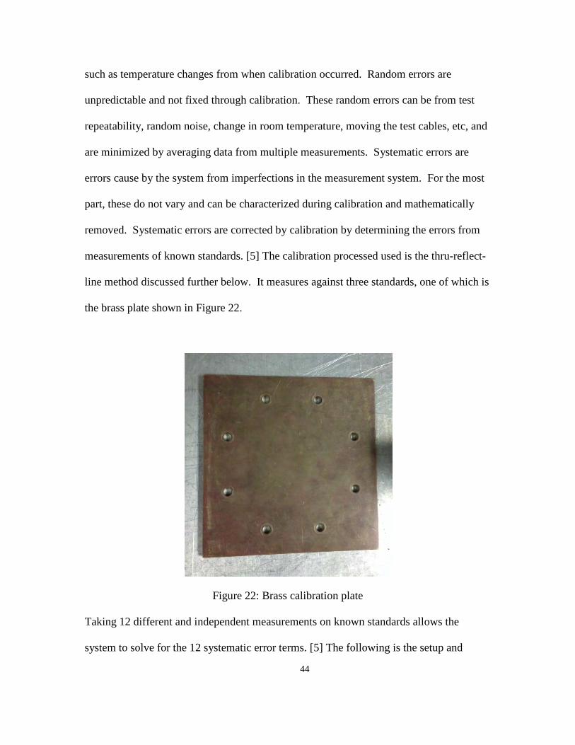
measurements of known standards. [5] The calibration processed used is the thru-reflect-
line method discussed further below. It measures against three standards, one of which is
the brass plate shown in Figure 22.
Figure 22: Brass calibration plate
Taking 12 different and independent measurements on known standards allows the
system to solve for the 12 systematic error terms. [5] The following is the setup and

45
calibration process used to prepare the network analyzer for measurements. To conduct
the S parameter measurements, the system must be set up with the appropriate coaxial
cables. The coaxial cable transmits the signal between the network analyzer and the
transmitters and receivers in the waveguide. Maury microwave 8944C38 coaxial cables
are used.
Figure 23: Coaxial cable connector
Torque wrenches are used to tighten the coaxial cables to the network analyzer. The
torque wrenches, Figure 24, tighten the connectors between .9 to 1.36 Newton-meters (8
to12 in-lbs). They prevent the cables from being over torqued and damaging the
connectors.

46
Figure 24: Torque wrenches
Using the same torque wrench, we attached the appropriate waveguide sections. To
measure in the desired frequency range, we used a WR-90 waveguide model X103A5, as
shown in Figure 25.
Figure 25: WR-90 waveguide section with coaxial connector
The next step in the calibration process is setting the network analyzer for a two-port
calibration. The power is put on the network analyzer and one waits for the system to
boot. The below steps were used to calibrate the system.

47
Setting up the network analyzer for calibration:
• Select “Channel” menu o “Start and Span”
7-13 GHz (X-band) • Select “Sweep” menu
o Select “Number of Points” Select appropriate number for resolution needed
• Select 401 as a good default o Set “IF Bandwidth” to 50 Hz o Go to “Sweep setup”
Click Stepped Sweep box (put a check in it) In Dwell time, set to appropriate time
• Select 20 ms as a good default o This allows the system to be in a “steady state”
before taking data • Select “System” menu
o Go to “Configure” Select “System "𝑍0"
• Set to appropriate resistance o For rectangular waveguides, set to 1 ohm
These steps set the range at which data is to be collected, the number of data points to be
collected, and at what frequency intervals the data is collected. The impedance, 𝑍0, is set
to 1 ohm for rectangular waveguides. The setup process requires additional steps before
the calibration is completed.
• Select “Calibration” menu o Clamp the 2 plates together and measure the thickness using the digital
calipers These plates become part of the waveguide, and the network
analyzer needs to know the additional time it will take the waves to travel this additional distance.

48
Figure 26: Metal mounting plates
o Select “Advanced modified cal kit” Scroll and find “X clamp flange”
• Click “edit kit” o Select “X band ¼ wavelength line
Click “edit” • Select “Delay characteristics”
o Change to appropriate delay based on thickness of the two plates and speed of light For plates pictured
use negative 43.86367237 micro seconds
o Select “Shorts” Make sure all are zeros or ones
o Select “Thru” Make sure all are zeros and ones
o Select OK o Select OK
These steps tell the system the type of calibration kit being used including the waveguide
type and mounting bracket. The delay characteristic input comes from the additional
length the EM wave has to travel from end to end (port a to port b) because of thickness

49
of the metal mounting plates. The thickness is multiplied by the speed of light to
determine this time delay.
Once the system is setup for the calibration, you can begin to calibrate the
network analyzer. The system is calibrated using the thru-reflect-line (TRL) two-port
calibration technique. The TRL technique solves the 12 error terms and is primarily used
in calibrating non-coaxial systems, such as waveguides. The biggest advantage of the
TRL calibration method is that the required standards are easily designed, fabricated, and
characterized. [5] To calibrate the network analyzer, the following was conducted.
Calibrating the network analyzer
• Select “Calibration” menu o Select “Cal wizard”
Click next o Click TRL
View select cal kit • Scroll and select “X clamp flange”
o Click OK • Click next
Select “TRL ref plane” • Check box “Reflect standard” • Check box “System impedance” • Click next
Note: Try not to move the coaxial cables to max extent possible, as this would add
systematic errors.
• Now measure “line standard” o This is with the wave guides together o Use guide pins to align the two waveguides
Clamp them together

50
Figure 27: Line standard measurement
o On the network analyzer, hit the green button that says “line”
Analyzer will measure until you see a check mark o Now disconnect the wave guides
• Now measure “thru” o This is with the 2 plates in the wave guide
Figure 28: Thru measurement
o On the network analyzer, hit the green button that says “thru”

51
Analyzer will measure until you see a check mark • Now measure “Short”
o This is adding a brass plate between the two other plates
Figure 29: Short measurement with the brass plate between the two mounting plates
o On the network analyzer, hit the green button that says “Short” Analyzer will measure until you see a check mark
• Calibration is now complete
The TRL calibration technique measured multiple signal transmissions in the three
different scenarios to solve the twelve error terms. First, it measures the output and input
signals through just the waveguide fixture, then through the fixtures and mounting plates,
then using a brass plate to short circuit the system. The system is now calibrated and
ready to take S parameter measurements, but it is important to watch the test setup and
procedure to ensure systematic errors are minimized. With the calibration complete, the
system is ready for the samples. Figure 30 shows the two waveguide sections separated
and the section between the two aluminum plates is where the sample under test is
placed. For reference, port 1is the cable connected to the left waveguide section, and port

52
2 is connected to the right sections as shown in Figure 30. The S parameter 𝑆21 is the
signal sent from port 1 to port 2 (or from left to right). The side of each sample that has
the coating or film will be placed facing port 1, this will become more evident in later
sections. This means we are focused on the waves traveling from port 1 to port 2, 𝑆21,
and the waves reflecting from port 1 back to port 1, 𝑆11.
Figure 30: Test section
3.3 Transmission reflection method testing
Each sample material will be tested in random locations along the entire sample.
Special caution is taken to ensure the area being tested is not within .5cm of the edges to
minimize possible edge effects. The purpose is to measure different areas of the sample
and gather multiple S parameter data sets. The multiple data sets will help ensure a
certain degree in confidence in the data but also potentially give a little insight on how
the variability in manufacturing across the sample may affect measurements.
The waveguide collects data on a 2.286 by 1.016 mm (.9" by .4") area of the
material . This allows us to collect multiple data sets for each material. For example,
Figure 31 shows the baseline sample.

53
Figure 31: Baseline composite
The sample is approximately 17 by 5 cm (7" by 2") and all samples are of similar size. In
Figure 20, the sample is on a gridded table where each square is 1 cm by 1 cm. The
thickness for each sample was collected at five different locations and varied by location.
Table 1 are the measured thicknesses.
Table 1: Measured sample thicknesses
Measure Sample Thickness (mm)
Measurement Baseline CNTs Ni-coated
CNTs Pyrolitic Graphite P100 fibers
1 0.79 0.75 1.27 1.67 1.23 2 0.81 0.66 1.21 1.76 1.34 3 0.76 0.86 1.13 1.75 1.29 4 0.79 0.72 1.25 1.77 1.25 5 0.75 0.74 1.09 1.82 1.3
Average 0.78 0.746 1.19 1.754 1.282
The thickness is used in the algorithms to process the data and determine the electrical
properties for each sample. Figure 32 shows the baseline composite in the test setup.

54
Figure 32: Baseline composite in the test section.
3.4 Testing the Materials
Once in the test section the two mounting plates are aligned together by four aligning
screws (one in each corner), and the two sections are tightly clamped together. This
allows the materials to sit flush against the opening in the two waveguide sections.
Figures 33 shows the baseline composite ready for testing, and Figure 34 shows the P100
fiber composite ready for testing.
Figure 33: Baseline composite in testing

55
Figure 34: P100 fiber in testing
Once in the test section, the network analyzer conducts a sweep between the selected
frequencies and records the data. This process is repeated 30-33 times at different
sections on each sample. The data is then saved and transferred to a flash drive for data
processing in MATLAB. For the purpose of this research it assumed there is not air gap
between the material under test and the waveguide, this of course is not entirely true.

56
3.5 Resistivity Measurements
The surface resistivity measurement is conducted using the Guardian SRM-232
2000 and four point probe, shown in Figures 35 and 36.
Figure 35: Surface resistivity meter
Figure 36: 4 point probe
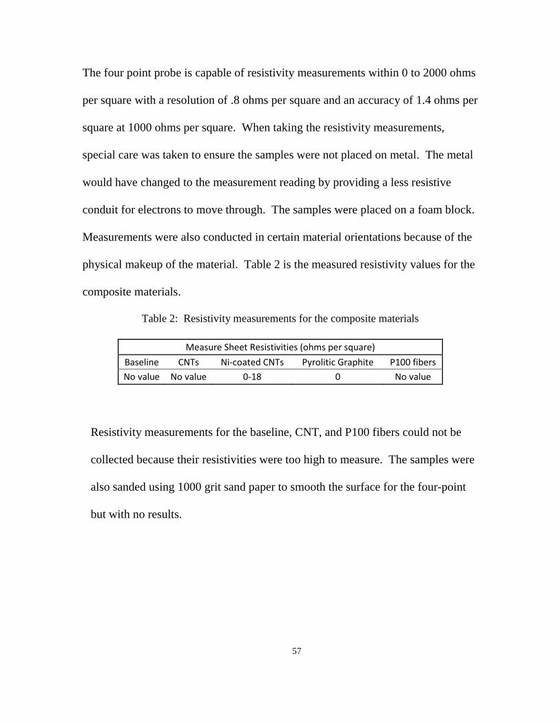
57
The four point probe is capable of resistivity measurements within 0 to 2000 ohms
per square with a resolution of .8 ohms per square and an accuracy of 1.4 ohms per
square at 1000 ohms per square. When taking the resistivity measurements,
special care was taken to ensure the samples were not placed on metal. The metal
would have changed to the measurement reading by providing a less resistive
conduit for electrons to move through. The samples were placed on a foam block.
Measurements were also conducted in certain material orientations because of the
physical makeup of the material. Table 2 is the measured resistivity values for the
composite materials.
Table 2: Resistivity measurements for the composite materials
Resistivity measurements for the baseline, CNT, and P100 fibers could not be
collected because their resistivities were too high to measure. The samples were
also sanded using 1000 grit sand paper to smooth the surface for the four-point
but with no results.
Measure Sheet Resistivities (ohms per square) Baseline CNTs Ni-coated CNTs Pyrolitic Graphite P100 fibers No value No value 0-18 0 No value

58
IV. Results and Analysis
This chapter is broken down into the several parts of the experiments to meet the
thesis objectives. Within each of these sections will be the recorded results and analysis.
For all samples, data was collected between a frequency range of 7-13 GHz, do note the
X-band range is approximately 8.2-12.4 GHZ. Also between 30-33 samples were
collected for all composite materials. This was to ensure an adequate number of samples
were taken over the entire sample to have a better representation of the data due to any
number of different variables. However, not all these data are used due to errors. This
helps reduce errors in data collection and allows us to try to calculate permittivity with a
degree of confidence. Permeability for these materials is assumed and should be
calculated to be about one with the exception of the nickel-coated CNTs. Nickel is a
ferrous materials and has a relative permeability higher than one. Individual runs of data
will not be labeled in the graphs as we are more concerned with the trend in the data, but
individual data sets will also be presented.
4.1 Permittivity from NRW algorithm
The complex permittivity for each material was calculated using the NRW
algorithm with questionable results. The results of the permittivity were found to be
inconsistent and not possible across the different materials. The following Figure 37
shows the results using the NRW algorithm to calculate the imaginary part of the
permittivity from the first five data sets of the baseline composite.

59
Figure 37: Baseline composite imaginary permittivity (runs 1-5)
The imaginary part of the permittivity should be a negative number as this relates to the
dielectric losses in the material. In addition, the permeability is calculated as a check to
ensure the data is correct. For nonferrous materials, the permeability should be
approximately that of free space; therefore in terms of relative permeability, be equal to
one. Figure 38 shows the permeability calculated by the NRW algorithm for the baseline
configuration’s first five data sets.
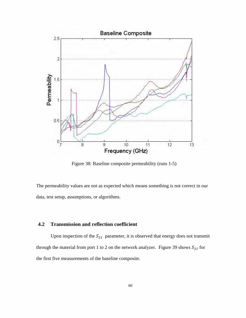
60
Figure 38: Baseline composite permeability (runs 1-5)
The permeability values are not as expected which means something is not correct in our
data, test setup, assumptions, or algorithms.
4.2 Transmission and reflection coefficient
Upon inspection of the 𝑆21 parameter, it is observed that energy does not transmit
through the material from port 1 to 2 on the network analyzer. Figure 39 shows 𝑆21 for
the first five measurements of the baseline composite.

61
Figure 39: Magnitude of 𝑆21 for the baseline composite (runs 1-5)
The magnitude of the 𝑆21 parameter represents the transmission of the electric field
through the composite, the transmission coefficient. In Figure 39, the 𝑆21 value is
approximately zero. This concludes that energy is not transmitting through the material
(at least not measureable amounts with the equipment). This becomes an issue when
trying to use the NRW algorithm. The NRW algorithm requires two equations
(𝑆11 and 𝑆21) to solve for permittivity and permeability. To verify energy is not
transmitting through the material, we will look at the magnitude of the 𝑆11 parameter,
which is the reflection coefficient.

62
Figure 40: Magnitude of 𝑆11 for the baseline composite (runs 1-5)
It is shown in the figure that the reflection coefficient is relatively near one. This
indicates most of the energy reflects off the sample. A closer examination of a data set
will show that not all the energy is reflected or transmitted. Figure 40 shows the
transmission and reflection coefficient for the same measurement or data set. At 10 GHz,
the reflection coefficient is calculated at .9481, and the transmission coefficient is .00399.
The reflection and transmission coefficients would add to 1 in a no loss scenario in which
all the energy is either transmitted or reflected. In the case of the measurements in this
thesis, it is expected energy is lost in the form of heat in the material under test. Other

63
potential losses are due to the aluminum walls in the WR-90 waveguides, but these are
assumed perfect electrical conductors and therefore have negligible losses.
Figure 41: Transmission and reflection coefficient for one measurement
4.3 Power coefficients
From the reflection coefficients, you can determine the power coefficient of
reflection. The power coefficient is the amount of power lost at reflection and can be
easily calculated as the square of the reflection coefficient, magnitude of 𝑆11. We will
use this term to determine which material is best suited to most efficiently reflect X-band
electromagnetic energy.

64
4.3 .1 Brass Plate
The brass plate was used for calibration and represents a perfect electrically
conducting material to the network analyzer. In the Figure 42, the brass plate will have a
power coefficient of one. This indicates it reflects all power back. While we know this is
not possible because of losses, we still consider it as perfect reflector of the EM energy.
The network analyzer and S parameter measurements do not have the resolution to
distinguish between the brass plate and one of copper or silver where would be silver the
superior reflector in this application.
Figure 42: Power coefficient for the brass plate

65
Figure 43 is the brass plate’s power coefficient at a zoomed in scale. Notice the power
coefficient is within a thousandth of a percent of one (within the expected noise). This
means almost all the power is reflected. Notice it is a positive 1 and does not show
direction of the reflected power.
Figure 43: Power coefficient for the brass plate (magnified)
In addition, there is very little phase shift (or dielectric losses) with the brass plate.
Figure 44 is the imaginary part of the reflection coefficient and represents the change in
phase angle of the reflected wave. It is within a 1/1000th of a percent to zero meaning
there is a -180 degree shift in the phase angle as it is reflected.

66
Figure 44: Imaginary part of the reflection coefficient

67
4.3 .2 Baseline composite
Figure 45 shows the calculated power coefficient for the baseline
composite. Each line represents 1 of the 33 measurements collected.
Figure 45: Power coefficient for the baseline composite
With the baseline composite, you see a drop in performance compared to the brass plate.
The power coefficient is between 87.43-91.9% at 10 GHz and steadily decreases as the
frequency increases. Figure 46 is the trend line calculated from Figure 44 above. The
trend line is calculated as a quadratic polynomial. At 10 GHz, the power coefficient on
the trend line is 89.2%.

68
Figure 46: Power coefficient trend line for the baseline composite
These data will be analyzed and compared to the similar data from the other materials
and allow a fair comparison among the different composites. Figure 47 shows the
calculated power coefficient for the CNT infuse composite. Each line represents 1 of 33
measurements collected for this sample.

69
4.3 .3 CNT Composite
Figure 47 shows the calculated power coefficient for the CNT infused composite.
Each line represents 1 of 33 measurements collected for this sample.
Figure 47: Power coefficient for the CNT composite
With the CNT composite, the power coefficient falls between 90.17-93.25% power
coefficient at the 10 GHz frequency and steadily decreases as the frequency increases.
Figure 48 is the trend line calculated from Figure 47 above. The trend line is calculated
as a quadratic polynomial. At 10 GHz, the power coefficient is 91.51%.

70
Figure 48: Power coefficient trend line for the CNT composite

71
4.3 .4 Nickel coated CNT Composite
Figure 49 shows the calculated power coefficient for the Nickel coated
CNT infused composite. Each line represents 1 of the 31 measurements collected.
Figure 49: Power coefficient for the Nickel coated CNT composite
With the Ni-coated CNT composite, the power coefficient falls between 65.41-83.50%
power coefficient at the 10 GHz frequency and steadily decreases as the frequency
increases. Figure 50 is the trend line calculated from Figure 49 above. The trend line is
calculated as a quadratic polynomial. At 10 GHz, the power coefficient is 91.51%.

72
Figure 50: Power coefficient trend line for the Nickel coated CNT composite

73
4.3 .5 P100 Fiber Composite
Figure 51 shows the calculated power coefficient for the P100 fiber composite.
Each line represents 1 of the 32 measurements collected.
Figure 51: Power coefficient for the P100 fiber composite
The P100 fiber’s measurements is quite different from the other composites in that the
power reflection coefficient data in Figure 51 follow a periodic/sinusoidal type pattern.
In analyzing the data, many of the data runs seem to consistently valley and peak at the
same frequencies. The reason may be the wavelengths at these frequencies and the
geometric alignment of the fibers. The spacing or physical dimension of the composite

74
surface may be some factor of the wavelengths at those frequencies. The power
coefficient falls between 88.22-93.20% power coefficient at the 10 GHz frequency and
steadily decreases as the frequency increases. Figure 52 is the trend line calculated from
Figure 50 above. The trend line is calculated as a quadratic polynomial. At 10 GHz, the
power coefficient is 90.34%.
Figure 52: Power coefficient trend line for the P100 composite

75
4.3 .6 Pyrolitic graphite
Figure 53 shows the calculated power coefficient for the pyrolitic graphite
composite. Each line represents 1 of the 5 measurements collected.
Figure 53: Power coefficient for the pyrolitic graphite fiber composite
With the pyrolitic graphite composite, the power coefficient falls between 98.32-99.82%
power coefficient at the 10 GHz frequency and generally stays level as the frequency
increases. Figure 48 is the trend line calculated from Figure 47 above. The trend line is
calculated as a quadratic polynomial. At 10 GHz, the power coefficient is 98.82%.

76
Figure 54: Power coefficient trend line for the pyrolitic graphite composite
4.4 Power coefficient comparison of the materials
For each material, the power coefficients were calculated and presented
individually. This section will conduct a comparison of each materials calculated power
coefficient trend line to determine the effects there differences have on the power
coefficient in the X-band frequency range. Figure 55 and 56 shows the trend lines for the
composite materials. Table 3 gives power coefficient values at five distinct frequencies.

77
Figure 55: Power coefficient trend lines of the composite materials
Figure 56: Power coefficient trend lines of the composite materials

78
Table 3: Frequency versus power coefficients for different materials trend lines
Specific Power Coefficient Data from Trend Lines Frequency (GHz) Baseline CNTs Ni-coated CNTs Pyrolitic Graphite P100 fibers
8.2 91.6% 94.7% 75.6% 100.8% 92.9% 9 90.4% 93.9% 71.4% 100.8% 91.4%
10 89.2% 93.0% 66.1% 100.7% 90.4% 11 88.5% 92.4% 60.7% 100.6% 89.7%
12.4 87.9% 91.7% 53.0% 100.4% 89.3% Average 89.5% 93.1% 65.3% 100.6% 90.7%
The addition of CNT, P100 fiber, and pyrolitic graphite to the baseline carbon
fiber composite improved the overall power coefficient throughout the X-band frequency
range. With the exception of the pyrolitic graphite, the composites power coefficient
decreased as the frequency increase. This is expected because as the frequency increase,
the wavelengths become smaller and smaller. This increases the ratio between the
wavelength and the material’s surface roughness. As the roughness of the composite
becomes on the order of skin depth, attenuation increases. Skin depth is the distance the
EM energy travels into the material, or how deep into the material it penetrates, before
the conductivity density is reduced to 1/e of the original value at the material’s surface.
Skin depth is a function of conductivity, frequency, and a material’s permeability. Figure
57 shows how the ratio of surface roughness and skin depth increase the attenuation
(or losses). [31]

79
Figure 57: Attenuation versus surface roughness
As the wavelength become smaller, bumps and roughness caused by the fibers weave,
resin, and other added materials become relatively larger with respect to the wavelength.
For example, the EM wave at 4 GHz with a 15cm wavelength will be less affected by the
small surface imperfections of the composites compared to the wavelength of 3cm at
10 GHz.
The addition of the Ni-coated CNTs decreased the power coefficient of the
composite across the entire frequency. This is somewhat surprising as Nickel is
considered a conductive metal used in a variety of applications. There are two potential
reasons why this may occurred. As discussed before, the Ni-coated CNTs may have
increased the surface “roughness” due to the additional size of the CNTs from the nickel
coating. The CNTs alone were approximately 60nm, but the Ni-coated CNTs received an
additional 30nm of the nickel coating. However, at this frequency range the surface
80
roughness seems unlikely to cause a drop in performance because the wavelengths at this
frequency range are larger in comparison to the material’s surface roughness.
Another reason the performance may have dropped is due to nickel’s large skin
depth. As discussed, skin depth is a function of frequency, conductivity, and
permeability.
𝛿𝑠 = � 22𝜋𝑓𝜇𝜎
(24)
Compared to copper, nickel has a much larger skin depth because nickel has larger
conductivity and a 200+ times the permeability. However, compared to graphite and
carbon, nickel has a much smaller skin depth. Another area of concern is that for a given
weight fraction, the Ni-coated CNTs are much heavier than their nickel-less counter
parts. Therefore, there are much more of the regular CNTs which create much more
interconnects throughout the epoxy resin. This allows electrons to move about more
freely.

81
V. Conclusions and Recommendations
The results were presented after conducting many experiments. Different carbon
based composites were manufactured and compared. Not all testing goals were met. The
sheet resistivity measurements could not be accomplished. This chapter will draw over all
conclusions from the data and have future recommendation for research.
5.1 Conclusions
The objective of this research was to characterize composite materials for use in
load bearing waveguides. The waveguide will be designed as a multifunctional part,
capable of supporting structural loads and propagating EM energy for use in an antenna
array. The study compared the power coefficient of five different composites. Each
composite was made of Grafil 34-700 carbon fiber and EPON 862 epoxy. The results
show that the baseline composite reflected approximately 89.5% of the RF power. Four
different carbon based materials were combined with the carbon fiber epoxy to study
their affects on the composite’s RF performance: CNTs, nickel coated CNTs, pyrolitic
graphite, and P100 fibers.
The CNTs were mixed into the resin and cured in an autoclave with the carbon
fiber weave. The study has shown that adding CNTs to a composite improves the
composites ability to reflect electromagnetic energy by an average of 3.6%.
Additionally, nickel coated CNTs were examined. The results found that the addition of
Ni-coated CNTs dramatically reduced the RF performance of the waveguide. The Ni-
82
coated CNT composite saw a reduction of about 24.2% in the amount of power reflected
back.
P100 fibers are aligned and cured onto the baseline composite. The results for the
P100 composite show a cyclic pattern in the power coefficient. The P100 composite
resulted in a 1.2% increase in performance as compared to the baseline composite, but
that value can vary more dramatically depending on where you select the data. Overall it
improves the performance over the baseline composite. The pyrolitic graphite composite
has the best performance compared to the other tested materials. The addition of the
pyrolitic graphite layer resulted in an increase in performance of around 8.4%. The
substantial increase is attributed to the atomic structure of the graphite.
The primary goal of this research was to determine the permittivity of the
composite materials to calculate the ohmic losses of the tested material in a waveguide
design. Unfortunately, the presented NRW algorithm was not able to process the data
because there is not enough information to calculate all the unknowns. Still, power
reflection coefficients are calculated and offer insight as to how well the material reflects
the RF energy.
5.1 Recommendations and Suggestions for Future Work
This research focused on the electrical performance function of the load-bearing
waveguide. A parallel study on the effects of the additional carbon based materials to the
structural performance of the waveguide would offer valuable information. The
information could be used from a systems design level to determine how to tailor the

83
composite waveguide for this application, and offer inputs to the trade space in designing
this multi-functional component. The addition of CNTs improved the electrical
performance of the waveguide, but additional research can focus on varying the types,
amounts, size, etc of the CNTs to determine if an optimal solution exists to achieve the
electrical and mechanical requirements.
Additionally, this research determined the NRW algorithm is not a viable option
to determine the permittivity of the composites. To calculate permittivity, a new
algorithm must be developed and used. One potential solution is the short circuit line
iterative conversion method. [32] This technique is an iterative process that only requires
reflection data and a good initial guess to calculate the permittivity.
In addition, an accurate resistivity measurement could not be obtained with the
equipment at AFIT. A method needs to be developed to determine the resistivity of the
composite materials. With the resistivity and permittivity methods determined, different
composites can be compared and the theoretical performance of a waveguide made of
these materials can be calculated. From this, a waveguide can be manufactured and
tested to verify the model.
Designing a load-bearing composite waveguide offers many challenges and
research opportunities across a spectrum of disciplines. There are material, electrical,
and mechanical considerations when designing a load-bearing waveguide and research in
all these fields is required to formulate an optimal solution. There are many different
areas one can explore to help engineer a solution, and it is recommended that the research
continue in some form or fashion.
84
VI. Bibliography
[1] M. Mirotznik, S.Yarlagadda, R. McCauley, and P. Pa, “Broadband Electromagnetic Modeling of Woven Fabric Composites,” IEEE Trans. Microwave Theory and Techniques, vol. 60, no. 1,pp. 158-169, Jan. 2012.
[2] K. Bal and V. K. Kothari, “Permittivity of woven fabrics: A comparison of
dielectric formulas for air-fiber mixture,” IEEE Trans Dielect. Electr. Insulation, vol. 17, no. 3, pp. 881-889, Jun. 1993
[3] S.C. Nemat-Nasser, A. Amirkhizi, T. Plaisted, J. Isaacs, and S. Nemat-Nasser,
“Structural composites with integrated electromagnetic functionality,” in Proc. SPIE, 2002, vol. 4698, pp. 237-245.
[4] D. Micheli, R.Pastore, C. Apollo, M. Machetti, G. Gradoni, V. Primiani and F.
Moglie, “Boradband Electromagnetic Absorbers Using Carbon Nanostructure-based Composites,” IEEE Trans. Microwave Theory and Techniques, vol. 59, no. 10, pp.2633-2646, Oct. 2012.
[5] Chen, Lin-Feng. Microwave Electronics: Measurement and Materials
Characterisation. Weinheim [u.a.: Wiley, 2004. Print.
[6] Balanis, Constantine A. Advanced Engineering Electromagnetics. New York: Wiley, 1989. Print.
[7] Wong, H. -S. Philip, and Deji ,. Akinwande. Carbon Nanotube and Graphene Device Physics. Cambridge [etc.: Cambridge UP, 2011. Print.
[8] Mallick, P. K. Fiber-reinforced Composites: Materials, Manufacturing, and Design. Boca Raton, FL: CRC, 2008. Print.
[9] Sabat, Joseph W. Structural Response of the Slotted Waveguide Antenna
Stiffened Structure Components under Compression. MS Thesis. Air Force Institute of Technology (AU), Wright-Patterson AFB OH, Mar 2010.
[10] Slepyan, Gregory Ya., Sergey A. Maksimenko, Oleg M. Yevtushenko, and Anton V. Gusakov. "Electronic and Electromagnetic Properties of Nanotubes." Physical Review B 57.16 (1998): 9485-497. Print.
[11] Watts, P. "The Complex Permittivity of Multi-walled Carbon Nanotube–polystyrene Composite Films in X-band." Chemical Physics Letters 378.5-6 (2003): 609-14. Print.

85
[12] Do, Van Nam, and Thanh Huy Pham. "Graphene and Its One-dimensional Patterns: From Basic Properties towards Applications." Advances in Natural Sciences: Nanoscience and Nanotechnology 1.3 (2010): 033001. Print.
[13] Slepyan, G. Ya., S. A. Maksimenko, O. Yevtushenko, and A. V. Gusakov.
"Electrodynamics of Carbon Nanotubes: Dynamic Conductivity, Impedance Boundary Conditions, and Surface Wave Propagation." Physical Review B 60.24 (1999): 17136-7149. Print.
[14] Ra Shuba, M. V., G. Ya. Slepyan, S. A. Maksimenko, C. Thomsen, and A.
Lakhtakia. "Theory of Multiwall Carbon Nanotubes as Waveguides and Antennas in the Infrared and the Visible Regimes." Physical Review B 79.15 (2009). Print.
[15] Zhu, Q., L. Wu, S. Sheng, Z. C. Mei, W. F. Liu, W. L. Cai, and L. Z. Yao. "Possibility of Constructing Microwave Antenna with Carbon Nanotubes." Journal of Vacuum Science & Technology B: Microelectronics and Nanometer Structures 25.5 (2007): 1630. Print.
[16] Micheli, D., C. Apollo, R. Pastore, and M. Marchetti. "X-Band Microwave
Characterization of Carbon-based Nanocomposite Material, Absorption Capability Comparison and RAS Design Simulation." Composites Science and Technology 70.2 (2010): 400-09. Print.
[17] Highered.mcgraw-hill.com. 5 May 2003. Magraw-HIll Publishing. 16 Feb 2012 <highered.mcgraw-hill.com/sites/dl/free/0072549076/ch07.pdf>
[18] Wagner, R., and Ingvarson, P., 1982. “Synthetic Aperture Radar from CFRP.”
In Digest International Geoscience and Remote Sensing Symposium (IGARSS), Vol. 1, Dornier Systems GmBH and Ericsson, IEEE, pp. 4.1-4.6
[19] Institute of Electrical and Electronics Engineers, “The IEEE standard dictionary of electrical and electronics terms”; 6th ed. New York, N.Y., Institute of Electrical and Electronics Engineers, c1997. IEEE Std 100-1996. ISBN 1-55937-833-6 [ed. Standards Coordinating Committee 10, Terms and Definitions; Jane Radatz, (chair)]
[20] www.merriam-webster.com. Encyclopedia Britannica. 16 Feb 2012 <http://www.merriam-webster.com/dictionary/composite>
[21] Rosker, M. Integrated Sensor Is Structure (ISIS). <http://www.darpa.mil/mto/programs/isis/>.
[22] Callus, P. J., 2006. Conformal Load-Bearing Antenna Structure for Australian Defence Force Aircraft. Version 0.1, Australian Defense Science and

86
Technology Oraganisation, Fishermans Ben, Victoria, Australia.
[23] Mitchell, S.”Electromagnetic Wave Propagation: Theory and Application to Bathymetric Lidar Simulation.” 19 Dec 2008 <http://ccar.colorado.edu/~semitche/asen6849/EM_propagation.pdf 3>.
[24] IPE Nanotube Primer. 17 Feb 2012. <http://ipn2.epfl.ch/CHBU/NTbasics1.htm>.
[25] M. Y. Han, B. Ozyiluaz, Y. Zhang and P. Kim, Energy band-gap engineering of graphene nanoribbons. Phys. Rev. Lett., 98 (2007) 206805.
[26] X. Li, X. Wang, L. Zhang, S. Lee and H. Dai, Chemically derived, ultrasmooth graphene nanoribbon semiconductors. Science, 319 (2008) 1229-32
[27] " Momentive.com - EPON Resin 862." Momentive.com - World Leader in Specialty Chemicals and Materials. N.p., n.d. Web. 27 Feb. 2012. <http://www.hexion.com/Products/TechnicalDataSheet.aspx?id=3950>.
[28] Zhu, J., Peng, H., Rodriguez-Macias, F., Margrave, J., Khabashesku, V., Imam, A., Lozano, K., Barrera, E. Reinforcing epoxy polymer composites through covalent integration of functionalized nanotubes. Advanced Functional Materials, 2004. 14(7): p. 643-648.
[29] Theodore, Martin , Mahesh Hosur, Johnathan Thomas, and Shaik Jeelani. "ICCM - Home Page." ICCM - Home Page. International Committee on Composite Materials , n.d. Web. 23 Feb. 2012. <http://www.iccm-central.org/Proceedings/ICCM16proceedings/contents/pdf/MonA/MoAA2-01sp_theodorem222779p.pdf>.
[30] Eletskii, A. "Transport propeties of carbon nanotubes." Physics-Uspekhi 52 (2009): 209-224. Print.
[31] Edwards, Terry, and a Wiley book.. "Surface Roughness - Microwave Encyclopedia - Microwaves101.com." Microwaves101.com - A practical resource covering the fundamental principles of microwave design. N.p., n.d. Web. 27 Feb. 2012. <http://www.microwaves101.com/encyclopedia
[32] "Measurement of dielectric material properties." http://www.rohde-schwarz.cz/. Version RAC0607-0019. Rhode and Schwarz, n.d. Web. 25 Feb. 2012. <www.rohde-schwarz.cz/file_3463/RAC-0607-0019.pdf>.

87
REPORT DOCUMENTATION PAGE Form Approved OMB No. 0704–0188
The public reporting burden for this collection of information is estimated to average 1 hour per response, including the time for reviewing instructions, searching existing data sources, gathering and maintaining the data needed, and completing and reviewing the collection of information. Send comments regarding this burden estimate or any other aspect of this collection of information, including suggestions for reducing this burden to Department of Defense, Washington Headquarters Services, Directorate for Information Operations and Reports (0704–0188), 1215 Jefferson Davis Highway, Suite 1204, Arlington, VA 22202–4302. Respondents should be aware that notwithstanding any other provision of law, no person shall be subject to any penalty for failing to comply with a collection of information if it does not display a currently valid OMB control number. PLEASE DO NOT RETURN YOUR FORM TO THE ABOVE ADDRESS. 1. REPORT DATE (DD–MM–YYYY) 29-02-2012
2. REPORT TYPE Master’s Thesis
3. DATES COVERED (From — To) 7 April 10 – 22 March 2012
4. TITLE AND SUBTITLE Material Characterization for Composite Materials in Load Bearing Wave Guides
5a. CONTRACT NUMBER
5b. GRANT NUMBER
5c. PROGRAM ELEMENT NUMBER
6. AUTHOR(S) Almodovar, Gabriel, Capt, USAF
5d. PROJECT NUMBER 5e. TASK NUMBER
5f. WORK UNIT NUMBER
7. PERFORMING ORGANIZATION NAME(S) AND ADDRESS(ES) Air Force Institute of Technology Graduate School of Engineering and Management (AFIT/ENY) 2950 Hobson Way WPAFB OH 45433-7765
8. PERFORMING ORGANIZATION REPORT NUMBER AFIT/GAE/ENY/12-M01
9. SPONSORING / MONITORING AGENCY NAME(S) AND ADDRESS(ES) Mr William Baron (937) 798-4946 [email protected] AFRL/RB 2130 8TH ST B20045 R121 WPAFB, OH 45433
10. SPONSOR/MONITOR’S ACRONYM(S) AFRL/RB
11. SPONSOR/MONITOR’S REPORT NUMBER(S)
12. DISTRIBUTION / AVAILABILITY STATEMENT APPROVED FOR PUBLIC RELEASE; DISTRIBUTION UNLIMITED
13. SUPPLEMENTARY NOTES This material is declared a work of the U.S. Government and is not subject to copyright protection in the United States.
14. ABSTRACT This study will establish a methodology to examine samples of composite material for application in a load bearing waveguide. The composite material will operate in a specific frequency range for applications in small RPAs. A graphite epoxy stiffening component will be primarily considered. Different nickel, graphene, and carbon nanotube (CNT) coatings and films will be applied to the graphite epoxy. Tests will determine the material's radio frequency (RF) performance for application as an antenna/waveguide component. The study will use scattering (S) parameters determined from a network analyzer to collect these data. The S parameters will then be used to resolve the composites permittivity and reflectivity and allow an estimation of a full scale waveguides performance made from pretested composite material.
15. SUBJECT TERMS Waveguide, Composite, X-band, Carbon nanotubes, grapheme, permittivity
16. SECURITY CLASSIFICATION OF: 17. LIMITATION OF ABSTRACT UU
18. NUMBER OF PAGES 100
19a. NAME OF RESPONSIBLE PERSON Dr. Anthony Palazotto, AFIT/ENY
a. REPORT U
b. ABSTRACT U
c. THIS PAGE U
19b. TELEPHONE NUMBER (Include Area Code) (937) 785-3636 x4599