masters thesis: modeling and analysis of high frequency
TRANSCRIPT

Electrical Sustainable Energy
Modeling and analysis of highfrequency high voltage multipliercircuit for high voltage powersupply
Weijun Qian
Proj
ectR
epor
t

Abstract
High frequency high voltage power supply has been widely applied in many industrial appli-cations such as the medical X-ray machine and eletrostatic precipitators. As a part of thehigh frequency high voltage power supply, the electrical performances of the voltage multipliercircuit will influence the behaviors of applications like the X-ray machine such as the imagingquality. The electrical performances include the output voltage drop and voltage ripple, risetime and decay time of output voltage and power losses. In order to get high imaging qualityof the X-ray machine and reduce damage to patients, the multiplier circuit is required to bedesigned with low output voltage drop and voltage ripple as well as fast respond time.
This thesis concentrates on the investigation of the electrical performances of the Half-wave se-ries Cockcroft-Walton(HWCW) voltage multiplier circuit. The operations in start-up processand steady state are explained in details and methods to evaluate the electrical performancesare introduced. Significant parameters of the multiplier circuit that play a role in determiningthe electrical performances are investigated. Analysis of impact of the parasitic componentson the electrical performances are carried out together with simulations. An analytical powerloss model is developed in the thesis by deriviations of currents in the HWCW voltage mul-tiplier circuit. At last, optimization of capacitance distributions are discussed and comparedto provide methods when selecting the capacitance values in the circuit. The analyses in thethesis are verified by the simulation results in LTspice.
Thesis committee members:Prof.dr.ir.Pavol BauerDr.ir.Zian QinDr.ir.Jose Rueda Torres
Master thesis Weijun Qian

ii
Master thesis Weijun Qian

Acknowledgement
First of all, I would like to express my deepest gratitude to my supervisor Saijun Mao whohelps and encourages me a lot during the process of my master thesis project. Besides thecountless academic guidance, Saijun teaches me a lot about the professional attitudes as anengineer which would definitely let me benefit a lot after I have worked in the future.
I would also like to express sincere thanks to Dr.Zian Qin and Dr.Jelena Popovic-Gerber, whoteach me a lot about power electronics. This thesis wouldn’t have been done without theirhelp.
Thanks to my fellow students in ESE. We have had lots of colorful and unforgettable experi-ences together during the last two years in the Netherlands. I will never forget the memoriesabout how we studied together and how we were crazy.
Thanks to my roommates Qiuman and Jiaxing. It is happy and relaxed to live with you. Youtwo are the best roommates in the world, we have already been just like a ’family’.
At last, I would like to thank my parents. Thanks for your support and care behind weforever. Without your support, It’s impossible for me to go so far.
Master thesis Weijun Qian

iv Acknowledgement
Master thesis Weijun Qian

Table of Contents
Acknowledgement iii
1 Introduction 11-1 Problem Statement . . . . . . . . . . . . . . . . . . . . . . . . . . . . . . . . . 1
1-1-1 Medical X-ray/CT machine . . . . . . . . . . . . . . . . . . . . . . . . . 21-1-2 Voltage multiplier circuit . . . . . . . . . . . . . . . . . . . . . . . . . . 3
1-2 Thesis objectives . . . . . . . . . . . . . . . . . . . . . . . . . . . . . . . . . . . 31-3 Thesis approach and layout . . . . . . . . . . . . . . . . . . . . . . . . . . . . . 4
2 Operation Analysis of Voltage Multiplier Circuit 52-1 Start-up process analysis . . . . . . . . . . . . . . . . . . . . . . . . . . . . . . 5
2-1-1 Operations in start-up process . . . . . . . . . . . . . . . . . . . . . . . 62-1-2 Conditions for the conduction of diodes . . . . . . . . . . . . . . . . . . 82-1-3 Simulations and Discussions . . . . . . . . . . . . . . . . . . . . . . . . 9
2-2 Steady state analysis . . . . . . . . . . . . . . . . . . . . . . . . . . . . . . . . 112-2-1 Operations in steady state . . . . . . . . . . . . . . . . . . . . . . . . . 112-2-2 Simulations and discussions . . . . . . . . . . . . . . . . . . . . . . . . . 13
2-3 Voltage drop and voltage ripple . . . . . . . . . . . . . . . . . . . . . . . . . . . 152-3-1 Derivations of voltage drop and voltage ripple . . . . . . . . . . . . . . . 152-3-2 Simulations and Discussions . . . . . . . . . . . . . . . . . . . . . . . . 17
2-4 Comparative analysis of bridge diode rectifier and voltage doubler . . . . . . . . 182-4-1 Full-wave bridge diode rectifier . . . . . . . . . . . . . . . . . . . . . . . 182-4-2 Voltage doubler . . . . . . . . . . . . . . . . . . . . . . . . . . . . . . . 202-4-3 Discussions . . . . . . . . . . . . . . . . . . . . . . . . . . . . . . . . . 21
2-5 Rise time and Decay time . . . . . . . . . . . . . . . . . . . . . . . . . . . . . . 222-5-1 Analysis of rise time . . . . . . . . . . . . . . . . . . . . . . . . . . . . . 222-5-2 Analysis of decay time . . . . . . . . . . . . . . . . . . . . . . . . . . . 24
Master thesis Weijun Qian

vi Table of Contents
2-5-3 Simulations and discussions . . . . . . . . . . . . . . . . . . . . . . . . . 252-6 Other voltage multiplier topologies . . . . . . . . . . . . . . . . . . . . . . . . . 26
2-6-1 Full-wave Cockcroft-Walton voltage multiplier circuit . . . . . . . . . . . 262-6-2 Half-wave parallel voltage multiplier circuit . . . . . . . . . . . . . . . . 302-6-3 Discussions . . . . . . . . . . . . . . . . . . . . . . . . . . . . . . . . . 33
2-7 Summary . . . . . . . . . . . . . . . . . . . . . . . . . . . . . . . . . . . . . . . 35
3 Impact of Circuit Parameters on Electrical Performances 373-1 Influence of frequency to electrical performance . . . . . . . . . . . . . . . . . . 37
3-1-1 Influence of frequency to voltage drop and voltage ripple . . . . . . . . . 373-1-2 Influence of frequency to rise time . . . . . . . . . . . . . . . . . . . . . 393-1-3 Influence of frequency to decay time . . . . . . . . . . . . . . . . . . . . 40
3-2 Influence of capacitance value to the electrical performance . . . . . . . . . . . . 413-2-1 Influence of capacitance value to voltage drop and voltage ripple . . . . . 413-2-2 Influence of capacitance value to rise time . . . . . . . . . . . . . . . . . 423-2-3 Influence of capacitance value to decay time . . . . . . . . . . . . . . . . 43
3-3 Influence of output power to the electrical performance . . . . . . . . . . . . . . 443-3-1 Influence of output power to voltage drop and voltage ripple . . . . . . . 443-3-2 Influence of output power to rise time . . . . . . . . . . . . . . . . . . . 453-3-3 Influence of output power to decay time . . . . . . . . . . . . . . . . . . 46
3-4 Optimal stage number . . . . . . . . . . . . . . . . . . . . . . . . . . . . . . . . 473-5 Summary . . . . . . . . . . . . . . . . . . . . . . . . . . . . . . . . . . . . . . . 48
4 Impact of parasitic components in the circuit 494-1 Junction capacitance of diodes . . . . . . . . . . . . . . . . . . . . . . . . . . . 494-2 Parasitic components of capacitors . . . . . . . . . . . . . . . . . . . . . . . . . 53
4-2-1 Equivalent Series Resistance . . . . . . . . . . . . . . . . . . . . . . . . 544-2-2 Equivalent Series Inductance . . . . . . . . . . . . . . . . . . . . . . . . 554-2-3 Equivalent parallel capacitance . . . . . . . . . . . . . . . . . . . . . . . 58
4-3 Parasitic components of transformer . . . . . . . . . . . . . . . . . . . . . . . . 594-3-1 Influence of parasitic components to the transformer . . . . . . . . . . . 594-3-2 Influence to the electrical performance of multiplier circuit . . . . . . . . 61
4-4 Summary . . . . . . . . . . . . . . . . . . . . . . . . . . . . . . . . . . . . . . . 63
5 Power Loss Analysis of the Multiplier Circuit 655-1 Detailed switching process of diodes in HWCW voltage multiplier . . . . . . . . 655-2 Derivations of diode currents . . . . . . . . . . . . . . . . . . . . . . . . . . . . 675-3 Conduction losses of diodes . . . . . . . . . . . . . . . . . . . . . . . . . . . . . 735-4 Power losses of capacitors . . . . . . . . . . . . . . . . . . . . . . . . . . . . . . 745-5 Summary . . . . . . . . . . . . . . . . . . . . . . . . . . . . . . . . . . . . . . . 76
Master thesis Weijun Qian

Table of Contents vii
6 Optimization of Capacitance Network 776-1 Introduction . . . . . . . . . . . . . . . . . . . . . . . . . . . . . . . . . . . . . 776-2 Influence of capacitance optimization to voltage drop and voltage ripple . . . . . 786-3 Influence of capacitance distribution to respond time . . . . . . . . . . . . . . . 81
6-3-1 Rise time with capacitance optimization . . . . . . . . . . . . . . . . . . 816-3-2 Decay time with capacitance optimization . . . . . . . . . . . . . . . . . 83
6-4 Influence of capacitance distribution to power loss . . . . . . . . . . . . . . . . . 866-4-1 Diode losses with capacitance optimization . . . . . . . . . . . . . . . . 866-4-2 Capacitor losses with capacitance optimization . . . . . . . . . . . . . . 89
6-5 Summary . . . . . . . . . . . . . . . . . . . . . . . . . . . . . . . . . . . . . . . 90
7 Conclusion 937-1 Recommedation for choice of parameters . . . . . . . . . . . . . . . . . . . . . . 94
Master thesis Weijun Qian

viii Table of Contents
Master thesis Weijun Qian

List of Figures
1-1 High frequency high voltage power supply circuit . . . . . . . . . . . . . . . . . 11-2 Comparison of X-ray imaging quality . . . . . . . . . . . . . . . . . . . . . . . . 21-3 Series half-wave Cockcroft-Walton voltage multiplier circuit . . . . . . . . . . . . 3
2-1 2-stage series HWCW voltage multiplier . . . . . . . . . . . . . . . . . . . . . . 62-2 Capacitor voltage waveform in start-up process . . . . . . . . . . . . . . . . . . 62-3 Equivalent circuits in start-up process . . . . . . . . . . . . . . . . . . . . . . . 72-4 Simulation circuit of voltage quadrupler in LTspice . . . . . . . . . . . . . . . . 102-5 Results of simulation in start-up process . . . . . . . . . . . . . . . . . . . . . . 102-6 Diode current and Capacitor voltage waveform in steady state . . . . . . . . . . 112-7 Equivalent circuits in steady state . . . . . . . . . . . . . . . . . . . . . . . . . 122-8 Simulation waveform of voltage capacitor in steady state . . . . . . . . . . . . . 142-9 Simulation waveform of diode current in steady state . . . . . . . . . . . . . . . 152-10 Simulation of 6-stage HWCW voltage multiplier circuit . . . . . . . . . . . . . . 172-11 Full-wave bridge diode rectifier . . . . . . . . . . . . . . . . . . . . . . . . . . . 182-12 Waveform of output voltage of Full-wave bridge diode rectifier . . . . . . . . . . 192-13 Equivalent circuits of full-wave bridge diode rectifier . . . . . . . . . . . . . . . . 192-14 Simulation waveform of full-wave diode bridge rectifier . . . . . . . . . . . . . . 202-15 Voltage doubler . . . . . . . . . . . . . . . . . . . . . . . . . . . . . . . . . . . 202-16 Waveform of voltage doubler . . . . . . . . . . . . . . . . . . . . . . . . . . . . 212-17 Definition of rise time and decay time . . . . . . . . . . . . . . . . . . . . . . . 222-18 Simulation waveform of rise time and decay time . . . . . . . . . . . . . . . . . 252-19 2-stage Full-wave Cockcroft-Walton voltage multiplier . . . . . . . . . . . . . . . 272-20 Waveform in steady state for FWCW multiplier circuit . . . . . . . . . . . . . . 272-21 Equivalent circuits in steady state for FWCW circuit . . . . . . . . . . . . . . . 28
Master thesis Weijun Qian

x List of Figures
2-22 Simulation circuit for FWCW multiplier circuit . . . . . . . . . . . . . . . . . . . 292-23 Simulation waveform of FWCW multiplier circuit . . . . . . . . . . . . . . . . . 292-24 2-stage half-wave parallel voltage multiplier . . . . . . . . . . . . . . . . . . . . 302-25 Waveform in start-up process of parallel voltage multiplier . . . . . . . . . . . . 302-26 Equivalent circuits in start-up process of parallel voltage multiplier . . . . . . . . 312-27 Waveform in steady state of parallel voltage multiplier . . . . . . . . . . . . . . 322-28 Simulation circuit for HW parallel multiplier circuit . . . . . . . . . . . . . . . . 332-29 Simulation waveform of HW parallel multiplier circuit . . . . . . . . . . . . . . . 34
3-1 Simulation waveform of voltage regulation with different frequency values . . . . 383-2 Simulation waveform of rise time with different frequency values . . . . . . . . . 393-3 Simulation waveform of rise time with different frequency values . . . . . . . . . 403-4 Simulation waveform of voltage regulation with different capacitance values . . . 413-5 Simulation waveform of rise time with different capacitance values . . . . . . . . 423-6 Simulation waveform of rise time with different capacitance values . . . . . . . . 433-7 Simulation waveform of voltage regulation with different output power . . . . . . 453-8 Simulation waveform of rise time with different output power . . . . . . . . . . . 463-9 Simulation waveform of rise time with different output power . . . . . . . . . . . 47
4-1 Parasitic components in voltage multiplier circuit . . . . . . . . . . . . . . . . . 494-2 Waveform of voltage across junction capacitance . . . . . . . . . . . . . . . . . 504-3 Equivalent circuits in steady state with junction capacitance . . . . . . . . . . . 514-4 Waveform of capacitor voltage with junction capacitance . . . . . . . . . . . . . 524-5 Simulation waveform with junction capacitance . . . . . . . . . . . . . . . . . . 524-6 Parasitic components of capacitor . . . . . . . . . . . . . . . . . . . . . . . . . 534-7 Simulation waveform with ESR . . . . . . . . . . . . . . . . . . . . . . . . . . . 544-8 ESR jump . . . . . . . . . . . . . . . . . . . . . . . . . . . . . . . . . . . . . . 554-9 Simulation waveform with ESL . . . . . . . . . . . . . . . . . . . . . . . . . . . 564-10 LC oscillation due to ESL . . . . . . . . . . . . . . . . . . . . . . . . . . . . . . 574-11 Voltage spikes due to ESL . . . . . . . . . . . . . . . . . . . . . . . . . . . . . . 574-12 Simulation waveform of output voltage with Cpp . . . . . . . . . . . . . . . . . . 584-13 Parasitic components of transformer . . . . . . . . . . . . . . . . . . . . . . . . 594-14 Waveform at primary side of the transformer . . . . . . . . . . . . . . . . . . . . 604-15 Comparsion of waveform for Us . . . . . . . . . . . . . . . . . . . . . . . . . . . 614-16 Simulation waveform of output voltage with actual transformer . . . . . . . . . . 624-17 Simulation waveform of decay process with actual transformer . . . . . . . . . . 62
5-1 Reverse recovery of diodes in steady state . . . . . . . . . . . . . . . . . . . . . 665-2 Equivalent circuits of reverse recovery procedures . . . . . . . . . . . . . . . . . 675-3 Simulation results of actual diode models . . . . . . . . . . . . . . . . . . . . . 67
Master thesis Weijun Qian

List of Figures xi
5-4 RMS calculation model . . . . . . . . . . . . . . . . . . . . . . . . . . . . . . . 715-5 Power losses of diodes and capacitors with different frequencies . . . . . . . . . . 75
6-1 3-stage HWCW voltage multiplier circuit . . . . . . . . . . . . . . . . . . . . . . 786-2 Voltage conversion ratio with stage number in 5 methods . . . . . . . . . . . . . 806-3 Simulation waveform of voltage regulation in 5 methods . . . . . . . . . . . . . 816-4 Simulation waveform of rise time in 5 methods . . . . . . . . . . . . . . . . . . 836-5 Simulation waveform of decay time in 5 methods . . . . . . . . . . . . . . . . . 866-6 Distributions of conduction loss and capacitor loss in 5 methods . . . . . . . . . 92
Master thesis Weijun Qian

xii List of Figures
Master thesis Weijun Qian

List of Tables
2-1 Simulation parameters for voltage quadrupler circuit . . . . . . . . . . . . . . . . 92-2 Parameters of 6-stage HWCW voltage multiplier circuit . . . . . . . . . . . . . . 172-3 Comparison of calculation and simulation results of voltage drop and voltage ripple 182-4 Comparison of AC-DC voltage conversion circuits . . . . . . . . . . . . . . . . . 212-5 Rise time calculation for voltage quadrupler . . . . . . . . . . . . . . . . . . . . 232-6 Calcultion results of decay time . . . . . . . . . . . . . . . . . . . . . . . . . . . 252-7 Simulation results of rise time and decay time . . . . . . . . . . . . . . . . . . . 262-8 Voltage drop and Voltage ripple comparison . . . . . . . . . . . . . . . . . . . . 262-9 Comparison of voltage drop and voltage ripple of different topologies . . . . . . . 332-10 Advantages and Drawbacks of different rectifier circuits . . . . . . . . . . . . . . 36
3-1 Calculation results of voltage regulation with different frequency values . . . . . 383-2 Simulation results of voltage regulation with different frequency values . . . . . . 383-3 Calculation results of rise time with different frequency values . . . . . . . . . . 393-4 Simulation results of rise time with different frequency values . . . . . . . . . . . 393-5 Calculation results of decay time with different frequency values . . . . . . . . . 403-6 Simulation results of rise time with different frequency values . . . . . . . . . . . 403-7 Calculation results of voltage regulation with different capacitance values . . . . 413-8 Simulation results of voltage regulation with different capacitance values . . . . . 423-9 Calculation results of rise time with different capacitance values . . . . . . . . . 423-10 Simulation results of rise time with different capacitance values . . . . . . . . . . 433-11 Calculation results of decay time with different capacitance values . . . . . . . . 433-12 Simulation results of rise time with different capacitance values . . . . . . . . . . 443-13 Calculation results of voltage regulation with different output power . . . . . . . 443-14 Simulation results of voltage regulation with different output power . . . . . . . 45
Master thesis Weijun Qian

xiv List of Tables
3-15 Calculation results of rise time with different output power . . . . . . . . . . . . 453-16 Simulation results of rise time with different output power . . . . . . . . . . . . 463-17 Calculation results of decay time with different output power . . . . . . . . . . . 463-18 Simulation results of rise time with different output power . . . . . . . . . . . . 47
4-1 Voltage drop and voltage ripple with junction capacitance . . . . . . . . . . . . . 534-2 Parasitic components for each individual capacitor . . . . . . . . . . . . . . . . . 534-3 Equivalent values of parasitic components of capacitors per stage . . . . . . . . . 544-4 Simulation results with ESL . . . . . . . . . . . . . . . . . . . . . . . . . . . . . 564-5 Calculation results of voltage regulation with Cpp . . . . . . . . . . . . . . . . . 584-6 Simulation results of voltage regulation with Cpp . . . . . . . . . . . . . . . . . . 594-7 Simulation results of voltage regulation with actual transformer . . . . . . . . . . 614-8 Simulation results for respond time with actual transformer . . . . . . . . . . . . 63
5-1 Calculation results of tD and ID . . . . . . . . . . . . . . . . . . . . . . . . . . 715-2 Calculation results of avetage and rms values of diode currents . . . . . . . . . . 715-3 Comparison of simulation and calculation results of diode currents . . . . . . . . 725-4 Comparison of simulation and calculation results of diode currents after optimization 725-5 Diode currents under different frequencies . . . . . . . . . . . . . . . . . . . . . 735-6 Calculation results of conduction losses . . . . . . . . . . . . . . . . . . . . . . . 735-7 Simulation results of diode currents under different frequencies . . . . . . . . . . 745-8 Simulation results of conduction losses under different frequencies . . . . . . . . 745-9 Comparison of simulation and calculation results of conduction losses . . . . . . 745-10 ESR values under different frequencies . . . . . . . . . . . . . . . . . . . . . . . 755-11 Calculation results of capacitor currents and losses with different frequencies . . . 755-12 Simulation results of capacitor currents and losses with different frequencies . . . 76
6-1 Optimization methods for unequal capacitance distribution . . . . . . . . . . . . 776-2 Capacitance distribution values in five optimization methods . . . . . . . . . . . 786-3 Voltage drop and voltage ripple for five optimization methods . . . . . . . . . . 796-4 Calculation results of voltage regulation in 5 methods . . . . . . . . . . . . . . . 806-5 Simulation results of voltage regulation in 5 methods . . . . . . . . . . . . . . . 816-6 Rise time calculation for 3-stage HWCW multiplier . . . . . . . . . . . . . . . . 826-7 Simulation results of rise time in 5 methods . . . . . . . . . . . . . . . . . . . . 836-8 Calculation results of decay time in 5 methods . . . . . . . . . . . . . . . . . . . 856-9 Simulation results of decay time in 5 methods . . . . . . . . . . . . . . . . . . . 856-10 Steady state diode current values in 5 methods . . . . . . . . . . . . . . . . . . 896-11 Calculation results of conduction loss in 5 methods . . . . . . . . . . . . . . . . 896-12 Simulation results of diode currents in 5 methods . . . . . . . . . . . . . . . . . 906-13 Simulation results of conduction losses in 5 methods . . . . . . . . . . . . . . . 906-14 Calculation results of capacitor currents in 5 methods . . . . . . . . . . . . . . . 91
Master thesis Weijun Qian

List of Tables xv
6-15 Relationsip of capacitance and ESR values . . . . . . . . . . . . . . . . . . . . . 916-16 Calculation results of capacitor losses in 5 methods . . . . . . . . . . . . . . . . 926-17 Simulation results of capacitor currents in 5 methods . . . . . . . . . . . . . . . 926-18 Simulation results of capacitor losses in 5 methods . . . . . . . . . . . . . . . . 926-19 Total power losses in 5 methods . . . . . . . . . . . . . . . . . . . . . . . . . . 92
Master thesis Weijun Qian

xvi List of Tables
Master thesis Weijun Qian

Chapter 1
Introduction
1-1 Problem Statement
High voltage power supplies have been widely used in many industrial applications such aslaser, spectral analysis, medical x-ray imaging, electrostatic precipitators and so on[1][2].Moreover, high voltage power supply operated under high frequency has the advantage ofreducing its volume and cost as well as leading to higher power density design[3]. Therefore,the demands for high frequency high voltage power supplies have been increased.
The traditional use of a high voltage turns ratio step-up transformer in high frequency highvoltage power supply is limited by its parasitic components such as leakage inductance andwinding capacitance. The low efficiency and large output voltage drop and voltage ripplewill lead to bad behaviors of industrial applications like the medical X-ray machine as isintroduced in section 1-1-1. In order to produce large output voltage with small ripple, acommon high frequency high voltage power supply is composed of an ac input source, DC-Bus, a high frequency inverter, a high voltage transformer and a high voltage multiplier circuitas is shown in Figure 1-1.
VDC
Lk
Vp Vs
Vo
Voltage Multiplier
High Frequency Inverter
High Voltage
Transformer
Figure 1-1: High frequency high voltage power supply circuit
Master thesis Weijun Qian

2 Introduction
The voltage multiplier circuit is applied at the output of the high voltage transformer. Theoutput of the voltage multiplier circuit is the output of the high voltage power supply as well.The multiplier circuit plays an important role in converting the AC input to DC output andstepping up the output voltage value with small voltage ripple. Therefore, the behavior ofthe voltage multiplier circuit determines the behavior of the high voltage power supply. Thevoltage multiplier circuit are further introduced in section 1-1-2.
1-1-1 Medical X-ray/CT machine
An impontant industrial utilization for high frequency high voltage power supply is the medi-cal X-ray machine[1]. For a high-quality modern medical X-ray machine, the clarity of X-rayimaging is required to be high and the damage to patients must be kept as small as possible.The behaviors of medical X-ray machines are dependent on the electrical performances of thehigh voltage power supply including the voltage regulation(voltage drop and voltage ripple)and respond time(rise time and decay time) of output voltage[4]. Bad voltage regulation andslow respond time will result in poor X-ray imaging quality as is shown in Figure 1-2 andmore damage to patients[5].
Figure 1-2: Comparison of X-ray imaging quality
First, the input voltage value of the X-ray machine is important in order to reduce the damageto patients as well as to improve the imaging quality[6]. When the voltage value is raised, thepenetration of X-rays is enhanced and clear image can be obtained with few X-rays. Whenthe voltage value is decreased, the penetration of X-rays is decreased and more X-rays arerequired to obtain clear image. The number of X-rays absorbed by patients will also increaseand result in more damage to patients.Second, the voltage ripple of output voltage is related with the clarity of X-ray imagingbecause the difference among energy spectrum distribution of X-ray will be large if the outputvoltage ripple is large[6]. If the voltage fluctuates seriously in steady state, the penetrationabilities of phontons will also fluctuate and result in bad quality of X-ray imaging. Therefore,the voltage value is required to be DC with large value and small ripple.Moreover, the power supply is used as a pulse power supply and the respond time in one highvoltage pulsation cycle is required to be kept within tens of microseconds. When the voltage
Master thesis Weijun Qian

1-2 Thesis objectives 3
value is far smaller than its steady state value during the rising process and decay process,soft X-rays which are not effective for imaging are produced[7] and the noise will be producedas well.
At last,the power loss in the power supply circuit is another important criteria in order toreduce heating and prolong the service life of the circuit.
1-1-2 Voltage multiplier circuit
The voltage multiplier circuit is an AC-to-DC voltage conversion circuit consisting of n stages.The voltage multiplier circuit is able to produce any output voltage in principle by increasingthe number of stages[8] The effective use of voltage multiplier circuits can realize the highvoltage conversion up to 100’s kV range and are cost efficient[9]. There are several differenttopologies for voltage multiplier circuits and the most commonly used one is the series half-wave Cockcroft-Walton (HWCW) voltage multiplier circuit shown in Figure 1-3 which isapplied in this project[10]. Each stage of the HWCW voltage multiplier circuit comprises 2legs and each leg is the series connection of one diode and one capacitor.
C1 C3
C2 C4
D2 D3 D4Vin D1
...
...
C2n-1
C2n
D2n-1 D2n
vO
Stage 1 Stage 2 Stage n
Figure 1-3: Series half-wave Cockcroft-Walton voltage multiplier circuit
When the voltage multiplier circuit is loaded, there are several important electrical perfor-mance of the voltage multiplier circuit: the voltage drop&voltage ripple, the rise time&decaytime and power losses. The electrical performance will influence the behavior of industrialapplications as is introduced in section 1-1-1. Most of the completed research on the voltagemultiplier circuits are focusing on the choice of capacitance distribution value[11][12] and theimprovement of circuit topology for better output voltage regulation[13][4]. Research on thedetailed analysis of electrical performance of the voltage multiplier circuit and power losscalculation are not in-depth. Therefore, this project is focusing on the analysis and modelingof electrical performance of the HWCW voltage multiplier circuit in order to obtain betterperformance.
1-2 Thesis objectives
This master thesis project is carried out to improve the behavior of the medical X-ray machineby optimizing the high frequency high voltage power supply with the voltage multiplier circuit.
Master thesis Weijun Qian

4 Introduction
The main objective of this master thesis project is to investigate the electrical performance(voltagedrop&voltage ripple and rise time&decay time) and to prolong the serive life of the voltagemultiplier circuit.
In order to achieve the objective, there are several research questions that have to be answered:
• What are the factors that will influence the voltage drop&voltage ripple and the risetime&decay time of the HWCW voltage multiplier circuit?
• Where are the power losses in the voltage multiplier circuit coming from and how toestimate them?
• What are the criterion when selecting the operating frequency and capacitance value ofthe multiplier circuit?
1-3 Thesis approach and layout
The project is carried on based on the case study of a 2-stage series HWCW voltage multipliercircuit. All the theoretical analysis are verified with simulations in LTspice. In order to explainthe research questions above, the thesis is organized as follows:
• In chapter 2, operations in start-up process and steady state are explained in details.The causes of voltage drop and voltage ripple are explained by derivation of formulas.The introduction and analysis of rise time and decay time are illustrated as well. Atlast, different topologies are compared to explain why the HWCW multiplier circuit ischosen in this project.
• In chapter 3, the impact of different parameters on the electrical performance of themultiplier circuit are studied respectively. Simulations are made to verify the analysis.Optimal stage number are also given by calculations.
• In chapter 4, the impact of parasitics of the electrical components on the electricalperformance of the multiplier circuit are studied. The parasitic components includethe junction capacitance of diodes, ESR,ESL and parallel capacitance of capacitors,leakage inductance and winding capacitance of the transformer. Simulations are madein LTspice to verify the analysis.
• In chapter 5, the reverse recovery analysis for rectifier are analyzed and the equationsfor the diode current are derived. Power loss model is built up to evaluate the lossdistribution of the converter.
• In chapter 6, capacitance distribution is optimized. 5 optimization methods and theirinfluence to the electrical performance of the multiplier circuit are discussed respectively.
• In chapter 7, important conclusions of the analysis from chapter 2 to 6 are summarized.At last, recommendations for setting the parameters of the HWCW voltage multipliercircuit are given.
Master thesis Weijun Qian

Chapter 2
Operation Analysis of VoltageMultiplier Circuit
The commonly used series HWCW voltage multiplier circuit is composed of n stages. Ineach stage, there are two pairs of diodes and capacitors. In the start-up process, the voltageacross the capacitors are boosted step by step until steady state is reached. In steady state,voltage drop and voltage ripple will occur when the circuit is loaded. There are some im-portant electrical performances when evaluating the voltage multiplier circuit such as voltagedrop&voltage ripple and rise time&decay time. The electrical performances determine thebehavior of the high voltage power supply.
In section 2.1, how the HWCW voltage multiplier circuit works in start-up process and booststhe voltage value are explained. In section 2.2, operations of the HWCW voltage multiplierin steady state are analyzed. Section 2.3 introduces the output voltage drop and voltageripple. Different rectifier circuits are compared in section 2.4. In section 2.5, the rise timeand decay time of the multiplier circuit are introduced and analyzed. At last, comparisonbetween different voltage multiplier topologies are made in section 2.6 to explain why theHWCW voltage multiplier circuit is chosen.
2-1 Start-up process analysis
The operations in the 2-stage voltage multiplier circuit (voltage quadrupler) shown in Figure 2-1 are analyzed as a case study in this thesis.
The voltage quadrupler circuit is made up of two stages and each stage includes two legswhich is composed of the series connection of one capacitor and one rectifier. The outputload is the resistive load RLoad representing the X-ray machine. In the voltage multipliercircuit shown in Figure 2-1, C2 and C4 are the output capacitors that charge RLoad. Theoutput voltage of the voltage multiplier circuit is the voltage across RLoad which equals tothe summation of voltage across all the output capacitors.
Master thesis Weijun Qian

6 Operation Analysis of Voltage Multiplier Circuit
C1 C3
C2 C4
RLoad
D1 D2 D3 D4
vO
Vin
+
vC1
+vC3
+
vC2
+vC4
+
Figure 2-1: 2-stage series HWCW voltage multiplier
2-1-1 Operations in start-up process
In the start-up process, the voltage across capacitors are boosted from 0 to the steady statevalue step by step. Charges can be regarded as transferring from the voltage source to C1and from capacitors in low stages to capacitors in high stages. For a typical series HWCWvoltage multiplier circuit with stage number n, in the kth switching cycle of the voltage source,D2k and D2k+1 starts to conduct in the circuit (k<n). From the nth switching cycle, all thediodes will conduct once in one switching cycle. The sequence of the conducting diodes is:D2n−1,D2n−3,· · · ,D3,D1,D2n,D2(n−1),· · · ,D4,D2. The operations of voltage quadrupler circuitin start-up process are explained in this section . The waveform of voltage across capacitorsin the start-up process is shown in Figure 2-2:
Us
Uc
t1 t2 t3 t4 t5 t6
UC1
UC2
UC3
UC4
t1 t2 t3 t4 t5 t6
UC1+UC3 UC2+UC3
UC3+UC4
t0
t0
t
t
Figure 2-2: Capacitor voltage waveform in start-up process
The operations in the start-up process can be splitted into 6 steps. The behavior in each stepis clarified below.
• t0-t1From t0 to t1, the voltage source is in the negative switching cycle and its value isdecreasing from 0 to -Vm where Vm represents the maximum voltage of the voltagesource. During this time period, Vin>VC1 and D1 starts to conduct. The equivalentcircuit is shown in Figure 2-3(a). C1 is charged to Vm by the voltage source. Chargesmove from the voltage source to C1.At t1, VC1=Vm , D1 is blocked and the charging of C1 stops.
Master thesis Weijun Qian

2-1 Start-up process analysis 7
C1
D1Vin
+
-- +
id1
vC1
(a)
C1
D2Vin
+
-
- +id2
vC1
C2
- +vC2
(b)
C1
D3Vin
+
-
- +
id3
vC1
C2
- +vC2
C3
- +vC3
(c)
C1
D4Vin
+
-
- +id4
vC1
C2
- +vC2
C3
- +vC3
C4
- +vC4
(d)
Figure 2-3: Equivalent circuits in start-up process
• t1-t2At t1, VC1=Vm and VC2=0.From t1 to t2, the voltage source is increasing from -Vm to Vm and VC1+Vin>VC2. D2starts to conduct and the equivalent is shown in Figure 2-3(b). During this time period,C1 is discharged while C2 is charged by C1. Charges can be regarded as moving fromC1 to C2.At t2, VC1=0, VC2=Vm and D2 is blocked.
• t2-t3At t2, VC1=VC3=0, VC2=Vm.From t2 to t3, the value of voltage source is decreasing from Vm and the relationshipVC2>VC1+VC3+Vin is valid. Therefore D3 starts to conduct and all other diodes areblocked.The equivalent circuit is shown in Figure 2-3(c). C1 and C3 are charged at thesame rate, C2 is discharged.At t3, VC1=VC2=VC3=Vm
2 , both the charging of C3 and the discharging of C2 stop, D3is blocked.
• t3-t4From t3 to t4, the value of voltage source keeps decreasing in the negative switchingcycle. Since D3 is blocked at t3 and VC2=VC3, the relationship Vin>VC1 is validduring this time period. Therefore, D1 starts to conduct immediately after D3 and theequivalent circuit is shown in Figure 2-3(a).Operations in this step are the same as thatfrom t0 to t1. C1 continues to be charged by the voltage source to Vm again until t4.Charges move from the voltage source to C1.At t4, VC1=Vm, D1 is blocked again.
• t4-t5From t4 to t5,the voltage source value is increasing from -Vm to 0. Since VC1=Vm andVC2=VC3=Vm
2 at t4, the relationship that VC1+VC3+Vin >VC2+VC4 is valid.Therefore,D4 starts to conduct and the equivalent circuit is shown in Figure 2-3(d). During thistime period, C1 and C3 are discharged while C2 and C4 are charged until t5.
Master thesis Weijun Qian

8 Operation Analysis of Voltage Multiplier Circuit
At t5,VC3=VC4 and D4 is blocked, both the discharging of C3 and the charging of C4stop.
• t5-t6From t5 to t6, the value of voltage source keeps increasing from 0 to Vm and therelationship VC1+Vin>VC2 is valid. Therefore, D2 starts to conduct immediately afterD4. The equivalent circuit is shown in Figure 2-3(b) and the operations are the same asthat from t1 to t2, C1 continues to be discharged and C2 continues to be charged untilthe voltage source reaches its maximum value at t6.At t6, VC1=VC3=VC4 and D2 stops conducting.
In the following steps of the start-up process, the similar operations as explained above arerepeated until the steady state is reached. Since the voltage source is always decreasingfrom 0 to -Vm at the beginning of one switching cycle, diodes with odd numbers conductprior to diode with even numbers.Moreover,diodes in higher stages always conduct prior todiode in lower stages in one switching cycle which can be concluded by applying Kirch-hoff’s law. Therefore,the conducting sequence of diodes in one switching cycle can be drawn:D2n−1,D2n−3,· · · ,D3,D1,D2n,D2(n−1),· · · ,D4,D2. One diode conducts only once in one switch-ing cycle.
2-1-2 Conditions for the conduction of diodes
From the analysis above, the conditions for the conductions of diodes in the quadrupler circuitcan be concluded.
• Condition for conduction of D3Before D3 starts to conduct, the value of Vin can be either decreasing in the positiveswitching cycle or increasing in the negative switching cycle. When the input voltagereaches the value that fulfills the condition VC2=Vin+VC1+VC3, D3 starts to con-duct.The equivalent circuit is shown in Figure 2-3(c).C1,C3 are charged and C2 is discharged during the conduction of D3. D3 is blockedwhen VC2=V3. Following relationships are valid during the conduction of D3, whereV(D3−) represents voltage at the time point before D3 is blocked and V(D3+) representsvoltage at the time point after D3 is blocked:
VC2(D3−) = Vin(D3−) + VC1(D3−) + VC3(D3−)VC2(D3+) = VC3(D3+)
(2-1)
• Condition for conduction of D1D1 starts to conduct immediately when the conduction of D3 stops. The equivalentcircuit is shown in Figure 2-3(a). After D3 is blocked, VC2=VC3 and Vin continues todecrease in the negative switching cycle. Therefore, Vin>VC1 and D1 starts to conductin the circuit. C1 continues to be charged to Vm until Vin reaches -Vm. Followingrelationships are valid during the conduction of D1, where V(D1−) represents voltageat the time point before D1 is blocked and V(D1+) represents voltage at the time pointafter D1 is blocked:
VC1(D1−) = Vin(D1−)VC1(D1+) = Vm
(2-2)
Master thesis Weijun Qian

2-1 Start-up process analysis 9
• Condition for conduction of D4After D1 is blocked, the voltage source starts to increase from -Vm to Vm. Dur-ing some time period , VC1+VC3+Vin<VC2+VC4, VC1=Vm, VC2=VC3. Therefore,VC4>Vin+Vm holds and no diodes are conducting in the circuit. When Vin increasesto the value that VC1+VC3+Vin=VC2+VC4, D4 starts to conduct. The equivalent cir-cuit is shown in Figure 2-3(d). During the conduction of D4, C1 and C3 are dischargedwhile C2 and C4 are charged. When the condition that VC3=VC4 is fulfilled, D4 isblocked and D2 is ready to conduct.Following relationships are valid during the conduction of D4, where V(D4−) representsvoltage at the time point before D4 is blocked and V(D4+) represents voltage at thetime point after D4 is blocked :
VC2(D4−) + VC4(D4−) = Vin(D4−) + VC1(D4−) + VC3(D4−)VC3(D4+) = VC4(D4+)
(2-3)
• Condition for conduction of D2D2 starts to conduct immediately after D4 because Vin keeps increasing so that VC1+Vin>VC2 and VC3=VC4.The equivalent circuit is shown in Figure 2-3(b). During theconduction of D2, C1 keeps to be discharged and C2 keeps to be charged in the circuit.D2 is blocked when Vin reaches Vm. VC2 reaches its maximum value in the switchingcycle. Afterwards, the conduction of diodes with odd numbers start.Following relationships are valid during the conduction of D2, where V(D2−) representsvoltage at the time point before D2 is blocked and V(D2+) represents voltage at thetime point after D2 is blocked :
VC2(D2−) = Vin(D2−) + VC1(D2−)VC2(D2+) = Vin(D2+) + VC1(D2−)
(2-4)
If all the components in the multiplier circuit are ideal and the multiplier circuit is not loaded,in steady state VC1=Vm , VC2=VC3=VC4=2Vm, Vout= 4Vm.
2-1-3 Simulations and Discussions
The simulations are made to verify the analysis of operations in the start-up process inLTspice. The electrical components used in the simulation are ideal.The parameters areindicated in Table 2-1. The simulation circuit is shown in Figure 2-4.
Table 2-1: Simulation parameters for voltage quadrupler circuit
Vin 5kVFrequency 500kHz
Capacitance value 10nFOutput power 2kW
The waveform of voltage across capacitors are shown in Figure 2-5.Compare the waveform of capacitor voltage in Figure 2-2 and Figure 2-5, the simulation
Master thesis Weijun Qian

10 Operation Analysis of Voltage Multiplier Circuit
Figure 2-4: Simulation circuit of voltage quadrupler in LTspice
Figure 2-5: Results of simulation in start-up process
results correspond with the theoretical analysis.Discussions:1.Each capacitor keeps being charged and discharged during the start-up process except forC2n which only has the process of being charged. Since C2n does not have the dischargingprocess and according to the voltage relationships in section 2-1-2,the initial values of capacitorvoltage increase as the switching cycle of input voltage source increases. Therefore, voltageacross capacitors are boosted to steady state values step by step. Charges can be regardedas transfering from voltage source to C1 and from capacitors in low stages to capacitors inhigh stages in the start-up process. After the start-up process is finished, the steady state isreached.2.One diode conducts only once in one switching cycle of the voltage source and odd diodesconduct prior to even diodes. Moreover, the diode in the last stage conducts at first andthe diode in one stage lower conducts immediately after it. There will be some time periodsduring which all the diodes are blocked between the conduction of odd and even groups ofdiodes. The conducting time of diode is related with the voltage difference between twoadjacent capacitors.
Master thesis Weijun Qian

2-2 Steady state analysis 11
2-2 Steady state analysis
The steady state is reached when the values of capacitor voltage are not increased. For an-stage no-load series HWCW voltage multiplier circuit, the steady state values of capacitorvoltage are: VC1=Vm, VC2=VC3=· · ·=VC2n=2*Vm, Vo=n*Vin. When the multiplier circuitis loaded, charging and discharging of capacitors occur in steady state because of the voltagedrop of output capacitors which are resulted from the charging process of RLoad. As a result,voltage drop and voltage ripple arise in steady state, which are further explained in section2-3.
2-2-1 Operations in steady state
For the voltage quadrupler circuit, the waveform of diode current and capacitor voltage areshown in Figure 2-6. Even diodes are conducting in the positive switching cycles of the voltage
Uin,ID
UC
t1 t3t2
t3
UC1
UC2
UC3
UC4
t1
ID1ID2ID3ID4
t2
Uin
t4
t4 t5
t5
t6
t6 t
t
Figure 2-6: Diode current and Capacitor voltage waveform in steady state
source while odd diodes are conducing in the negative switching cycles. As is discussed insection 2-1, diodes in higher stages always conduct prior to diodes in lower stages in oneswitching cycle. The operations in the positive and negative switching cycle are similar.
• Before t1Before t1, the voltage source is increasing from 0 in the positive switching cycle. Therelationship that VC1+VC3+Vin<VC2+VC4 is valid during this time period. As aresult, all the diodes are blocked. The equivalent circuit is shown in Figure 2-7(e).C2 and C4 are charging the output load. Therefore, voltage across C1 and C3 remain
Master thesis Weijun Qian

12 Operation Analysis of Voltage Multiplier Circuit
C1 C3
C2 C4
RLoad
D4
vO
Vin
+
vC1
+vC3
+
vC2
+vC4
+iS
(a)
C1
C2 C4
RLoad
D2
vO
Vin
+
vC1
+
vC2
+ +is
(b)
C1 C3
C2 C4
RLoad
D3
vO
Vin
+
vC1
+vC3
+
vC2
+vC4
+is
(c)
C1
C2 C4
RLoad
D1
vO
Vin
+
vC1
+
vC2
+vC4
+is
(d)
C2 C4
RLoad
vO
+
vC2
+vC4
+
(e)
Figure 2-7: Equivalent circuits in steady state
the same while voltage across C2 and C4 keep decreasing at the same rate. As aresult,voltage across the even capacitor is lower than that of the odd capacitor in thesame stage except for the first stage.
• t1-t2At t1, the input voltage increases to a certain value that fulfills the condition VC1+VC3+Vin= VC2+VC4. After t1, the voltage source value keeps increasing, therefore D4 starts toconduct first due to VC4<VC3 and other diodes are still blocked. Therefore, there aretwo conduction loops in the circuit during this time period as is shown in Figure 2-7(a).In the diode conducting loop, C2 and C4 are charged while C1 and C3 are discharged.In the output loop, C2 and C4 are charging the load. Voltage across C2 and C4 areincreased because the charging rate is much higher than the discharging rate while volt-age across C1 and C3 are decreased. At t2, VC3=VC4 and D4 stops conducting. VC4reaches its maximum value in steady state.
• t2-t3At t2, VC3=VC4 and VC1+Vin>VC2 are valid. Therefore, D2 starts to conduct imme-diately after D4. There are also two loops in the circuit during this time interval as is
Master thesis Weijun Qian

2-2 Steady state analysis 13
shown in Figure 2-7(b).In the diode conducting loop, C1 is discharged while C2 is charged. In the output loop,C2 and C4 continue to charge the load. As a result, from t2 to t3, VC1 keeps decreasingand VC2 keeps increasing. VC3 remains the same value as what it is at t3, which isalso the minimum value of VC3 in steady state. VC4 also decreases due to the existenceof output load. The voltage source reaches its maximum value Vm at t3 and D2 stopsconducting. At t3, VC1 reaches its minimum value and VC2 reaches its maximum valuein steady state.
• t3-t4From t3 to t4, the voltage source value keeps decreasing and the relationship VC2<VC1+VC3+Vin < VC2+VC4 is valid. All the diodes are blocked in the circuit. Theequivalent circuit is shown in Figure 2-7(e).The operations in the circuit are the sameas the operations before t1. There is only one output loop in the circuit. C2 and C4 arecharging the output load. VC2 and VC4 are decreasing at the same rate.
• t4-t5At t4, the voltage source is in the negative switching cycle and its value is decreased toa certain value that fulfills the condition VC1+VC3+Vin=VC2 which lets D3 to startconducting in the circuit. There are again two loops in the circuit as is shown inFigure 2-7(c).In the diode conducting loop, C1 and C3 are charged while C2 is discharged. In theoutput loop, C2 and C4 are charging the output load. As a result, VC1 and VC3 areincreased , VC2 is decreased and VC4 keeps decreasing at the output discharging rate.At t5, VC2=VC3 and the conduction of D3 stops. VC3 reaches its maximum value insteady state.
• t5-t6From t5 to t6, the voltage source keeps decreasing to -Vm. Therefore, D1 starts toconduct immediately after D3. There are two loops in the circuit as shown in Figure 2-7(d).In the multiplier loop, C1 is charged by the voltage source. In the output loop, C2 andC4 are charging the output load. As a result, VC1 keeps increasing while VC2 and VC4keep decreasing. At t6, the value of voltage source reaches -Vm and the conduction ofD1 stops. VC1 reaches its maximum value in steady state at t6.
2-2-2 Simulations and discussions
Simulations are made to verify the analysis of operations in steady state in LTspice. Thesimulation parameters and circuit are shown in Table 2-1 and Figure 2-4 respectively.The simulation results of capacitor voltage are shown in Figure 2-8 and results of diodecurrents are shown in Figure 2-9.Discussions:The simulation results correspond with the theoretical analysis.1.The steady state is reached when values of capacitor voltage are not increased any more.In steady state of a typical n-stage no-loaded HWCW voltage multiplier circuit, VC1=Vm,VCk=2Vm(1<k6n), Vout=2n*Vm.
Master thesis Weijun Qian

14 Operation Analysis of Voltage Multiplier Circuit
Figure 2-8: Simulation waveform of voltage capacitor in steady state
2.When the absolute value of input voltage source is relatively low that the inequation:
n−1∑k=1
VC2k <n∑k=1
VC2k−1 + Vin <n∑k=1
VC2k
is valid, there will be no diode conducting in the multiplier circuit.When the voltage source is in the positive switching cycle and rises to the value that fulfillsthe condition:
n∑k=1
VC2k−1 + Vin =n∑k=1
VC2k
D2n starts to conduct. After the conduction of D2k, D2k−2 starts to conduction immediatelyuntil the value of input voltage source reaches Vm and D2 stops conducting. When the voltagesource is in the negative switching cycle and decreases to the value that fulfills the condition:
n−1∑k=1
VC2k =n∑k=1
VC2k−1 + Vin
D2n−1 starts to conduct. D1 stops conducting when the voltage source value reaches -Vm.Therefore, one diode only conduct once in one switching cycle and there will only be onediode conducting in the circuit during a time.3.When any diode is conducting in the circuit, there will be two loops-the diode conductingloop and the output loop. The output loop exists in the circuit any time which means thatthe output capacitors are always charging the output load. When even diodes are conductingin the circuit, even capacitors are charged while odd capacitors are discharged. When odddiodes are conducting in the circuit, odd capacitors are charged while even capacitors are
Master thesis Weijun Qian

2-3 Voltage drop and voltage ripple 15
Figure 2-9: Simulation waveform of diode current in steady state
discharged. The exception is that C2n only has the charging process in the multiplier loop.4.Each capacitor has its maximum and minimum voltage value in steady state. For oddcapacitor C2k−1, the maximum value is reached when the D2k−1 finishes conducting and theminimum value is reached when D2k finishes conducting. For capacitor C2k, the maximumvalue is reached when D2k finishes conducting and the minimum value is reached when D2nstarts conducting. When no diodes are conducting in the circuit, VC2k−1 keeps constant whileVC2k keeps decreasing due to the influence of the output load. Moreover, the maximum valueof C2k equals to the minimum value of C2k−1 when k>1.
2-3 Voltage drop and voltage ripple
As can be inferred from the discussions in section 2-2, due to the existence of output load,voltage drop and voltage ripple across capacitors exist in steady state in voltage multipliercircuit. The voltage drop and voltage ripple are discussed in this section. The voltage dropand voltage ripple of a n-stage HWCW voltage multiplier circuit is[14]:
∆Vo = 4n3 + 3n2 − n6
IofC
(2-5)
δVo = n(n+ 1)2
IofC
(2-6)
2-3-1 Derivations of voltage drop and voltage ripple
For the derivations of equation 2-1 and 2-2, some assumptions have to be made:1.All the electrical components in the voltage multiplier circuit are ideal.2.The charging and discharging time of capacitors are much smaller than the period of inputvoltage source.3.The influence of the output load is ignored.4.The total charge flowing in the first stage is N times the total charge flowing in the kth stage.The assumption is also valid when the capacitance distribution is not equal in each stage.This assumption was assumed by Cockcroft and Walton and is in approximate agreement
Master thesis Weijun Qian

16 Operation Analysis of Voltage Multiplier Circuit
with the experimental results[15].Capacitors are being charged and discharged continuously in steady state due to the existenceof the output load, which results in voltage fluctuation. Charge through capacitors in thesame stage are equal QC2k−1=QC2k because the charging/discharging rate and time are thesame.The charge dissipates in the load resistance and charge through capacitors in the last stageequals to Qo[15]:
QC2n−1 = QC2n = Qo = Iof
(2-7)
Therefore, charge through capacitors in the kth stage can be derived based on Assumption 4:
QC2k−1 = QC2k = (n− k + 1)Iof
(2-8)
The voltage ripple of capacitors in the kth stage is:
δVC2k−1 = δVC2k = (n− k + 1) IofC
(2-9)
The output voltage ripple is the summation of voltage ripple of output capacitors:
δVo =n∑k=1
δVC2k = n(n+ 1)2
IofC
(2-10)
From Figure 2-6, voltage drop of Ci is the summation of voltage ripples of C1 to Ci−1(1<i62n).
∆Vi =i−1∑j=1
δVj (2-11)
Therefore, the expressions for voltage drop of odd/even capacitors can be derived respecitvely:
∆V2k−1 =k−1∑i=1
δV2i−1 +k−1∑i=1
δV2i = 2k−1∑i=1
(n− k + 1) ∗ IofC
= (2n− k + 2)(k − 1) IofC
(2-12)
∆V2k =k∑i=1
δV2i−1 +k−1∑i=1
δV2i = [(2k − 1)(n+ 1)− k2] IofC
(2-13)
The output voltage drop is the summation of voltage drop across output capacitors:
∆Vo =n∑k=1
δV2k =n∑k=1
(2k − 1)(n+ 1) IofC−
n∑k=1
k2 IofC
= 4n3 + 3n2 − n6
IofC
(2-14)
What should be noticed is that the calculated voltage drop in (2-16) is the difference betweenthe maximum capacitor voltage value in steady state and the ideal no-load capacitor value.
Master thesis Weijun Qian

2-3 Voltage drop and voltage ripple 17
Figure 2-10: Simulation of 6-stage HWCW voltage multiplier circuit
Table 2-2: Parameters of 6-stage HWCW voltage multiplier circuit
Vin 5kVFrequency 500kHz
Capacitance value 10nFOutput power 3kW
2-3-2 Simulations and Discussions
Simulations are made in LTspice to compare calculation and simulation results of voltagedrop and voltage ripple.The simulation is based on a 6-stage HWCW voltage multiplier circuit shown in Figure 2-10.The parameters are shown in Table 2-2.The comparison between calculation and simulation results of voltage drop and voltage rippleis shown in Table 2-3.
The main reason for the errors between the calculation and simulation results is that theoutput voltage is assumed to 2nVm when calculating the voltage drop and voltage rippleusing equation (2-10) and (2-14). In reality, the output voltage is smaller than 2nVm becauseof the existence of voltage drop and voltage ripple.Therefore, the actual output current in(2-10) and (2-14) is smaller as well. As a result, the simulated voltage drop and voltage ripplewill be smaller than the calculation values.
As can be observed from the simulation results, the errors between the calculation and sim-ulation results become larger as the stage number gets larger. This is due to the fact thatthe voltage drop of kth capacitor is the summation of voltage ripples of capacitors in lowerstages as is indicated in Equation (2-11), the errors are accumulated as the stage number getslarger.
The simulated voltage ripple of the even capacitor is smaller than that of the odd capacitorin the same stage. This is because of the influence of output load. The even capacitors arecharging the output load at the same time they are being charged in the multiplier, whichwill decrease the voltage ripple of even capacitors.
Discussions:
1.Voltage drop and voltage ripple exist in the capacitor voltage when the multiplier circuitis loaded. The voltage ripple values of capacitors in the same stage are the same as isshown in Equation (2-9). The voltage drop of Ci is accumulation of voltage drops from C1to Ci−1(1<i62n) as is shown in Equation (2-12) and (2-13). For a typical n-stage series
Master thesis Weijun Qian

18 Operation Analysis of Voltage Multiplier Circuit
Table 2-3: Comparison of calculation and simulation results of voltage drop and voltage ripple
∆Vcal/V ∆Vsim/V Errors δVcal/V δVsim/V ErrorsVC1 0 0 0 60 59.1 1.5%VC2 60 59.7 0.5% 60 58.2 3%VC3 120 112.4 6.7% 50 53.5 6.5%VC4 170 158.9 6.9% 50 52.7 5.1%VC5 220 204.7 7.5% 40 38.5 3.9%VC6 260 243 7% 40 37.8 5.8%VC7 300 276.3 8.6% 30 30.9 2.9%VC8 330 303.7 8.7% 30 30.4 1.3%VC9 360 326.6 10.2% 20 20.5 2.4%VC10 380 346.2 9.8% 20 19.5 2.5%VC11 400 354.8 12.7% 10 11.6 13.8%VC12 410 366.4 11.9% 10 11.4 12.3%Vout 1610 1480 8.8% 210 208.7 0.6%
HWCW voltage multiplier circuit, the output voltage ripple and voltage drop are expressedin Equations (2-10) and (2-14) respectively.
2.The calculation values of voltage ripple and voltage drop are larger than the actual values.The errors become larger when the stage number increases. The voltage drop and voltageripple are related with stage number, output power, frequency and capacitance value whichwill be further discussed in Chapter 3.
2-4 Comparative analysis of bridge diode rectifier and voltage dou-bler
2-4-1 Full-wave bridge diode rectifier
Vin
D1 D3
D4 D2
RLoad
+
VO
Figure 2-11: Full-wave bridge diode rectifier
The full-wave bridge diode rectifier shown in Figure 2-11 is used in many DC power supplies.It provides full-wave rectification to convert the AC input to DC output by connecting 4individual diodes in a closed loop. The main advantage of full wave bridge rectifier is that nocenter-tapped transformer is needed so that the cost and size are reduced.
Master thesis Weijun Qian

2-4 Comparative analysis of bridge diode rectifier and voltage doubler 19
The current always flows continuously through one of the top diodes D1,D3 and one of thebottom diodes D2,D4. The waveform of the current and voltage at input and output areshown in Figure 2-12.
Figure 2-12: Waveform of output voltage of Full-wave bridge diode rectifier
• t0 to t1The input voltage is in the positive switching cycle, as a result D1 and D2 are conductingand Vout=Vin, Iout=Iin. The equivalent circuit during this time period is shown inFigure 2-13(a).
• t1 to t2The input voltage is in the negative switching cycle, as a result D3 and D4 are conductingand Vout=-Vin, Iout=-Iin. The equivalent circuit during this time period is shown inFigure 2-13(b).
The dc-side output voltage of the full-wave bridge diode rectifier can be expressed as Vout(t)=|Vin|. The AC input voltage is rectified to DC output with the same amplitude.The full-wave bridge diode rectifier is also simulated in LTspice. The simulation waveformare shown in Figure 2-14.
-
Vin
D1
D2
RLoad
+VO
+ iS
(a)-
Vin
D4
D3
RLoad
+VO
+ iS
(b)
Figure 2-13: Equivalent circuits of full-wave bridge diode rectifier
Master thesis Weijun Qian

20 Operation Analysis of Voltage Multiplier Circuit
Figure 2-14: Simulation waveform of full-wave diode bridge rectifier
2-4-2 Voltage doubler
Although the full wave bridge diode rectifier is able to convert the AC input voltage to DCoutput, the voltage amplitude is not changed. The common input voltage value may beinsufficient to meet the requirements for many industrial applications. Therefore, a voltagedoubler circuit shown in Figure 2-15 may be applied to double the input voltage value atoutput.
C1
C2
RLoad
D1 D2
vO
Vin
+
vC1
+
vC2
+
Figure 2-15: Voltage doubler
The voltage doubler is one-stage series HWCW voltage multiplier circuit consisting of voltagesource, two pairs of diodes and capacitors and output load. The output voltage Vout=VC2=2Vm.
The waveforms of capacitor voltage in the start-up process and steady state are shown inFigure 2-16(a) and Figure 2-16(b) respectively.
Master thesis Weijun Qian

2-4 Comparative analysis of bridge diode rectifier and voltage doubler 21
Uc UC1
UC2
t1 t2 t3 t4 t5 t6t0
Uin
t
(a)
UCUC1
UC2
Uin
t1 t2 t3 t4 t
(b)
Figure 2-16: Waveform of voltage doubler
The operations in the start-up process are similar with what has been analyzed in section2-1-1. In steady state, VC1=Vm and VC2=2Vm when the multiplier circuit is not loaded.The voltage drop and voltage ripple will appear if the circuit is loaded with output load.
At t1 in Figure 2-16(b), the voltage source is in the positive switching cycle and rises to thecertain value that fulfills the relationship VC1+Vin=VC2. As a result, D2 is conducting fromt1 to t2. C2 is charged and C1 is discharged until Vin increases to Vm at t2.
At t3, the voltage source is in the negative switching cycle and decreases to the certain valuethat fulfills the relationship Vin=-VC1. As a result, D1 is conducting from t3 to t4. C1 ischarged by the voltage source. C1 and C2 are charged and discharged continuously in steadystate.
2-4-3 Discussions
The comparisons of the full-wave bridge diode rectifier circuit, voltage doubler and voltagequadrupler circuit are shown Table 2-4.
Table 2-4: Comparison of AC-DC voltage conversion circuits
Diode bridge rectifier Voltage doubler Voltage quadruplerAC-DC voltage conversion Yes Yes YesCenter-tapped transformer No No No
Ratio of VoutVm1 2 4
Voltage drop 0 IofC 7 Io
fC
Voltage ripple VmIofC 3 Io
fC
All the three circuits compared in this section are voltage rectifier circuits and center-tappedtransformers are not required. For the full-wave diode bridge rectifier,only the polarities ofvoltage and current are rectified while the amplitudes are not changed. For different kindsof load at dc side such as inductive load, capacitive load, dc current source and so on, the
Master thesis Weijun Qian

22 Operation Analysis of Voltage Multiplier Circuit
current waveform is different. The voltage doubler circuit and voltage quadrupler circuit arenot only able to convert the polarities but also to increase the voltage value from input tooutput.
The voltage quadrupler has the biggest magnification factor of 4 at output voltage as well aslarge voltage drop and voltage ripple. The voltage doubler has the magnification factor of2 and moderate voltage drop and voltage ripple. The full-wave bridge diode rectifier has novoltage drop but the voltage ripple is the biggest among three circuits. In order to meet therequirements for output voltage value, voltage drop and voltage ripple of the medical X-raymachine, the voltage doubler circuit is selected in this project.
2-5 Rise time and Decay time
Besides the voltage drop and voltage ripple discussed in section 2-3, the rise time and decaytime of output votlage are also important electrical parameters when evaluating the voltagemultiplier circuit especially when the multiplier circuit is used as a part of pulse power supply,which requires fast respond time of output voltage for the generation of nearly rectangularpulse shapes.
The key factors influencing the rise time and decay time are the stage number, the operatingfrequency, capacitance value and output power. The rise time is defined as the time durationwhen the output voltage rise from 10% to 90% of its steady state value and the decay timeis defined as the time duration when the output voltage falls from 100% to 10% of its steadystate value. The definition of rise time and decay time is shown in Figure 2-17 where trrepresents rise time and tf represents decay time.
Figure 2-17: Definition of rise time and decay time
2-5-1 Analysis of rise time
The analysis of output rise time is based on operations and voltage relationships in the start-up process in section 2-1. The rise time is the time duration when the output voltage risesfrom 0.1Vout to 0.9Vout. The ideal output voltage of voltage multiplier circuit in Table 2-1can be calculated taking voltage drop and voltage ripple into consideration:
Vout = Vnoload −∆Vo −12δVo = 2nVm − (2
3n3 + 3
4n2 + 1
12n) IofC
(2-15)
Master thesis Weijun Qian

2-5 Rise time and Decay time 23
By using the voltage relationships concluded in section 2-1-2, the voltage value across capac-itors in each half switching cycle during the start-up process can be estimated theoretically.The results of rise time of the voltage quadrupler circuit are indicated in Table 2-5 where Crepresents the number of switching cycle, A represents the amplitude of input voltage Vm, Nrepresents negative switching cyle and P represents positive switching cycle.
Table 2-5: Rise time calculation for voltage quadrupler
CVC1 VC2 VC3 VC4 Vout
N P N P N P N P N P1 A 0 0 A 0 0 0 0 0 02 A A
4A2
5A4
A2
A4 0 A
4A2
3A2
3 A 3A8
3A4
11A8
3A4
A2
A4
A2 A 15A
84 A 15A
3215A16
47A32
15A16
23A32
A2
A2
23A16
35A16
5 A 35A64
35A32
99A64
35A32
29A32
23A32
29A32
29A16
157A64
6 A 157A256
157A128
413A256
157A128
273A256
29A32
273A256
273A128
343A128
7 A 343A512
343A256
855A512
343A256
308A256
273A256
308A256
77A32 2.873A
8 A 0.718A 1.437A 1.718A 1.437A 1.32A 77A64 1.32A 2.756A 2.92A
9 A 0.76A 1.519A 1.759A 1.519A 1.419A 1.32A 1.419A 2.839A 3.179A10 A 0.795A 1.589A 1.795A 1.589A 1.504A 1.419A 1.504A 3.009A 3.299A11 A 0.825A 1.65A 1.825A 1.65A 1.577A 1.504A 1.577A 3.154A 3.402A12 A 0.851A 1.701A 1.851A 1.701A 1.639A 1.577A 1.639A 3.278A 3.49A13 A 0.872A 1.745A 1.872A 1.745A 1.692A 1.639A 1.692A 3.384A 3.564A14 A 0.891A 1.782A 1.891A 1.782A 1.737A 1.692A 1.737A 3.474A 3.628A
The expression of the input voltage source is Vin=-5sin(2π*500000*t)kV. According to Equa-tion(2.17), Vout=19.83kV, 0.1Vout=1.983kV=0.3966E, 0.9Vout=17.847kV=3.57E. When out-put voltage reaches to 10% of its maximum value, the voltage source is in its first period and D2is conducting in the circuit. At this time point, VC2=Vout=1.983kV, VC1=Vm-VC2=3.017kV.Therefore, the equation can be obtained:
−5sin(2πft1) + 3.017 = 1.983
t1 = 0.934µs
When output voltage reaches to 90% of its maximum value, Table 2-5 shows that this situationhappens in the 14th switching period when D2 is conducting in the circuit. At this time,VC2=Vout-VC4=9.162kV, VC1 can be regarded as VC1=0.891E=4.455kV.
5sin(2πft2) + 4.455 = 9.162
t2 = 27.39µs
Therefore, the calculated rise time tr=t2-t1=26.456µs.
Master thesis Weijun Qian

24 Operation Analysis of Voltage Multiplier Circuit
2-5-2 Analysis of decay time
The decay process starts when the input voltage source is blocked. After the voltage sourceis blocked, the multiplier circuit is composed of capacitors and output load and the chargedcapacitors will charge the output load. Therefore, the decay process of output voltage can beregarded as the combination of several stages of RC discharging process. The RC dischargingexpression is Vt= Vom*e−t/RC , where Vom is the maximum value of output voltage in steadystate. τ is defined as time constant which equals to RC.
The decay process of the voltage quadrupler circuit with equal capacitance value per stageincludes three stages.
In the first stage, only C2 and C4 are charging the output load while VC1 and VC3 keepunchanged because VC2+VC4>VC1+VC3. The discharging rates of C2 and C4 are thesame. This stage finishes when VC2 and VC4 fall to such values that the relationshipVC2+VC4=VC1+VC3 is fulfilled, which means that VC2=VC4=7.5kV, VC1=5kV and VC3=10kVat the end of first stage in this case. Vout=15kV=0.75Vom. In this stage, C2 and C4 are con-nected in series and the time constant τ1=0.5RLC. The decay time in the first stage can becalculated:
0.75Vom = Vom ∗ exp(−t1τ1
)
t1 = −τ1 ∗ ln(0.75) = 0.144RLC
In the second stage, all the capacitors are charging the output load together with the samerate. This stage ends when VC1 discharges to 0. At the end of the second stage, VC1=0,VC2=VC4=2.5kV, VC3=5kV and Vout=5kV=0.25Vom. In this stage, C1 and C3 are connectedin series, C2 and C4 are connected in series and the two series connections are connectedin parallel. Therefore, the equivalent capacitance is Ceq=10nF=C. The time constant isτ2=RLC. The decay time in the second stage can be calculated:
0.25Vom = 0.75Vom ∗ exp(−t2τ2
)
t2 = −τ2 ∗ ln(13) = 1.1RLC
In the third stage, C2 , C3 and C4 are charging the output load together with the same rate.This stage finishes when the output voltage falls to 0.1Vom. In this stage, C2 and C4 areconnected in series and they are connected in parallel with C3. Therefore, the equivalentcapacitance is Ceq=15nF=1.5C. The time constant is τ3=1.5RLC. The decay time in thethird stage can be calculated:
0.1Vom = 0.25Vom ∗ exp(−t3τ3
)
t3 = −τ3 ∗ ln(0.4) = 1.37RLC
Therefore, the total decay time of the output voltage is tf=t1+t2+t3=2.614RLC.
The calculation results of decay time are shown in Table 2-6.
Master thesis Weijun Qian

2-5 Rise time and Decay time 25
Table 2-6: Calcultion results of decay time
Decay Stage t1 t2 t3tf,cal/µs 288 2200 2740
2-5-3 Simulations and discussions
Simulations are made in LTspice to verify the theoretical analysis of rise time and decay time.The simulation parameters and circuit are shown in Table 2-1 and Figure 2-4 respectively.
The simulation waveform of rise time is shown in Figure 2-18(a) and that of decay time isshown in Figure 2-18(b). The simulation results are shown in Table 2-7.
Figure 2-18: Simulation waveform of rise time and decay time
Discussions:
1.The simulation results correspond with the theoretical analysis in section 2-5-1 and 2-5-2.When the stage number is varied, similar analyses like methods in section 2-5-1 and 2-5-2 canbe applied to calculate the rise time and decay time of output voltage theoretically.
Master thesis Weijun Qian

26 Operation Analysis of Voltage Multiplier Circuit
Table 2-7: Simulation results of rise time and decay time
Rise time Decay timet1 t2 t3 tf
tcal/µs 26.456 288 2200 2740 5228tsim/µs 26.448 281.8 2188 2750 5219.8Errors 0.03% 2.2% 0.5% 0.36% 0.15%
The rise time is related with the operations in start-up process. When the capacitancedistribution is equal in the circuit, the rise time is directly determined by the operatingfrequency. When unequal capacitance distribution is applied in the circuit, the rise time willbe influenced by the capacitance value, which will be further discussed in the Chapter 6.
The decay process is the combination of several stages of RC discharging processes made upof capacitors and output load. The decay time is determined by the values of capacitanceand output load. The influence of circuit parameters to rise time and decay time are futherdiscussed in Chapter 3.
2-6 Other voltage multiplier topologies
The multiplier circuit applied in this project is the commonly used series HWCW voltagemultiplier circuit. However, the voltage multiplier circuit has many other common topologiessuch as half-wave parallel voltage multiplier and full-wave series voltage multiplier. In thissection, the other topologies of Cockcroft walton voltage multiplier circuit are introduced tocompare with the series HWCW voltage multiplier. The stage numbers of all the multipliercircuits introduced in this section are two.
2-6-1 Full-wave Cockcroft-Walton voltage multiplier circuit
The full-wave C.W. voltage multiplier circuit(FWCW) is also known as symmetrical C.W.voltage multiplier circuit as is shown in Figure 2-19. A center-tapped transformer is neededfor the full-wave voltage multiplier to supply the two symmetrical parts of the circuit. Com-pared with the half-wave C.W voltage multiplier, the full-wave multiplier has better voltageregulation which is shown in Table 2-8[15][16]. However, the number of passive components inFWCW multiplier circuit is obviously increased. The frequency of output ripple in full-wavevoltage multiplier is twice the frequency of input voltage, therefore, it is easier to filter highfrequency ripples.
Table 2-8: Voltage drop and Voltage ripple comparison
Voltage drop Voltage rippleHWCW VM (2
3n3+1
2n2-1
6n)IofC
n(n+1)2
IofC
FWCW VM (16n
3+14n
2+13n)
IofC
n2IofC
Master thesis Weijun Qian

2-6 Other voltage multiplier topologies 27
Figure 2-19: 2-stage Full-wave Cockcroft-Walton voltage multiplier
The principle of operations in FWCW Voltage multiplier is similar with the HWCW voltagemultiplier. The steady state capacitor voltage values in the first stage (C1 and C2 in Figure 2-19) are Vm and other steady state capacitor voltage values are 2Vm.
The anti-phase sinusoidal input voltage VAC+ and VAC− are provided by the center-tappedtransformer. VAC+ and VAC− have the same amplitude with phase difference of 180. Inthe two-stage full-wave multiplier circuit, C3 and C6 are two output capacitors which feedthe output load if existed. The output voltage Vout=VC3+VC6. The full-wave C.W. voltagemultiplier can be seen as two HWCW voltage multiplier connected in parallel. Therefore, theoperations in the start-up process of the full-wave multiplier circuit are similar with those ofthe HWCW multiplier circuit.
Figure 2-20: Waveform in steady state for FWCW multiplier circuit
Master thesis Weijun Qian

28 Operation Analysis of Voltage Multiplier Circuit
C1 C4
C3 C6
C2 C5
D1 D5
D4 D8
VO
VAC+
VAC-
AC+
AC-
GND
(a)
C1 C4
C3 C6
C2 C5
D3 D7
D2 D6
VO
VAC+
VAC-
AC+
AC-
GND
(b)
RLoad
vO
+
+ +
C3 C6
(c)
Figure 2-21: Equivalent circuits in steady state for FWCW circuit
In steady state, VC1=VC2=Vm, voltage across other capacitors are 2Vm, the output voltageequals to 2n*Vm. The voltage and diode waveform in steady state is shown in Figure 2-20.
• t1 to t2UAC+ is in the negative switching cycle and UAC− is in the positive switching cycle.Therefore, D1, D4, D5 and D8 are conducting while D2, D3, D6 and D7 are blocked.The equivalent circuit is shown in Figure 2-21(a). Rectifiers in higher stages conductprior to rectifiers in low stages.
During this time interval, C1 and C4 are charged by the voltage source while the outputcapacitors C3 and C6 are charged by C2 and C5. Therefore, the output voltage increasesduring this time period.
• t2 to t3From t2 to t3, all the diodes are blocked and the output capacitors C3 and C3 arecharging the load, which makes the output voltage decrease during this time interval.The equivalent circuit is shown in Figure 2-21(c).
• t3 to t4From t3 to t4, UAC+ is in the positive switching cycle and UAC− is in the negativeswitching cycle. Therefore, D2, D3, D6 and D7 are conducting while D1, D4, D5 and D8are blocked. The equivalent circuit is shown in Figure 2-21(b).
During this time interval, C2 and C5 are charged by the voltage source while the outputcapacitors C3 and C6 are charged by C1 and C4. The output voltage increases as aresult.
Master thesis Weijun Qian

2-6 Other voltage multiplier topologies 29
Simulations of the FWCW voltage multiplier circuit are made in comparison with HWCWmultiplier circuit in LTspice. The model for the FWCW voltage multiplier circuit is shownFigure 2-22 and the parameters are shown in Table 2-1.
Figure 2-22: Simulation circuit for FWCW multiplier circuit
The simulation results are shown in Figure 2-23.
Figure 2-23: Simulation waveform of FWCW multiplier circuit
The simulation results correspond with the theoretical analysis. From Figure 2-23(b), voltagedrop and voltage ripple of the FWCW voltage multiplier circuit are smaller than those ofthe HWCW voltage multiplier circuit which can be calculated using the equations shown inTable 2-8. the full-wave multiplier has better voltage regulation than the HWCW voltagemultiplier.
Master thesis Weijun Qian

30 Operation Analysis of Voltage Multiplier Circuit
FWCW voltage multiplier is developed due to the relatively high voltage drop and voltageripple of the HWCW voltage multiplier. The output voltage ripple of the two parallel half-wave multiplier are almost the same with 180 phase difference. Since the output voltage of thefull-wave multiplier is the summation of the output voltage of two half-wave multipliers, themagnitude of output voltage ripple of full-wave multiplier circuit is much smaller than thatof the half-wave multiplier circuit. However, since the center-tapped transformer is neededand the number of capacitors increases in the FWCW voltage multiplier circuit, the size andcost also increase as a result.
2-6-2 Half-wave parallel voltage multiplier circuit
The half-wave parallel voltage multiplier shown in Figure 2-24 has the advantage of small size,high efficiency and uniform stress on diodes. Compared with the series voltage multiplier, theparallel voltage multiplier requires higher voltage ratings for capacitors per stage.
C1
C2
D1 D2
Vin
C3
C4
D3 D4
Vout
Figure 2-24: 2-stage half-wave parallel voltage multiplier
The waveform of capacitor voltage in the start-up process is shown in Figure 2-25.
Us
Uc
t1 t2 t3 t4 t5 t6
UC1
UC2
UC3
UC4
t1 t2 t3 t4 t5 t6
UC3+UC4
t0
t0
UC1+UC3UC2+UC4
t
t
Figure 2-25: Waveform in start-up process of parallel voltage multiplier
• t0 to t1From t0 to t1, the voltage source is decreasing in the negative cycle. Therefore D1,D2
Master thesis Weijun Qian

2-6 Other voltage multiplier topologies 31
C1
D1 D2
Vin
C3
D3+
+ +
iS
iD1 iD2 iD3
(a)
AC
C1
C2
C3
C4
D2 D4
+
-
- -
--
+
+
+
+
C1
C2
D2
Vin
C3
C4
D4
Vout
+ + +
iS
iD2
+ +
iD4
(b)
C2
Vin
C3
D3
+ +
iS
iD3
+
(c)
AC
C1
C2
C3
D1 D3
+
-+ +
+
- -
-
C1
C2
D1
Vin
C3
D3+
+ +
iS
iD1 iD3
+
(d)
AC
C2
C1
D2
+
-
+
+-
-
C1
C2
D2
Vin
+
+iS
iD2
+
(e)
Figure 2-26: Equivalent circuits in start-up process of parallel voltage multiplier
and D3 are conducting while D4 is blocked. The equivalent circuit is shown in Figure 2-26(a). As a result, C1 and C3 are connected in parallel and they are charged to Vm att1 by voltage source.
• t1 to t2From t1 to t2, the voltage source is increasing from -Vm to Vm. Since C1 and C3are charged to Vm at t1, D2 and D4 are conducting while D1 and D3 are blocked inthis stage.The equivalent circuit is shown in Figure 2-26(b). Therefore, C1 and C2 areconnected in parallel with C3 and C4, C1 and C3 are discharged to 0 while C2 and C4are charged to Vm at t2. The charges can be seen as moving from C1 to C2 and fromC3 to C4.
• t2 to t3From t2 to t3, the voltage source is in the positive switching cycle and its value isdecreasing. Since VC2=VC4=Vm and VC1=VC3=0 at t2, D1,D2 and D4 are all blockedand only D3 is conducting.The equivalent circuit is shown in Figure 2-26(c). Therefore,C2 and C3 are connected to the voltage source in series, C2 is discharged to Vm
2 and C3is charged to Vm
2 at t3.
• t3 to t4From t3 to t4, the voltage source is decreasing in the negative cycle. Since VC1=0,VC2=VC3=Vm
2 and VC4=Vm at t3, D1 and D3 are conducting while D2 and D4 areblocked. The equivalent circuit is shown in Figure 2-26(d). In this stage, C2 continuesto discharge to 0 and C3 continues to be charged to Vm, C1 is charged to Vm again bythe voltage source at t4.
Master thesis Weijun Qian

32 Operation Analysis of Voltage Multiplier Circuit
• t4 to t5From t4 to t5, the voltage source increases from -Vm to 0. Since VC1=VC3=VC4=Vmand VC2=0, D1, D3 and D4 are blocked while only D2 is conducting. The equivalentcircuit is shown in Figure 2-26(e). C1 and C2 are connected in series, C1 is dischargedand C2 is charged. VC1=VC2=Vm
2 at t5.
• t5 to t6From t5 to t6, the voltage source increases in the positive switching cycle. Therefore D4starts to conduct together with D2. The equivalent circuit is also shown in Figure 2-26(b). C1 and C3 are discharged while C2 and C4 are charged in this stage.
Same operations are repeated in the following periods until the steady state is reached.Charges move from C1 to C2, C2 to C3 and C3 to C4 and the values of VC2, VC3 and VC4keep increasing before steady state. In steady state, the VC1=Vm, VC2=2Vm, VC3=3Vmand VC4=4Vm.
The waveform in steady state is shown in Figure 2-27.
Uin,ID
UC
t1 t3t2
t3
UC1
UC2
UC3
UC4
t1
ID1ID2ID3ID4
t2
Uin
t4
t4
t
t
Figure 2-27: Waveform in steady state of parallel voltage multiplier
• t1 to t2From t1 to t2, D2 and D4 are conducting while D1 and D3 are blocked. The equivalentcircuit is shown in Figure 2-26(b). Therefore C1 and C3 are discharged while C2 andC4 are charged.
• t3 to t4From t3 to t4, D1 and D3 are conducting while D2 and D4 are blocked. The equivalent
Master thesis Weijun Qian

2-6 Other voltage multiplier topologies 33
circuit is shown in Figure 2-26(d). Therefore, C1 and C3 are charged while C2 aredischarged. C4 is also discharged because C4 is charging the output load.
The simulation of the parallel voltage multiplier is also made in comparison with the seriesHWCW voltage multiplier in LTspice. The simulation circuit is shown in Figure 2-28 and theparameters are shown in Table 2-1.
Figure 2-28: Simulation circuit for HW parallel multiplier circuit
The simulation results are shown in Figure 2-29. The waveform of capacitor voltage in start-upprocess is in Figure 2-29(a), the waveform of diode current in steady state is in Figure 2-29(b)and the comparison of capacitor voltage of series and parallel multiplier circuit in steady stateis in Figure 2-29(c).
The simulation results correspond with the theoretical analysis. The voltage drop and voltageripple is decreased in parallel voltage multiplier due to the fact that the output voltage isprovided only by the last capacitor in the parallel multiplier circuit while the output voltageis summation of voltage across output capacitors in the series multiplier circuit.
2-6-3 Discussions
The output voltage drop and voltage ripple of the three multiplier circuits discussed in thissection are compared in Table 2-9. Both the full-wave series C.W. voltage multiplier and the
Table 2-9: Comparison of voltage drop and voltage ripple of different topologies
Voltage drop/V Voltage ripple/VHalf-wave series CW VM 163 58Full-wave series CW VM 59 18
Half-wave parallel CW VM 69 20
half-wave parallel C.W. voltage multiplier have better voltage regulation behavior. However,the center-tapped transformer and more passive components are needed in the full-wave seriesC.W. voltage multiplier circuit which results in the increase in size and cost of the powersupply circuit. The voltage stress across capacitors in the half-wave parallel C.W. voltagemultiplier circuit are inequal. Capacitors in high stages have to stand higher voltage stressthan capacitors in low stages and the selections of capacitors in high stages have to be made
Master thesis Weijun Qian

34 Operation Analysis of Voltage Multiplier Circuit
Figure 2-29: Simulation waveform of HW parallel multiplier circuit
Master thesis Weijun Qian

2-7 Summary 35
sure that the capacitors will not be broken down. The parallel multiplier circuit is not suitablefor high voltage power supplies.
Taking the requirements for output voltage value, physical size and cost into consideration,the series half-wave Cockcroft-Walton voltage multiplier circuit is selected as a part of thepower supply in this project.
2-7 Summary
In this chapter, the operating principles of the voltage quadrupler circuit in start-up processand steady state are explained explicitly in section 2-1 and section 2-2. The operationsin different time intervals are analyzed and simulations are made in LTspice to verify thetheoretical analyses.
Important electrical performances of the voltage multiplier circuit including voltage regulationparameters(voltage drop and voltage ripple) and respond time(rise time and decay time) ofoutput voltage are introduced in section 2-3 and section 2-5 respectively. Formulas to calculatethe voltage drop and voltage ripple are derived in section 2-3-1. Methods to calculate therespond time theoretically are introducted in section 2-5. The rise time is related with theoperations in start-up process and the decay time is combination of several stages of RCdischarging process.
Different rectifier circuit are compared in section 2-4 to explain why the voltage quadruplercircuit is selected as a case study in this project. At last, the HWCW voltage multipliercircuit is compared with other topologies such as full-wave series CW voltage multiplier andhalf-wave parallel CW voltage multiplier to clarify the reason of choosing the HWCW voltagemultiplier circuit in the project in section 2-6. The advantages and drawbacks of differentcircuits are shown in Table 2-10. The choice of the rectifier circuit topology should base onthe specific requirements for voltage value, voltage drop, voltage ripple, physical size and cost.
The analyses in the following chapters are based on the results in this chapter.
Master thesis Weijun Qian

36 Operation Analysis of Voltage Multiplier Circuit
Table 2-10: Advantages and Drawbacks of different rectifier circuits
Advantages Drawbacks
HWCW VM
1.AC-DC voltage conversion
2.Moderate voltage drop and ripple
3.No center-tapped transformer
4.Moderate physical size and cost
1.Bad voltage regulation with
large stage number
Bridge rectifier
1.AC-DC voltage conversion
2.Small physical size and cost
3.No center-tapped transformer
4.No voltage drop
1.Large voltage ripple
2.unable to boost voltage value
FWCW VM1.AC-DC voltage conversion
2.Small voltage drop and ripple
1.Center-tapped tranformer needed
2.Large physical size and cost
3.Doubled output rippler frequency
Parallel VM
1.AC-DC voltage conversion
2.Small voltage drop and ripple
3.No center-tapped tranformer
1.Large voltage stress across
capacitors in high stages
Master thesis Weijun Qian

Chapter 3
Impact of Circuit Parameters onElectrical Performances
As is discussed in the section 2-3 and 2-5, the electrical performances of the multiplier cir-cuit(voltage drop&voltage ripple and rise time&decay time) are influenced by the circuitparameters such as operating frequency, capacitance value, output power and stage num-ber. In this chapter, the impact of circuit parameters on electrical performance are discussedseparately.
Several assumptions are valid in this chapter:
• All the components in the circuit are considered to be ideal.
• The capacitance distribution is equal in each stage.
• The influence of the output load is neglected.
• The charging and discharging time of capacitors are much smaller than the period ofinput voltage source.
The influence of operating frequency, capacitance value and output power are discussed insection 3-1,3-2 and 3-3 respectively. Optimal stage number for the HWCW multiplier circuitis derived in section 3-4.
3-1 Influence of frequency to electrical performance
3-1-1 Influence of frequency to voltage drop and voltage ripple
From equation (2-5) and (2-6), it can be inferred that the voltage drop and voltage rippleare in inverse proportion to frequency when other parameters are constant. In order to
Master thesis Weijun Qian

38 Impact of Circuit Parameters on Electrical Performances
investigate the influence of frequency, the operating frequency is set to be 3 different values:100kHz,500kHz and 1MHz while other parameters shown in Table 2-1 keep unchanged.
The calculation results of voltage drop and voltage ripple with different values of operatingfrequency are shown in Talbe 3-1.
Table 3-1: Calculation results of voltage regulation with different frequency values
Frequency 100kHz 500kHz 1MHzVoltage drop/V 700 140 70Voltage ripple/V 300 60 30
Simulations are made in LTspice to compare with the calculations. The simulation waveformis shown in Figure 3-1 and the simulation results are shown in Table 3-2.
Figure 3-1: Simulation waveform of voltage regulation with different frequency values
Table 3-2: Simulation results of voltage regulation with different frequency values
∆Vsim/V ∆Vcal/V Errors δVsim/V δVcal/V Errors100kHz 637 700 9.9% 278 300 7.9%500kHz 130.7 140 7.1% 58.1 60 3.2%1MHz 65.3 70 6.7% 29.1 30 3%
The errors between the calculation results and the simulation results come from the fact thatthe output current is assumed to be ideal during calculation, which means that the voltagedrop and voltage ripple are not considered in calculation. Therefore, the value of outputcurrent used in calculation is larger than its real value and the calculated voltage drop andvoltage ripple values are larger than the real values as well.
From both calculation and simulation results, it can be verified that voltage drop and voltageripple are in inverse proportion to frequency. In this case, only the operating frequency ischanged while other parameters are the same. The charge Qo through the output load alsochanges in inverse proportion to frequency due to Qo= Io
f . The charge through capacitorschange in inverse proportional to frequency as well as is explained in section 2-3. Since thecapacitance value keeps constant, the voltage across capacitors are also in inverse proportion
Master thesis Weijun Qian

3-1 Influence of frequency to electrical performance 39
to frequency due to VC=QCC . Due to the fact that the output voltage drop and voltage ripple
are the summation of those of output capacitors, the output voltage drop and voltage rippleare in inverse proportion to frequency.
3-1-2 Influence of frequency to rise time
The analysis of rise time is explained in section 2-5-1 in details. For the voltage quadruplercircuit with equal capacitance distribution per stage, the rise time of output voltage takesaround 13.5 switching periods. Therefore, the rise time is directly determined by frequencyand they are in inverse proportion.The rise time of output voltage under different operating frequencies can be calculated usingthe methods introduced in section 2-5-1. The calculation results are shown in Table 3-3.
Table 3-3: Calculation results of rise time with different frequency values
Frequency 100kHz 500kHz 1MHzRise time/µs 132.34 26.456 13.232
Simulations are made in LTspice to verify the calculations. The simulation waveform is shownin Figure 3-2 and the simulation results are shown in Table 3-4.
Figure 3-2: Simulation waveform of rise time with different frequency values
Table 3-4: Simulation results of rise time with different frequency values
Frequency tr,sim/µs tr,cal/µs Errors100kHz 132.25 132.34 0.07%500kHz 26.448 26.456 0.03%1MHz 13.224 13.232 0.07%
The simulation results correspond with the theoretical calculations. The rise time of theoutput voltage is in inverse proportion to frequency because the rise time is related with theperiods of the input voltage source when the topology of the multiplier circuit is determined.In order to get fast rise time , the voltage multiplier circuit should work under high frequency.
Master thesis Weijun Qian

40 Impact of Circuit Parameters on Electrical Performances
3-1-3 Influence of frequency to decay time
As is discussed in section 2-5-2, the decay process the combination of several stages of RCdischarging processes. The decay time is only related with the value of capacitance and outputload. Therefore, it can be inferred that frequency has nothing to do with the decay time.
The calculation results of the decay time with different frequencies are the same as is shownin Table 3-5.
Table 3-5: Calculation results of decay time with different frequency values
Frequency 100kHz 500kHz 1MHzDecay time/µs 5228 5228 5228
Simulations are made in LTspice to verify the calculations. The simulation waveform is shownin Figure 3-3 and the simulation results are shown in Table 3-6.
Figure 3-3: Simulation waveform of rise time with different frequency values
Table 3-6: Simulation results of rise time with different frequency values
Frequency tf,sim/µs tf,cal/µs Errors100kHz 5220 5228 0.15%500kHz 5219.8 5228 0.15%1MHz 5221 5228 0.13%
Discussions:
1.The frequency is in inverse proportion to charge flowing through output load and then thevoltage across capacitors are in inverse proportion to frequency as well. As a result, theoutput voltage drop and voltage ripple are in inverse proportion to frequency as well.
2.The rise time is related with the periods of the input voltage source, therefore, the rise timeis in inverse proportion to frequency.
Master thesis Weijun Qian

3-2 Influence of capacitance value to the electrical performance 41
3.The decay process has nothing to do with frequency since the decay process is the RCdischarging process which is only related with the values of capacitance and load resistance.
3-2 Influence of capacitance value to the electrical performance
3-2-1 Influence of capacitance value to voltage drop and voltage ripple
From equation (2-5) and (2-6), it can be inferred that the voltage drop and voltage ripple arein inverse proportion to the capacitance value when other parameters are constant. In orderto investigate the influence of capacitance value, the capacitance value is set to be 3 differentvalues: 1nF,10nF and 50nF while other parameters shown in Table 2-1 are kept unchanged.The calculation results of voltage drop and voltage ripple with different capacitance valuesare shown in Talbe 3-7.
Table 3-7: Calculation results of voltage regulation with different capacitance values
Capcitance 1nF 10nF 50nFVoltage drop/V 1400 140 28Voltage ripple/V 600 60 12
Simulations are made in LTspice to compare with the calculations. The simulation waveformis shown in Figure 3-4 and the simulation results are shown in Table 3-8.
Figure 3-4: Simulation waveform of voltage regulation with different capacitance values
The errors between the calculation results and the simulation results come from the fact thatthe output current is assumed to be ideal during calculation. When the real voltage drop andvoltage ripple are relatively large, the errors between calculation and simulation results arelarge as well.From both calculation and simulation results, it can be verified that voltage drop and voltageripple are in inverse proportion to capacitance value. In this case, only the capacitance value
Master thesis Weijun Qian

42 Impact of Circuit Parameters on Electrical Performances
Table 3-8: Simulation results of voltage regulation with different capacitance values
∆Vsim/V ∆Vcal/V Errors δVsim/V δVcal/V Errors1nF 1199 1400 16.8% 495 600 21.2%10nF 130.7 140 7.1% 58.1 60 3.2%50nF 27.7 28 1.1% 11.6 12 3.4%
is changed. The charge Qo through the output load keeps unchanged due to Qo= Iof and the
charge through capacitors keep unchanged as well. Therefore, the voltage across capacitorsare in inverse proportion to the capacitance value due to VC=QC
C . Since the output voltagedrop and voltage ripple are the summation of those of output capacitors, the output voltagedrop and voltage ripple are in inverse proportion to capacitance value.
3-2-2 Influence of capacitance value to rise time
Even though the rise time is not directly determined by the capacitance value, it will still beinfluenced in some cases because the capacitance value will influence the steady state valueof output voltage.
For example, when C=1nF, Vout=18.3kV and 0.9Vout=16.27kV=3.294E. Therefore, the out-put voltage rises to 0.9Vout in the 10th switching period of the input voltage when D2 isconducting in the circuit. The calculation results of rise time are shown in Table 3-9.
Table 3-9: Calculation results of rise time with different capacitance values
Capacitance 1nF 10nF 50nFRise time/µs 20.546 26.456 26.454
Simulations are made in LTspice to verify the calculations. The simulation waveform is shownin Figure 3-5 and the simulation results are shown in Table 3-10.
Figure 3-5: Simulation waveform of rise time with different capacitance values
The simulation results correspond with the theoretical calculations. The rise time is notdetermined by capacitance value but it will be influenced by capacitance value in some cases.
Master thesis Weijun Qian

3-2 Influence of capacitance value to the electrical performance 43
Table 3-10: Simulation results of rise time with different capacitance values
Capacitance tr,sim/µs tr,cal/µs Errors1nF 20.607 20.546 0.3%10nF 26.448 26.456 0.03%50nF 26.443 26.454 0.08%
3-2-3 Influence of capacitance value to decay time
As is discussed in section 2-5-2, the decay process is the combination of several stages of RCcharging processes. The decay time is proportional to the capacitance value.The calculation results of the decay time with different capacitance values are shown inTable 3-11.
Table 3-11: Calculation results of decay time with different capacitance values
Capacitance 1nF 10nF 50nFDecay time/ms 0.523 5.228 26.14
Simulations are made in LTspice to verify the calculations. The simulation waveform is shownin Figure 3-6 and the simulation results are shown in Table 3-12.
Figure 3-6: Simulation waveform of rise time with different capacitance values
The simulation results correspond with the theoretical analysis. From both the theoreticalanalysis and the simulation results, the decay time is proportional to the capacitance value.In order to obtain fast decay time, the capacitance in the multiplier circuit should be chosenas small as possible.Discussions:1. The voltage drop and voltage ripple are in inverse proportion to the capacitance valuebecause the voltage across capacitors are in inverse proportion to the capacitance value whenthe charge are not changed.
Master thesis Weijun Qian

44 Impact of Circuit Parameters on Electrical Performances
Table 3-12: Simulation results of rise time with different capacitance values
Capacitance tf,sim/ms tf,cal/ms Errors1nF 0.522 0.523 0.19%10nF 5.22 5.228 0.15%50nF 26.16 26.14 0.08%
2.The rise time is not directly determined by the capacitance value. However, the capacitancevalue will influence the voltage drop and voltage ripple and as a result the steady state value ofoutput voltage is changed. Due to the changed output voltage, the number of switching cyclesfor the output voltage to rise from 10% to 90% of its steady state value will be influenced.Thesmaller the capacitance value is, the smaller the rise time is. The relationship between thecapacitance value and rise time is nonlinear.
3.The decay process is the RC discharging process and the decay time is proportional to thecapacitance value. In order to achieve fast respond time, the capacitance should be chosen assmall as possible.
3-3 Influence of output power to the electrical performance
3-3-1 Influence of output power to voltage drop and voltage ripple
In the multiplier circuit, the output power is controlled by setting different values of theoutput load Pout=Uo*Io= U2
oRL
. From equation (2-5) and (2-6), it can be inferred that thevoltage drop and voltage ripple are proportional to output power when other parameters areconstant.
In order to investigate the influence of output power, the output power is set to be 3 differentvalues: 1kW,2kW and 4kW by controlling the output load to be 400kΩ, 200kΩ and 100kΩrespectively. Other parameters are shown in Table 2-1 and kept unchanged.
The calculation results of voltage drop and voltage ripple with different output power areshown in Talbe 3-13.
Table 3-13: Calculation results of voltage regulation with different output power
Output power 1kW 2kW 4kWVoltage drop/V 70 140 280Voltage ripple/V 30 60 120
Simulations are made in LTspice to compare with the calculations. The simulation waveformis shown in Figure 3-7 and the simulation results are shown in Table 3-14.
The errors between the calculation results and the simulation results come from the fact thatthe output current is assumed to be ideal during calculation.
From both calculation and simulation results, it can be verified that voltage drop and voltageripple are proportional to output power. In this case, only the output power is changed. The
Master thesis Weijun Qian

3-3 Influence of output power to the electrical performance 45
Figure 3-7: Simulation waveform of voltage regulation with different output power
Table 3-14: Simulation results of voltage regulation with different output power
∆Vsim/V ∆Vcal/V Errors δVsim/V δVcal/V Errors1kW 67.3 70 4% 29.8 30 0.6%2kW 130.7 140 7.1% 58.7 60 2.2%4kW 257 280 8.9% 113.8 120 5.4%
charge Qo through the output load are proportional to output power due to Qo= Iof and the
charge through capacitors are proportional to output power as well. Therefore, the voltageacross capacitors are in proportion to the output power due to VC=QC
C . Since the outputvoltage drop and voltage ripple are the summation of those of output capacitors, the outputvoltage drop and voltage ripple are proportional to output power.
3-3-2 Influence of output power to rise time
Even though the rise time is not directly determined by output power, it will still be influencedin some cases because the output power will influence the steady state value of output voltage.
For example, when Pout==4kW, Vout=19.66kV and 0.9Vout=17.694kV=3.5388E. Therefore,the output voltage rises to 0.9Vout in the 13th switching period of the input voltage when D2is conducting in the circuit. The calculation results of rise time are shown in Table 3-15.
Table 3-15: Calculation results of rise time with different output power
Output power 1kW 2kW 4kWRise time/µs 26.471 26.456 24.497
Simulations are made in LTspice to verify the calculations. The simulation waveform is shownin Figure 3-8 and the simulation results are shown in Table 3-16.
The simulation results correspond with the theoretical calculations. The rise time is notdetermined by output power but it will be influenced by output power in some cases.
Master thesis Weijun Qian

46 Impact of Circuit Parameters on Electrical Performances
Figure 3-8: Simulation waveform of rise time with different output power
Table 3-16: Simulation results of rise time with different output power
Output power tr,sim/µs tr,cal/µs Errors1kW 26.428 26.471 0.16%2kW 26.448 26.456 0.03%4kW 24.448 24.497 0.2%
3-3-3 Influence of output power to decay time
As is discussed in section 2-5-2, the decay process is the combination of several stages of RCdischarging process. The decay time is proportional to RLoad and therefore it is in inverseproportion to output power.
The calculation results of the decay time with different output power are shown in Table 3-17.
Table 3-17: Calculation results of decay time with different output power
Output power 1kW 2kW 4kWDecay time/ms 10.456 5.228 2.614
Simulations are made in LTspice to verify the calculations. The simulation waveform is shownin Figure 3-9 and the simulation results are shown in Table 3-18.
The simulation results correspond with the theoretical analysis. From both the theoreticalanalysis and the simulation results, the decay time is in inverse proportion to output power.In order to obtain fast decay time, the voltage multiplier circuit should work under high powerlevels.
Discussions:
1. The voltage drop and voltage ripple are proportional to output power because the chargethrough capacitors are proportional to output power. The output power is controlled by thevalue of output load.
Master thesis Weijun Qian

3-4 Optimal stage number 47
Figure 3-9: Simulation waveform of rise time with different output power
Table 3-18: Simulation results of rise time with different output power
Output power tf,sim/ms tf,cal/ms Errors1kW 10.468 10.456 0.11%2kW 5.22 5.228 0.15%4kW 2.616 2.614 0.08%
2.The rise time is not directly determined by output power. However, the output power willinfluence the voltage drop and voltage ripple and as a result the steady state value of outputvoltage is changed. Due to the changed output voltage, the number of switching cycles for theoutput voltage to rise from 10% to 90% of its steady state value will be influenced.The largerthe output power is, the smaller the rise time is. The relationship between output power andrise time is nonlinear.
3.The decay process is the RC discharging process and the decay time is proportional to theoutput load. As a result, the decay time is in inverse proportion to output power. In order toachieve fast respond time, the power level of the voltage multiplier circuit should be as highas possible.
3-4 Optimal stage number
In this section, the optimal stage number for the HWCW voltage multiplier circuit in principleis derived. In principle, the voltage multiplier circuit is able to produce any output voltage asthe stage number increases. However, it is not the truth if the voltage drop and voltage rippleare taken into consideration. When all the circuit parameters except for the stage numberhave been determined for the HWCW voltage multiplier circuit, there will be an optimal stagenumber Nopt which provides the largest output voltage. When the stage number increasesthan Nopt, the output voltage will start to decrease.
The output voltage value considering voltage drop and voltage ripple of a n-stage HWCW
Master thesis Weijun Qian

48 Impact of Circuit Parameters on Electrical Performances
voltage multiplier circuit is:
Vout = Vo,noload −∆Vo −12δVo = 2nVm −
8n3 + 9n2 + n
12IofC
(3-1)
Since Io is a function of n as well Io=2nVmRL
, equation (3-1) can be rewritten as:
Vout = 2nVm −8n3 + 9n2 + n
122nVmfCRL
(3-2)
From Equation(3-2), if the stage number n is the only variable in the circuit, when n increasesfrom zero, the output voltage increases as well at first. Due to the fast increase of the negativeterm n4 and n3 in the formula, the output voltage will reach a largest value at a optimal stagenumber Nopt and then start to decrease. Therefore, for a voltage multiplier circuit, if thestage number is the only variable quantity in the circuit, there is an optimal stage numberNopt existing.Nopt can be calculated by differentiating Vout with respect to n and let the V′out to be 0.
V′out(n) = 2Vm −
32n3 + 27n2 + 2n6
VmfCRL
= 0 (3-3)
By solving the equation(3-3), since the stage number is only possible to be a positive realnumber, the optimal stage number is obtained:
Nopt = − 932 +
3
√√√√−a2 +
√a2
4 + b3
27 +3
√√√√−a2 −√a2
4 + b3
27 (3-4)
where a= 44116384 -
38 fCRL and b=- 179
1024 .When all the parameters of the HWCW voltage multiplier circuit have been determined, theoptimal stage number can be obtained with Equation (3-4). The HWCW voltage multipliercircuit provides the largest output voltage at Nopt. When the stage number increases largerthan Nopt, the output voltage value starts to decrease.
3-5 Summary
In this chapter, the influence of circuit parameters including frequency, capacitance value,output power and stage number to electrical performances of the voltage multiplier circuitare discussed.For voltage drop and voltage ripple, they are proportional to output power and in inverseproportion to frequency and capacitance value. The rise time of output voltage is in inverseproportion to frequency and it is not directly determined by capacitance value and outputpower. However, the capacitance value and output power will influence the steady-stateoutput voltage value and as a result they will also influence the rise time in some cases.Moreover, when different capacitance values are used per stage, the rise time will be affectedwhich will be discussed in Chapter 6. The rise time has nothing to do with the operatingfrequency but it is proportional to the values of capacitance and output load. At last, optimalstage number is given in section 3-4.
Master thesis Weijun Qian

Chapter 4
Impact of parasitic components in thecircuit
In chapter 2 and chapter 3, all the components in the multiplier circuit are asuumed to beideal, which is not the truth in reality.
In this chapter, the influence of important parasitic components of the diodes, capacitors andtransformer to the electrical performance of the voltage multiplier circuit are studied. Theparasitic components include the junction capacitance of diodes(Cj), the equivalent seriesresistor(ESR), equivalent series inductance(ESL) and equivalent parallel capacitance(Cpp) ofcapacitors and the winding capacitance and leakage inductance of the transformer. Thevoltage multiplier circuit including the parasitic components is shown in Figure 4-1.
Cw
Lleakage
ESR ESL
Cpp
Cj
Figure 4-1: Parasitic components in voltage multiplier circuit
In section 4-1, the influence of junction capacitance of diodes is introduced. The effect ofESR,ESL and Cpp of capacitors are discussed in section 4-2. At last, the impact of parasiticcomponents of the transformer are explained in section 4-3.
4-1 Junction capacitance of diodes
The effect of junction capacitance becomes significant when the operating frequency is high.The existence of junction capacitance will influence the voltage regulation of the multiplier
Master thesis Weijun Qian

50 Impact of parasitic components in the circuit
circuit. In this section, the influence of junction capacitance Cj of diodes to the voltagemultiplier circuit is discussed. Operations in the negative switching cycles are explainedas an example when D1 and D3 are forward biased while D2 and D4 are reverse biased.Operations in the positive switching cycles are the same.
The following assumption is valid:
The junction capacitances are much smaller than the capacitors and the multiplier circuit isworking as normal. The voltage across capacitors are large enough to have constant valueswhen no diodes are conducting in the circuit.
The waveform of VCj1, VCj3, ID1, ID3 are shown in Figure 4-2.
Figure 4-2: Waveform of voltage across junction capacitance
• t0 to t1From t0 to t1, the voltage source is decreasing in the negative switching cycle, D2 andD4 are blocked. Since VC1>Vin and VC3+VC1>Vin+VC2, D1 and D3 are blocked aswell. The equivalent circuit is shown in Figure 4-3(a).The relationship VC1+Vin=VCj1 and VC1+VC3+Vin=VC2+VCj3 can be obtained byusing Kirchhoff’s law. Since the voltage source is decreasing in the negative switchingcycle, VCj1 and VCj3 are decreasing as well.
• t1 to t2At t1, Vin is decreased to a certain value that VC1+VC3+Vin=VC2 and D3 starts toconduct. Cj3 is shorted by D3 and VCj3 decreases to 0. The equivalent circuit is shownin Figure 4-3(b). VCj1 continues to be discharged. VCj4 increases to the maximumvalue.
Master thesis Weijun Qian
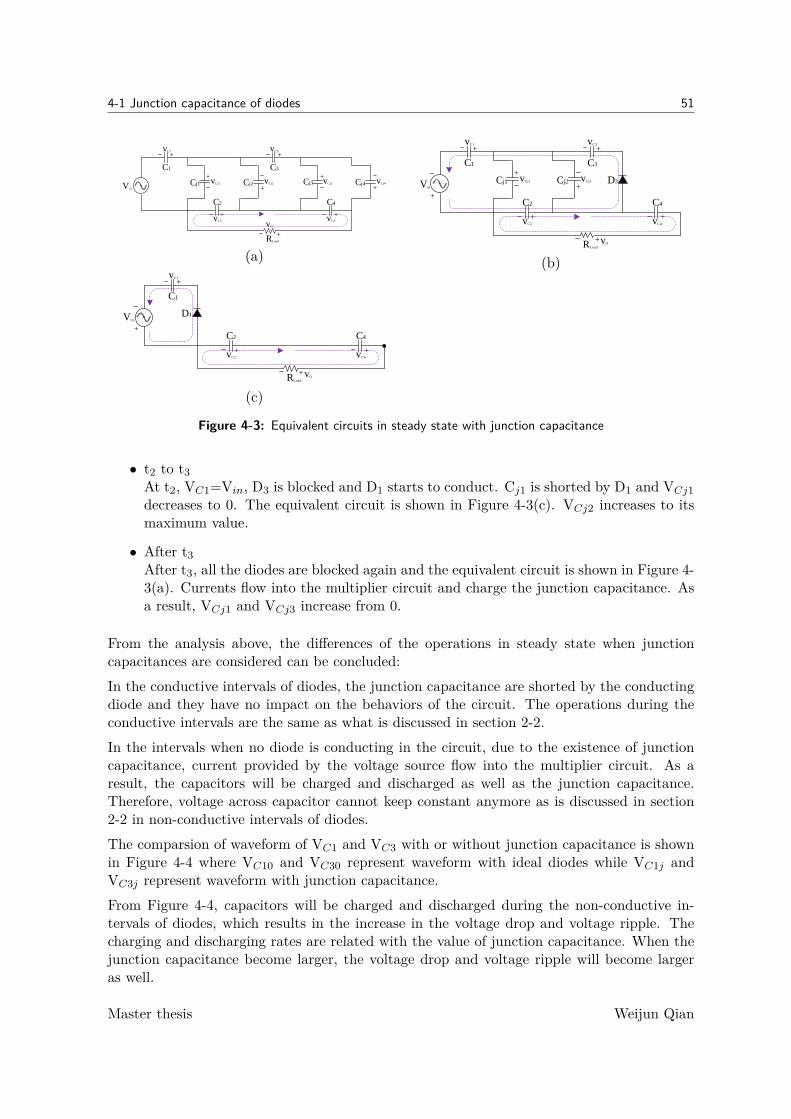
4-1 Junction capacitance of diodes 51
AC
Rload
Vout
C1
C2
C3
C4
D1 D2 D3 D4
+
-
+ +
+ +
- -
- -
+
+
+
+-
-
-
-Cj1 Cj2 Cj3 Cj4
Rload
Vout
C2 C4
D1 D2 D3 D4
+ +
+
- -
- -
+
+
+
+-
-
-
-Cj1 Cj2 Cj3 Cj4
VS
RLoad
vO+
vC1
vC2
vCj1
vC3
vCj2 vCj3
vC4
vCj4
+
+
+
+
+
+
+
+D1 D2 D3 D4
C1
C2
C3
C4
Cj1 Cj2 Cj3 Cj4
Vin
RLoad
vO
+
vC1
vC2
vCj1
vC3
vCj2 vCj3
vC4
vCj4
+
+
+
+
+
+
+
+
C1
C2
C3
C4
Cj1 Cj2 Cj3 Cj4
(a)
AC
Rload
Vout
C1
C2
C3
C4
D1 D2 D3 D4
+
-
+ +
+ +
- -
- -
+
+
+
+-
-
-
-Cj1 Cj2 Cj3 Cj4
Vin
RLoad
vO+
vC1
vC2
vCj1
vC3
vCj2
vC4
+
+
+
+
+
+ D3
C1
C2
C3
C4
Cj1 Cj2
+
(b)
AC
Rload
Vout
C1
C2
C3
C4
D1 D2 D3 D4
+
-
+ +
+ +
- -
- -
+
+
+
+-
-
-
-Cj1 Cj2 Cj3 Cj4
RLoad
vO+
vC1
vC2 vC4
+
+ +
D1
C1
C2 C4
Vin
+
(c)
Figure 4-3: Equivalent circuits in steady state with junction capacitance
• t2 to t3At t2, VC1=Vin, D3 is blocked and D1 starts to conduct. Cj1 is shorted by D1 and VCj1decreases to 0. The equivalent circuit is shown in Figure 4-3(c). VCj2 increases to itsmaximum value.
• After t3After t3, all the diodes are blocked again and the equivalent circuit is shown in Figure 4-3(a). Currents flow into the multiplier circuit and charge the junction capacitance. Asa result, VCj1 and VCj3 increase from 0.
From the analysis above, the differences of the operations in steady state when junctioncapacitances are considered can be concluded:In the conductive intervals of diodes, the junction capacitance are shorted by the conductingdiode and they have no impact on the behaviors of the circuit. The operations during theconductive intervals are the same as what is discussed in section 2-2.In the intervals when no diode is conducting in the circuit, due to the existence of junctioncapacitance, current provided by the voltage source flow into the multiplier circuit. As aresult, the capacitors will be charged and discharged as well as the junction capacitance.Therefore, voltage across capacitor cannot keep constant anymore as is discussed in section2-2 in non-conductive intervals of diodes.The comparsion of waveform of VC1 and VC3 with or without junction capacitance is shownin Figure 4-4 where VC10 and VC30 represent waveform with ideal diodes while VC1j andVC3j represent waveform with junction capacitance.From Figure 4-4, capacitors will be charged and discharged during the non-conductive in-tervals of diodes, which results in the increase in the voltage drop and voltage ripple. Thecharging and discharging rates are related with the value of junction capacitance. When thejunction capacitance become larger, the voltage drop and voltage ripple will become largeras well.
Master thesis Weijun Qian

52 Impact of parasitic components in the circuit
Figure 4-4: Waveform of capacitor voltage with junction capacitance
Simulations are made in LTspice with the existence of the junction capacitances of diodes toverify the theoretical analysis. The junction capacitances are set to be 0, 50pF and 200pF tohave a comparison. The other circuit parameters keep unchanged.
The simulation waveform is shown in Figure 4-5.
Figure 4-5: Simulation waveform with junction capacitance
The values of voltage drop and voltage ripple are shown in Table 4-1.
Due to the existence of junction capacitances, currents will flow into the mutliplier circuitduring non-conductive intervals of diodes and capacitors are charged and discharged as aresult. Therefore, the voltage ripple and voltage drop of capacitors are increased. When thevalues of junction capacitances are larger, the values of voltage drop and voltage ripple getlarger as well. Diodes with low junction capacitance should be chosen to improve the voltageregualtion of the multiplier circuit.
Master thesis Weijun Qian

4-2 Parasitic components of capacitors 53
Table 4-1: Voltage drop and voltage ripple with junction capacitance
Cj Voltage drop/V Voltage ripple/V0 130.7 58.7
50pF 747.8 228.2200pF 2339.3 705.9
4-2 Parasitic components of capacitors
The parasitic components of capacitors include equivalent series resistor(ESR), equivalentseries inductance(ESL) and equivalent parallel capacitance(Cpp) as is shown in Figure 4-6.
C
Cpp
ESLESR
Figure 4-6: Parasitic components of capacitor
The studies are based on the actual capacitor that is used in the 2-stage voltage multipliercircuit, which is MLCC - SMD/SMT 4kV 2200pF 10% X7R from Syfer.
Based on the dissipation factor of the capacitor and the operating frequency, the ESR of eachindividual capacitor can be calculated:
ESR = tanδ ∗ 12πfC = 0.025 ∗ 1
2π ∗ 500000 ∗ 2200 ∗ 10−12 = 3.62Ω
Therefore,the value of the parasitic components for each individual capacitor applied is shownin Table 4-2.
Table 4-2: Parasitic components for each individual capacitor
Capacitor Type ESR ESL CppMLCC - SMD/SMT 4kV2200pF 10% X7R,Syfer 3.62Ω 3nH 1pF
In order to meet the requirements for the capacitance value as well as the voltage rating ofeach individual capacitors, 14 capacitors are connected in parallel as a group and three suchgroups are connected in series in each stage. Therefore, in each stage, 42 capacitors are usedin total. The equivalent values of capacitance, ESR, ESL and Cpp per stage are shown inTable 4-3.
Master thesis Weijun Qian

54 Impact of parasitic components in the circuit
Table 4-3: Equivalent values of parasitic components of capacitors per stage
Capacitance ESR ESL Cpp10.267nF 0.775Ω 0.643nH 4.67pF
4-2-1 Equivalent Series Resistance
In this section, the influence of ESR is discussed. ESR is the electrical resistance in series withthe capacitor plate and ESR is made up of the metal leads and plates and the connectionsbetween them.
There are three effects resulted from ESR in the steady state operations of the voltage multi-plier circuit. The first one is that the current in the circuit is decreased due to the increasedimpedance Z=R- j
ωC compared with the ideal capacitor. The second effect is that when thevoltage source has reached ± Vm, the diode will not stop conducting immediately because ofthe voltage across ESR VESR. The diode continues to conduct in the circuit before VESR isdischarged to 0. The last effect is that ESR will bring additional voltage drop across capaci-torsr. The additional voltage drop caused by ESR can be calculated by ∆ (∆ V)=ESR*Iav[17].
The simulations are made by setting the value of ESR in the simulation model. The voltagedrop caused by ESR is shown in Figure 4-7.
Figure 4-7: Simulation waveform with ESR
Due to fact that VESR will decrease to 0 rapidly when the voltage source reaches its maximumvalue in one switching cycle, phenomena called ’ESR jump’ are present in capacitor voltageas is shown in Figure 4-8.
The existence of ESR has little to do with the voltage ripple. The voltage ripple is causeddue to the existence of the output load. The output capacitors charge the output load andtherefore the voltage ripple exists. Since the ESR of output capacitors are in series withRLoad in the output circuit, the output current is decreased. As a result, the voltage rippleof output capacitors decrease. However, since the value of ESR is so small compared withRLoad, the influence of ESR to voltage ripple is so small that can be neglected.
Discussions:
Master thesis Weijun Qian

4-2 Parasitic components of capacitors 55
Figure 4-8: ESR jump
1.The existence of ESR increases the output voltage drop. The additional voltage drop of thekth capacitor is related with ESR and IC :
∆(∆VCk) = ESRCk ∗ (k∑i=1
ICi)
The additional output voltage drop is the summation of the additional voltage drop acrossall the output capacitors:
∆(∆Vo) =k∑i=1
∆(∆V2i)
2.The influence of ESR to voltage ripple is very slight compared with the voltage drop. Theincrease in voltage ripple can be ignored especially with a small ESR value.
3.The existence of ESR causes the phenomena of ’ESR jump’ in capacitor voltage.
4.The existence of ESR causes extra power losses in the circuit which will be further discussedin chapter 5.
4-2-2 Equivalent Series Inductance
The equivalent series inductance(ESL) is another important parasitic component in a regularelectrolytic capacitor. It represents the inductive property of the capacitor construction. Theexistence of ESL will influence the voltage drop, voltage ripple and circuit stability.
Taking ESL into consideration, the resonance occurs due to the combination of L and C. Theresonance frequency is :
f = 12π√LC
= 12π√
3 ∗ 10−9 ∗ 2.2 ∗ 10−9= 62MHz
The capacitor behaves like an inductor when the operating frequency is over the resonancefrequency 62MHz, which means that the voltage multiplier must be operated at the frequencyunder the resonance frequency. For the selection of capacitors, the ESL must be considered.
Master thesis Weijun Qian

56 Impact of parasitic components in the circuit
Assume the rectifiers are ideal and ESL is not considered, the total reactance per stage isprovided only by the capacitor:
X = XC = − j
2πfC
If the parasitic series inductance of capacitor is taken into consideration, the reactance perstage is decreases:
X = XC +XL = − j
2πfC + j2πfL = j(− 12πfC + 2πfL)
The current value in the voltage multiplier circuit is increased. Voltage across capacitors arecalculated by UC= 1
C
∫Idt, therefore the increase in the current will result in the increase in
capacitor voltage. The voltage drop is smaller and the deduction of the voltage drop is relatedwith the ESL value. ESL has little to do with voltage ripple as well.
Simulations are made in LTspice. The simulation waveform of output voltage with andwithout ESL in steady state are shown in Figure 4-9.
Figure 4-9: Simulation waveform with ESL
The simulation results of voltage drop and voltage ripple are shown in Table 4-4.
Table 4-4: Simulation results with ESL
Voltage drop/V Voltage ripple/VIdeal capacitors 130.7 58.7
Capacitors with ESL 114.9 58.7
The simulation results correspond with the theoretical analysis. The ESL will decrease thevalue of voltage drop and has little to do with voltage ripple.
There are some other interesting phenomena to be paid attention to with the existence ofESL:
1.The existence of ESL results in LC oscillation as is shown in Figure 4-10.
Master thesis Weijun Qian

4-2 Parasitic components of capacitors 57
Figure 4-10: LC oscillation due to ESL
The frequency of LC oscillation is the resonance frequency 62MHz calculated above, whichmeans each individual oscillation takes around 15.9ns. In the simulation results, during0.342us, 21 LC oscillations take place in total. Therefore, each individual LC oscillation take16.2ns, which is correspond with the calculated value of 15.9ns.The LC oscillation will also influence the stability of the voltage multiplier circuit.2.When the diodes are conducting in the circuit, current will flow through ESL and there willbe voltage across ESL u(t)=Ldidt . The voltage induced across ESL is not large, but it willcause voltage spikes in capacitor voltage as is shown in Figure 4-11.
Figure 4-11: Voltage spikes due to ESL
Discussions:1.The existence of ESL will decrease the voltage drop and has little to do with voltage ripple.ESL are in series with capacitor and will decrease the reactance per stage, which results inlarger current and therefore larger voltage across capacitors.2.The combination of ESL and capacitor will cause LC oscillations in the multiplier circuitwhich may influence the stability of the circuit. The oscillation frequency is related with thevalues of ESL and capacitor.3.The voltage across ESL will cause the phenomena of voltage spikes in capacitor voltage.However, due to the relatively low values of ESL and di
dt , the influence of voltage spikes arenot important.
Master thesis Weijun Qian

58 Impact of parasitic components in the circuit
4-2-3 Equivalent parallel capacitance
Besides ESR and ESL, there is another kind of parasitic component for the capacitor whichis not discussed commonly - parasitic parallel capacitance (Cpp). The parasitic parallel ca-pacitance represents the structural capacitance between the capacitance and the ground.
The existence of parasitic parallel capacitance will influence the equivalent value of the capac-itance in each stage. Due to the change of the capacitor value, voltage drop and voltage ripplewill also be impacted by Cpp. The value of the real Cpp is often very small compared withthe real capacitor value, in order to study the influence of Cpp, the value of Cpp is assumed tobe 0.5nF per stage in this section. Therefore, the equivalent capacitor value considering Cppis 10.767nF.
According to equation (2-12) and (2-16), the existence of Cpp will decrease voltage drop andvoltage ripple in the multiplier circuit. The calculation result are shown in Table 4-5.
Table 4-5: Calculation results of voltage regulation with Cpp
Voltage drop/V Voltage ripple/VIdeal capacitors 136.36 58.44
Capacitors with Cpp 130.3 55.73
Therefore, the values of voltage drop and voltage ripple considering Cpp is 95.4% of the valueswhen ideal capacitors are used.
Simulations are made in LTspice. The simulation waveform of output voltage with andwithout Cpp in steady state are shown in Figure 4-12.
Figure 4-12: Simulation waveform of output voltage with Cpp
The simulation results are shown in Table 4-6.
The ratio between the simulated value is :
∆Vo,Cpp∆Vo,ideal
= 122.48128.17 = 95.5%
Master thesis Weijun Qian

4-3 Parasitic components of transformer 59
Table 4-6: Simulation results of voltage regulation with Cpp
Voltage drop/V Voltage ripple/VIdeal capacitors 128.17 56.66
Capacitors with Cpp 122.48 54.04
δVo,CppδVo,ideal
= 54.0456.66 = 95.4%
The simulation results correspond with the theoretical analysis. The existence of Cpp decreasesthe values of voltage drop and voltage ripple.
4-3 Parasitic components of transformer
4-3-1 Influence of parasitic components to the transformer
In the high frequency high voltage power supply circuit, the output of the transformer is theinput of the voltage multiplier circuit. Therefore, the parasitic components of the transformerwill influence the behavior of the voltage multiplier circuit as well. The equivalent circuit ofparasitic components of the transformer is shown in Figure 4-13[18].
RsRp
Cdp CdsRe
Lp Ls
Cmp Cms
Cw
1:n
Figure 4-13: Parasitic components of transformer
In the equivalent circuit, Lp and Ls represent the leakage inductance at primary side andsecondary side of the transformer respectively. Rp and Rs2 represent the dc winding resistancefor the primary and secondary windings while Re is the equivalent core-loss shunt resistance.Cdp and Cds are the winding capacitance at the primary and secondary side, Cmp and Cmsrepresent the distributed capacitance between the core and windings. Cw is the distributedcapacitance between primary winding and secondary winding.
The parasitic components of the transformer especially the leakage inductance and windingcapacitance have great influence on the performance of the voltage multiplier circuit that cannot be ignored. The existence of leakage inductance may cause the delay of the conductionof input current and the stored energy in the leakage inductance will cause voltage spikes.The existence of winding capacitance will result in the current spikes. Leakage inductanceand winding capacitance will also lead to oscillation in the circuit. The input voltage atthe voltage multiplier side will be smaller than estimated and the voltage regulation of themultiplier circuit will be affected as a result.
Master thesis Weijun Qian

60 Impact of parasitic components in the circuit
The definition of the coupling coefficient of a transformer is K= M√L1L2
, where L1,L2 representprimary winding inductance and secondary winding inductance respectively, M is the mutualinductance between the primary and secondary windings. For ideal transformers, the valueof coupling coefficient equals to 1, which means perfect coupling between the primary andsecondary winding that no leakage inductance exists. However, in reality , due to the phys-ical distance between primary and secondary windings, part of the windings behave like aninductor in series with the transformer and therefore the coupling coefficient is smaller than1. The coupling coefficient can also be realized in LTspice by changing the K-statement fortransformer.There are three main effects caused by the parasitic components to the transformer circuit.The first effect is the delay of conduction of current and voltage as is shown in Figure 4-14.The current and voltage at the primary side of the tranformer are Ip and Up respectively.The current and voltage at the secondary side of the tranformer are Is and Us respectively,which are also the input of the voltage multiplier circuit.
Uin
Ip
Up
t1 t2 t3 t4 t5 t6
Uin
Ip,idealIp,actual
t1 t2 t3 t4 t5 t6
t0
t0
Up,ideal
Up,actual
t
t
Figure 4-14: Waveform at primary side of the transformer
In the voltage multiplier circuit with the ideal transformer,Ip increases rapidly at beginningand Up is in phase with the input voltage for the transformer. When the parasitic componentsof the transformer are considered,the conduction of Ip is delayed due to the effect of leakageinductance as is shown in Figure 4-14. The currents flow through the leakage inductance andestablish a magnetic field. When the currents change, the flux change and the changing fluxinduce EMF. The induced EMF causes a current that opposes Ip. Therefore, the built-up ofIp is slower than the ideal transformer circuit and no current spikes occur at the beginning.As a result, the built up of Up lags the input voltage source when parasitic components ofthe transformer are considered.
Master thesis Weijun Qian

4-3 Parasitic components of transformer 61
The second effect is that the errors of the voltage turn ratio from primary side to secondary sideoccur because of the winding resisitances, leakage flux and displacement currents, which arepresented by leakage inductance and winding capacitance[19]. The comparison of waveformfor Us is shown in Figure 4-15.
Us
t
Us,ideal
Us,actual
Figure 4-15: Comparsion of waveform for Us
The third effect is that the leakage inductance and distribution capacitance will lead to LCoscillation in the circuit as well, which may result in the electromagnetic interference.
4-3-2 Influence to the electrical performance of multiplier circuit
As is discussed in section 2-1, D4 starts to conduct when Vin increases to the value that fulfillsthe condition VC1+VC3+Vin = VC2+VC4. Due to the fact that the maximum value of Vinis decreased as is shown in Figure 4-15, it can be inferred that the boost of voltages acrosscapacitors will end earlier in start-up process with actual transformer models than with theideal models. Therefore, the steady state is reached earlier.
Based on the fact that the start-up process is forced to end earlier, it can be inferred thatthe voltage drop of the multiplier circuit is increased while the voltage ripple is decreased.However, it is difficult to calculate the voltage drop and voltage ripple caused by parasiticcomponents of the transformer theoretically.
Simulations are made in LTspice to verify the theoretical analysis. The leakage inductance isset as µH, the winding capacitance is set as 3nF and the coupling coefficient is set as 0.98.The simulation waveform of output voltage with and without parasitic components of thetransformer are shown in Figure 4-16.
The voltage drop and voltage ripple are shown in Table 4-7.
Table 4-7: Simulation results of voltage regulation with actual transformer
Voltage drop Voltage rippleIdeal transformer 120.9V 55.7VActual transformer 1.902kV 45.2V
Due to the sudden stop of the start-up process caused by the decreased input voltage, thesteady state is reached earlier and therefore the rise time will be shorter than the ideal case.The decay process has little to do with the parasitic components of the transformer. The
Master thesis Weijun Qian

62 Impact of parasitic components in the circuit
Figure 4-16: Simulation waveform of output voltage with actual transformer
reduced steady state output voltage value may decrease the decay time but the influence isnot obvious.
The simulation waveform of rise time and decay time with and without parasitic componentsof the transformer are shown in Figure 4-16 and Figure 4-17 respectively.
Figure 4-17: Simulation waveform of decay process with actual transformer
The simulation results of rise time and decay time are shown in Table 4-8.
The simulation results correpsond with theoretical analysis. The parasitic components oftransformer will decrease the value of input voltage for the multiplier circuit. As a result, thevoltage drop is increased and the voltage ripple is decreased. The rise time is decreased aswell. The parasitic components of transformer has little to do with the decay time.
Master thesis Weijun Qian

4-4 Summary 63
Table 4-8: Simulation results for respond time with actual transformer
Rise time Decay timeIdeal transformer 26.37µs 5.23msActual transformer 16.06µs 5.22ms
4-4 Summary
In this chapter, the impact of important parasitic components of diodes, capacitors andtransformer are considered.
The junction capacitance of diodes will increase voltage drop and voltage ripple as is analyzedin section 4-1. The influence of ESR, ESL and Cpp of capacitors are discussed in section 4-2.The existence of ESR will increase voltage drop and cause ’ESR jump’. The existence of ESLwill decrease voltage drop and cause LC oscillations and voltage spikes in the circuit. Theexistence of Cpp will increase the equivalent capacitance value per stage and decrease voltagedrop and voltage ripple. The parasitics of the transformer will force the start-up process toend earlier than expected. As a result, the voltage drop is increased, the voltage ripple isdecreased and the rise time is decreased as well.
In the next chapter, power losses in the multiplier circuit are discussed, which is anotherimportant criteria to evaluate the voltage multiplier circuit.
Master thesis Weijun Qian

64 Impact of parasitic components in the circuit
Master thesis Weijun Qian

Chapter 5
Power Loss Analysis of the MultiplierCircuit
Besides the electrical performance of the voltage multiplier circuit, the power loss analysis isalso significant in order to reduce heating and prolong the service life of the power supplycircuit. Therefore, the power losses in the multiplier circuit are discussed in this chapter.
The power losses mainly come from the conduction loss and reverse recovery loss of diodesand ESR of capacitors. In section 5-1, detailed switching process of diodes is analyzed. Theformulas to calculate the currents in the multiplier circuit are derived in section 5-2. Thepower losses caused by diodes and capacitors are calculated respectively in section 5-3 and5-4.
5-1 Detailed switching process of diodes in HWCW voltage mul-tiplier
In the real voltage multiplier circuit, reverse recovery will take place during the switchingprocess of diodes, which results in the diode switching losses and therefore cannot be ne-glected. In this section, the reverse recovery problems are taken into consideration and thedetailed analysis of the switching process of diodes in the HWCW voltage multiplier circuitare discussed.
The waveform of current through ideal diodes without reverse recovery in steady state isshown in Figure 2-6. The waveform of the diode currents in steady state taking reverserecovery problems into consideration are shown in Figure 5-1. The operations in the positiveswitching cycles of the input voltage source when even diodes are conducting in the circuit areexplained as an example. The operations of the odd diodes in the negative switching cyclesare the same. The reverse recovery procedure of diodes in the first stage and diodes in theother stages are very different[20].
1. Reverse recovery of diodes in the first stage:
Master thesis Weijun Qian

66 Power Loss Analysis of the Multiplier Circuit
Uin,ID
t1 t3t2
ID2
ID4
Uin
t4t2 t
Figure 5-1: Reverse recovery of diodes in steady state
• t2 to t3From t2 to t3, the operations are the same as is discussed in section 2-2-1. D2 starts toconduct at t2. ID2 decreases to 0 at t3 when Uin increases to Vm.
• t3 to t4From t3 to t4, the reverse recovery procudure of D2 occurs. The equivalent circuitis shown in Figure 5-2(a). In order to eliminate the minor carrier stored in D2, thereverse recovery procedure of D2 begins. ID2 will turn negative and increase to themaximum reverse recovery current ID2rrm at first. Then ID2 will decrease to 0 at t4.The voltage across D2 is zero since VD2=VC1ss,min+Vm-VC2ss,max. Therefore, the zerovoltage switching(ZVS) is realized.
2. Reverse recovery of diodes in the other stages
• t1 to t′2From t1 to t′2, the operations are the same as is discussed in section 2-2-1. ID4 decreasesto zero and VC4=VC3 at t2.
• t′2 to t3From t′2 to t3, D2 is conducting in the circuit. The equivalent circuit is shown inFigure 5-2(b), VD4 equals to the forward voltage drop of D2 as VC4 and VC3 stop tochange. Therefore, D4 is not blocked and ID4=0.After t3, D4 is blocked. Since ID4 has been zero, zero current switch is realized and noreverse recovery takes place.
Therefore, the reverse recovery process only occurs in the diodes in the first stage(D2 andD2). However, even though the reverse recovery occurs, the reverse recovery loss is zero dueto the zero voltage switching. Diodes in other stages have no reverse recovery losses.
The simulation are made in LTspice with the actual model of power rectifier Byg23m. Thesimulation waveform is shown in Figure 5-3.
Discussions:
In the simulation waveform shown in Figure 5-3, D4 still shows reverse recovery process. Thisis because of the commutation of diode currents as is shown in the time interval from t2
Master thesis Weijun Qian

5-2 Derivations of diode currents 67
AC
Rload
Vout
C1
C2
C3
C4
D1 D2 D3 D4
+
-
+ +
+ +
- -
- -
C1
C2 C4
RLoad
D2
vO
Vin
+
vC1
+
vC2
+ vC4
+
id2
(a)
Rload
Vout
C1
C2
C3
C4
D1 D2 D3 D4
+
-
+ +
+ +
- -
- -
AC
C1 C3
C2 C4
RLoad
D2 D4
vO
Vin
+
vC1
+vC3
+
vC2
+ vC4
+
(b)
Figure 5-2: Equivalent circuits of reverse recovery procedures
Figure 5-3: Simulation results of actual diode models
to t′2 in Figure 5-1. In the theoretical analysis, the commutations of diode currents are nottaken into consideration , VC3 and VC4 are assumed to keep constant after they have reachedthe same value. When the actual diode models are applied, D2 starts to conduct before ID4decreases to 0. As a result, VC3 continues to decrease and VC4 continues to increase until t′2after they have reached the same value. Therefore, VC4>VC3 when ID4 decreases to 0. Asa result, negative voltage is applied across D4 and ID4 turns to a small negative value. Thereverse recovery of D4 can be ignored compared with that of D2.
5-2 Derivations of diode currents
In order for further research on power losses, the method to calculate currents in the HWCWvoltage multiplier circuit is derived in this section.
From the analysis above, diodes with odd numbers and diodes with even numbers conduct indifferent half switching cycles of the input voltage source. Moreover, diodes with higher stagenumbers conduct at first and diodes with lower stage numbers conduct at last. When thekth diode is conducting in the circuit, all the capacitors with numberleqslantk are chargingor discharging in the multiplier circuit. Therefore, the total charging and discharging timeof diodes in low stages are longer than diodes in high stages. From the equation of thevoltage ripple of each capacitor shown in equation (2-9) , it can be obtained the differenceof the voltage ripple of two adjacent odd/even capacitors is Io
fC assuming the capacitancedistribution is equal in each stage.
Master thesis Weijun Qian

68 Power Loss Analysis of the Multiplier Circuit
The voltage drop across capacitors are:
∆V2k−1 = (2n− k + 2)(k − 1) ∗ IofC
(5-1)
∆V2k = [(2n− 1)(n+ 1)− k2] ∗ IofC
(5-2)
The input voltage source of the multiplier circuit is Asin2πft, where A is the maximum inputvoltage value Vm.
• Derivation of ID1When D1 is conducting in the circuit, ID1=Is=IC1.The maximum value of VC1 in steady state is A. According to the regulations concludedin section 2-1-2, the equation can be obtained:
Asin2πft = A− (δVC1 − δVC3) = A− IofC
(5-3)
t =arcsin(1− Io
AfC )2πf (5-4)
Equation (5-4) is the time point when D1 starts to conduct. The conduction of D1 stopsat the time point when Vin reaches -Vm. Therefore, the conducting time for D1 is:
tD1 = 14f −
arcsin(1− IoAfC )
2πf (5-5)
This is also the charging time of C1 during the conduction of D1. Therefore, ID1 canbe calculated:
ID1 = IC1 = C1dV
dt= C1
IofC
tD1= IoftD1
= Io
14 −
arcsin(1− IoAfC
)2π
(5-6)
This is the average value of ID1 during tD1, the average value and rms value in oneswitching period can be calculated based on ID1, tD1 and frequency.
• Derivation of ID2k−1D2k−1 starts to conduct at the time point when the voltage source reaches the value atwhich fulfills the condition:
Vin +k−1∑i=1
VC2i =k∑i=1
VC2i−1 (5-7)
The equation can be rewritten:
Vin =k∑i=1
VC2i−1 −k−1∑i=1
VC2i = VC2k−1 +k−1∑i=1
(VC2i−1 − VC2i) (5-8)
Master thesis Weijun Qian

5-2 Derivations of diode currents 69
Vin = VC2k−1 + VC1 − VC2 +k−1∑i=2
(VC2i−1 − VC2i) (5-9)
The difference of the odd and even number capacitor in the ith stage (i<k) is:2i∗IofC
At the time point when D2k−1 starts to conduct, the value of VC1,VC2 and VC2k−1 are:
VC1 = A− kIofC
(5-10)
VC2 = 2A−∆VC2 −(n− k)Io
fC= 2A− (2n− k)Io
fC(5-11)
VC2k−1 = 2A−∆VC2k−1 −IofC
= 2A− (2n− k + 2)(k − 1) ∗ IofC− IofC
(5-12)
Therefore, the equation can be obtained:
Asin2πft = A− (2nk − 4n− 2k2 + 8k − 3) IofC
(5-13)
Let the corfficient to be α2k−1=2nk-4n-2k2+8k-3
t =arcsin(1− α2k−1Io
fCA )2πf (5-14)
This is the time from the time point at which D2k−1 starts to conduct to the time pointwhen Vin reaches -Vm. The conduction of D2k−1 stops at the time point when VC2k−1reaches its maximum value in steady state. Then, odd diode in one stage lower startsto conduct. Therefore, the conducting time of D2k−1 should be:
tD2k−1 = 14f −
arcsin(1− α2k−1IofCA )
2πf −k−1∑i=1
tD2k−1 (5-15)
The current during the conduction of D2k−1 is:
ID2k−1 = IC2k−1 = C2k−1dV
dt= C
IofC
tD2k−1= IoftD2k−1
= Io
f ∗ ( 14f −
arcsin(1−α2k−1IofCA
)2πf −
∑k−1i=1 tD2k−1)
(5-16)
This is the average value of ID2k−1 during the conduction of D2k−1, the average valueand rms value of ID2k−1 in one switching period can be calculated based on ID2k−1,tD2k−1 and frequency.In order to calculate the diode currents in the circuit, the calculation should start fromrectifiers in the lower stages at first.
Master thesis Weijun Qian

70 Power Loss Analysis of the Multiplier Circuit
• Derivation of ID2kD2k starts to conduct at the time point when the voltage source reaches the value atwhich fulfills the condition:
Vin +k∑i=1
VC2i−1 =k∑i=1
VC2i (5-17)
The equation can be rewritten:
Vin =k∑i=1
VC2i −k∑i=1
VC2i−1 = VC2 − VC1 +k∑i=2
(VC2i − VC2i−1) (5-18)
At the time point when D2k starts to conduct, the value of VC1,VC2 are:
VC1 = A− (n− k)IofC
(5-19)
VC2 = 2A−∆VC2 −kIofC
= 2A− (n+ k)IofC
(5-20)
In the same stage, VC2i−1>VC2i
k∑i=2
(VC2i − VC2i−1) =k−1∑i=1
2i IofC
= −k(k − 1)IofC
(5-21)
Therefore, the equation can be obtained:
Asin2πft = A− k(k + 1)IofC
(5-22)
t =arcsin(1− k(k+1)Io
fCA )2πf (5-23)
This is the time from the time point at which D2k starts to conduct to the time pointwhen Vin reaches Vm. The conduction of D2k stops at the time point when VC2kreaches its maximum value in steady state. Then, even diode in one stage lower startsto conduct. Therefore, the conducting time of D2k should be:
tD2k = 14f −
arcsin(1− k(k+1)IofCA )
2πf −k−1∑i=1
tD2k (5-24)
The current during the conduction of D2k−1 is:
ID2k = IC2k = C2kdV
dt= C
IofC
tD2k= IoftD2k
= Io
f ∗ ( 14f −
arcsin(1− k(k+1)IofCA
)2πf −
∑k−1i=1 tD2k)
(5-25)
Master thesis Weijun Qian

5-2 Derivations of diode currents 71
This is the average value of ID2k during the conduction of D2k, the average value andrms value of ID2k in one switching period can be calculated based on ID2k, tD2k andfrequency.In order to calculate the diode currents in the circuit, the calculation should start fromrectifiers in the lower stages at first.
Using the equation (5-6),(5-16) and (5-25), the diode currents can be calculated. In case ofideal diode models, the model shown in Figure 5-4 can be used when calculating the RMSvalue of currents taking ID1 and ID3 as an example. The commutations between the currentsand the rise time of currents are ignored.
Figure 5-4: RMS calculation model
In the RMS current model, tD3 and tD1 represent the time when D3 and D1 start to conductin the circuit in steady state, T is the time when the voltage source reaches -Vm.
The calculation results of tD and ID are shown in Table 5-1.
Table 5-1: Calculation results of tD and ID
D1 D2 D3 D4tD/µs 0.028 0.04 0.035 0.03ID/A 7.022 4.964 5.667 6.759
The calculation values of average and RMS values of currents are shown in Table 5-2.
Table 5-2: Calculation results of avetage and rms values of diode currents
D1 D2 D3 D4ID,av/mA 98.3 99.28 95.39 101.38ID,rms/mA 968.23 815.8 745.24 838.7
Simulations are made in LTspice to verify the calculations. The comparison of the calculationand simulation results of diode currents are shown in Table 5-3.
From the comparison between the simulation and calculation results of diode currents shown inTable 5-3, the calculation results of ID1 and the even diodes correspond with the simulationresults. However, the calculation of ID3 has errors of around 10%. This is because of theinfluence of the output loop that even capacitors are always charging the output load inthe whole switching cycle. As a result, when the odd diodes start to conduct, the voltage
Master thesis Weijun Qian

72 Power Loss Analysis of the Multiplier Circuit
Table 5-3: Comparison of simulation and calculation results of diode currents
ID,av,sim/mA ID,av,cal/mA Errors ID,rms,sim/mA ID,rms,cal/mA ErrorsD1 99.08 98.3 0.8% 951.5 968.23 1.76%D2 99.3 99.28 0.02% 804.37 815.8 1.42%D3 101.54 95.39 6.01% 845.69 745.24 11.88%D4 101.9 101.38 0.51% 826.52 838.7 1.47%
across even capacitors will be smaller than the maximum steady state value and the voltageacross odd capacitors will be larger than the minimum steady state value. Therefore, someoptimizations can be applied to improve the accuracy of the calculation of odd diode currentsby considering the effect of the output loop.The output loop is the RC discharging circuit. The time constant is τ=CRL
n =1000µs. Dueto the conduction time of diodes is much smaller than the switching cycle tDT, the voltagedrop of C2 between the end of conduction of even diodes and beginning of conduction of odddiodes can be seen as the voltage drop of C2 in half of a switching cycle.
∆VC3 = (1− exp(− tτ
)Vss) = (1− exp(−0.001)) ∗ 9960 = 9.955V
Asin2πft+ 2A− 2IofC− 9.955 = A− 2Io
fC+ 2A− 4Io
fC− kIofC
+ 9.955
Asin2πft = A− 5IofC
+ 19.91
As a result, tD3=0.029µs,ID3=6.897A and ID3,av=100mA, ID3,rms=847.6mA after optimiza-tion.The comparison between calculation and simulation results after optimization is shown inTable 5-4.
Table 5-4: Comparison of simulation and calculation results of diode currents after optimization
ID,av,sim/mA ID,av,cal/mA Errors ID,rms,sim/mA ID,rms,cal/mA ErrorsD1 99.08 98.3 0.8% 951.5 968.23 1.76%D2 99.3 99.28 0.02% 804.37 815.8 1.42%D3 101.54 100 1.5% 845.69 847.6 0.23%D4 101.9 101.38 0.51% 826.52 838.7 1.47%
Discussions:Formulas to calculate the diode currents in the HWCW voltage multiplier circuit are derived inequation (5-6),(5-16) and (5-25). The optimization method of odd diode currents consideringthe influence of the output load is introduced as well. Based on the diode currents, the averageand rms values of currents through diodes and capacitors can be calculated.The errors between the simulation and calculation results may come from the fact that theoutput current used in the formula is not accurate due to the existence of output load. Whencalculating the average values and rms values , the current is assumed to be discrete butactually it is continuous which will also result in the errors.
Master thesis Weijun Qian

5-3 Conduction losses of diodes 73
5-3 Conduction losses of diodes
In this section, the power losses of the diodes in the voltage multiplier circuit are calculatedand the influence of frequency to power losses is compared. The power losses of diodesconsist of conduction losses and switching losses. The conduction losses are losses producedby diodes during conduction and the switching losses of diodes are caused by reverse recoveryas is discussed in section 5-1.
The conduction loss is calculated by[21]:
Pcon = UD0 ∗ IF,av +RD ∗ I2F,rms (5-26)
Where UD0 is the on-state zero-current voltage and RD is the on-state resistance of the diode.
The diodes used in the real multiplier circuit are GB01SLT12_25C. From datasheet, UD0and RD can be calculated: UD0=0.97V,RD=0.6Ω. The parameters of the voltage multipliercircuit are shown in Table 2-1, the power losses are calculated under three different frequenciesof 100kHz, 250kHz and 500kHz.
Using Equation (5-6),(5-16) and (5-25), the calculation results of diode currents are shown inFigure 5-5.
Table 5-5: Diode currents under different frequencies
Frequency Current D1 D2 D3 D4
100kHz ID,av,cal/mA 100.35 99.63 99.18 98.18ID,rms,cal/mA 652.97 539.97 521.03 547.28
250kHz ID,av,cal/mA 99.28 99.98 99.13 99.96ID,rms,cal/mA 815.8 686.88 675.6 690.47
500kHz ID,av,cal/mA 98.3 99.28 100 101.38ID,rms,cal/mA 968.23 815.8 847.6 838.7
Based on the current values, the conduction losses can be estimated under different frequen-cies. In order to satisfy the maximum peak reverse voltage of the diodes, 10 diodes areconnected in series in each stage to avoid the diodes from breaking down. The conductionlosses are shown in Table 5-6.
Table 5-6: Calculation results of conduction losses
Frequency PD1,cal/W PD2,cal/W PD3,cal/W PD4,cal/W PDtotal,cal/W100kHz 3.53 2.71 2.59 2.75 11.58250kHz 4.96 3.8 3.7 3.83 16.29500kHz 6.58 4.96 5.28 5.2 22.02
Simuations are made in LTspice. The simulation results of diode currents and power lossesbased on the simulation values are shown in Table 5-7 and Table 5-8.
The errors between the calculation results and the simulation results of conduction losses areshown in Table 5-9.
Master thesis Weijun Qian

74 Power Loss Analysis of the Multiplier Circuit
Table 5-7: Simulation results of diode currents under different frequencies
Frequency Current D1 D2 D3 D4
100kHz ID,av,sim/mA 109.14 103.66 107.5 102.72ID,rms,sim/mA 620.22 532.63 527.26 527.03
250kHz ID,av,sim/mA 120.79 118 124.43 119.38ID,rms,sim/mA 747.77 643.27 648.6 607.81
500kHz ID,av,sim/mA 99.08 99.3 101.54 101.9ID,rms,sim/mA 951.5 804.37 845.69 826.52
Table 5-8: Simulation results of conduction losses under different frequencies
Frequency PD1,sim/W PD2,sim/W PD3,sim/W PD4,sim/W PDtotal,sim/W100kHz 3.37 2.65 2.71 2.66 11.39250kHz 4.53 3.63 3.73 3.38 15.27500kHz 6.39 4.85 5.28 5.09 21.61
The conduction losses are related with the selection of diodes and the current values in themultiplier circuit. Diodes with lower UD0 and RD will result in fewer conduction losses. Whenthe diodes and the topology of the multiplier circuit are determined, the conduction lossesare increased with the increased operating frequency since the current is increased.
Table 5-9: Comparison of simulation and calculation results of conduction losses
Frequency Pcon,cal/W Pcon,sim/W Errors100kHz 11.58 11.39 1.7%250kHz 16.29 15.27 6.7%500kHz 22.02 21.61 1.9%
5-4 Power losses of capacitors
The power losses of capacitors are provided by the ESR of capacitors. The ESR is relatedwith the operating frequency in the circuit. Capacitor losses are calculated by:
PC = ESR ∗ I2C,rms (5-27)
The ESR values under different frequencies per stage are shown in Table 5-10.
Capacitor losses are calculated under three different frequencies: 100kHz, 250kHz and 500kHzas well in order to find the influence of frequency to power losses of capacitors. The currentsthrough capacitors are the sum of the diode currents. The capacitor with lower number haslarger charging and discharging time and larger current. The calculation results of capacitorcurrents and power losses are shown in Table 5-11.
Simuations are made in LTspice. The simulation results of capacitor currents and losses basedon the simulation values are shown in Table 5-12.
Discussions:
Master thesis Weijun Qian

5-4 Power losses of capacitors 75
Table 5-10: ESR values under different frequencies
Frequency 100kHz 250kHz 500kHzESR/Ω 3.875 1.55 0.775
Table 5-11: Calculation results of capacitor currents and losses with different frequencies
100kHz 250kHz 500kHz
C1IC1,cal/A 1.13 1.43 1.75PC1,cal/W 4.94 3.16 2.37
C2IC2,cal/A 0.93 1.18 1.45PC2,cal/W 3.35 2.15 1.62
C3IC3,cal/A 0.75 0.96 1.17PC3,cal/W 2.17 1.42 1.06
C4IC4,cal/A 0.54 0.69 0.83PC4,cal/W 1.12 0.73 0.53
PCtotal,cal/W 11.58 7.46 5.58
1.From both the calculation and simulation results, the increase in frequency will result inthe decrease in capacitor losses. When the operating frequency is increased, although therms values of the capacitor current are also increased, the frequency-related ESR values aredecreased and they are in inverse proportion to frequency. As a result, the capacitor lossesare decreased as the frequency is increased.
2.When the frequency is relatively low, the ratio of diode losses is low and the ratio of capacitorlosses is high. When the frequency is relatively high, the ratio of diode losses is high and theratio of capacitor losses is low. The comparison between the diode losses and capacitor lossesare shown in Figure 5-5.
Figure 5-5: Power losses of diodes and capacitors with different frequencies
Master thesis Weijun Qian

76 Power Loss Analysis of the Multiplier Circuit
Table 5-12: Simulation results of capacitor currents and losses with different frequencies
100kHz 250kHz 500kHz
C1IC1,sim/A 1.13 1.42 1.75PC1,sim/W 4.94 3.13 2.37
C2IC2,sim/A 0.91 1.14 1.46PC2,sim/W 3.21 2.01 1.65
C3IC3,sim/A 0.72 0.89 1.22PC3,sim/W 2.01 1.23 1.15
C4IC4,sim/A 0.51 0.6 0.83PC4,sim/W 1.01 0.56 0.53
PCtotal,sim/W 11.17 6.93 5.7Errors 3.7% 7.1% 2.1%
Therefore, when the multiplier circuit is operating at low frequencies, the capacitor lossesshould be considered first. On the contrary, when the operating frequency of the circuit ishigh, the diode losses should be considered first. The choice of frequency should be determinedby taking both the capacitor losses and diode losses into consideration.
5-5 Summary
In this chapter, the main power losses in the voltage multiplier circuit are analyzed. Theservice life of the voltage multiplier circuit can be predicted by considering the power lossanalyses when designing a voltage multiplier circuit.
The detailed switching process of diodes is explained in section 5-1. Reverse recovery onlyoccurs in the diodes in the first stage. Even though the reverse recovery process occurs, dueto the zero voltage switching, the reverse recovery losses of diodes do not exist. Equations fordiode currents are derived and a new RMS value calculation model is proposed in section 5-2.Based on the derivations of diode currents, the conduction losses of diodes and ESR lossesof capacitors can be calculated in section 5-3 and section 5-4 respectively. As the operatingfrequency increases, the conduction losses increase while the ESR losses decrease.
Master thesis Weijun Qian

Chapter 6
Optimization of Capacitance Network
6-1 Introduction
The analyses in the previous chapters are based on the assumption of equal capacitancedistribution per stage in the HWCW voltage multiplier circuit. However, according to [11][12],the performance of voltage drop and voltage ripple will be different when different capacitancesare used per stage. The formulas of output voltage ripple and output voltage drop are shownin equation (6-1) and (6-2) when capacitances are unequal[14]:
δVo = Iof
n∑k=1
n− k + 1C2k
(6-1)
∆Vo = Iof
(n∑k=1
(n− k + 1)2
C2k−1+n−1∑k=1
(n− k + 1)(n− k)C2k
) (6-2)
Table 6-1: Optimization methods for unequal capacitance distribution
Method 1 C2k−1=C2k=C (k>0)Method 2 C1=2C; Ck=C (k>1)Method 3 C2k−1=C2k=(n-k+1)C (k>0)Method 4 C2k−1=(n-k+1)2C; C2k=(n-k+1)C (k>0)Method 5 C2k−1=(n-k+1)2C; C2k=(n-k+1)(n-k)C; C2=C1=C (k>1)
In this section, the electrical performances of the HWCW voltage multiplier circuit includ-ing the voltage regulation, respond time and power losses are studied based on unequalcapacitance distribution per stage. In order to compare the effects of unequal capacitancedistributions, five optimization methods shown in Table 6-1 are discussed. In Table 6-1, Crepresents the base capacitance and C=10nF in this project.
Method 1 to Method 4 in Table 6-1 are proposed by [11] and Method 5 is proposed in thisthesis. The aims of the optimization methods are to decrease the contributions of the terms
Master thesis Weijun Qian

78 Optimization of Capacitance Network
in equation(6-1) and (6-2) to voltage drop and voltage ripple. Moreover, by the proposingof Method 5, the terms in equation (6-1) and (6-2) are minimized to the minimum degree asis shown in equation (6-3) and (6-4) below. The values of output voltage drop and voltageripple are decreased by applying the capacitance distribution methods indicated in Table 6-1.
δVo = IofC
n∑k=1
1(n− k) (6-3)
∆Vo = Iof
(n∑k=1
1C
+n−1∑k=1
1C
) = (2n− 1) IofC
(6-4)
When the stage number of the HWCW voltage multiplier circuit equals to two, the capacitancedistributions of Case 4 and Case 5 are totally the same in each stage. Therefore, the analysesare based on the 3-stage HWCW voltage multiplier shown in Figure 6-1 in this chapter.
C1 C3
C2 C4
RLoad
D1 D2 D3 D4Vin
C6
D5
C5
D6
Figure 6-1: 3-stage HWCW voltage multiplier circuit
The capacitance value in each stage for the five optimization methods are shown in Table 6-2.The capacitance values are selected based on the fact that the total numbers of capacitorsused in each method are kept the same. As a result, the capacitance distrubtion methods arecompared under same size and cost of the multiplier circuit.
Table 6-2: Capacitance distribution values in five optimization methods
C1/nF C2/nF C3/nF C4/nF C5/nF C6/nFMethod 1 35.2 35.2 35.2 35.2 35.2 35.2Method 2 66 33 33 33 33 33Method 3 52.8 52.8 35.2 35.2 17.6 17.6Method 4 118.8 39.6 52.8 26.4 13.2 13.2Method 5 99 66 44 22 11 11
The influence of the optimization methods to voltage drop&voltage ripple, rise time&decaytime and power losses are discussed in section 6-2,6-3 and 6-4 respectively.
6-2 Influence of capacitance optimization to voltage drop and volt-age ripple
As is mentioned in section 2-3-1, the assumptions during the derivations of voltage drop andvoltage ripple are still valid. Therefore, the output voltage drop and voltage ripple of five
Master thesis Weijun Qian
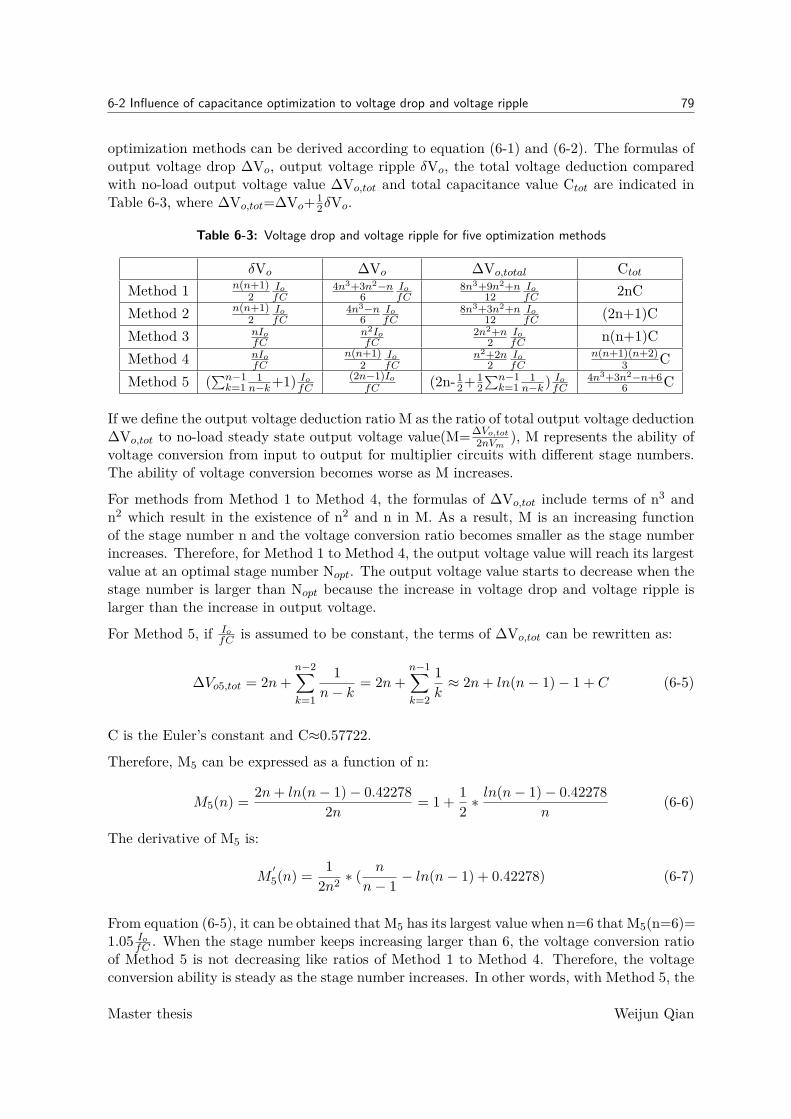
6-2 Influence of capacitance optimization to voltage drop and voltage ripple 79
optimization methods can be derived according to equation (6-1) and (6-2). The formulas ofoutput voltage drop ∆Vo, output voltage ripple δVo, the total voltage deduction comparedwith no-load output voltage value ∆Vo,tot and total capacitance value Ctot are indicated inTable 6-3, where ∆Vo,tot=∆Vo+1
2δVo.
Table 6-3: Voltage drop and voltage ripple for five optimization methods
δVo ∆Vo ∆Vo,total CtotMethod 1 n(n+1)
2IofC
4n3+3n2−n6
IofC
8n3+9n2+n12
IofC 2nC
Method 2 n(n+1)2
IofC
4n3−n6
IofC
8n3+3n2+n12
IofC (2n+1)C
Method 3 nIofC
n2IofC
2n2+n2
IofC n(n+1)C
Method 4 nIofC
n(n+1)2
IofC
n2+2n2
IofC
n(n+1)(n+2)3 C
Method 5 (∑n−1k=1
1n−k+1) IofC
(2n−1)IofC (2n-1
2+12∑n−1k=1
1n−k )
IofC
4n3+3n2−n+66 C
If we define the output voltage deduction ratio M as the ratio of total output voltage deduction∆Vo,tot to no-load steady state output voltage value(M=∆Vo,tot
2nVm ), M represents the ability ofvoltage conversion from input to output for multiplier circuits with different stage numbers.The ability of voltage conversion becomes worse as M increases.
For methods from Method 1 to Method 4, the formulas of ∆Vo,tot include terms of n3 andn2 which result in the existence of n2 and n in M. As a result, M is an increasing functionof the stage number n and the voltage conversion ratio becomes smaller as the stage numberincreases. Therefore, for Method 1 to Method 4, the output voltage value will reach its largestvalue at an optimal stage number Nopt. The output voltage value starts to decrease when thestage number is larger than Nopt because the increase in voltage drop and voltage ripple islarger than the increase in output voltage.
For Method 5, if IofC is assumed to be constant, the terms of ∆Vo,tot can be rewritten as:
∆Vo5,tot = 2n+n−2∑k=1
1n− k
= 2n+n−1∑k=2
1k≈ 2n+ ln(n− 1)− 1 + C (6-5)
C is the Euler’s constant and C≈0.57722.
Therefore, M5 can be expressed as a function of n:
M5(n) = 2n+ ln(n− 1)− 0.422782n = 1 + 1
2 ∗ln(n− 1)− 0.42278
n(6-6)
The derivative of M5 is:
M′5(n) = 1
2n2 ∗ ( n
n− 1 − ln(n− 1) + 0.42278) (6-7)
From equation (6-5), it can be obtained that M5 has its largest value when n=6 that M5(n=6)=1.05 Io
fC . When the stage number keeps increasing larger than 6, the voltage conversion ratioof Method 5 is not decreasing like ratios of Method 1 to Method 4. Therefore, the voltageconversion ability is steady as the stage number increases. In other words, with Method 5, the
Master thesis Weijun Qian

80 Optimization of Capacitance Network
voltage multiplier circuit is able to provide any output voltage in principle even the voltagedrop and voltage ripple are taken into consideration.The voltage conversion ratio Vo
Vmis calculated for the five optimization methods when the
stage number increases from 1 to 15. The results of the voltage conversion ratio are shown inFigure 6-2.
Figure 6-2: Voltage conversion ratio with stage number in 5 methods
From Figure 6-2, it is verified that the voltage conversion ratio of Method 5 can be regardedas constant while the ratios of other methods decrease as the stage number increases. Method5 provides the best performance in voltage drop and votlage ripple whatever the stage numberis. Compared with Method 1 and Method 2, the variations in voltage conversion ratios ofMethod 3,4 are smaller. However, the improvement in voltage drop and voltage ripple willlead to larger total capacitance as a result.The 3-stage HWCW voltage multiplier in Figure 6-1 is used as a case study in this chapter.The values of voltage drop and voltage ripple are calculated with the five optimization methodsas shown in Table 6-4. The base capacitance is C=10nF and other parameters keep unchangedas shown in Table 2-1.
Table 6-4: Calculation results of voltage regulation in 5 methods
Method 1 Method 2 Method 3 Method 4 Method 5δVo,cal/V 22.73 24.24 22.73 30.3 30.3∆Vo,cal/V 83.33 70.71 68.18 60.61 60.61
The simulations are made in LTspice. The simulation waveforms of voltage drop and voltageripple in steady state for 5 methods are shown in Figure 6-3.The simulation results of voltage drop and voltage ripple are shown in Table 6-5.
Master thesis Weijun Qian

6-3 Influence of capacitance distribution to respond time 81
Figure 6-3: Simulation waveform of voltage regulation in 5 methods
Table 6-5: Simulation results of voltage regulation in 5 methods
Method 1 Method 2 Method 3 Method 4 Method 5δVo/V 22.41 23.81 22.3 29.68 29.26∆Vo/V 78.9 66.79 66.6 57.66 58.56
The simulation results correspond with the theoretical analysis. Method 4 and Method 5 havethe smallest voltage drop while Method 1 and Method 3 have the smallest voltage ripple. Forthe total output voltage, Method 4 and Method 5 have the best performance. The unequalcapacitance distribution will lead to improvement in voltage drop and voltage ripple. Thevoltage drop and voltage ripple can be theoretically calculated using the formulas in Table 6-3.
6-3 Influence of capacitance distribution to respond time
6-3-1 Rise time with capacitance optimization
For Method 1 with the equal capacitance distribution per stage, the rise time can be estimatedfrom Table 6-6. In order to simplify the table, only the voltage values of output capacitorsand output voltage are indicated in Table 6-6. Vout=5.93A where A is the maximum voltageof inout voltage source Vm, the rise time is the time period when the output voltage risesfrom 0.593A to 5.34A.
From Table 6-6, when Vo=0.1Vom=0.593A, the circuit is in the first switching cycle. WhenVo=0.9Vom=5.34A, the circuit is in the 30th switching cycle. Therefore, the rise time takesaround 29 switching periods which is approximately 59µs.
When the capacitance distribution in the circuit is unequal such as from Method 2 to Method5, the voltage relationships listed in section 2-1-2 are not valid anymore because the voltagevariations of the adjacent capacitors will be different. For example, when D2 is conducting inthe circuit as is shown in Figure 2-3(b) and C1 6=C2, the voltage drop of C1 does not equal to
Master thesis Weijun Qian

82 Optimization of Capacitance Network
Table 6-6: Rise time calculation for 3-stage HWCW multiplier
Period VC2 VC4 VC6 VoutN P N P N P N P
1 0 A 0 O 0 0 0 A2 0.5A 1.25A 0 0.25A 0 0 0.5A 1.5A3 0.75A 1.375A 0.125A 0.438A 0 0.063A 0.875A 1.863A4 0.906A 1.453A 0.25A 0.578A 0.063A 0.156A 1.219A 2.187A5 1.016A 1.508A 0.367A 0.691A 0.156A 0.262A 1.539A 2.461A6 1.099A 1.55A 0.478A 0.788A 0.262A 0.369A 1.839A 2.707A7 1.169A 1.584A 0.579A 0.874A 0.369A 0.474A 2.117A 2.932A8 1.229A 1.615A 0.674A 0.951A 0.474A 0.574A 2.377A 3.14A9 1.283A 1.642A 0.749A 1.016A 0.574A 0.662A 2.606A 3.32A10 1.329A 1.664A 0.839A 1.084A 0.662A 0.75A 2.83A 3.498A11 1.374A 1.687A 0.917A 1.146A 0.75A 0.834A 3.041A 3.667A12 1.416A 1.708A 0.99A 1.203A 0.834A 0.912A 3.24A 3.823A13 1.456A 1.728A 1.057A 1.256A 0.912A 0.985A 3.425A 3.969A14 1.492A 1.746A 1.121A 1.306A 0.985A 1.053A 3.598A 4.105A15 1.526A 1.763A 1.179A 1.353A 1.053A 1.116A 3.758A 4.232A16 1.558A 1.779A 1.234A 1.396A 1.116A 1.175A 3.908A 4.35A17 1.588A 1.794A 1.286A 1.437A 1.175A 1.23A 4.049A 4.461A18 1.615A 1.808A 1.334A 1.474A 1.23A 1.282A 4.179A 4.564A19 1.641A 1.821A 1.378A 1.51A 1.282A 1.33A 4.301A 4.661A20 1.665A 1.833A 1.42EA 1.542A 1.33A 1.375A 4.415A 4.75A21 1.687A 1.844A 1.459A 1.573A 1.375A 1.417A 4.521A 4.834A22 1.708A 1.854A 1.495A 1.602A 1.417A 1.456A 4.62A 4.912A23 1.728A 1.864A 1.529A 1.628A 1.456A 1.492A 4.713A 4.984A24 1.746A 1.873A 1.56A 1.653A 1.492A 1.526A 4.798A 5.052A25 1.763A 1.882A 1.59A 1.677A 1.526A 1.558A 4.879A 5.117A26 1.779A 1.89A 1.617A 1.698A 1.558A 1.588A 4.954A 5.176A27 1.794A 1.897A 1.643A 1.718A 1.588A 1.615A 5.025A 5.23A28 1.808A 1.904A 1.667A 1.737A 1.615A 1.641A 5.09A 5.282A29 1.821A 1.91A 1.689A 1.755A 1.641A 1.665A 5.151A 5.33A30 1.833A 1.916A 1.71A 1.771A 1.665A 1.688A 5.208A 5.375A
Master thesis Weijun Qian

6-3 Influence of capacitance distribution to respond time 83
the voltage increase of C2 as well. If C1:C2=n:1, ∆VC1:∆VC2=1:n. As a result, the increasein voltage across capacitors will be faster, which means that the start-up process requiresfewer swtiching periods to reach steady state when unequal capacitance distribution methodsare used.
For methods from Method 2 to Method 5, since the base capacitance is the same as Method1(C=10nF) and C1 always has the largest capacitance value, the increase in total capacitancerepresents the increase in ratios of adjacent capacitor values. Therefore, the rise time of theoutput voltage decreases as the total capacitance increases.
Simulations are made in LTspice to verify the analysis. The simulation waveform is shown inFigure 6-4 and the simulation results are shown in Table 6-7.
Figure 6-4: Simulation waveform of rise time in 5 methods
Table 6-7: Simulation results of rise time in 5 methods
Method 1 Method 2 Method 3 Method 4 Method 5Tr/µs 58.37 48.43 36.29 26.49 24.32
The simulation results correspond with the theoretical analysis. Method 5 has the fastest risetime while Method 1 has the slowest rise time.
6-3-2 Decay time with capacitance optimization
The decay process is the combination of several stages of RC discharging processes. Therefore,the decay process is influenced by the change of capacitance value per stage. The decay processof five capacitance optimization methods are discussed seperately in this section.
• Decay process of Method 1The decay process of Method 1 includes three stages.
Master thesis Weijun Qian

84 Optimization of Capacitance Network
In the first stage, the output capacitors C2, C4 and C6 are charging the load, thisstage ends when VC2+VC4+VC6=VC1+VC3+VC5=25kV. At the end of this stage,VC2=VC4=VC6=8.33kV, Vo=0.83Vom. Therefore, τ1=0.33RC, t1=0.06RC.In the second stage, all the capacitors are charging the load together until VC1 de-creases to 0. At the end of this stage, VC2=VC4=VC6=3.33kV, Vo=0.33Vom. Therefore,τ2=0.67RC, t2=0.61RC.In the third stage, C2 to C6 are charging the load together until Vo=0.1Vom. τ3=0.83RC,t3=RC.The total decay time of output voltage in Method 1 is td1=1.67RC.
• Decay process of Method 2The decay process of Method 2 includes two stages.In the first stage, the output capacitors C2, C4 and C6 are charging the load, thisstage ends when VC2+VC4+VC6=VC1+VC3+VC5=25kV. At the end of this stage,VC2=VC4=VC6=8.33kV, Vo=0.83Vom. Therefore, τ1=0.33RC, t1=0.06RC.In the second stage, all the capacitors are charging the load together until Vo=0.1Vom.τ2=0.73RC, t2=1.55RC.The total decay time of output voltage in Method 2 is td2=1.61RC.
• Decay process of Method 3The decay process of Method 3 includes 5 stages.In the first stage, the output capacitors C2, C4 and C6 are charging the load. At theend of this stage, VC2=9.09kV, VC4=8.64kV,VC6=7.27kV, Vo=0.83Vom. Therefore,τ1=0.55RC, t1=0.1RC.In the second stage, all the capacitors are charging the load together until VC6 de-creases to 0. At the end of this stage, VC2=6.67kV,VC4=5kV, Vo=0.39Vom. Therefore,τ2=1.09RC, t2=0.83RC.In the third stage, VC1 to VC5 are charging the load until VC5 decreases to 0. At the endof this stage, VC2=4.67kV,VC4=2kV, Vo=0.22Vom. Therefore, τ3=1.75RC, t3=0.98RC.In the fourth stage, VC1 to VC4 are charging the load until VC4 decreases to 0. At theend of this stage, VC2=3.33kV, Vo=0.11Vom. Therefore, τ4=2.4RC, t4=1.66RC.In the fifth stage, VC1 to VC3 are charging the load until Vo=0.1Vom. Therefore,τ5=4.2RC, t5=0.44RC.The total decay time of output voltage in Method 3 is td3=4.01RC.
• Decay process of Method 4The decay process of Method 4 includes 5 stages.In the first stage, the output capacitors C2, C4 and C6 are charging the load. At theend of this stage, VC2=9.09kV, VC4=8.64kV,VC6=7.27kV, Vo=0.83Vom. Therefore,τ1=0.55RC, t1=0.1RC.In the second stage, all the capacitors are charging the load together until VC6 de-creases to 0. At the end of this stage, VC2=6.67kV,VC4=5kV, Vo=0.39Vom. Therefore,τ2=1.28RC, t2=0.98RC.
Master thesis Weijun Qian

6-3 Influence of capacitance distribution to respond time 85
In the third stage, VC1 to VC5 are charging the load until VC5 decreases to 0. Atthe end of this stage, VC2=6.56kV,VC4=4.83kV, Vo=0.38Vom. Therefore, τ3=1.93RC,t3=0.05RC.In the fourth stage, VC1 to VC4 are charging the load until VC4 decreases to 0. At theend of this stage, VC2=3.33kV, Vo=0.11Vom. Therefore, τ4=3.97RC, t4=4.88RC.In the fifth stage, VC1 to VC3 are charging the load until Vo=0.1Vom. Therefore,τ5=5.77RC, t5=0.61RC.The total decay time of output voltage in Method 4 is td4=6.62RC.
• Decay process of Method 5The decay process of Method 5 includes 5 stages.In the first stage, the output capacitors C2, C4 and C6 are charging the load. At the endof this stage, VC2=9.5kV, VC4=8.5kV,VC6=7kV, Vo=0.83Vom. Therefore, τ1=0.6RC,t1=0.11RC.In the second stage, all the capacitors are charging the load together until VC6 de-creases to 0. At the end of this stage, VC2=8.33kV,VC4=5kV, Vo=0.44Vom. Therefore,τ2=1.33RC, t2=0.84RC.In the third stage, VC1 to VC5 are charging the load until VC5 decreases to 0. Atthe end of this stage, VC2=7.85kV,VC4=3.54kV, Vo=0.38Vom. Therefore, τ3=2.23RC,t3=0.35RC.In the fourth stage, VC1 to VC4 are charging the load until VC4 decreases to 0. At theend of this stage, VC2=6.67kV, Vo=0.22Vom. Therefore, τ4=4.23RC, t4=2.29RC.In the fifth stage, VC1 to VC3 are charging the load until Vo=0.1Vom. Therefore,τ5=8.77RC, t5=7RC.The total decay time of output voltage in Method 4 is td4=10.59RC.
The decay time of output voltage in each method is calculated in Table 6-8.
Table 6-8: Calculation results of decay time in 5 methods
Method 1 Method 2 Method 3 Method 4 Method 5td,cal/ms 11.76 10.63 14.12 17.48 23.3
Simulations are made in LTspice to verify the theoretical analysis above. The simulationwaveform is shown in Figure 6-5 and the simulation results are shown in Table 6-9.
Table 6-9: Simulation results of decay time in 5 methods
Method 1 Method 2 Method 3 Method 4 Method 5td,sim/ms 11.66 10.63 14.16 17.52 23.29
Discussion:
The simulation results correspond with the theoretical analysis. Among the five capacitancedistribution methods, Method 2 has the fastest decay time while Method 5 has the slowest
Master thesis Weijun Qian

86 Optimization of Capacitance Network
Figure 6-5: Simulation waveform of decay time in 5 methods
decay time. However, the decay time of Method 5 is still controlled within tens of microsecondswhich is acceptable for the power supply circuit. Moreover, when the power supply is used asa common supply instead of pulse power supple, the decay time is not as important as risetime.
6-4 Influence of capacitance distribution to power loss
6-4-1 Diode losses with capacitance optimization
The derivations in section 5-2 are still valid with unequal capacitance value per stage. There-fore, the power losses produced by diodes and capacitors can be estimated based on theconclusions in section 5-2. The formulas in section 5-2 should be modified in case of unequalcapacitance distribution.
• Calculation of ID1When D1 is conducting in the circuit, the voltage drop across C1 during the conductionof D1 is Io
fC1. The conduction time of D1 tD1 and average current value during the
conduction of D1 ID1 can be calculated.
tD1 = 14f −
arcsin(1− IoAfC1
)2πf
ID1 = IoftD1
• Calculation of ID2When D2 is conducting in the circuit, Asin2πft=VC2-VC1.
VC1 = A− (n− k)IofC1
= A− 2IofC1
Master thesis Weijun Qian

6-4 Influence of capacitance distribution to power loss 87
VC2 = 2A− δVC1 −kIofC2
= 2A− 3IofC1
− IofC2
Therefore,tD2 and ID2 can be calculated.
tD2 = 14f −
arcsin(1− IoAfC1
− IoAfC2
)2πf
ID2 = IoftD2
• Calculation of ID3When D3 is conducting in the circuit, Asin2πft=VC3+VC1-VC2.
VC1 = A− kIofC1
= A− 2IofC1
VC2 = 2A− δVC1 −(n− k)IofC2
−XC2 = 2A− 3IofC1
− IofC2
−XC2
VC3 = 2A− δVC1 − δVC2 −IofC3
+XC2 = 2A− 3IofC1
− 3IofC2
− IofC3
+XC2
XC2 represents the voltage drop of C2 within half of the swithing period due to theexistence of output load.Therefore,tD3 and ID3 can be calculated.
tD3 = 14f −
arcsin(1− 2IoAfC1
− 2IoAfC2
− IoAfC3
+ 2XC2A )
2πf − tD1
ID3 = IoftD3
• Calculation of ID4When D4 is conducting in the circuit, Asin2πft=VC4+VC2-VC3-VC1.
VC1 = A− (n− k)IofC1
= A− IofC1
VC2 = 2A− δVC1 −kIofC2
= 2A− 3IofC1
− 2IofC2
VC3 = 2A−∆VC3 −IofC3
+XC2 = 2A−∆VC3 −IofC3
+XC2
VC4 = 2A−∆VC3 +XC2 − δVC3 −IofC4
Therefore,tD4 and ID4 can be calculated.
tD4 = 14f −
arcsin(1− 2IoAfC1
− 2IoAfC2
− IoAfC3
− IoAfC4
)2πf − tD2
ID4 = IoftD4
Master thesis Weijun Qian

88 Optimization of Capacitance Network
• Calculation of ID5When D5 is conducting in the circuit, Asin2πft=VC5+VC3+VC1-VC4-VC2. D5 is in thelast stage, when D5 starts to conduct, voltage across odd capacitors are at the minimumsteady state value while voltage across even capacitors are at the maximum steady statevalue minus XC .
VC1 = A− δVC1
VC2 = 2A− δVC1 −XC2
VC3 = 2A−∆VC3 − δVC3 +XC2
VC4 = 2A−∆VC4 −XC4
VC5 = 2A−∆VC5 − δVC5 +XC2 +XC4
tD5 and ID5 can be calculated.
tD3 = 14f −
arcsin(1− ∆VC5+δVC5A + 2XC2+2XC4
A )2πf − tD1 − tD3
ID5 = IoftD5
• Calculation of ID6When D6 is conducting in the circuit, Asin2πft=VC6+VC4+VC2-VC5-VC3-VC1. D6 isin the last stage, when D6 starts to conduct, voltage across odd capacitors are at themaximum steady state value while voltage across even capacitors are at the minimumsteady state value.tD6 and ID6 can be calculated.
tD6 = 14f −
arcsin(1− ∆VC6+δVC6A )
2πf − tD2 − tD4
ID6 = IoftD6
When unequal capacitance per stage are applied in the circuit, the currents can be calculatedaccording to the formulas above. It is notable that when calculating the currents throughodd diodes, the influence of output load should be taken into consideration in order to getaccurate results.
The RMS model shown in Figure 5-4 is still valid. The average and rms values of diodecurrents in steady state can be calculated with the RMS model. The results are shown inTable 6-10.
Based on the current values in Table 6-10, the conduction losses can be estimated. In orderto satisfy the maximum peak reverse voltage of the diodes, 10 diodes are connected in seriesin each stage to avoid the diodes from breaking down. The conduction losses are shown inTable 6-11.
Simulations are made in LTspice. The parameters are kept the same with the theoreticalcalculations which is indicated in Table 2-1. The simulation results of diode currents areshown in Table 6-12.
Master thesis Weijun Qian

6-4 Influence of capacitance distribution to power loss 89
Table 6-10: Steady state diode current values in 5 methods
Method 1 Method 2 Method 3 Method 4 Method 5
D1IDav,cal/mA 64.56 66.31 65.9 69.19 67.68IDrms,cal/mA 984.08 1176.49 1105.56 1350 1288
D2IDav,cal/mA 64.67 63.8 65.23 64.25 62.77IDrms,cal/mA 822.53 865.72 917.42 939.13 998.89
D3IDav,cal/mA 64.5 66.06 65.11 67.08 63.96IDrms,cal/mA 850.74 847 920.69 930.51 859.29
D4IDav,cal/mA 67.49 66.91 64.19 64.42 68.37IDrms,cal/mA 848.75 843.54 843.52 847.72 838.25
D5IDav,cal/mA 64.46 66.06 68 66.63 64.75IDrms,cal/mA 838.75 827.38 796.48 720.98 661.17
D6IDav,cal/mA 68.82 66.91 65.91 68.07 67.15IDrms,cal/mA 858.47 835.28 744.36 707.35 665.44
Table 6-11: Calculation results of conduction loss in 5 methods
PD1/W PD2/W PD3/W PD4/W PD5/W PD6/W PDtot/WMethod 1 6.44 4.69 4.97 4.98 4.85 5.09 31.02Method 2 8.95 5.11 4.94 4.92 4.75 4.83 33.5Method 3 7.97 5.68 5.72 4.89 4.46 3.96 32.68Method 4 11.61 5.91 5.84 4.94 3.76 3.66 35.72Method 5 10.61 6.59 5.05 4.88 3.25 3.31 33.69
The conduction losses can be calculated from the results in Table 6-12. The simulation resultsof conduction losses in five methods are shown in Table 6-13.
The unequal capacitance distribution per stage results in larger currents flowing in the circuit,which leads to larger conduction losses of diodes. The total conduction losses in the multipliercircuit increase as a result. Method 1 has the smallest conduction losses while Method 4 andMethod 5 have the largest conduction losses. The conduction loss of D1 increases obviouslycompared with the conduction losses of other diodes.
6-4-2 Capacitor losses with capacitance optimization
The capacitor losses due to the existence of ESR are discussed in this section. Based on theresults in Table 6-10, the capacitor currents can be calculated which is shown in Table 6-14.
The relationship of capacitance value and corresponding ESR value is shown in Table 6-15.The capacitor is MLCC - SMD/SMT 4kV 2200pF 10% X7R from Syfer. Capacitors areconnected in combination of series and parallel connections to meet the requirement for boththe capacitance value and voltage rating.
Based on results in Table 6-14 and Table 6-15, the capacitor losses due to ESR can becalculated. The calculation results are shown in Table 6-16.
Simulations are made in LTspice. The simulation results of capacitor currents are shown inTable 6-17.
Master thesis Weijun Qian

90 Optimization of Capacitance Network
Table 6-12: Simulation results of diode currents in 5 methods
Method 1 Method 2 Method 3 Method 4 Method 5
D1IDav,sim/mA 66.82 66.81 67.18 66.88 66.96IDrms,sim/mA 950.64 1096 1043 1245 1192
D2IDav,sim/mA 66.95 66.58 67.61 66.43 67.82IDrms,sim/mA 802.22 834.53 874.18 878.76 957.22
D3IDav,sim/mA 67.12 66.37 67.35 67.43 67.54IDrms,sim/mA 835.74 817.69 876.89 880.43 921.84
D4IDav,sim/mA 66.85 67.95 67.88 66.69 66.36IDrms,sim/mA 810.1 816.93 845 835.41 802.47
D5IDav,sim/mA 68.03 68.16 68.64 67.05 67.02IDrms,sim/mA 841.26 825.79 791.63 723.21 695.41
D6IDav,sim/mA 68.4 67.62 67.95 67.51 67.18IDrms,sim/mA 831.17 817.85 742.89 692.36 655.4
Table 6-13: Simulation results of conduction losses in 5 methods
PD1/W PD2/W PD3/W PD4/W PD5/W PD6/W PDtot/WMethod 1 6.07 4.51 4.84 4.59 4.91 4.81 29.73Method 2 7.86 4.82 4.66 4.66 4.75 4.67 31.42Method 3 7.18 5.24 5.27 4.94 4.43 3.97 31.03Method 4 9.95 5.28 5.31 4.83 3.79 3.53 32.69Method 5 9.17 6.16 5.75 4.51 3.55 3.23 32.37
The capacitor losses can be calculated based on the results in Table 6-17. The simulationresults of capacitor losses are shown in Table 6-18.
The simulation results correspond with the theoretical calculations. Even though the capaci-tor currents increase with increased capacitance values, the ESR values of capacitors decreaseas well. As a result, the total capacitor losses in the multiplier circuit decrease when theunequal capacitance distribution are applied in the multiplier circuit.
The total power losses including the diode losses and capacitor losses in five optimizationmethods are shown in Table 6-19. The distributions of conduction losses and capacitor lossesare shown in Figure 6-6.
6-5 Summary
In this chapter, the optimization of unequal capacitance value per stage is applied in thevoltage multiplier circuit. Five optimization methods indicated in Table 6-1 are discussed andcompared including four methods from reference and one newly proposed method ’Method 5’in this thesis. With Method 5, the output voltage conversion ratio will not decrease like otherfour methods as the stage number increases. Therefore, the voltage multiplier with Method 5is able to produce large output voltage in principle even the voltage drop and voltage rippleare taken into consideration.
Master thesis Weijun Qian

6-5 Summary 91
Table 6-14: Calculation results of capacitor currents in 5 methods
IC1,cal/A IC2,cal/A IC3,cal/A IC4,cal/A IC5,cal/A IC6,cal/AMethod 1 2.13 1.89 1.7 1.47 1.2 0.86Method 2 2.22 1.89 1.68 1.45 1.18 0.84Method 3 2.19 1.89 1.66 1.38 1.09 0.74Method 4 2.3 1.87 1.61 1.32 1.01 0.71Method 5 2.23 1.82 1.52 1.26 0.94 0.67
Table 6-15: Relationsip of capacitance and ESR values
ESRC1/Ω ESRC2/Ω ESRC3/Ω ESRC4/Ω ESRC5/Ω ESRC6/ΩMethod 1 0.23 0.23 0.23 0.23 0.23 0.23Method 2 0.12 0.24 0.24 0.24 0.24 0.24Method 3 0.15 0.15 0.23 0.23 0.45 0.45Method 4 0.07 0.2 0.15 0.3 0.6 0.6Method 5 0.08 0.12 0.18 0.36 0.72 0.72
The comparisons are made with the condition that the numbers of total capacitors used ineach method are kept the same. Therefore, the size and cost of the power supply circuit arethe same for each method. With unequal capacitance distributions, electrical performancessuch as voltage drop, voltage ripple and output voltage rise time are improved. The decaytime is increased but it is still controlled within acceptable ranges. Moreover, when the circuitis used as a regular power supply instead of a pulse power supply, the decay time is not asimportant as rise time. With unequal capacitance distributions, the power losses in the circuitincrease as well due to the increased current. The distribution method should be chosen bytaking the specific requirements for the multiplier circuit into consideration.
Master thesis Weijun Qian

92 Optimization of Capacitance Network
Table 6-16: Calculation results of capacitor losses in 5 methods
PC1/W PC2/W PC3/W PC4/W PC5/W PC6/W PCtot/WMethod 1 1.03 0.81 0.65 0.49 0.33 0.17 3.48Method 2 0.59 0.86 0.68 0.51 0.34 0.17 3.15Method 3 0.72 0.54 0.62 0.43 0.54 0.25 3.1Method 4 0.35 0.7 0.39 0.53 0.62 0.3 2.89Method 5 0.4 0.4 0.42 0.57 0.64 0.33 2.76
Table 6-17: Simulation results of capacitor currents in 5 methods
IC1,sim/A IC2,sim/A IC3,sim/A IC4,sim/A IC5,sim/A IC6,sim/AMethod 1 2.19 1.96 1.76 1.52 1.23 0.85Method 2 2.19 1.88 1.67 1.44 1.16 0.81Method 3 2.16 1.87 1.64 1.37 1.08 0.74Method 4 2.24 1.84 1.59 1.31 1 0.69Method 5 2.23 1.86 1.57 1.25 0.96 0.65
Table 6-18: Simulation results of capacitor losses in 5 methods
PC1/W PC2/W PC3/W PC4/W PC5/W PC6/W PCtot/WMethod 1 1.09 0.87 0.7 0.52 0.34 0.16 3.68Method 2 0.58 0.85 0.67 0.5 0.32 0.16 3.08Method 3 0.7 0.53 0.61 0.42 0.53 0.25 3.04Method 4 0.37 0.68 0.38 0.52 0.6 0.29 2.84Method 5 0.4 0.42 0.45 0.57 0.67 0.31 2.82
Table 6-19: Total power losses in 5 methods
Method 1 Method 2 Method 3 Method 4 Method 5Pcon,tot/W 29.73 31.42 31.03 32.69 32.37PESR,tot/W 3.68 3.08 3.04 2.84 2.82Ptotal/W 33.41 34.5 34.07 35.53 35.19
Figure 6-6: Distributions of conduction loss and capacitor loss in 5 methods
Master thesis Weijun Qian

Chapter 7
Conclusion
This master thesis project is carried out in order to investigate and improve the electricalperformance of the voltage multiplier circuit including the voltage drop&voltage ripple, risetime&decay time of output voltage and power losses. So as to achieve the primary objective,many efforts have been made towards the goal including the analysis and modeling of influ-ence of circuit parameters and parasitic components, the establishment of power loss modeland optimization methods of unequal capacitance value per stage. Based on the theoreticalanalysis and simulation verification presented in this thesis report from Chapter 2 to 6, themost important conclusions are summarized below:
• The voltage drop and voltage ripple are proportional to output power and in inverseproportion to frequency and capacitance value. The rise time is in inverse proportionto frequency and the decay time is proportional to output power and capacitance value.Therefore, when determining the circuit parameters, lower output power and higherfrequency will improve the electrical performances of the circuit. The capacitance valueshould be determined by considering the trade-offs between the voltage regulation anddecay time.
The junction capacitance of diodes and ESR of capacitors will cause additional voltagedrop and voltage ripple in the circuit. Although the existence of ESL and Cpp ofcapacitros will improve the voltage regulation, they will also cause LC oscillations andvoltage spikes in the circuit. The parasitics of the transformer will force the start-upprocess to end ealier than expected. As a result, the voltage drop is increased while thevoltage ripple and rise time are decreased.
• The power loss model of the voltage multiplier circuit is established in the thesis. Thereverse recovery process only exists in the diodes in the first stage. However, the reverserecovery happens with zero voltage switching which results in no reverse recovery losses.The calculation methods of conduction losses of diodes and capacitor losses due to ESRare introduced by the deriviations of currents and a RMS calculation model. When thefrequency is relatively low, the ESR losses are in majority. When the frequency is high
Master thesis Weijun Qian

94 Conclusion
,the conduction losses are in majority. The conduction losses increase and the capacitorlosses decrease as the frequency increases.
• Five optimization methods of unequal capacitance value distributions are compared inthis thesis. Among the five optimization methods, one newly proposed method thatis able to keep the output voltage turn ratio in steady as the stage number increasesis introduced. With the newly proposed method, the voltage drop, voltage ripple andrise time are optimized. Although the decay time is increased, it is still kept under areasonable range.For voltage multiplier circuits with different specific requirements, there will always beone best capacitance distribution method out of five.
7-1 Recommedation for choice of parameters
For the capacitance value, unequal capacitance distribution per stage will improve the elec-trical behavior. Five capacitance distribution methods are compared in this thesis. Althoughthe performance of voltage drop, voltage ripple and rise time can be improved by applyingunequal capacitances, the decay time and total capacitances are increased. Due to different re-quirements for different voltage multiplier circuits, the base capacitance value and capacitancedistribution method should be selected by considering the trade-offs between the electricalperformances and the physical size and cost of the voltage multiplier circuit.
For the frequency value, higher operating frequency will lead to better voltage regulation andfaster rise time. Higher frequency will also decrease the physical size of the multiplier circuit.Therefore, it is better to set the frequency as high as possible in principle. However, theupper limit of operating frequency exists in the practical due to some constraints. The bottlenecks for further switching frequency increase are indicated below:
1.The increase in frequency will result in the deduction of the reactance of capacitors andincrease in currents flowing in the voltage multiplier circuit. As a result, higher operatingfrequency will lead to more power losses in the circuit as is analyzed in this thesis. Theservice life of the voltage multiplier circuit will therefore be decreased due to heating underhigh operating frequency.
2.Real capacitors have the equivalent series inductance , which result in the self resonanceof capacitors due to the combination of L and C. The capacitors behave like inductors whenthe operating frequency is over the self resonanct frequency, which means that the voltagemultiplier may not work anymore. Therefore, the operating frequency must be controlledunder the resonant frequency of capacitors.
3.The diode reverse recovery time will also influence the upper limit of the operating frequencyof the multiplier circuit. When the operating frequency is so large that the reverse recoverytime of diodes are larger than the switching period, the multiplier circuit will not work anylonger.
Master thesis Weijun Qian

Bibliography
[1] B. P. Johnson, A. F. Witulski, and R. W. Erickson, “Comparison of resonant topologiesin high-voltage dc applications,” IEEE Transactions on Aerospace and Electronic System,pp. 263–274, 1988.
[2] V. Garcia, J. Sebastian, M. M. Hernando, and J. Uceda, “An optimized dc-to-dc convertertopology for high-voltage pulse-load applications,” Proceedings of IEEE PESC, pp. 1413–1421, 1994.
[3] S. Mao, J. Popovic, and J. A. Ferreira, “An investigation into high frequency high voltageplanar transformer for high voltage generator applications,” CIPS2016;9th InternationalConference on Integrated Power Electronics Systems, pp. 1–6, 2016.
[4] S. Iqbal, R. Besar, and C. Venkataseshiah, “A low ripple voltage multiplier for x-raypower supply,” 2nd IEEE International Conference on Power and Energy, pp. 1451–1455, 2008.
[5] Medicalphysicsweb, “The dark side of imaging quality.” http://medicalphysicsweb.org/cws/article/research/33237.
[6] F. Li, S. Wang, W. Hou, and X. Qin, “Design and research on high voltage powersupply of medical x-ray machine,” Proceedings of 2016 IEEE International Conferenceon Mechatronics and Automation, pp. 943–947, 2016.
[7] S. Mao, J. Popovic, and J. A. Ferreira, “High voltage pulse speed study for high voltagedc-dc power supply based on voltage multipliers,” 2015 17th European Conference onPower Electronics and Applications, pp. 1–10, 2015.
[8] M. B. Joseph, “Using rectifiers in voltage multiplier circuits,” Vishay SemiconductorsApplication Note, pp. 1–4, 2002.
[9] “Custom multiplier assemblies,” VMI manufactures, pp. 62–69, 2008.
Master thesis Weijun Qian

96 Bibliography
[10] J. Sun, H. Konishi, Y. Ogino, and M. Nakaoka, “Series resonant high voltage zcs-pfm,dc-dc converter for medical power electronics,” Proc.IEEE 31st Annu.Power ElectronSpec. Conf., vol. 3, pp. 1247–1252, 2000.
[11] I. C. Kobougias and E. C. Tatakis, “Optimal design of a half-wave cockcroft-waltonvoltage multiplier with minimum total capacitance,” IEEE Transactions on Power Elec-tronics, vol. 25, pp. 2460–2468, 2010.
[12] L. Katzir and D. Shmilovitz, “Effect of the capacitance distribution on the outputimpedance of the half-wave cockcroft-walton voltage multiplier,” IEEE Transactions onPower Electronics, pp. 3655–3658, 2016.
[13] L. Katzir and D. Shmilovitz, “A high voltage split source voltage multiplier with increasedoutput voltage,” IEEE Transactions on Power Electronics, pp. 3272–3275, 2015.
[14] M. Khalifa, “High-voltage engineering,theory and practice,” A Series of Reference Booksand Textbooks, vol. 63, 1990.
[15] J. D. Cockcroft and E. Walton, “Experiments with high velocity positive ions.(i)furtherdevelopments in the method of obtaining high velocity positive ions,” A Series of Refer-ence Books and Textbooks, vol. 63, 1990.
[16] M. M. Weiner, “Analysis of cockcroft-walton voltage multipliers with an arbitrary numberof stages,” Revies of Scientific Instruments, vol. 2, pp. 330–333, 1969.
[17] S. Chen, “The effect of esr on dc/dc power converter,” pp. 1–9, 2000.
[18] M. Dekker, “Transformer and inductor design handbook,” 2004.
[19] A. J. Binnie and T. R. Foord, “Leakage inductance and interwinding capacitance intoroidal ratio transformers,” IEEE Transactions on Instrumentation And Measurement,vol. 16, pp. 307–314, 1967.
[20] S. Mao, P. Zhang, J. Popovic, and J. A. Ferreira, “Diode reverse recovery analysis ofcockcroft-walton voltage multiplier for high voltage generation,” 2017 IEEE 3rd Interna-tional Future Energy Electronics Conference and ECCE Asia(IFEEC 2017-ECCE Asia),pp. 1765–1770, 2017.
[21] D. Graovac, M. Purschel, and A. Kiep, “Mosfet power losses calculation using thedatasheet parameters,” Infineon Application note, pp. 3–10, 2006.
Master thesis Weijun Qian