manufacturing technology - digital.library.unt.edu/67531/metadc699364/m2/1/high... · manufacturing...
TRANSCRIPT

February 1997
THRUST AREA REPORT • UCRL-ID-125473
This is an informal report intended primarily for internal or limited external distribution. The opinions and conclusions stated are those of the author andmay or may not be those of the Laboratory.
Work performed under the auspices of the U.S. Department of Energy by Lawrence Livermore National Laboratory under Contract W-7405-Eng-48.
ManufacturingTechnology
Kenneth L. Blaedel, Thrust Area Leader

DisclaimerThis document was prepared as an account of work sponsored by an agency of theUnited States Government. Neither the United States Government nor the University ofCalifornia nor any of their employees, makes any warranty, express or implied, orassumes any legal liability or responsibility for the accuracy, completeness, or usefulness of any information, apparatus, product, or process disclosed, or representsthat its use would not infringe privately owned rights. Reference herein to any specific commercial products, process, or service by trade name, trademark, manufacturer, orotherwise does not necessarily constitute or imply its endorsement, recommendation,or favoring by the United States Government or the University of California. The viewsand opinions of authors expressed herein do not necessarily state or reflect those of theUnited States Government or the University of California, and shall not be used for advertising or product endorsement purposes.
This report has been reproduceddirectly from the best available copy.
Available to DOE and DOE contractors from theOffice of Scientific and Technical Information
P.O. Box 62, Oak Ridge, TN 37831Prices available from (615) 576-8401, FTS 626-8401
Available to the public from theNational Technical Information Service
U.S. Department of Commerce5285 Port Royal Rd.,Springfield, VA 22161
Reprinted from Engineering Research, Development and Technology FY 96 UCRL 53868-96
February 1997
THRUST AREA REPORT • UCRL-ID-125473
ManufacturingTechnology
Kenneth L. Blaedel, Thrust Area Leader
Kenneth L. Blaedel, Thrust Area Leader
Manufacturing Technology
and paid for within an LLNL program. In general,LDRD incorporates the higher risk research associ-ated with manufacturing technology, while theCRADAs embody the lower-risk reduction-to-practiceassociated with industry. The ideas developed in thethrust area fall somewhere in between.
Our niche continues to be bringing our strengthsin precision engineering to bear on problems inmanufacturing, particularly trying to increase theprecision-to-cost ratio of some of the processesand devices that we think important to our future.The motivation for this is that the demand for theutmost in precision is now accompanied by ademand for less expensive precision. CRADAs havepresented this demand over the past few years.Recently, as support for CRADAs has waned, workfor LLNL programs has waxed, with surprisinglysimilar demands. Thus, application of manufacturingtechnology, the lower-risk end of the spectrum, hasshifted from CRADA partners to LLNL programs.
The mission of the Manufacturing Technologythrust area at Lawrence Livermore NationalLaboratory (LLNL) is to have an adequate base ofmanufacturing technology, not necessarily resident,to conduct future business.
Our specific goals continue to be (1) to developan understanding of fundamental fabricationprocesses; (2) to construct general purposeprocess models that will have wide applicability;(3) to document our findings and models in journals;(4) to transfer technology to LLNL programs, indus-try, and colleagues; and (5) to develop continuingrelationships with the industrial and academiccommunities to advance our collective understandingof fabrication processes.
The environment in which the thrust area oper-ates includes Laboratory Directed Research andDevelopment (LDRD), Cooperative Research andDevelopment Agreements (CRADAs) with outsideindustry, and development work that is performed

Manufacturing Technology
4

Contents
4. Manufacturing Technology
OverviewKenneth L. Blaedel, Thrust Area Leader
Design of a Precision Saw for ManufacturingJeffrey L. Klingmann..................................................................................................................................4-1
Deposition of Boron Nitride Films via PVDDavid M. Sanders, Steven Falabella, and Daniel M. Makowiecki................................................................4-5
Manufacturing and Coating by Kinetic Energy MetallizationT. S. Chow..................................................................................................................................................4-9
Magnet Design and ApplicationsThomas M. Vercelli ..................................................................................................................................4-15
Engineering Research Development and Technology

Manufacturing Technology
Introduction
The precision slicing of crystalline materials is atechnology that presents an opportunity to reducethe cost of fabricating KDP crystals for the NationalIgnition Facility (NIF). If the precision of the firstprocessing stage of the KDP boule can be improvedsignificantly, costs will be reduced through elimina-tion of subsequent fabrication steps for the approxi-mately 800 required crystals.
A similar opportunity exists in the semiconductorindustry, which is currently increasing the diameterof the typical silicon wafer from 200 to 300 mm, andplanning a further increase to 400 mm. Drivers inthis process are not only precision, but also reducedkerf width and high throughput. We have instituteda project to develop a precision saw to meet theneeds of these two applications.
Progress
The three focus areas of the Precision SawProject are blade development, prototype testing andconceptual machine design. During FY-96, progresswas made in blade development and in the designfeatures of a production machine. Testing of proto-types is discussed in the Future Work section below.
Blade Development
The hydrodynamic bandsaw blade design can beseparated into the hydrodynamic lubrication analy-sis of the bearing and the cutting features on theleading edge of the blade. In hydrodynamic design,we have continued work started in FY-95 with the
modeling of the fixed-incline bearing, and extendedthis effort to include a parallel-step bearing designthat will be much easier to fabricate.
Since existing designs use only tension to main-tain blade straightness in the cut, the tensionedblade or wire provides a useful comparison for thehydrodynamic design.
Using 2-D hydrodynamic models,1 we calculatedthe restorative force as a function of disturbance off-set (Fig. 1) for the two bearings and the tensionedblade. The slopes of these curves represent thestiffness of the blade in the cut. The hydrodynamicbearing in this calculation has 12-µm-tall featuresand a nominal 50-µm gap, while the tension on theblade or wire is assumed to be 70,000 N.
Since the models used are only 2-D and do notinclude the effects of leakage to the sides of thewedge (to the front and back of the blade), theactual stiffness of the hydrodynamic bearing would
Thrust Area Report FY 96
esign of a Precision Saw for Manufacturing
4-1
Jeffrey L. KlingmannManufacturing and Materials Engineering DivisionMechanical Engineering
A precision saw, similar in concept to a common bandsaw, for slicing crystallographic materials isinvestigated. The saw, which uses a hydrodynamic bearing for improved cut precision, would allow asignificant reduction in the number of secondary finishing operations in the production of, forinstance, KDP crystals for the Lawrence Livermore National Laboratory (LLNL) Laser Program, andsilicon wafers for the semiconductor industry.
Res
tora
tive
fo
rce
(lb
s)
80
70
60
50
Blade offset disturbance (in. x 103)
0.50.40.30.20.10
40
30
20
10
0
TensionInclined step hydro. bearingParallel step hydro. bearing
Figure 1. Comparison of restorative forces on the blade.
Manufacturing Technology
be somewhat less than indicated in Fig. 1.However, the high stiffness of the proposed bladedesign, compared to just a tensioned blade, shouldminimize the effect of disturbances that would causepoor cut precision. Beyond these two cases, compu-tational fluid dynamics (CFD) methods will have tobe used to examine 3-D effects and to consider alter-native bearing designs such as the “herringbone.”
The other aspect of the bandsaw blade is thedesign of the cutting edge and how this feature isfabricated. While the cutting parameters such asdiamond size, surface speed, and feed-rate areimportant, just as critical is a reliable method offabricating the cutting edge on a metal band withthe bearing features previously etched on itssurfaces. It is desirable that the width of the cuttingedge be small to keep the kerf small, and that thediamonds on the edge be durable for reasonableproductivity and cost-effectiveness. Also, thediamond coating should be uniform and symmetricon the blade to minimize cutting errors.
Three methods of producing the blade cuttingedge were investigated. The first is the industrystandard which is to electroplate nickel withdiamond onto the edge of the blade. The limitationsto this process are that typically large diamonds areused in a fairly thick layer, resulting in a larger kerf.Additionally, the diamonds are held physically intothe nickel coating and are therefore easily detachedfrom the blade.
The second method uses a process developed atLLNL to apply a single layer of diamonds to asubstrate with a much stronger chemical bond. Thismethod has been tested for other applications andproduces a very thin, durable abrasive coatingdue to the chemical bond to the substrate.Investigations into the applicability of this methodare on-going.
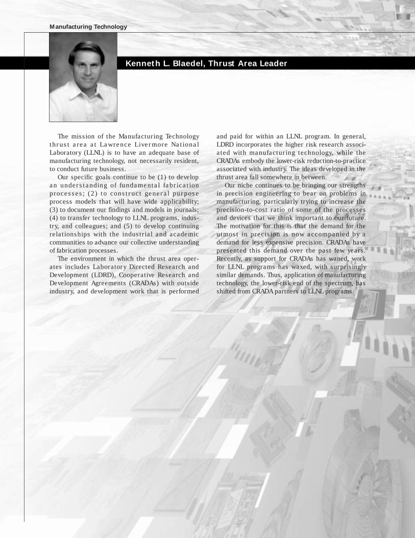
Finally, the third method is to physically bond afine diamond-impregnated wire to the leading edgeof the blade. Typical wire saws for the silicon wafersaw industry use a loose abrasive process.However, for other applications, Laser TechnologyInc. produces a fixed abrasive wire. Figure 2 showsa 250-µm wire with 15-µm diamond abrasive thatwas laser-brazed to the leading edge of a 100-µmstainless steel band. Cutting and durability tests arecontinuing on this sample, but it seems to be aviable option for a prototype saw blade to test, forinstance, the effect of diamond grit size on perfor-mance. The chemically-bonded process is preferredfor production blades.
Conceptual Machine Design
Attempting the design of a production precisionsaw at this early stage of the project forces design-ers and engineers to consider the entire problem ofslicing crystalline materials, not allowing a narrowfocus on only a few aspects. Additionally, a concep-tual machine design has use in describing variousaspects of the project to industrial contacts. Thefollowing list of machine design requirements andfeatures have been identified.
1) Boule and wafer fixturing. Due to the potentialfor large forces being generated by thehydrodynamic blade bearing, the wafer must besubstantially supported to prevent fracture. Ifthis fixturing for the boule and wafer can be astructurally stiff loop that also contains a guidefor the blade entering and exiting the boule, thewafer thickness variation and flatness can beimproved. This fixturing must also allow theboule to be oriented so that cuts are made in theproper relation to the crystallographic plane.
2) Axis configuration. Traditional bandsaws havethe blade wheels rotating about horizontal axesand the part translating on a linear horizontalaxis. Our current thinking maintains thisapproach but uses four wheels and slices on theblade span between the bottom two wheels;hence the symmetry axis of the boule is nowvertical, and parts may be removed from thebottom of the saw.
3) Immersed cutting. To maintain a constantwater supply to the hydrodynamic blade bear-ing, it is preferable to immerse the cuttingregion in a bath of cutting fluid. Of course, aconsideration is the frictional loss due to theviscous fluid action on the rotating wheels.
4) Productivity. For a silicon slicing application,the saw must have high throughput to matchcompetitive technologies. The productivity of
Engineering Research Development and Technology4-2
Figure 2. Diamond-impregnated wire brazed to a stainlesssteel substrate (100×).
Manufacturing Technology
the current machine design will likely comefrom its improved performance, obviating theneed for secondary finishing steps. The currentindustry solution for 300-mm silicon wafers isthe diamond slurry wire saw which appears tobe capable of producing 300 to 3000 wafers/day(12 to 120 wafers/h). It appears likely that aprecision saw can be designed to cut multiple(5 to 10) boules simultaneously, so that athroughput of 60 wafers/h is possible.
5) Cutting force support. A current unknown ishow much force is generated in the in-feeddirection during cutting. This force must beresisted to keep the blade on the wheels. Thedesired solution is to use actively controlledmagnets and a magnetic blade material tomaintain blade position.
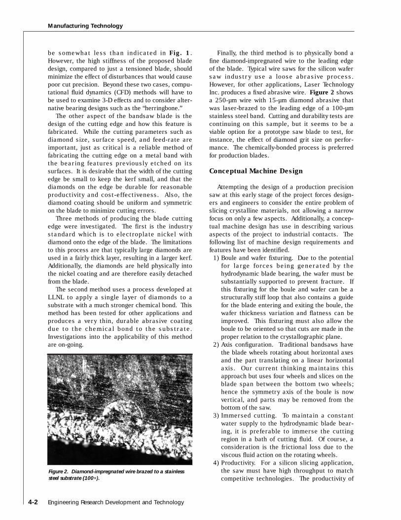
A simplified view of the proposed machine designincorporating these ideas is shown in Fig. 3.
Future Work
The most critical task to pursue in the future is totest the hydrodynamic and cutting characteristics ofthe blade. The current plan begins with blade test-ing in a guide with the hydrodynamic features inreplaceable guides and mechanical wheel bearings.The next steps would be to incorporate the desiredfeatures into the blade with a photo-etching processand to design and fabricate hydrostatic bearings forthe blade wheels. Finally, a cutting blade would betested on a machine with a linear axis to translatethe boule.
Modeling of the hydrodynamic features shouldcontinue with a CFD code to perform detailed designon both simple bearing configurations, such as theparallel and inclined step, and more advancedconcepts such as a herringbone design. A concep-tual machine design should also be developed toexamine critical aspects of a production machineso that necessary concepts can be tested on aprototype machine.
References
1. Hamrock, B. J. (1994), Fluid Film Lubrication,McGraw Hill Co., New York, N.Y.
Thrust Area Report FY 96 4-3
Figure 3. Simplified view of a conceptual production precisionsaw.


Manufacturing Technology
Introduction
One of the strengths of LLNL in the precisionmanufacturing field is its diamond turning capability.Rotationally symmetric workpieces can be machinedto tolerances of just a few microinches. However,one of the severe limitations of this technology isthat only a select few non-ferrous metals (includingcopper, gold, aluminum, and nickel) can bemachined with surface roughness less than 5 nmwith a single-crystal diamond tool. The high qualityworkpiece surface results from the very sharp initialedge of the single-crystal diamond, and the resistanceof the diamond edge to wear against these metals.In contrast, carbide-forming metals such as steel,titanium, and beryllium cannot be similarlymachined, because they cause excessive chemically-induced wear of the diamond.
There is great demand for precision turning ofworkpieces made from carbide-forming metals.Within LLNL, for example, precision components ofsteel and beryllium are of great interest. Within thecommercial sector, the steel bearing process wouldbenefit economically if bearings could be turnedinstead of ground. Within the Department of Defense,there are many current and future components whichwould benefit from high precision turning, such asmirrors machined directly from silicon.
Boron-based coatings are also of interest for otherapplications, including electronics, optical filters,wear-resistance, and high-hardness applications.
Our goal for this project is to turn high-precision,very smooth surfaces on carbide-forming materials,particularly steel, through the use of a hard-coatedtool. This goal is distinguished from many otherhard-coated tool efforts that are directed not at thefinishing stage, but rather at the intermediate orroughing stage of manufacture. In this finishingdomain, a coating thickness of perhaps 1 µm isconsidered a thick coating, and a tool edge radius of1 µm is considered dull. The reward for success isthat the large investment we already have in theinfrastructure to perform diamond turning could bebrought to bear on other desirable materials with asmall incremental cost of a coated tool.
The most successful method, ion-beam assisteddeposition, has a problem with stress delaminationlimiting the thickness of films. We used two meth-ods to produce BN films. The first, sputtering of aboron target in a nitrogen atmosphere is a continua-tion of last year’s work, and the second, e-beamevaporation of boron while simultaneously bombard-ing the substrate with an energetic, neutral nitrogenbeam, is documented in this report. We will refer tothe latter approach as neutral-beam assisted depo-sition (NBAD). The sputtering work was done in
Thrust Area Report FY 96
eposition of Boron Nitride Films via PVD
4-5
David M. Sanders and Steven FalabellaMaterial Fabrication DivisionMechanical Engineering
Daniel M. MakowieckiMaterials Science and Technology DivisionChemistry and Materials Science
A neutral beam-assisted deposition system that has demonstrated the potential of producing high-quality films at reduced stress was assembled and evaluated in a chamber in the Vacuum ProcessesLaboratory of Lawrence Livermore Laboratory (LLNL). Transparent boron nitride (BN) coatings wereproduced, with some varying crystal structure, as evidenced by absorption differences in FTIR scansof films produced with varying amounts of neutral bombardment. However, no conclusive evidence ofthe cubic phase was noted. The films produced were very adherent to silicon substrates and exhibitedlow residual stress, indicating that this process may be able, with additional optimization, to producetechnologically useful cubic BN films.

Manufacturing Technology
LLNL’s Chemistry and Materials Science Department,while the NBAD work was done in its VacuumProcesses Laboratory.
Progress
A NBAD system that has demonstrated the poten-tial of producing high-quality films at reducedstress1 was assembled and evaluated in a chamberin the Vacuum Processes Laboratory at LLNL. An
Ion Tech 3-cm-diameter ion source and customneutralizer cone was used to focus the neutral nitro-gen onto the substrates held on a radiatively-heatedstage. A Balzers e-beam system was installed in thechamber to evaporate the boron. These two systemswere assembled for the first time in this chamber.Since it took much effort to get to a point of reliableoperation there was insufficient time to optimize thedeposition process.
Transparent BN coatings were produced, withsome varying crystal structure as evidenced byabsorption differences in FTIR scans of filmsproduced with varying amounts of neutral bombard-ment. However, no conclusive evidence of the cubicphase was noted. The films produced were veryadherent to silicon substrates and exhibited lowresidual stress, indicating that this process may beable, with additional optimization, to produce tech-nologically useful cubic BN films.
Description of Process
The formation of cubic BN (c:BN) has been shownto require three conditions: a source of boron, asource of energetic nitrogen, and a substratetemperature in the range of 400 to 800 °C. Aphotograph of the system is shown in Fig. 1. ABalzers e-beam evaporator was used as the sourceof boron. The evaporation rate was monitored andcontrolled by an Inficon IC6000 controller andquartz crystal monitor placed near the substrate.The evaporation rate was varied in the 0.5 to 2.0 Å/srange for this series of experiments.
The energetic nitrogen was supplied as a neutralbeam. This beam was produced by directing an ionbeam onto the inside of a cone. An Ion Tech 3-cm,gridded ion source was used, with hollow cathode
Engineering Research Development and Technology4-6
Ab
sorp
tio
n
Ab
sorp
tio
n
-0.25
-0.15
-0.05
0.05
0.15
0.25
3
2
1
0
Wavenumber (cm-1)
800120016002000 800120016002000
(a) (b)
1398.73
1153.71
1391.01
806.44
Figure 1: Photograph of apparatus used for NBAD of BN films.
Figure 2. (a) FTIR scan of typical BN film produced by NBAD system. The absorption near 1390 cm-1 is indicative of the hexagonalphase. (b) FTIR scan of an area that shows absorption near 1150 cm−1, which is evidence of sp3 bonding.

Manufacturing Technology
plasma source using a 50/50 nitrogen/argon gasmix. Inside the outer cone, there was a smaller,inverted cone to block all line of sight to thesubstrate. The cone provides surface neutralizationof the ion beam, while the particle energy is reducedonly slightly due to the glancing angles the ion beammakes with the cones. The ion energy was variedfrom 300 to 550 eV and ion currents from 25 to50 mA over the course of these experiments.
The 2-in. silicon wafers used as substrates wereheld at the exit of the neutralizer cone, in the evapo-ration plume of the boron source, on a heated stage.The temperature of the stage was varied from 400 to550 °C for this series of experiments. The stage hasthe capability of biasing with either rf or dc, but thiswas not used for this work, as the goal was to useneutral nitrogen bombardment of the substrate.
Results
As noted above, transparent BN films wereproduced using the above equipment over a fairlywide range of conditions, but in the limited timeavailable, conditions that produce the cubic phasewere not found. The crystal structure of the filmswas determined using the absorption characteristicsmeasured using FTIR spectrometry in the 700 to2000 cm−1 range. A representative scan is shown inFig. 2a. Most of the films demonstrated a large,broad absorption at 1390 cm−1 and smaller peaknear 800 cm−1, indicative of sp2 (hexagonal) bondedBN. As shown in Fig. 2b, one sample exhibited
absorption at 1150 cm−1, which is close to the cubicphase signature of 1060 cm−1, but we feel that theshift is too great to be explained by intrinsic stress,and may be due to a wurtzite phase.2 Although it issp3 bonded, this phase is metastable and not thehard, cubic phase useful in tool bit coatings.
Conclusions
Although not demonstrated using NBAD, therewere indications that the system could produce c:BNfilms of good adherence and low enough stress tomake coatings thick enough for tool bit use.
Acknowledgments
We wish to thank R. Sanborn of AnalyticalSciences Division for producing the FTIR scans ofour films, and S. Bryan of MMED for assembling andtroubleshooting the Balzers e-beam system.
References
1. Lu, M, A. Bousetta, R. Sukach, A. Bensaoula, K.Walters, K. Eiperssmith, and A. Schultz (1994),“Growth Of Cubic Boron Nitride On Si(100) ByNeutralized Nitrogen Ion Bombardment,” AppliedPhysics Letters, Vol. 64, (12), pp. 1514−1516.
2. Mirkarimi, P. B., K. F. McCarty, and D. L. Medlin,“Critical Review of Advances in Cubic Boron Nitride,”to be published in Science & Technology of HardCoatings, Sundgren and Barnett, Editors.
Thrust Area Report FY 96 4-7


Manufacturing Technology
Introduction
KEM is a low-bulk temperature coating process notrequiring the introduction of thermal energy. Bondingenergy is induced by high-speed impact of fine metalparticles on a substrate. KEM is different from theconventional thermal spray coating processes inwhich the metal particles are heated to the liquidstate and sprayed by a moderate- to high-speedcarrier gas at the substrate to produce coatings. Theprocesses are high-temperature operations. KEM istherefore very attractive for near net shape products.
ITI (Las Cruces, NM) was the first company in theU. S. to produce thin coating deposition samplesthrough KEM technology and has applied for the patentrights. A group of Russian researchers have publishedsimilar work1 called “cold gas-dynamic deposition.”
Our objectives are to demonstrate the technicalfeasibility of the KEM process through a parametricexperimental study in a controlled environment andto establish better understanding of the particle-to-substrate interaction mechanisms. The coating andforming experiments based on a mutually agreedupon test matrix were performed by ITI under acontract with Lawrence Livermore NationalLaboratory (LLNL).
ITI produced a set of thin coatings, on the orderof 10’s of mils, from which process parameters wereselected to generate three bulk (thick) samples, Ti,Cu, and Zn, for further testing and analyses at LLNL.
Preliminary finite element analyses of the impactprocess were carried out at LLNL. The goal of theanalytical studies is to determine the effects of particlevelocity, size, material, and substrate material.
Thrust Area Report FY 96
anufacturing and Coating by Kinetic Energy Metallization
4-9
T. S. ChowDefense Technologies Engineering DivisionMechanical Engineering
We have performed systematic laboratory experiments and modeling analyses to demonstrate that(1) it is feasible to form thin and thick deposits by kinetic energy metallization (KEM) using variousmetal powders onto several types of substrates; (2) very low as-deposited porosity can be achievedby using fine (<10 µm) to ultra fine (<3 µm) powders; (3) KEM deposition rates are favorable forthick buildup for practical applications; and (4) the thick deposits will require post-KEM processesfor improvement in both density and tensile properties. In addition, computer modeling predicts thatthe magnitude of the impact velocity is an important factor and that high deformations are producedin both impacting particles and target materials after impact. Features in the micrographs areconsistent with these predictions.
Gassupply
Gassupply
∆ p = 20 psi
Carrier p Powderfeeder
Recoverysystem
Applicationnozzle
Substrate
Figure 1. Schematicrepresentation of theKEM system.

Manufacturing Technology
Progress
KEM Test System and Process Description
A schematic of the KEM system is shown inFig. 1. The system consists of a supersonic nozzle
for driving µm-sized particles to speeds in excess of300 m/s and a recovery hood for the over-sprayedpowder. The gas source used two K-bottles ofcommercial grade He, regulated to nozzle inlet pres-sures of 500 psig or less. The fluidizing gas pres-sure driving the feeder was regulated to a ∆p of 20
Engineering Research Development and Technology4-10
Table 1. KEM test matrix based on six parameters.
Parameters Lower bound Upper bound Increment Bulk samples
1 Substrate hardness Al Cu or Inconel-600 Al
2 Powder type: Al Cureactivity Cu Timelting point Ni Znhardness Ti
Zn
3 Powder size <3 µm <45 µm 3 sizes <10 µm, 45 (Ti)
4 Gas type N He 2 gases He
5 Nozzle inlet pressure 200 psig 450 psig 3 settings 200 to 300
6 Deposition duration 5 s 60 s 3 values up to 60 s
Table 2. Summary of all runs using Al substrate.
Avg. deposition He gas Hardness Base metalPowder rate (µm/cm2-s) (psig) Porosity RH, 15T RH
Al (<10 µm) 13 ± 7 200 <5% 71 ± 2 77 ± 2Al (<10 µm) 6 ± 5 450 <5% 72 ± 2Al (20 µm), sph 99 ± 20 200 5 to 10% 61 ± 4Al (20 µm), sph 384 ± 20 450 5 to 10% 64 ± 3
Cu (<10 µm) 8 ± 3 100 <5% 77 ± 3 76 ± 1Cu (<10 µm) 84 ± 17 200 5.6 ± 4.5 85 ± 2Cu (<10 µm) 122 ± 23 450 <5% 89 ± 2Cu (<45 µm) 20 ± 1 200 > 10% 76 ± 2Cu (<45 µm) 59 ± 6 450 > 10% 78 ± 3
Ni (<3 µm) 14 ± 5 200 – 88 ± 2 87 ± 1Ni (<3 µm) 23 ± 12 450 – 87 ± 2 (Inconel–600)Ni (<10 µm) 13 ± 4 200 5 to 10% 88 ± 4Ni (<10 µm) 44 ± 7 450 – 92 ± 1
Ti (<45 µm) 29 ± 7 200 18 ± 4.5 78 ± 3 80 ± 1Ti (<45 µm) 42 ± 13 450 > 10% 83 ± 6
Zn (<10 µm) 82 ± 8 to 160 ± 44 200 to 450 <5% 63 ± 4Zn (10 to 25 µm) 15 ± 6 to 20 ± 3 200 to 450 <5% 58 ± 4

Manufacturing Technology
to 30 psig above the process line. Nitrogen gas wasperiodically tested throughout the parametric studyto determine if the KEM depositions were feasiblewith a lower expansion velocity gas.
The test matrix consists of the following parame-ters with a wide range of values: powder materials,powder sizes (commercial grades), carrier gases,pressures, and substrate materials based on hard-ness and deposition thickness (thin film and bulksamples, as summarized in Table 1).
Results
The detailed experimental data and results aregiven in ITI’s final report.2
Table 2 summarizes the results for deposit onaluminum substrates, showing the effects of powdersize, shape and gas pressure on the deposition rate,porosity, and hardness. The large uncertaintiesassociated with the deposition rates were attributedto powder flow rate variations that were highlydependent on the powder properties and the feederbehavior. Generally, higher inlet pressures andsmaller particles tended to increase the depositionrates. A few selected KEM depositions of variouspowders were made on substrates of Cu, Al, and Ni.
The micrographic characterization of all thesamples listed in Table 2 is included in Reference 1.
Micrographic comparison of the particle size effectsare shown in Fig. 2, for Cu (<10 µm) and Cu(<45 µm) on Al. The bulk and interfacial porositieswere quite low (<5%) for the <10-µm Cu, while the<45-µm Cu exhibited moderate porosity (10 to15%). The micrograph of a Cu-on-Cu (Fig. 3)showed a much lower level of interfacial porosity, ascompared to a Cu-on-Al deposit under otherwiseidentical conditions, suggesting that similar metalsform stronger bonding than dissimilar ones.
ITI generated the bulk (thick) samples (Cu, Ti, andZn) on (1mm) Al (Table 3) using the parametersderived from the test matrix. All KEM bulk sampleswere fairly rough on the deposition side because ofmanually operated nozzle translation. The Cu and Tibulk samples exhibited significant residual stressthat resulted in bending of the samples. The Znsample showed much less residual stress.
The post-KEM processes included annealing ofthe Cu sample, and annealing followed by HIP-ing ofthe Ti sample. These treatments greatly improvedthe mechanical properties of the deposits. Table 4is a summary of the analysis and testing results.
Annealing of KEM-deposited Cu had moderatereduction in porosity, (from 6% to 4%), and a slightdecrease in hardness. Annealing and HIP-ing of theKEM-deposited Ti reduced the porosity from 17% to0, and greatly increased the hardness.
Thrust Area Report FY 96 4-11
Figure 2. Micrographs of Cu on Al, <10 µm (a) and <45 µm (b). Figure 3. Micrograph of Cu on Cu.
Table 3. Bulk sample deposition parameters.
Bulk sample Cu Ti Zn
Dimension 8.0 cm × 1.6 cm × 0.6 cm 8.0 cm × 1.7 cm × 0.5 cm 8.0 cm × 1.8 cm × 0.3 cm
Powder size <10 µm <45 µm <10 µm
He pressure 300 psig 250 psig 300 psig
Height of curvature 3.0 mm 2.5 mm 0.5 mm
Radius of curvature 34 32 203

Manufacturing Technology
A tensile specimen (Fig. 4) machined from anannealed Cu sample was tested, with the result plottedin Fig. 5. It can be seen that, with 38 ksi ultimatestress at 0.75% elongation, the specimen was brittlebut relatively strong.
Elemental analysis of the Cu sample shows thatthe bulk oxygen content was in line with the level ofcommercial grade Cu powders. The KEM processfailed to purge out the oxide coating naturally occur-ring on the Cu particle surfaces.
Theoretical Modeling Analysis
There are three major aspects to the KEMphenomenon: (1) the gas dynamics of the super-sonic, gas/solid jet impinging on the target that mayor may not modify the shock waves in front of the
target; (2) the particle impact interaction processesat the surface; and (3) multiple impacts on (thick)KEM samples.
We have concentrated our analytical efforts3,4,5
on the last two problems, that is, the interaction ofthe particle with the solid target upon impact at highvelocities, particularly the time dependent deforma-tion characteristics of both the particles and thesurface on impact. The axi-symmetric 2-D CALEcode that can calculate deformation and movingstress waves in the materials at high strain rateswas used.
We have made calculations for various particle-impact scenarios. Here we discuss several samplecases: Cu particle impact on an Al target at variousvelocities (200 m/s, 500 m/s, and 1,000 m/s); Cuparticle impact on a Cu target at 1 km/s; and two Cu
Engineering Research Development and Technology4-12
Table 4. Bulk samples test summary.
Treatment(1) Rockwell Tensile Machine- Oxygenhardness(2) Density property ability content
Cu As-deposited 87 (15T) 94% — poor 0.209% ± 0.057—Annealed 80 (15T) 96% 38 ksi good comparable to
0.7% general MSDS spec.(ultimate) for Cu powders
Ti As-deposited 82 (15T) 82% — poor —Annealed 32 (C) 93% — poor-fairHIP’ed 38 (C) 100% — fair
Zn As-deposited 74 (15T) 96% — fair —
(1) Annealing condition: 2/3 melting temperature for 3 h; HIP condition: 15 ksi at 1000 °C for 3 h.(2) [15T] is the Rockwell superficial hardness: max. scale = 92.5, equivalent to 19.9 on [C] scale.
(a)
(b)
Figure 4. Annealed KEM-deposited Cu tensile specimen.
40 x 103
35 x 103
30 x 103
25 x 103
20 x 103
15 x 103
10 x 103
5 x 10³
1
Strain (in./in.)
Stre
ss (
psi
)
KEM #1-Cu annealed
1 8 x 10-32 x 10-3 4 x 10⁻³ 6 x 10⁻³
Figure 5. Stress/Strain of annealed KEM-deposited Cu.

Manufacturing Technology
particles impinging on an Al target at 1 km/s. Themodel assumes a moving particle (a cylindricaldisk), about to strike a target at t = 0. Due to axi-symmetry, only the top half of the field is needed inthe simulation.
Case A: Effects of Particle Impact Velocity onParticle/Target Interaction. The deformationpatterns of the Cu and Al materials at t = 0.36 µsafter impact, when the impact velocity was 200 m/s,resulted in only a small amount of deformation.When the impact velocity was increased to 500 m/s,greater deformation took place. The stress waves inthe Al travel first as compressive and then relievingtensile, so that the dilation of the material bringsabout the bulging crater-like protrusions around theimpacting Cu particle.
When the impact velocity is raised to 1,000 m/s,which is a realistic velocity considering the highMach number and velocity for the He carrier gas,our results show marked penetration of the particleas well as fragmentation of the materials. Theseanalytical predictions show indentations and detach-ment of the target materials that resemble thosefound in the ITI test samples.
Case B: Cu Particle Impact on Cu Target. Weconsider this case to determine if there are anydifferences in impact response of like materials.The results at t = 0.24 µs after impact for the defor-mations in both the particle and the target show thatthese deformations are less than those for Cu on Alat t = 0.24 µs after impact at 1,000 m/s, signifyingthat Al deforms more readily than Cu when struck bya Cu particle.
Case C: Two Cu Particles on a Cu Target. Theinitial configuration at t = 0 is that both particles aretraveling toward the target at 1,000 m/s. Att = 0.22 µs after impact, the first particle hasalready struck the target and has proceeded to inter-act with the target, while the second particle is stillmoving toward the target. The interaction shortlyafter the impact of the second particle shows that,at t = 0.24 µs, the penetration of the particles intothe target at the centerline is now even greater and,in addition, the relieving tension waves cause theperipheral region of the target to protrude even more.
The velocity vectors show that the particles arestill moving into the target, which will cause moredeformation in both the target and the impactingparticles at subsequent times.
Summary
This study has demonstrated that it is feasible touse the KEM process to deposit a wide range ofmetal powders to form both thin and thick coatings
on various substrates. The work also has validatedKEM as an efficient method for spraying fine reactiveand pyrophoric powders such as Ti, in an inertgaseous atmosphere without using high-vacuumdeposition technology. Commercially available Tipowder was used.
Post KEM processes such as annealing and/orHIP-ing will greatly improve the mechanical propertiesof the KEM-produced free-standing components.For refurbishment or thin coating applications thepost-processes may not be as important.
The effect of the measured residual oxide on theKEM material property is not well understood. Butit does suggest that powder conditioning and/or in-situ generation of powder as an integral part of theKEM process should be studied.
We have done preliminary modeling analyses ofthe KEM phenomenon. The results indicate thatimpacts by solid particles at high velocities couldcause deformations on both the incident particlesand the target, and that the deformation in the lattermaterial is qualitatively similar to that seen in thetest samples.
Future Work
Our plans are to investigate the KEM processthrough experiments and modeling analyses to ulti-mately produce the optimum process conditions.The proposed tasks are:
1) conducting particle/target interaction experi-ments using a well-instrumented set-up, such asmeasuring the particle velocity and responses ofboth it and the target following the impact;
2) setting up a U-deposit facility and conductingU-6Nb experiments at LLNL to demonstrate thefeasibility of the technology as applied to theU-alloy powder;
3) studying the effects of powder synthesis andconditioning on deposition; and
4) performing process modeling analyses. Many important aspects of this complex metal-
deposition phenomenon remain to be addressed,such as the interaction of the particles with eachother and with the target in fully 3-D impact situa-tions; the bonding process at the surface; and thebehavior of the supersonic 2-phase (gas/solid) flowin front of the target and its effect on the shock waveand, especially, on the velocity distributions of theincident particles.
Acknowledgment
The author thanks S. W. Kang, who wrote thesection on theoretical modeling analysis.
Thrust Area Report FY 96 4-13

Manufacturing Technology
References
1. Alkhimov, A. P., V. F. Kosarev, and A. N. Papin (1990),“A Method of Cold Gas-Dynamic Deposition,” SovietPhysics Doklady, 36(12), pp. 1047−1049.
2. Tapphorn, R., and H. Gabel (1996), Final Report—KEM Process Feasibility Study, ITI, Las Cruces,New M.
3. Chow, T. S. (1996), “Manufacturing and Coating byKinetic Energy Metallization (KEM),” Progress Reportfor Manufacturing Thrust Area, Lawrence LivermoreNational Laboratory, Livermore, Calif., March.
4. Chow T. S., and S. W. Kang (1996), PreliminaryEvaluation of KEM for Fabrication, LawrenceLivermore National Laboratory, Livermore, Calif.
5. Tapphorn, R., and H. Gabel (1996), “Kinetic EnergyMetallization Process Feasibility Study—FinalReport,” Proceedings for the 12th General Meeting ofJOWOG31, Livermore, Calif., ITI, Las Cruces, New M.
Engineering Research Development and Technology4-14

agnet Design and Applications
Manufacturing Technology
Introduction
High-energy physics experiments frequentlyrequire large-aperture spectrometer magnets aswell as high-quality bending and focusingmagnets. Their magnetic fields vary widely inuniformity and symmetry and must be predictedvery accurately. The sophisticated 2-D and 3-Dcomputer simulations often must be verified bydirect magnetic field measurements. Fully auto-matic positioning and magnetic field measuringequipment is required.
At present, there is no facility in the United Statesthat has a full-fledged operating magnetic measure-ment laboratory. Without magnetic measuring capa-bilities, projects requiring magnets are relying oncomputer modeling techniques to accurately designthe magnet to desired specifications. To date, noone has verified the accuracy of these models.
Our project looked at validation of the computa-tional model used to design quadrupole focusingmagnets for the B-Factory project at SLAC. Themagnets were designed by the ATEG in ARED.Magnetic field measurement data was thencompared to the predicted model by ATEG staff.Differences in the predicted fields versus themeasured fields were assessed for computer codemodeling accuracy.
This project also looked at a conceptual approachfor mapping large-scale magnets by designing ascheme to map the PHENIX muon magnets. Theapproach can be applied to other large-scale magnets,such as the Compact Muon Solenoid (CMS) at CERNand the Main Injector Neutrino Oscillation Search(MINOS) at Fermi National Laboratory. A conceptualdesign for mapping bending and focusing magnetswas done by adapting a coordinate measuringmachine at LLNL to accurately position a probe armand probe assembly inside a magnet bore.
Progress
Two modified PEP-I insertion quadrupole magnetswill be used on the high-energy ring (HER) in theinteraction region (IR) of the PEP-II asymmetric B-Factory at SLAC, with the name QF5 quadrupoles.The insertion quadrupoles were designed to providean extremely uniform (DB ≤ 10−4) and pure(Bn/B2 ≤ 10−4) quadrupole field.
Two-dimensional field calculations were performedusing POISSON, a code widely used and acceptedwithin the high-energy physics/accelerator commu-nity. Because the magnet geometry required a modelwith very small elements in a large cross-section, thecode was challenged by the large size of the elementcount as well as by the necessity to have the
Thrust Area Report FY 96 4-15
The primary goal of this project is to demonstrate and provide closure for the magnet designprocess used in the physics/accelerator community. The magnet design closure process comparesthe measured field to the design model for a magnet designed by the Accelerator TechnologyEngineering Group (ATEG) for the Stanford Linear Accelerator (SLAC). Revision of modeling tech-niques will be based on this data comparison to more accurately predict future magnet designs. Asecond goal is to produce a conceptual design of both a specific and generic magnetic field mappingdevice. A conceptual design for a specific magnet mapper is demonstrated by the application of anexisting coordinate measuring machine at Lawrence Livermore National Laboratory (LLNL) to map avariety of standard dipole and quadrupole magnets. A conceptual design of a generic magnet mapperapplicable to large scale magnets is demonstrated for the Muon Magnet of the PHENIX Detectorproject at the RHIC accelerator at Brookhaven National Laboratory (BNL).
Thomas M. VercelliApplied Research Engineering DivisionMechanical Engineering

Manufacturing Technology
dimensions of air/iron interfaces on the order ofthe element dimensions. Magnetic measurementswere performed at LLNL using a 161-mm diameterrotating “search” coil.
The measured multipole errors (normalizedharmonics) were the same order of magnitude as theaccuracy limitations of POISSON. Yet, a comparisonbetween the calculated and measured majorsystematic multipoles (n = 6,10) indicates goodagreement. The comparison indicates that POISSONis an excellent tool for magnet design and that thenon-conventional use of single elements in air/ironinterfaces was successful for this application.
A conceptual design of the PHENIX mapper wascreated, along with a parts list and cost estimate offabrication, assembly, and testing. This designconcept uses a combination of laser interferometryand CCD cameras as the tracking and positioningmeasurement system. Linear probe position (z-axis)is accomplished by a linear slide mounted on aboom. A cart carrying the Hall probes is attached tothe linear slide. The boom rotates at one end and isattached to a wall crawler at the opposite end toachieve an x-y position (Fig. 1). The entire systemis controlled by LABVIEW software.
This approach can be applied to other large-scale magnets such as the CMS. The probe-positioning system is specific to the PHENIXmagnet volume, but the positioning concept,tracking, and control system can be genericallyapplied to other magnets.
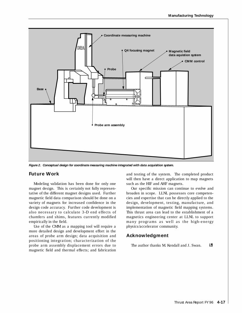
A conceptual design for using a coordinatemeasuring machine (CMM) as a mapping tool wascreated. This design uses the “DEA” CMM as thepositioning device for the magnetic field measure-ment probes. A cantilevered probe arm assemblyis attached to the CMM positioning head. Themagnet to be mapped is placed on top of the gran-ite table of the CMM. The CMM is programmed toposition the field measuring probe inside themagnet bore. A data acquisition system (DAS)records the magnetic field.
The DAS is integrated with the CMM controlsystem, so programmed movements of the measur-ing probe are coordinated with the field mapping.The CMM measures a reference target on themagnet to locate the center and axial location of themagnet bore. Probe position can then beprogrammed for very accurate probe placementduring mapping (Fig. 2).
Engineering Research Development and Technology4-16
4 PSD or CCD cameraswith beamsplitter cells for alignment
Magnet walls
Slider, about 1.3 meter longTwo PSD cells orCCDs and reflectivefoil alignment targets,visible by bothcameras
Wall crawler
Approximately 150reflecting targets aredistributed about the piston ID.
Telescoping extension
4 video cameras for alignment
Center Piston
All cables exit here
4 3-D Hall probesNon-rotating Universal
joint. Boom is flipped here to measure close
to piston.
2 lasers for straightness and roll/yaw
alignment
Air motor drive for linear
slide with optical encoder
Linear slide Rotary drive/gear
The hall probes always face radially outward.To measure the field close to the center piston,the boom is flipped so the hall probes face inward toward the piston.
Figure 1. Conceptual design for PHENIX mapper.
Manufacturing Technology
Future Work
Modeling validation has been done for only onemagnet design. This is certainly not fully represen-tative of the different magnet designs used. Furthermagnetic field data comparison should be done on avariety of magnets for increased confidence in thedesign code accuracy. Further code development isalso necessary to calculate 3-D end effects ofchamfers and shims, features currently modifiedempirically in the field.
Use of the CMM as a mapping tool will require amore detailed design and development effort in theareas of probe arm design; data acquisition andpositioning integration; characterization of theprobe arm assembly displacement errors due tomagnetic field and thermal effects; and fabrication
and testing of the system. The completed productwill then have a direct application to map magnetssuch as the HIF and AHF magnets.
Our specific mission can continue to evolve andbroaden in scope. LLNL possesses core competen-cies and expertise that can be directly applied to thedesign, development, testing, manufacture, andimplementation of magnetic field mapping systems.This thrust area can lead to the establishment of amagnetics engineering center at LLNL to supportmany programs as well as the high-energyphysics/accelerator community.
Acknowledgment
The author thanks M. Kendall and J. Swan.
Thrust Area Report FY 96 4-17
Coordinate measuring machine
Probe
Q4 focusing magnet Magnetic fielddata aquistion system
CMM control
Base
Probe arm assembly
Figure 2. Conceptual design for coordinate measuring machine integrated with data acquisition system.


EnginReseaDeveloand Te
EnginReseaDeveloand Te
THRUST AREA REPORT
Engineering R
esearch, Developm
ent and Technology • FY 96
Thrust Area R
eport • UC
RL 5
38
68
-96
Technical Information DepartmentLawrence Livermore National LaboratoryUniversity of CaliforniaLivermore, California 94551