manual mb86r01 / mb86r02 jade ( d ) evaluation … 5(42) prepared document number manfred ortmann...
TRANSCRIPT

Preliminary1(42)
Prepared Document Number
Manfred OrtmannApproved Checked Date Revision Storage
Manfred Ortmann 20091029 PA 5.6 Mycable01
Receiver: Info:M. CarstensBehrens mycable GmbH
Manual
MB86R01 / MB86R02
JADE ( D ) Evaluation Board
Version PA5.6 October 29, 2009
http://www.fujitsu.com/emea/services/microelectronics

Preliminary2(42)
Prepared Document Number
Manfred OrtmannApproved Checked Date Revision Storage
Manfred Ortmann 20091029 PA 5.6 Mycable01
NoticeThe contents of this document are subject to change without notice. Customers are advised to consult with FUJITSU sales representatives before ordering.
Any information in this document, including functional descriptions and schematic diagrams, shall not be construed as license of the use or the exercising of any intellectual property rights, such as patent rights or copyright or any other right of FUJITSU or any third party or does FUJITSU warrant noninfringement of any thirdparty's intellectual property right or other right by using such information. FUJITSU assumes no liability for any infringement of the intellectual property rights or other rights of third parties which would result from the use of information contained herein.
The products described in this document are designed, developed and manufactured for general use, including unrestricted ordinary industrial use, general office use, personal use, and household use but are not designed, developed and manufactured for use accompanying fatal risks or dangers that, unless extremely high safety levels are ensured, could have a serious effect to the public and could lead directly to death, personal injury, severe physical damage or other loss (i.e., nuclear reaction control in nuclear facility, aircraft flight control, air traffic control, mass transport control, medical life support system, missile launch control in weapon systems), or (2) for use requiring extremely high reliability (i.e., submarine or satellite technology). Please note that FUJITSU will not be liable against you and/or any third party for any claims or damages arising in connection with abovementioned uses of the products.
If any products described in this document represent goods or technologies subject to certain restrictions on export under the Foreign Exchange and Foreign Trade Law of Japan, the prior authorization by the Japanese government will be required for export of those products from Japan.
All rights reserved and Copyright © FUJITSU LIMITED 2009

Preliminary3(42)
Prepared Document Number
Manfred OrtmannApproved Checked Date Revision Storage
Manfred Ortmann 20091029 PA 5.6 Mycable01
Developer’s Manual for JADE Evaluation Board
SummaryThis manual provides detailed technical information for system architects, hardware and software developers, who work with the JADE Evaluation board version PA 2, PA 4 or PA 5 for evaluation and development purpose.
Enclosures
None.
Product Information
This evaluation board was developed to demonstrate the versatile features from the JADE and its interfaces.
The JADE together with DDR SDRAM and Flash memory is implemented as module which is called XXSvideo.
To use further features two extension boards, JADE Evaluation Board Extension Video Input und JADE Evaluation Board Extension Video Output are available which can be plugged on the JADE Evaluation board.

Preliminary4(42)
Prepared Document Number
Manfred OrtmannApproved Checked Date Revision Storage
Manfred Ortmann 20091029 PA 5.6 Mycable01
In addition an evaluation board with fewer features and interfaces is available. It is called XXSterminal.
Now in 2009 an Evaluation Board ( EVB ) JADED is available. It is a module with the JADED, called XXSvideoD like the XXSvideo with the JADE and an EVBJADED interface board. These both boards can be used for this JADE Evaluation board.
Revision History
Revision Date Sign Description
PA4 20070510 mo First edition for review
PA 5 20070703 mo Consider PCB version PA5
PA 5.1 20080409 mo 2.2.7 Ethernet
2.2.13 video outputs
2.2.16 MOST interface
2.2.17 GPIO expander
PA 5.2 20080820 mo 2.2.13 Video Outputs
pinning of X502 ( I2C0 to I2C1 ) corrected
PA 5.3 20090203 mo Description for EVBJADED added
PA 5.4 20090930 mo JTAGSEL config added
PA 5.5 20091006 mo Picture changed
PA 5.6 20091029 mo 1.3 Changes between PCB Revision PA4 and PA5 added
Contact Information
mycable GmbHMichael CarstensBehrens( hardware and commercial )
Email [email protected]
Tel. +49 4321 55956 55
mycable GmbHCarsten SchneiderEmail [email protected]
mycable GmbHManfred OrtmannEmail [email protected]

Preliminary5(42)
Prepared Document Number
Manfred OrtmannApproved Checked Date Revision Storage
Manfred Ortmann 20091029 PA 5.6 Mycable01
Table of Contents1 OVERVIEW....................................................................................................................6
1.1 Manual Scope........................................................................................................61.2 Putting into Operation.............................................................................................61.3 Changes between PCB Revision PA4 and PA5.....................................................6
2 JADE EVALUATION...................................................................................................7
2.1 System Architecture...............................................................................................72.2 Function Units......................................................................................................10
2.2.1 XXSvideo Module or EVBJADED..............................................................112.2.2 Config Switches............................................................................................122.2.3 Overview of Multiplex Function Groups of JADE .......................................142.2.4 Power Supply...............................................................................................152.2.5 Reset...........................................................................................................152.2.6 Serial Ports..................................................................................................162.2.7 Ethernet.......................................................................................................172.2.8 EJTAG.........................................................................................................192.2.9 Trace Interface Connector ..........................................................................202.2.10 Universal Serial Bus ( USB )......................................................................212.2.11 CAN Port...................................................................................................222.2.12 Video Inputs..............................................................................................242.2.13 Video Outputs............................................................................................262.2.14 Buttons......................................................................................................302.2.15 LEDs.........................................................................................................312.2.16 Media Oriented Systems Transport ( MOST ) Interface............................322.2.17 GPIO Expander.........................................................................................332.2.18 Extension..................................................................................................342.2.19 Secure Digital ( SD ) Memory Card Interface............................................38
2.3 Hardware Variants............................................................................................392.4 Placement of Components...............................................................................402.5 Mechanical Dimensions........................................................................................42
Preliminary6(42)
Prepared Document Number
Manfred OrtmannApproved Checked Date Revision Storage
Manfred Ortmann 20091029 PA 5.6 Mycable01
1 Overview
1.1 Manual Scope
This manual provides detailed technical information about the JADE Evaluation board for system architects, hardware and software developers covering:
• System architecture description and users manual
• Hardware architecture
• Operating system independent software drivers
• Operating system specific board support packages
• Mechanical information
• References to further information like design data, data sheets, software documentation
It is the engineer’s reference for evaluation, system development and prototyping based on the module. This document covers all available hardware versions regarding their configuration options and revision state.
1.2 Putting into Operation
Read the manuals from the used board and set the configuration which is corresponding to your application !
Plug the extension board only if the power supply is off !
1.3 Changes between PCB Revision PA4 and PA5
On PCB revision PA4 it was not designed to use the interrupt signals INT_A2 or INT_A3 for the Extension Video Output board which can be connected with RGB digital output 0 connector X502.
On PCB revision PA5 following population options are added:
The interrupt signal INT_A3 is connected over 0 Ohm resistor R531 with X502 pin 3. Alternativ INT_A2 can be connected with X502 pin 3 by population of resistor R530.
If INT_A2 shall be used by the Extension Video Out the interrupt signal line from the MOST controller can be disconnected by removing 0 Ohm resistor R1428.
Additionally INT_A3 can be disconnected by removing 0 Ohm resistor R1712 from the GPIO expander interrupt output.
On PCB revision PA5 the termination of the ethernet line is changed. It is not known whether this anything changes for the function. It is done to consider a application note from the ethernet transceiver. More details see chapter ethernet.

Preliminary7(42)
Prepared Document Number
Manfred OrtmannApproved Checked Date Revision Storage
Manfred Ortmann 20091029 PA 5.6 Mycable01
2 JADE Evaluation
2.1 System Architecture
The system architecture of the JADE Evaluation board is shown in picture 21.
Pic. 21: JADE Evaluation board block diagram

Preliminary8(42)
Prepared Document Number
Manfred OrtmannApproved Checked Date Revision Storage
Manfred Ortmann 20091029 PA 5.6 Mycable01
Picture 22 shows the top side of the JADE Evaluation board with XXSvideo modul and picture 23 shows the bottom side.
Pic. 22: JADE Evaluation board top side

Preliminary9(42)
Prepared Document Number
Manfred OrtmannApproved Checked Date Revision Storage
Manfred Ortmann 20091029 PA 5.6 Mycable01
Pic. 23: JADE Evaluation board bottom side
Preliminary10(42)
Prepared Document Number
Manfred OrtmannApproved Checked Date Revision Storage
Manfred Ortmann 20091029 PA 5.6 Mycable01
2.2 Function UnitsOverview in the available interfaces:
– 10/100 Ethernet
– 2x serial ports
– 2x CAN
– DVII
– PowerSupply
– Video Input
– USB Host
– USB Device
– JTAG Interface
– Video In 1Interface and I2C
– GPIOs and I2CHeaders
– Digital Video Out Connector
– MOST Interface
– Extension Interface
– SD/MMCCard Slot (bottom side)

Preliminary11(42)
Prepared Document Number
Manfred OrtmannApproved Checked Date Revision Storage
Manfred Ortmann 20091029 PA 5.6 Mycable01
2.2.1 XXSvideo Module or EVBJADED
The connectors X701 ( CPU signals side ) and X801 ( IO signals side ) DF17(2.0)120DP0.5V(51) from Hirose are the interfaces to the XXSvideo module with the JADE and memory or to the EVBJADED with the JADED.
Detailed information on the XXSvideo or XXSvideoD module or EVBJADED interface board see the manuals to these boards.
Do not plug the XXSvideo module or EVBJADED when the power supply is on !

Preliminary12(42)
Prepared Document Number
Manfred OrtmannApproved Checked Date Revision Storage
Manfred Ortmann 20091029 PA 5.6 Mycable01
2.2.2 Config Switches
Before power on the dip switches have to be set.Setting ON means the corresponding signal will be connected to GND and becomes logical 0.Else the pull up resistor operates and the corresponding signal becomes logical 1. Switches of the left dip switch SW901 configure functions of the JADE on the XXSvideo modul or JADED on the XXSvideoD modul.Details see JADE or JADED datasheet.
Following table shows the assignment of switches of SW901 and function of JADE only.
Switch Signal Default Function
1 MPX_MODE_5_0 ON See JADE datasheet
2 MPX_MODE_5_1 ON See JADE datasheet
3
USB_MODE ON 0: USB host
1: USB device
4
BIGEND ON 0: Little Endian
1: Big Endian
5 VINITHI ON See JADE datasheet
6
JTAGSEL ON 0: JTAG interface enabled,
1: JTAG interface disabled

Preliminary13(42)
Prepared Document Number
Manfred OrtmannApproved Checked Date Revision Storage
Manfred Ortmann 20091029 PA 5.6 Mycable01
Following table shows the assignment of switches of SW901 and function of JADED only.
Switch Signal Default Function
1 MPX_MODE_1_0 ON See JADED datasheet
2 MPX_MODE_1_1 ON See JADED datasheet
3 USB_MODE ON No function
4
TESTMODE_2 ON 0: Little Endian
1: Big Endian
5 VINITHI ON See JADED datasheet
6
JTAGSEL ON 0: Fujitsu TAP controller,
1: ARM TAP controller
Switches of the right dip switch SW902 configure functions on the JADE Evaluation board.
Following table shows the assignment of switches of SW902 and function.
Switch Signal Default Function
1 CAN_GROUP2_EN# ON
2
CAN_GROUP4_EN# OFF
Set only switch 1 or switch 2 ON,
do NOT set switch 1 and switch 2 ON !
Details see chapter CAN Interfaces
switch 1 0: only if CAN interface is assigned to function group 2
switch 2 0: only if CAN interface is assigned to function group 4
for JADED set CAN_GROUP2_EN# OFF and CAN_GROUP4_EN# ON
3
VIN0_EN# OFF Important and detail information
see chapter Video Inputs
4
VIN1_EN# OFF Important and detail information
see chapter Video Inputs
5
MOST_EN# OFF Details see chapter MOST Interface
0: enable MLB interface lines
1: disable MLB interface lines
6 RESERVED_SW OFF No function

Preliminary14(42)
Prepared Document Number
Manfred OrtmannApproved Checked Date Revision Storage
Manfred Ortmann 20091029 PA 5.6 Mycable01
2.2.3 Overview of Multiplex Function Groups of JADE
Multiplex Function Group 1 Mode 1 and 2 not used
Multiplex Function Group 1 Mode 0
Pin Name Signal In / Out Function
JADE_IO_G1_[23:0] Out RGB video output
Multiplex Function Group 2
Multiplex Function Group 2 Mode 3 and 4
JADE_IO_G2_[21:0] In / Out Extension Video Input
ITU656 Video Input
CODEC
Multiplex Function Group 2 Mode 5, 6 and 7
JADE_IO_G2_[2:0] In / Out MOST MLB
JADE_IO_G2_[12:9] In / Out CAN
PD 2 JADE_IO_G2_16 Out CAN_1_TX_STBY
PD 3 JADE_IO_G2_15 Out CAN_1_TX_EN
PD 4 JADE_IO_G2_8 Out CAN_0_TX_STBY
PD 5 JADE_IO_G2_7 Out CAN_0_TX_EN
Multiplex Function Group 3
Multiplex Function Group 3 Mode 8 and 9
USB Host and device
Multiplex Function Group 4
Multiplex Function Group 4 Mode 10
JADE_IO_G4_[31:0] In / Out Extension Video Input IDE
Multiplex Function Group 4 Mode 11
JADE_IO_G4_[19:16] In / Out CAN
PD 20 JADE_IO_G4_23 Out CAN_1_TX_STBY
PD 21 JADE_IO_G4_22 Out CAN_1_TX_EN
PD 22 JADE_IO_G4_21 Out CAN_0_TX_STBY
PD 23 JADE_IO_G4_20 Out CAN_0_TX_EN

Preliminary15(42)
Prepared Document Number
Manfred OrtmannApproved Checked Date Revision Storage
Manfred Ortmann 20091029 PA 5.6 Mycable01
2.2.4 Power Supply
Connect the JADE Evaluation board with a power supply between 6 and 25 V DC and approximate 10 Watt at connector X101.
Be aware to use the correct polarity as shown in picture 25.
Pic. 25: Polarity of the JADE Evaluation board power supply connector
A protection against wrong polarity ( D101 ) and overcurrent ( F101 ) is implemented but a too high current can damage the power supply or can produce great heat !Do not plug the XXSvideo or XXSvideoD modul or EVBJADED when the power supply is on !
The required voltages will be regulated from switching power regulators on the board, LT1374IFE from Linear Technologies ( U101 ) for +5 V and LTC3412AEFE from Linear Technologies ( U102 ) for +3.3 V.
2.2.5 Reset
A supervisory circuits which monitors the power supply voltage levels and generates a power on reset signal is implemented on the XXSvideo and XXSvideoD module. A manual reset can be triggered with the button SW804 on the JADE Evaluation board.

Preliminary16(42)
Prepared Document Number
Manfred OrtmannApproved Checked Date Revision Storage
Manfred Ortmann 20091029 PA 5.6 Mycable01
2.2.6 Serial Ports
At the 9pin SubD double stack male connector X1301 are two serial ports with RS232 inputs and outputs available, UART0 at the upper connector and UART1 at the lower connector.
As transceiver with enhanced electrostatic discharge ( ESD ) protection the MAX3387E ( U1301 ) is used.
UART0 with 1152008N1 settings is the default bootloaderconsole.

Preliminary17(42)
Prepared Document Number
Manfred OrtmannApproved Checked Date Revision Storage
Manfred Ortmann 20091029 PA 5.6 Mycable01
Following table shows the assignment of pins, signals and function from the UART connector.
Pin Upper
connector
Lower
connector
Function
1 NC NC Not connected
2 RxD RxD Receive data
3 TxD TxD Transmit data
4 NC NC Not connected
5 GND GND Ground
6 NC NC Not connected
7 RTS NC Request to send
8 CTS NC Clear to send
9 NC NC Not connected
2.2.7 Ethernet
At the RJ45 connector X1101 the Ethernet interface is available.The Ethernet interface is implemented with the 10/100 Ethernet controller LAN9218 ( U1101 ) from SMSC. The LAN9218 is connected to the 16Bit processor interface of the JADE or JADED. Interrupt A0 is used.
The LAN9218 is fully IEEE 802.3 10BASET and 802.3u 100BASETX compliant and supports HP AutoMDIX. The LAN9218 includes an integrated Ethernet MAC and PHY, large transmit and receive data FIFOs with a highspeed host bus interface to accommodate high bandwidth and high latency applications.The LAN9218 also supports features which reduce or eliminate packet loss. Its internal 16kByte SRAM can hold over 200 received packets. If the receive FIFO gets too full, the LAN9218 can automatically generate flow control packets to the remote node or assert backpressure on the remote node by generating network collision.

Preliminary18(42)
Prepared Document Number
Manfred OrtmannApproved Checked Date Revision Storage
Manfred Ortmann 20091029 PA 5.6 Mycable01
The default ethernet setting by pin strapping at the SPD_SEL pin of U1101 is speed 100 Mbps, halfduplex and auto negotation enabled because this pin will be strapped to VCC by the 4k7 Ohm resistor R1112.It is possible to strap this pin to ground by a 0 Ohm resistor R1115 then the settings would be speed 10 Mbps, halfduplex and auto negotiation disabled.
As default the FIFO_SEL pin of U400 is strapped by 0 Ohm resistor R1116 to ground.If this resistor is not populated the FIFO_SEL pin is strapped by the 4k7 Ohm resistor R1113 to VCC then all accesses to U1101 are to the RX or TX data FIFO and the upper addresses A[7:3] are ignored.
As default the AMDIX_EN pin of U1101 is strapped by the 4k7 Ohm resistor R1114 to VCC so AutoMDIX is enabled. That means if the user plugs in either a direct connect LAN cable or a crossover patch cable U1101 is capable of configuring the TPO and TPI twisted pair pins for correct transceiver operation. It is possible to strap this pin to ground by a 0 Ohm resistor R1117 then AutoMDIX is disabled.
An application note from Broadcom says that the 50 Ohm termination resistors ( R104 – R107 ) should be connected to power supply.Up to now the termination resistors are connected over capacitors C1117 and C1118 to GND. Problems are not known.On PCB revision PA5 a population option is added. If 0 Ohm resistor R1118 is populated ( default ) the termination resistors are connected to power supply. If the termination resistors shall be connected as up to now R1118 and R1120 must be removed and 0 Ohm resistor R1119 has to be populated.
Preliminary19(42)
Prepared Document Number
Manfred OrtmannApproved Checked Date Revision Storage
Manfred Ortmann 20091029 PA 5.6 Mycable01
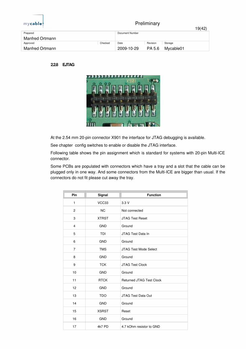
2.2.8 EJTAG
At the 2.54 mm 20pin connector X901 the interface for JTAG debugging is available.
See chapter config switches to enable or disable the JTAG interface.
Following table shows the pin assignment which is standard for systems with 20pin MultiICE connector.
Some PCBs are populated with connectors which have a tray and a slot that the cable can be plugged only in one way. And some connectors from the MultiICE are bigger than usual. If the connectors do not fit please cut away the tray.
Pin Signal Function
1 VCC33 3.3 V
2 NC Not connected
3 XTRST JTAG Test Reset
4 GND Ground
5 TDI JTAG Test Data In
6 GND Ground
7 TMS JTAG Test Mode Select
8 GND Ground
9 TCK JTAG Test Clock
10 GND Ground
11 RTCK Returned JTAG Test Clock
12 GND Ground
13 TDO JTAG Test Data Out
14 GND Ground
15 XSRST Reset
16 GND Ground
17 4k7 PD 4.7 kOhm resistor to GND

Preliminary20(42)
Prepared Document Number
Manfred OrtmannApproved Checked Date Revision Storage
Manfred Ortmann 20091029 PA 5.6 Mycable01
Pin Signal Function
18 GND Ground
19 4k7 PD 4.7 kOhm resistor to GND
20 GND Ground
2.2.9 Trace Interface Connector
At the 10pin connector X902 the Trace interface from the JADE is available.
The trace signals are in function group 5 mode 12. For details see JADE datasheet.
Following table shows the assignment of pins and signals.
Pin Signal Function
1 JADE_IO_G5_0 TRACECLK
2 GND Ground
3 JADE_IO_G5_1 TRACECTL
4 JADE_IO_G5_5 TRACEDATA_0
5 JADE_IO_G5_2 TRACEDATA_3
6 NC Not connected
7 JADE_IO_G5_3 TRACEDATA_2
8 NC Not connected
9 JADE_IO_G5_4 TRACEDATA_1
10 NC Not connected

Preliminary21(42)
Prepared Document Number
Manfred OrtmannApproved Checked Date Revision Storage
Manfred Ortmann 20091029 PA 5.6 Mycable01
2.2.10 Universal Serial Bus ( USB )
The power supply for USB devices which will connected to the JADE Evaluation USB2.0 interface will be controlled from power distribution switch TPS2031D ( U1601 ) from Texas Instruments.This devices is a 50m Ω Nchannel MOSFET highside power switch. The switch is controlled by a logic enable ( EN ).The logic enable disables the power switch, the bias for the charge pump, driver and other circuitry to reduce the supply current to less than 10 µA when a logic low is present on EN . A logic high input on EN restores bias to the drive and control circuits and turns the power on. When the output load exceeds the currentlimit threshold 0.9 A or a short is present, the TPS2031D limits the output current to a safe level by switching into a constantcurrent mode, pulling the overcurrent ( OC# ) logic output low.When continuous heavy overloads and short circuits increase the power dissipation in the switch, causing the junction temperature to rise, a thermal protection circuit shuts off the switch to prevent damage. Recovery from a thermal shutdown is automatic once the device has cooled sufficiently. Internal circuitry ensures the switch remains off until valid input voltage is present.The OC open drain output is asserted active low when an overcurrent or overtemperature condition is encountered. The output will remain asserted until the overcurrent or overtemperature condition is removed.The OC status can be read from the GPIO GPB4.
Following table shows the assignment of power distribution switch pin, signal and GPIO:
Switch Pin Signal GPIO
OC# USB_OVER_CURRENT GPB4
A single transient voltage suppressor SN65220 ( U1602 ) is designed to provide electrical noise transient protection to the USB port but the capacitance of this device makes itunsuitable for USB2.0 and is not populated.
Be aware that this interface does not work because there is a bug in the JADE !The JADED do not have an USB interface. For USB a USB host and device controller is used on the EVBJADED interface board.

Preliminary22(42)
Prepared Document Number
Manfred OrtmannApproved Checked Date Revision Storage
Manfred Ortmann 20091029 PA 5.6 Mycable01
For details see manual of the EVBJADED interface board.Perhaps R1601, R1602 and R1603 have to be removed.This has to be tested.
2.2.11 CAN Port
At the 9pin SubD female connector X1001 are two CAN interfaces CAN0 and CAN1 available.
The CAN transceiver SN65HVD234D from Texas Instruments ( U1002 and U1004 ) provides transmit and receive capability between the differential CAN bus and the JADE with its implemented CAN controllers.
The RS pin 8 of the SN65HVD234 provides for three modes of operation: highspeed,slope control or lowpower standby mode. The highspeed mode of operation is selected by connecting pin 8 directly to ground, allowing the driver output transistors to switch on and off as fast as possible with no limitation on the rise and fall slope. The rise and fall slope can be adjusted by connecting a resistor to ground at pin 8, since the slope is proportional to the pin’s output current. Slope control is implemented with a resistor value of 10 k to achieve a slew rate of 15 V/us and a value of 100 k to achieve 2.0 V/s slew rate. The SN65HVD234 enter a lowcurrent standby mode during which the driver is switched off and the receiver remains active if a high logic level is applied to pin 8. The local protocol controller reverses this lowcurrent standby mode when it needs to transmit to the bus.
The SN65HVD234 enters an ultralowcurrent sleep mode in which both the driver and receiver circuits are deactivated if a low logic level is applied to EN pin 5. The device remains in this sleep mode until the circuit is reactivated by applying a high logic level to pin 5.

Preliminary23(42)
Prepared Document Number
Manfred OrtmannApproved Checked Date Revision Storage
Manfred Ortmann 20091029 PA 5.6 Mycable01
Following table shows the assignment of transceiver pin, signals and GPIOs.The GPIOs belonged to function group 2 in mode 5, 6 or 7.
Transceiver Pin Signal GPIO
CAN_0_TX_EN JADE_IO_G2_7 PD 5
CAN_0_TX_STBY JADE_IO_G2_8 PD4
CAN_1_TX_EN JADE_IO_G2_3 PD18
CAN_1_TX_STBY JADE_IO_G2_2 PD17
Following table shows the assignment of transceiver pin, signals and GPIOs.The GPIOs belonged to function group 4 in mode 11.
Transceiver Pin Signal GPIO
CAN_0_TX_EN JADE_IO_G4_20 PD 23
CAN_0_TX_STBY JADE_IO_G4_21 PD22
CAN_1_TX_EN JADE_IO_G4_22 PD21
CAN_1_TX_STBY JADE_IO_G4_23 PD20
120 Ohm termination is configurable per line via switches on board:SW1001: 120 Ohm Termination for CAN 0SW1002: 120 Ohm Termination for CAN 1
ConnectorType: SUBD 9Pin Female on board
Pin Name Function
1 VCC33 3,3V switchable via R1003
2 CAN_0_L CAN 0 Low
3 GND Ground
4 CAN_1_L CAN 1 Low
5 GND Ground
6 GND Ground
7 CAN_0_H CAN 0 High
8 CAN_1_H CAN 1 High
9 VCC50 5V swichable via R1002
If the JADED is used only one configuration option is possible. See configuration switches.

Preliminary24(42)
Prepared Document Number
Manfred OrtmannApproved Checked Date Revision Storage
Manfred Ortmann 20091029 PA 5.6 Mycable01
2.2.12 Video Inputs
Two 9pin mini DIN connectors X201 and X301 for colour video baseband signals ( CVBS ), 4 CVBS or 2 Y/C or 1 Y/C and 2 CVBS, are available. Each connector is connected to a 9bit video input processor SAA7113H ( U201 and U301 ) from Philips Semiconductors which decoded the analog video signal to a digital video signal with ITU 656 format.Connector X201 is connected to U201. Connector X301 is connected to U301.
Following picture shows the pin assignment of X201 and X301.

Preliminary25(42)
Prepared Document Number
Manfred OrtmannApproved Checked Date Revision Storage
Manfred Ortmann 20091029 PA 5.6 Mycable01
The digital video signal outputs of SAA7113H U201 are buffered with tristate buffers U401and U402 and connected to the video capture interface 0 from the JADE. The buffers are active only if config switch 3 of SW902 ( see chapter Config Switches ) is ON.The video capture interface 0 is connected to connector X401( FTSH10601LDV from Samtec ) also. X401 is foreseen for an external source with a digital video signal with ITU 656 format.
ImportantIf an external video source is connected config switch 3 of SW902 must be set OFF else the outputs from the buffers U401 and U402 and the outputs from the external source work again each other and could be damaged. The digital video signal outputs of SAA7113H U301 are buffered with tristate buffers U402 and U403 and connected to the video capture interface 1 in multiplex function group 2 mode 3 from the JADE. The buffers are active only if config switch 4 of SW902 ( see chapter Config Switches ) is ON.
ImportantIf the digital video signal outputs of SAA7113H U301 shall not be captured set config switch 4 of SW902 OFF else the outputs from the buffers U402 and U403 and other outputs work again each other and could be damaged.
The SAA7113H will be controlled by I2C interface 0.
The RTS0 pin from SAA7113H U201 is strapped to ground so the slave address for readings is 0x49 and the slave address for writings is 0x48.
The RTS0 pin from SAA7113H U301 is strapped to VCC33 so the slave address for readings is 0x4B and the slave address for writings is 0x4A.
Following table show the assignment from pins of X401 and signals:
Pin Signal Function
1 VIN1_0
2 VIN1_1
3 VIN1_2
4 VIN1_3
5 VIN1_4
6 VIN1_5
7 VIN1_6
8 VIN1_7
9 I2C_SCL1 SCL from I2C interface 1
10 I2C_SDA1 SCL from I2C interface 1
11 GND Ground
12 GND Ground
The I2C interface 1 at X401 is foreseen to control external devices.

Preliminary26(42)
Prepared Document Number
Manfred OrtmannApproved Checked Date Revision Storage
Manfred Ortmann 20091029 PA 5.6 Mycable01
2.2.13 Video Outputs
The following description of the video outputs is relevant if a XXSvideo module is used.If a EVBJADED is used see manual of this board.
The digital RGB666 video output 0 from the JADE are connected to connector X502 ( FW2005FD450150A from Samtec ). This connector is higher than connector X602 because this connector is assigned for the JADE Extension Board Video Output.
Only on prototypes the connector X502 is not higher than X602.
The digital RGB666 video output 1 from the JADE are connected to connector X602 ( FTSH12001LDVEJP from Samtec ).
X502 and X602 mate with Samtec types FFSD , CLP , FLE , SFMC , SFMH , TFMDL.
Following table show the pin assignment of connector X502:
Pin Signal Function
1 GND Ground
2 GND Ground
3VO0_B0 Revision PA4: Reserved for Digital RGB output 0
Data blue
( INT_A2 ) / INT_A3 Revision PA5: Interrupt from Extension
4 VO0_B1 Reserved for Digital RGB output 1 Data blue

Preliminary27(42)
Prepared Document Number
Manfred OrtmannApproved Checked Date Revision Storage
Manfred Ortmann 20091029 PA 5.6 Mycable01
Pin Signal Function
5 VO0_B2 Digital RGB output 2 Data blue
6 VO0_B3 Digital RGB output 3 Data blue
7 VO0_B4 Digital RGB output 4 Data blue
8 VO0_B5 Digital RGB output 5 Data blue
9 VO0_B6 Digital RGB output 6 Data blue
10 VO0_B7 Digital RGB output 7 Data blue
11 VO0_G0 Reserved for Digital RGB output 0 Data green
12 VO0_G1 Reserved for Digital RGB output 1 Data green
13 VO0_G2 Digital RGB output 2 Data green
14 VO0_G3 Digital RGB output 3 Data green
15 VO0_G4 Digital RGB output 4 Data green
16 VO0_G5 Digital RGB output 5 Data green
17 VO0_G6 Digital RGB output 6 Data green
18 VO0_G7 Digital RGB output 7 Data green
19 VCC33 + 3.3 V power supply
20 VCC33 + 3.3 V power supply
21 VCC33 + 3.3 V power supply
22 VCC33 + 3.3 V power supply
23 VO0_R0 Reserved for Digital RGB output 0 Data red
24 VO0_R1 Reserved for Digital RGB output 1 Data red
25 VO0_R2 Digital RGB output 2 Data red
26 VO0_R3 Digital RGB output 3 Data red
27 VO0_R4 Digital RGB output 4 Data red
28 VO0_R5 Digital RGB output 5 Data red
29 VO0_R6 Digital RGB output 6 Data red
30 VO0_R7 Digital RGB output 7 Data red
31 HSYNC0 Video output interface horizontal sync output
32 VSYNC0 Video output interface vertical sync output
33 DE0 DE / CSYNC
34 NC Not connected
35 GV0 Video output interface graphics / video switch
36 VO0_CLK_RGBD Video output interface dot clock output
37 I2C_SCL1 I2C interface 1 SCL
38 I2C_SDA1 I2C interface 1 SDA

Preliminary28(42)
Prepared Document Number
Manfred OrtmannApproved Checked Date Revision Storage
Manfred Ortmann 20091029 PA 5.6 Mycable01
Pin Signal Function
39 GND Ground
40 GND Ground
Up to PCB revision PA 4 the pin 3 of connector X502 is not connected.
In PCB revision PA 5 the pin is connected to INT_A3 if the 0 Ohm resistor R531 ispopulated ( default population ).
If the 0 Ohm resistor R530 will be populated the pin is connected to INT_A2. R531 should be removed.
The interrupt pin of the I/O expander U1701 is connected to INT_A3. But on revision PA5 this interrupt can be disconnected by removing R1712.
The interrupt pin of the MOST controller U1402 is connected to INT_A2. But on revision PA5 this interrupt can be disconnected by removing R1428.
The interrupt is foreseen for the interrupt of the touch panel controller on the extension video out.
Following table show the pin assignment of connector X602:
Pin Signal Function
1 VCC50 + 5.0 power supply
2 VCC50 + 5.0 power supply
3 PWMO1 PWMO1
4 GND Ground
5 GND Ground
6 VCC33 + 3.3 power supply
7 VCC33 + 3.3 power supply
8 TFT_MODE Default hi ( R630,R633 )
9 DE1 DE / CSYNC
10 VSYNC1 Video output interface vertical sync output
11 HSYNC1 Video output interface horizontal sync output
12 GND Ground
13 VO1_B7 Digital RGB output 7 Data blue
14 VO1_B6 Digital RGB output 6 Data blue
15 VO1_B5 Digital RGB output 5 Data blue
16 GND Ground
17 VO1_B4 Digital RGB output 4 Data blue

Preliminary29(42)
Prepared Document Number
Manfred OrtmannApproved Checked Date Revision Storage
Manfred Ortmann 20091029 PA 5.6 Mycable01
Pin Signal Function
18 VO1_B3 Digital RGB output 3 Data blue
19 VO1_B2 Digital RGB output 2 Data blue
20 GND Ground
21 VO1_G7 Digital RGB output 7 Data green
22 VO1_G6 Digital RGB output 6 Data green
23 VO1_G5 Digital RGB output 5 Data green
24 GND Ground
25 VO1_G4 Digital RGB output 4 Data green
26 VO1_G3 Digital RGB output 3 Data green
27 VO1_G2 Digital RGB output 2 Data green
28 GND Ground
29 VO1_R7 Digital RGB output 7 Data red
30 VO1_R6 Digital RGB output 6 Data red
31 VO1_R5 Digital RGB output 5 Data red
32 GND Ground
33 VO1_R4 Digital RGB output 4 Data red
34 VO1_R3 Digital RGB output 3 Data red
35 VO1_R2 Digital RGB output 2 Data red
36 GND Ground
37 VO1_CLK_RGBD Video output interface dot clock output
38 GND Ground
39 TFT_LR Default hi ( R632,R635 )
40 TFT_UD Default lo ( R631,R634 )
The transmitter SiI164CT64 ( U501 and U601 ) from Silicon Image uses PanelLink® Digital technology to support displays ranging from VGA to UXGA resolutions ( 25 – 165 Mpps ) in a single link interface. The link interface of U501 is connected to DVII connector X501. The link interface of U601 is connected to DVI connector X601.The SiI164 transmitter has a highly flexible interface with either a 12bit mode ( ½ pixel per clock edge ) or 24bit mode 1pixel / clock input for true color ( 16.7 million ) support. In 24bit mode, the SiI164 supports single or dual edge clocking. In 12bit mode, the SiI164 supports dual edge single clocking or single edge dual clocking.The SiI164 can be programmed though the I2C interface 0. The multifunction address inputs A1, A2 and A3 of U501 are strapped to ground so the slave address for readings is 0x71 and the slave address for writings is 0x70. The multifunction address inputs of U501 A2 and A3 are strapped to ground and A1 is strapped to VCC so the slave address for readings is 0x73 and the slave address for writings is 0x72. The SiI164 support receiver and hot plug detection.
Preliminary30(42)
Prepared Document Number
Manfred OrtmannApproved Checked Date Revision Storage
Manfred Ortmann 20091029 PA 5.6 Mycable01
The triple 8Bit high speed video digitaltoanalog converter ( DAC ) ADV7125JSTZ240 ( U502 and U602 ) from Analog Devices convert the digital RGB666 video output signals from the JADE to an analog video signals. Outputs from U502 are connected to DVII connector X501. Outputs from U602 are connected to DVII connector X601.
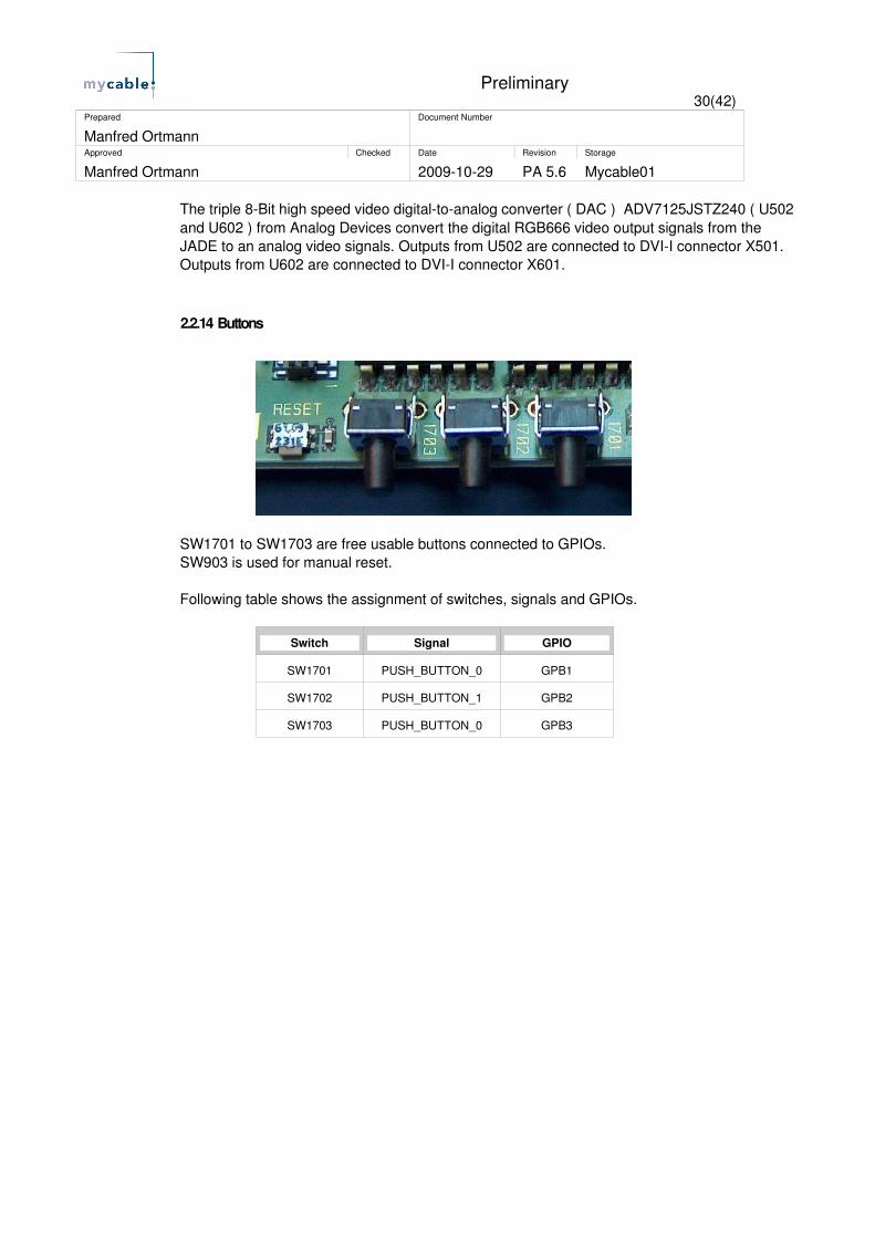
2.2.14 Buttons
SW1701 to SW1703 are free usable buttons connected to GPIOs.SW903 is used for manual reset.
Following table shows the assignment of switches, signals and GPIOs.
Switch Signal GPIO
SW1701 PUSH_BUTTON_0 GPB1
SW1702 PUSH_BUTTON_1 GPB2
SW1703 PUSH_BUTTON_0 GPB3

Preliminary31(42)
Prepared Document Number
Manfred OrtmannApproved Checked Date Revision Storage
Manfred Ortmann 20091029 PA 5.6 Mycable01
2.2.15 LEDs
D1701 and D1703 are free usable LEDs. D1703 is a bicolor LED with red and green. They are connected with buffers ( U1702 ) to GPIOs.A logical '0' switches the LED on. A logical '1' switches the LED off.
Following table shows the assignment of LEDs, signals and GPIOs.
LED Signal GPIO
D1701 LED_3 GPB7
D1702 LED_2 GPB6
D1703 red LED_RED GPA6
D1703 green LED_GREEN GPA7

Preliminary32(42)
Prepared Document Number
Manfred OrtmannApproved Checked Date Revision Storage
Manfred Ortmann 20091029 PA 5.6 Mycable01
2.2.16 Media Oriented Systems Transport ( MOST ) Interface
For the MOST interface the MOST network transceiver device OS81050 ( U1402 ) also called INIC ( Intelligent Network Interface Controller ) from OASIS Silicon Systems is used.
The INIC get the 3.3 V peripheral power supply VDDP and regulates the 2.5 V core ( VDDC ) and analog ( VDDP ) power supply itself by external components.
The oscillator frequency must be 256 times the desired operational frequency of the MOST network, for 44.1 kHz networks 11.2896 MHz and for 48 kHz networks 12.288 Mhz.
The JADE Evaluation board is populated with a 11.2896 Mhz oscillator ( Y1401 ) and a 12.288 MHz oscillator ( Y1402 ) and the assigned resistor R1420 to Y1401 or R1426 to Y1402 has to be populated. As default the 11.2896 Mhz oscillator for 44.1 kHz MOST networks is populated.On prototype boards a resistor is added so a voltage divider is implemented and the level of the clock do not exceed the voltage level for the XTI input of VDDC.
To use the INIC with its Media Local Bus Port ( MLB Port ) dip switch 5 of SW902 has to be set to on.This enables the bus switch FST3125 ( U1403 ) and the MLB Port lines will be connected to the corresponding interface pins of the JADE in function group 2.
Dependent on the application the necessary resistor for the /INTpin 43 and ERR / /BOOTpin 41 of the INIC has to be populated or removed.For details see datasheet of INIC.R1413 to VCC33, enable control port, /INTpin 43R1418 to GND, enable MLB port, /INTpin 43R1409 to VCC, ERR / /BOOTpin 41 R1412 to GND, ERR / /BOOTpin 41 As default all resistors are populated.
On PCB revision PA5 the 0 Ohm resistor R1428 is added. The resistor can be removed if the interrupt shall be disconnected from INT_A2 to use it for extension video out.
Preliminary33(42)
Prepared Document Number
Manfred OrtmannApproved Checked Date Revision Storage
Manfred Ortmann 20091029 PA 5.6 Mycable01
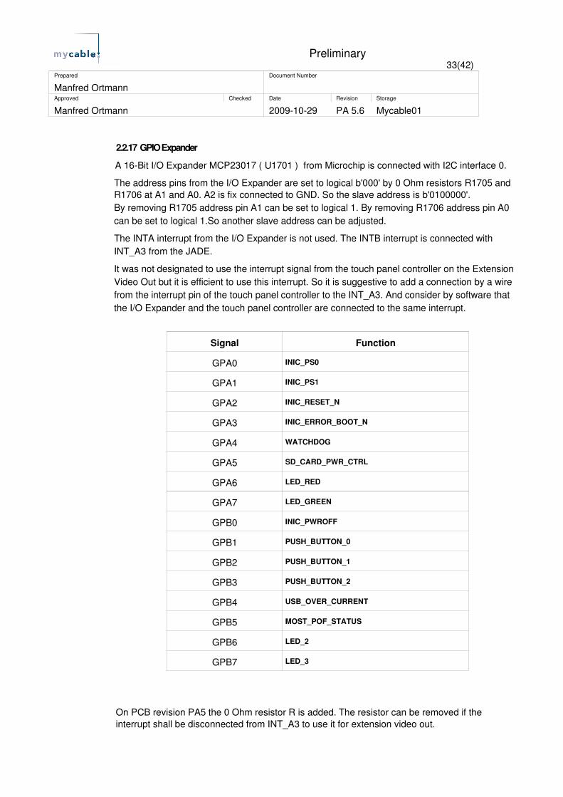
2.2.17 GPIO Expander
A 16Bit I/O Expander MCP23017 ( U1701 ) from Microchip is connected with I2C interface 0.
The address pins from the I/O Expander are set to logical b'000' by 0 Ohm resistors R1705 and R1706 at A1 and A0. A2 is fix connected to GND. So the slave address is b'0100000'.By removing R1705 address pin A1 can be set to logical 1. By removing R1706 address pin A0 can be set to logical 1.So another slave address can be adjusted.
The INTA interrupt from the I/O Expander is not used. The INTB interrupt is connected with INT_A3 from the JADE.
It was not designated to use the interrupt signal from the touch panel controller on the Extension Video Out but it is efficient to use this interrupt. So it is suggestive to add a connection by a wire from the interrupt pin of the touch panel controller to the INT_A3. And consider by software that the I/O Expander and the touch panel controller are connected to the same interrupt.
Signal Function
GPA0 INIC_PS0
GPA1 INIC_PS1
GPA2 INIC_RESET_N
GPA3 INIC_ERROR_BOOT_N
GPA4 WATCHDOG
GPA5 SD_CARD_PWR_CTRL
GPA6 LED_RED
GPA7 LED_GREEN
GPB0 INIC_PWROFF
GPB1 PUSH_BUTTON_0
GPB2 PUSH_BUTTON_1
GPB3 PUSH_BUTTON_2
GPB4 USB_OVER_CURRENT
GPB5 MOST_POF_STATUS
GPB6 LED_2
GPB7 LED_3
On PCB revision PA5 the 0 Ohm resistor R is added. The resistor can be removed if the interrupt shall be disconnected from INT_A3 to use it for extension video out.

Preliminary34(42)
Prepared Document Number
Manfred OrtmannApproved Checked Date Revision Storage
Manfred Ortmann 20091029 PA 5.6 Mycable01
2.2.18 Extension
The extension connector X1200 is implemented especially for the JADE Evaluation Extension Board Video Input. It is not foreseen to use this connector together with the EVBJADED.The functios from the JADE Evaluation Extension Board Video Input will be replaced as far as possible by the EVB JADED Interface board.
All signals have direct connections to the XXSvideo module except signals VCC_IN_OPTIONAL, VCC50 and RESERVED_SW.The filtered input voltage VCC_IN_OPTIONAL and the signal from the not used dip switch RESERVED_SW will not be used at the video input extension board but it is possible to use these signals at extension which are not defined.
Following table shows the pin assignment of the connector X1200. For details see manual from the XXSvideo module.

Preliminary35(42)
Prepared Document Number
Manfred OrtmannApproved Checked Date Revision Storage
Manfred Ortmann 20091029 PA 5.6 Mycable01
Pin Signal Function1 GND Ground2 GND Ground3 VCC50 + 5 V Power Supply4 VCC50 + 5 V Power Supply5 RESET# Reset Input6 INT_A1 Interrupt Output7 VCC_IN_OPTIONAL Optional power supply8 VCC_IN_OPTIONAL Optional power supply9 CPU_D0 CPU Data Bus
10 JADE_IO_G4_13 IDE_XDIOW / 11 GND Ground12 JADE_IO_G4_12 IDE_XDIOR / 13 CPU_D1 CPU Data Bus14 JADE_IO_G4_7 IDE_DA_2 / 15 GND Ground16 JADE_IO_G4_8 IDE_DA_1 / PWMO117 CPU_D2 CPU Data Bus18 JADE_IO_G4_24 IDE_DD_7 / GPIO_PD_1919 GND Ground20 JADE_IO_G4_25 IDE_DD_6 / GPIO_PD_1821 CPU_D3 CPU Data Bus22 JADE_IO_G4_20 IDE_DD_11 / GPIO_PD_2323 GND Ground24 JADE_IO_G4_21 IDE_DD_10 / GPIO_PD_2225 CPU_D4 CPU Data Bus26 JADE_IO_G4_16 IDE_DD_15 / CAN_TX027 GND Ground28 JADE_IO_G4_17 IDE_DD_14 / CAN_RX029 CPU_D5 CPU Data Bus30 JADE_IO_G4_4 IDE_DINTRQ / I2S_SDO131 GND Ground32 JADE_IO_G4_3 IDE_DDMARQ / I2S_ECLK133 CPU_D6 CPU Data Bus34 JADE_IO_G4_6 IDE_DIORDY / 35 GND Ground36 CPU_A1 CPU Address Bus37 CPU_D7 CPU Data Bus38 CPU_A3 CPU Address Bus39 GND Ground40 CPU_A4 CPU Address Bus41 CPU_D8 CPU Data Bus42 CPU_A7 CPU Address Bus43 GND Ground44 CPU_A8 CPU Address Bus45 CPU_D9 CPU Data Bus46 CPU_A11 CPU Address Bus47 GND Ground48 CPU_A12 CPU Address Bus

Preliminary36(42)
Prepared Document Number
Manfred OrtmannApproved Checked Date Revision Storage
Manfred Ortmann 20091029 PA 5.6 Mycable01
49 CPU_D10 CPU Data Bus50 CPU_A15 CPU Address Bus51 CPU_D11 CPU Data Bus52 CPU_A15 CPU Address Bus53 CPU_D15 CPU Data Bus54 CPU_A19 CPU Address Bus55 CPU_D12 CPU Data Bus56 CPU_A20 CPU Address Bus57 CPU_D14 CPU Data Bus58 CPU_A23 CPU Address Bus59 CPU_D13 CPU Data Bus60 MEM_XWR1 CPU Write 1 enable61 JADE_IO_G2_13 VIN1_1 / GI1_7 / I2S_SCK1 / I2S_SCK1 / I2S_SCK162 RESERVED_SW Signal from DIP switch
63 JADE_IO_G2_4VINVSYNC1 / VINVSYNC1 / I2S_ECLK1 / I2S_ECLK1 / I2S_ECLK1
64 JADE_IO_G2_2 VINFID0 / GI1_3 / MLB_CLK / MLB_CLK / MLB_CLK65 JADE_IO_G2_21 I2S_SDI0 / BI1_2 / I2S_SDI2 / SPI_DI / I2S_SDI2
66 JADE_IO_G2_0VINVSYNC0 / GI1_5 / MLB_DATA / MLB_DATA / MLB_DATA
67 JADE_IO_G2_11 VIN1_3 / RI1_3 / CAN_TX1 / CAN_TX1 / CAN_TX1
68 JADE_IO_G2_8VIN1_6 / RI1_6 / GPIO_PD_4 / GPIO_PD_4 / GPIO_PD_4
69 JADE_IO_G2_14 VIN1_0 / GI1_6 / I2S_WS1 / I2S_WS1 / I2S_WS1
70 JADE_IO_G2_1VINHSYNC0 / GI1_4 / MLB_SIG / MLB_SIG / MLB_SIG
71 JADE_IO_G2_5VINHSYNC1 / VINHSYNC1 / I2S_SDI1 / I2S_SDI1 / I2S_SDI1
72 JADE_IO_G2_7VIN1_7 / RI1_7 / GPIO_PD_5 / GPIO_PD_5 / GPIO_PD_5
73 JADE_IO_G2_20 I2SWS0 / BI1_3 / I2S_WS2 / SPI_SS / I2S_WS274 JADE_IO_G2_9 VIN1_5 / RI1_5 / CAN_TX0 / CAN_TX0 / CAN_TX075 JADE_IO_G4_10 IDE_XDCS_1 / 76 JADE_IO_G2_10 VIN1_4 / RI1_4 / CAN_RX0 / CAN_RX0 / CAN_RX077 JADE_IO_G4_11 IDE_XDCS_0 / 78 MEM_XRD CPU Read enable79 JADE_IO_G4_14 IDE_CSEL / 80 MEM_XCS2 CPU Chip select 281 JADE_IO_G4_9 IDE_DA_0 / PWMO082 CPU_A22 CPU Address Bus83 JADE_IO_G4_27 IDE_DD_4 / GPIO_PD_1684 CPU_A21 CPU Address Bus85 JADE_IO_G4_26 IDE_DD_5 / GPIO_PD_1786 MEM_XWR0 CPU Write 0 enable87 JADE_IO_G4_23 IDE_DD_8 / GPIO_PD_2088 CPU_A24 CPU Address Bus89 JADE_IO_G4_22 IDE_DD_9 / GPIO_PD_2190 MEM_RDY CPU Memory ready91 JADE_IO_G4_19 IDE_DD_12 / CAN_RX192 |2C_1_0 |2C_SCL193 JADE_IO_G4_18 IDE_DD_13 / CAN_TX1

Preliminary37(42)
Prepared Document Number
Manfred OrtmannApproved Checked Date Revision Storage
Manfred Ortmann 20091029 PA 5.6 Mycable01
94 |2C_1_1 |2C_SDA195 JADE_IO_G4_15 IDE_XDDMACK / 96 CPU_A2 CPU Address Bus97 JADE_IO_G4_0 IDE_XDRESET / 98 CPU_A6 CPU Address Bus99 JADE_IO_G4_2 IDE_XDASP / I2S_WS1
100 CPU_A5 CPU Address Bus101 JADE_IO_G4_1 IDE_XIOCS16 / I2S_SDI1102 CPU_A10103 JADE_IO_G4_5 IDE_XCBLID / I2S_SCK1104 CPU_A9 CPU Address Bus
105 JADE_IO_G2_15PWMO0 / GI1_2 / GPIO_PD_3 / GPIO_PD_3 / GPIO_PD_3
106 CPU_A14 CPU Address Bus
107 JADE_IO_G2_18I2S_ECLK0 / BI1_5 / I2S_ECLK2 / reserved / GPIO_PD_0
108 CPU_A13 CPU Address Bus
109 JADE_IO_G2_16PWMO1 / BI1_7 / GPIO_PD_2 / GPIO_PD_2 / GPIO_PD_2
110 CPU_A18 CPU Address Bus
111 JADE_IO_G2_19I2S_SCK0 / BI1_4 / I2S_SCK2 / SPI_SCK / I2S_SCK2
112 CPU_A17 CPU Address Bus
113 JADE_IO_G2_17I2S_SDO0 / BI1_6 / I2S_SDO2 / SPI_DO / GPIO_PD_1
114 JADE_IO_G4_28 IDE_DD_3 / GPIO_PD_15
115 JADE_IO_G2_6VINFID1 / VINFID1 / I2S_SDO1 / I2S_SDO1 / I2S_SDO1
116 JADE_IO_G4_29 IDE_DD_2 / GPIO_PD_14117 JADE_IO_G2_3 CCLK1118 JADE_IO_G4_30 IDE_DD_1 / GPIO_PD_13119 JADE_IO_G2_12 VIN1_2 / RI1_2 / CAN_RX1 / CAN_RX1 / CAN_RX1120 JADE_IO_G4_31 IDE_DD_0 / 121 GND Ground122 GND Ground123 GND Ground124 GND Ground125 GND Ground126 GND Ground127 GND Ground128 GND Ground

Preliminary38(42)
Prepared Document Number
Manfred OrtmannApproved Checked Date Revision Storage
Manfred Ortmann 20091029 PA 5.6 Mycable01
2.2.19 Secure Digital ( SD ) Memory Card Interface
The following description of the video outputs is relevant if a XXSvideo module is used.If a EVBJADED is used see manual of this board.
At SD memory card connector X1501 the signals of the SD memory card from the JADE are connected.
The supply voltage SD_CARD_VCC for the SD memory card will be switched from GPIO GPA5. A logical 0 at GPIO GPA5 switchs the supply voltage ON.
Following table shows the assignment of pins, signals and function.
Pin Signal Function
1 SD_DAT3 SD data line 3
2 SD_CMD Command line
3 GND Ground
4 SD_CARD_VCC Supply voltage
5 SD_CLK Clock
6 GND Ground
7 SD_DAT0 SD data line 0
8 SD_DAT1 SD data line 1
9 SD_DAT2 SD data line 2
10 SD_XMCD Card detect
11 VCC33 3.3 V Supply voltage
12 SD_WP Write protect

Preliminary39(42)
Prepared Document Number
Manfred OrtmannApproved Checked Date Revision Storage
Manfred Ortmann 20091029 PA 5.6 Mycable01
2.3 Hardware Variants
Prototypes have the version PA2. Nearly all functions work without modifications.Only for the function of the push buttons and for the function of the MOST interface modifications are necessary. These errors are corrected with version PA4.Changes of version PA5 are described in the relevant chapters. For overview see revision history.

Preliminary40(42)
Prepared Document Number
Manfred OrtmannApproved Checked Date Revision Storage
Manfred Ortmann 20091029 PA 5.6 Mycable01
2.4 Placement of Components
The placement of components on the JADE Evaluation board is shown below.
Pictures from placement of components with a better resolution are available as separate pdf documents.

Preliminary41(42)
Prepared Document Number
Manfred OrtmannApproved Checked Date Revision Storage
Manfred Ortmann 20091029 PA 5.6 Mycable01

Preliminary42(42)
Prepared Document Number
Manfred OrtmannApproved Checked Date Revision Storage
Manfred Ortmann 20091029 PA 5.6 Mycable01
2.5 Mechanical Dimensions
The JADE Evaluation board has a size of 165.0 x 100.0 mm.
Pictures from mechanical dimensions with a better resolution are available as separate pdf documents.