managing device i/o pins - intel.com · to assign i/o pins in the pin planner, follow these steps:...
TRANSCRIPT
4Managing Device I/O Pins
2013.11.04
QII52013 Subscribe Send Feedback
This document describes efficient planning and assignment of the I/O pins in your target device. You shouldconsider I/O standards, pin placement rules, and your PCB characteristics early in the design phase.
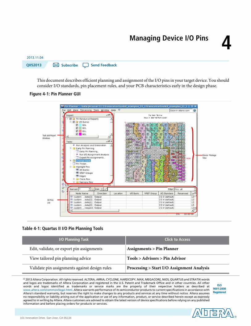
Figure 4-1: Pin Planner GUI
Task and ReportWindows
All PinsList
Device PackageView
Table 4-1: Quartus II I/O Pin Planning Tools
Click to AccessI/O Planning Task
Assignments > Pin PlannerEdit, validate, or export pin assignments
Tools > Advisors > Pin AdvisorView tailored pin planning advice
Processing > Start I/O Assignment AnalysisValidate pin assignments against design rules
ISO9001:2008Registered
© 2013 Altera Corporation. All rights reserved. ALTERA, ARRIA, CYCLONE, HARDCOPY, MAX, MEGACORE, NIOS, QUARTUS and STRATIX wordsand logos are trademarks of Altera Corporation and registered in the U.S. Patent and Trademark Office and in other countries. All otherwords and logos identified as trademarks or service marks are the property of their respective holders as described atwww.altera.com/common/legal.html. Altera warrants performance of its semiconductor products to current specifications in accordance withAltera's standard warranty, but reserves the right to make changes to any products and services at any time without notice. Altera assumesno responsibility or liability arising out of the application or use of any information, product, or service described herein except as expresslyagreed to in writing by Altera. Altera customers are advised to obtain the latest version of device specifications before relying on any publishedinformation and before placing orders for products or services.
www.altera.com
101 Innovation Drive, San Jose, CA 95134
I/O Planning OverviewYou should plan and assign I/O pins in your design for compatibility with your target device and PCBcharacteristics. Plan I/O pins early to reduce design iterations and develop an accurate PCB layout sooner.You can assign expected nodes not yet defined in design files, including interface IP core signals, and thengenerate a top-level file. Specify interfaces formemory, high-speed I/O, device configuration, and debuggingtools in your top-level file. The top-level file instantiates the next level of design hierarchy and includesinterface port information.
Use the Pin Planner to view, assign, and validate device I/O pin logic and properties. Alternatively, you canenter I/O assignments in a Tcl script, or directly in HDL code. The Pin Planner Task window provides one-click access to I/O planning steps. You can filter and search the nodes in the design. You can define customgroups of pins for assignment. Instantly locate and highlight specific pin types for assignment or evaluation,such as I/O banks, VREF groups, edges, DQ/DQS pins, hard memory interface pins, PCIe hard IP interfacepins, hard processor systempins, and clock region input pins. Assign design elements, I/O standards, interfaceIP, and other properties to the device I/O pins by name or by drag and drop. You can then generate a top-level design file for I/O validation.
Use live I/O check to verify the legality of pin assignments in real time. Use I/O assignment analysis to runa full I/O analysis against VCCIO,VREF, electromigration (current density), Simultaneous SwitchingOutput(SSO), drive strength, I/O standard, PCI_IO clamp diode, and I/O pin direction compatibility rules.
Basic I/O Planning FlowThe following steps describe the basic flow for assigning and verifying I/O pin assignments:
1. Click Assignments > Device and select a target device that meets your logic, performance, and I/Orequirements. Consider and specify /O standards, voltage and power supply requirements, and availableI/O pins.
2. Click Assignments > Pin Planner.3. To setup a top-level HDL wrapper file that defines early port and interface information for your design,
click Early Pin Planning in the Tasks pane.
a. Click Create/Import IP Core and define the parameters of any expected interface IP core, and thenassign signals to the interface IP nodes.
b. Click Set Up Top-Level File and assign user nodes to device pins. User nodes become virtual pins inthe top-level file and are not assigned to device pins.
c. Click Generate Top-Level File. Use this file to validate I/O assignments.
4. Click Run I/O Assignment Analysis in the Tasks pane to validate any early assignments and generate asynthesized design netlist.
5. Assign I/O properties to match your device and PCB characteristics, including assigning logic, I/Ostandards, output loading, slew rate, and current strength.
6. ClickRun I/OAssignmentAnalysis in the Tasks pane to validate assignments and generate a synthesizeddesign netlist. Correct any problems reported.
7. ClickProcessing>StartCompilation. During compilation, theQuartus II software runs I/O assignmentanalysis and advanced I/O timing analysis.
Managing Device I/O PinsAltera Corporation
Send Feedback
QII52013I/O Planning Overview4-2 2013.11.04
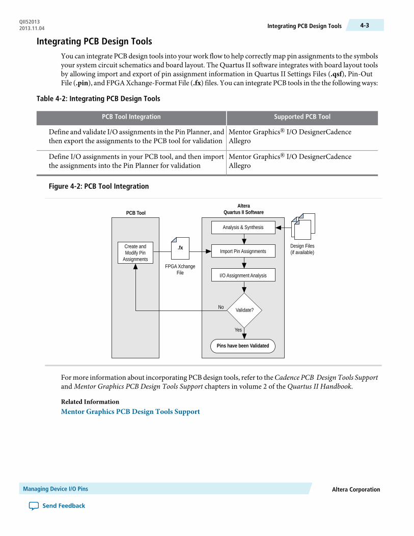
Integrating PCB Design ToolsYou can integrate PCB design tools into your work flow to help correctlymap pin assignments to the symbolsyour system circuit schematics and board layout. The Quartus II software integrates with board layout toolsby allowing import and export of pin assignment information in Quartus II Settings Files (.qsf), Pin-OutFile (.pin), and FPGAXchange-Format File (.fx) files. You can integrate PCB tools in the the followingways:
Table 4-2: Integrating PCB Design Tools
Supported PCB ToolPCB Tool Integration
Mentor Graphics® I/O DesignerCadenceAllegro
Define and validate I/O assignments in the Pin Planner, andthen export the assignments to the PCB tool for validation
Mentor Graphics® I/O DesignerCadenceAllegro
Define I/O assignments in your PCB tool, and then importthe assignments into the Pin Planner for validation
Figure 4-2: PCB Tool Integration
Create andModify PinAssignments
PCB Tool
I/O Assignment Analysis
Validate?
AlteraQuartus II Software
Import Pin AssignmentsDesign Files(if available)
Yes
No
Analysis & Synthesis
Pins have been Validated
FPGA XchangeFile
.fx
Formore information about incorporating PCB design tools, refer to theCadence PCB Design Tools Supportand Mentor Graphics PCB Design Tools Support chapters in volume 2 of the Quartus II Handbook.
Related InformationMentor Graphics PCB Design Tools Support
Altera CorporationManaging Device I/O Pins
Send Feedback
4-3Integrating PCB Design ToolsQII520132013.11.04

Altera Device TermsThe following terms describe Altera device and I/O structures:
Assigning I/O PinsUse the Pin Planner to visualize, modify, and validate I/O assignments in a graphical representation of thetarget device. To assign I/O pins, locate the device I/O pin(s) for assignment, enter properties for the pin(s),and validate the legality of the assignment. You can increase the accuracy of I/O assignment analysis byreserving specific device pins to accommodate undefined but expected I/O.
Managing Device I/O PinsAltera Corporation
Send Feedback
QII52013Altera Device Terms4-4 2013.11.04
To assign I/O pins in the Pin Planner, follow these steps:
1. Open a Quartus II project, and then click Assignments > Pin Planner.2. (Optional) To validate I/O pin assignments in real time, click Processing > Enable Live I/O Check.3. Click Processing > Start Analysis & Elaboration to elaborate the design and display All Pins in the
device view.4. To locate or highlight pins for assignment, click Pin Finder or a pin type under Highlight Pins in the
Tasks pane.5. (Optional) To define a custom group of nodes for assignment, select one or more nodes in the Groups
or All Pins list, and then click Create Group.6. Enter assignments of logic, I/O standards, interface IP, and properties for device I/O pins in the All Pins
spreadsheet, or by drag and drop into the package view.7. To assign properties to differential pin pairs, click Show Differential Pin Pair Connections. A red
connection line appears between positive (p) and negative (n) differential pins.8. (Optional) To create board trace model assignments, right-click an output or bidirectional pin, and then
click Board Trace Model. For differential I/O standards, the board trace model uses a differential pinpair with two symmetrical board trace models. Specify board trace parameters on the positive end of thedifferential pin pair. The assignment applies to the corresponding value on the negative end of thedifferential pin pair.
9. To run a full I/O assignment analysis, click Run I/O Assignment Analysis. The Fitter reports analysisresults. Only reserved pins are analyzed prior to design synthesis.
Assigning to Exclusive Pin GroupsYou can designate groups of pins for exclusive assignment.When you assign pins to anExclusive I/OGroup,the Fitter does not place the signals in the same I/O bank with any other exclusive I/O group. For example,if you have a set of signals assigned exclusively togroup_a, and another set of signals assigned togroup_b,the Fitter ensures placement of each group in different I/O banks.
Assigning Slew Rate and Drive StrengthYou can designate the device pin slew rate and drive strength. These properties affect the pin’s outgoingsignal integrity. Use either the Slew Rate or Slow Slew Rate assignment to adjust the drive strength of a pinwith the Current Strength assignment. The slew rate and drive strength apply during live I/O check andI/O assignment analysis.
Assigning Differential PinsWhen you use the Pin Planner to assign a differential I/O standard to a single-ended top-level pin in yourdesign, it automatically recognizes the negative pin as part of the differential pin pair assignment and createsthe negative pin for you. The Quartus II software writes the location assignment for the negative pin to the.qsf; however, the I/O standard assignment is not added to the .qsf for the negative pin of the differentialpair.
The following example shows a design with lvds_in top-level pin, to which you assign a differential I/Ostandard. The Pin Planner automatically creates the differential pin, lvds_in(n) to complete thedifferential pin pair.
Altera CorporationManaging Device I/O Pins
Send Feedback
4-5Assigning to Exclusive Pin GroupsQII520132013.11.04
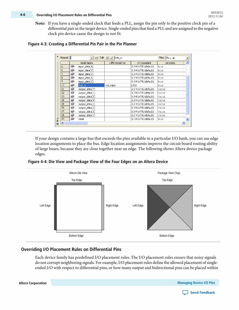
If you have a single-ended clock that feeds a PLL, assign the pin only to the positive clock pin of adifferential pair in the target device. Single-ended pins that feed a PLL and are assigned to the negativeclock pin device cause the design to not fit.
Note:
Figure 4-3: Creating a Differential Pin Pair in the Pin Planner
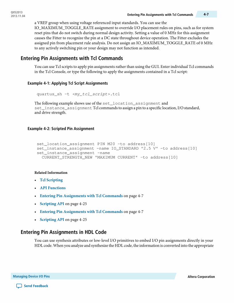
If your design contains a large bus that exceeds the pins available in a particular I/O bank, you can use edgelocation assignments to place the bus. Edge location assignments improve the circuit board routing abilityof large buses, because they are close together near an edge. The following shows Altera device packageedges.
Figure 4-4: Die View and Package View of the Four Edges on an Altera Device
Top Edge
Silicon Die View
Bottom Edge
Left Edge Right Edge Right Edge
Top Edge
Package View (Top)
Bottom Edge
Left Edge
Overriding I/O Placement Rules on Differential Pins
Each device family has predefined I/O placement rules. The I/O placement rules ensure that noisy signalsdo not corrupt neighboring signals. For example, I/O placement rules define the allowed placement of single-ended I/O with respect to differential pins, or how many output and bidirectional pins can be placed within
Managing Device I/O PinsAltera Corporation
Send Feedback
QII52013Overriding I/O Placement Rules on Differential Pins4-6 2013.11.04
a VREF group when using voltage referenced input standards. You can use theIO_MAXIMUM_TOGGLE_RATE assignment to override I/O placement rules on pins, such as for systemreset pins that do not switch during normal design activity. Setting a value of 0 MHz for this assignmentcauses the Fitter to recognize the pin at a DC state throughout device operation. The Fitter excludes theassigned pin from placement rule analysis. Do not assign an IO_MAXIMUM_TOGGLE_RATE of 0 MHzto any actively switching pin or your design may not function as intended.
Entering Pin Assignments with Tcl CommandsYou can use Tcl scripts to apply pin assignments rather than using the GUI. Enter individual Tcl commandsin the Tcl Console, or type the following to apply the assignments contained in a Tcl script:
Example 4-1: Applying Tcl Script Assignments
quartus_sh -t <my_tcl_script>.tcl
The following example shows use of the set_location_assignment andset_instance_assignmentTcl commands to assign a pin to a specific location, I/O standard,and drive strength.
Example 4-2: Scripted Pin Assignment
set_location_assignment PIN M20 -to address[10]set_instance_assignment -name IO_STANDARD "2.5 V" -to address[10]set_instance_assignment -name CURRENT_STRENGTH_NEW "MAXIMUM CURRENT" -to address[10]
Related Information
• Tcl Scripting
• API Functions
• Entering Pin Assignments with Tcl Commands on page 4-7
• Scripting API on page 4-25
• Entering Pin Assignments with Tcl Commands on page 4-7
• Scripting API on page 4-25
Entering Pin Assignments in HDL CodeYou can use synthesis attributes or low-level I/O primitives to embed I/O pin assignments directly in yourHDL code.When you analyze and synthesize theHDL code, the information is converted into the appropriate
Altera CorporationManaging Device I/O Pins
Send Feedback
4-7Entering Pin Assignments with Tcl CommandsQII520132013.11.04
I/O pin assignments. You can use either of the following methods to specify pin-related assignments withHDL code:
• Assigning synthesis attributes for signal names that are top-level pins• Using low-level I/O primitives, such as ALT_BUF_IN, to specify input, output, and differential buffers,
and for setting parameters or attributes
Using Synthesis Attributes
The Quartus II software translates synthesis attributes into standard assignments during compilation. Theassignments appear in the Pin Planner. If you modify or delete these assignments in the Pin Planner andthen recompile your design, the Pin Planner changes override the synthesis attributes. Quartus II synthesissupports the chip_pin, useioff, and altera_attribute synthesis attributes.
Use the chip_pin and useioff synthesis attributes to create pin location assignments and to assignFast Input Register, Fast Output Register, and Fast Output Enable Register logic options. The followingexamples use the chip_pin and useioff attributes to embed location and Fast Input Register logicoption assignments in Verilog HDL and VHDL design files.
Example 4-3: Verilog HDL Synthesis Attribute
input my_pin1 /* synthesis altera_attribute = "-name FAST_INPUT_REGISTER ON; -name IO_STANDARD \"2.5 V\" " */ ;
Example 4-4: VHDL Synthesis Attribute
VHDL Exampleentity my_entity is port( my_pin1: in std_logic );end my_entity;
architecture rtl of my_entity isattribute useioff : boolean;attribute useioff of my_pin1 : signal is true;attribute chip_pin : string;attribute chip_pin of my_pin1 : signal is "C1";begin -- The architecture body end rtl;
Use the altera_attribute synthesis attribute to create other pin-related assignments in yourHDL code. The altera_attribute attribute is understood only by Quartus II integratedsynthesis and supports all types of instance assignments. The following examples use thealtera_attribute attribute to embed Fast Input Register logic option assignments and I/Ostandard assignments in both a Verilog HDL and a VHDL design file.
Managing Device I/O PinsAltera Corporation
Send Feedback
QII52013Using Synthesis Attributes4-8 2013.11.04

Example 4-5: Verilog HDL Synthesis Attribute
input my_pin1 /* synthesis chip_pin = "C1" useioff = 1 */;
Example 4-6: VHDL Synthesis Attribute
entity my_entity is port( my_pin1: in std_logic );end my_entity;architecture rtl of my_entity is begin
attribute altera_attribute : string;attribute altera_attribute of my_pin1: signal is "-name FAST_INPUT_REGISTER ON;-- The architecture body end rtl;
Using Low-Level I/O Primitives
You can alternatively enter I/O pin assignments using low-level I/O primitives. You can assign pin locations,I/O standards, drive strengths, slew rates, and on-chip termination (OCT) value assignments. You can alsouse low-level differential I/O primitives to define both positive and negative pins of a differential pair in theHDL code for your design.
Primitive-based assignments do not appear in the Pin Planner until after you perform a full compilationand back-annotate pin assignments (Assignments > Back Annotate Assignments).
Related InformationDesigning with Low Level Primitives User Guide
Altera CorporationManaging Device I/O Pins
Send Feedback
4-9Using Low-Level I/O PrimitivesQII520132013.11.04
Importing and Exporting I/O Pin AssignmentsThe Quartus II software supports transfer of I/O pin assignments across projects, or for analysis in third-party PCB tools. You can import or export I/O pin assignments in the following ways:
Table 4-3: Importing and Exporting I/O Pin Assignments
Export AssignmentsImport Assignments
• From Quartus II project for optimizationin a PCB design tool
• From Quartus II project for spreadsheetanalysis or use in scripting assignments
• From Quartus II project for import intoanother Quartus II project with similarconstraints
• From your PCB design tool orspreadsheet into Pin Planner duringearly pin planning or after optimizationin PCB tool
• From another Quartus II project withcommon constraints
Scenario
Assignments > Export AssignmentsAssignments > Import AssignmentsCommand
.pin, .fx, .csv, .tcl, .qsf.qsf, .esf, .acf, .csv, .txt, .sdcFile formats
Exported .csv files retain column and roworder and format. Do not modify the row ofcolumn headings if importing the .csv file
N/ANotes
Importing and Exporting for PCB ToolsThe Pin Planner supports import and export of assignmentswith PCB tools. You can export valid assignmentsas a .pin file for analysis in other supported PCB tools. You can also import optimized assignment fromsupported PCB tools. The .pin file contains pin name, number, and detailed properties.
Mentor Graphics I/O Designer requires you to generate and import both an .fx and a .pin file to transferassignments. However, the Quartus II software requires only the .fx to import pin assignments from I/ODesigner.
Table 4-4: Contents of .pin File
DescriptionFile Column Name
The name of the design pin, or whether the pin is GND or VCC pinPin Name/Usage
The pin number of the location on the device packageLocation
The direction of the pinDir
The name of the I/O standard to which the pin is configuredI/O Standard
The voltage level that is required to be connected to the pinVoltage
The I/O bank to which the pin belongsI/O Bank
Managing Device I/O PinsAltera Corporation
Send Feedback
QII52013Importing and Exporting I/O Pin Assignments4-10 2013.11.04

DescriptionFile Column Name
Y or N indicating if the location assignment for the design pin was userassigned (Y) or assigned by the Fitter (N)
User Assignment
Related Information
• Pin-Out Files for Altera Devices
• Mentor Graphics PCB Tools Support
Migrating Assignments to Another Target DeviceYou canmigrate compatible pin assignments fromone target device to another. You canmigrate to a differentdensity and the same device package. You can also migrate between device packages with different densitiesand pin counts. ClickView>PinMigrationWindow to verify whether your pin assignments are compatiblewith migration to a different Altera device.
The Quartus II software ignores invalid assignments and generates an error message during compilation.After evaluating migration compatibility, modify any incompatible assignments, and then click Export toexport the assignments to another project.
Altera CorporationManaging Device I/O Pins
Send Feedback
4-11Migrating Assignments to Another Target DeviceQII520132013.11.04
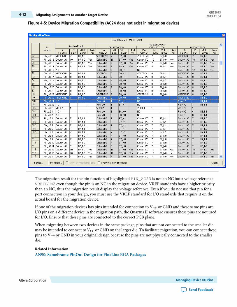
Figure 4-5: Device Migration Compatibility (AC24 does not exist in migration device)
The migration result for the pin function of highlighted PIN_AC23 is not an NC but a voltage referenceVREFB1N2 even though the pin is an NC in the migration device. VREF standards have a higher prioritythan an NC, thus the migration result display the voltage reference. Even if you do not use that pin for aport connection in your design, you must use the VREF standard for I/O standards that require it on theactual board for the migration device.
If one of the migration devices has pins intended for connection to VCC or GND and these same pins areI/O pins on a different device in the migration path, the Quartus II software ensures these pins are not usedfor I/O. Ensure that these pins are connected to the correct PCB plane.
When migrating between two devices in the same package, pins that are not connected to the smaller diemay be intended to connect to VCC or GND on the larger die. To facilitate migration, you can connect thesepins to VCC or GND in your original design because the pins are not physically connected to the smallerdie.
Related InformationAN90: SameFrame PinOut Design for FineLine BGA Packages
Managing Device I/O PinsAltera Corporation
Send Feedback
QII52013Migrating Assignments to Another Target Device4-12 2013.11.04
Validating Pin AssignmentsThe Quartus II software validates I/O pin assignments against predefined I/O rules for your target device.You can use the following tools to validate your I/O pin assignments throughout the pin planning process:
Table 4-5: I/O Validation Tools
Click to RunDescriptionI/O Validation Tool
Processing > Enable Live I/O CheckVerifies preliminary, basic I/O legality as youenter assignments
Live I/OCheck
Processing > Start I/O AssignmentAnalysis
Verifies I/O assignment legality of synthesizeddesign against full set of I/O rules for the targetdevice
I/OAssignmentAnalysis
Processing > Start CompilationFully validates I/O assignments against all I/Oand timing checks during compilation
Advanced I/OTiming
I/O Assignment Validation RulesI/O Assignment Analysis validates your assignments against the following rules:
Table 4-6: Examples of I/O Rule Checks
HDL Required?DescriptionRule
NoChecks the number of pins assigned to an I/O bankagainst the number of pins allowed in the I/O bank.
I/O bank capacity
NoChecks that no more than one VCCIO is required forthe pins assigned to the I/O bank.
I/O bank VCCIO voltage compati-bility
NoChecks that no more than one VREF is required for thepins assigned to the I/O bank.
I/O bank VREF voltage compati-bility
NoChecks whether the pin location supports the assignedI/O standard.
I/O standard and location conflicts
NoChecks whether the pin location supports the assignedI/O standard and direction. For example, certain I/Ostandards on a particular pin location can only supportoutput pins.
I/O standard and signal directionconflicts
NoChecks that open drain is turned off for all pins with adifferential I/O standard.
Differential I/O standards cannothave open drain turned on
NoChecks whether the drive strength assignments arewithin the specifications of the I/O standard.
I/O standard and drive strengthconflicts
Altera CorporationManaging Device I/O Pins
Send Feedback
4-13Validating Pin AssignmentsQII520132013.11.04

HDL Required?DescriptionRule
NoChecks whether the pin location supports the assigneddrive strength.
Drive strength and location conflicts
NoChecks whether the pin location supports BUSHOLD.For example, dedicated clock pins do not supportBUSHOLD.
BUSHOLD and location conflicts
NoChecks whether the pin location supports WEAK_PULLUP (for example, dedicated clock pins do notsupport WEAK_PULLUP).
WEAK_PULLUP and locationconflicts
NoChecks whether combined drive strength of consecutivepads exceeds a certain limit. For example, the totalcurrent drive for 10 consecutive pads on a Stratix IIdevice cannot exceed 200 mA.
Electromigration check
NoChecks whether the pin location along with the I/Ostandard assigned supports PCI_IO clamp diode.
PCI_IO clamp diode, location, andI/O standard conflicts
YesChecks that all pins connected to a SERDES in yourdesign are assigned to dedicated SERDES pin locations.
SERDES and I/O pin locationcompatibility check
YesChecks whether pins connected to a PLL are assignedto the dedicated PLL pin locations.
PLL and I/O pin location compati-bility check
Table 4-7: Signal Switching Noise Rules
HDL Required?DescriptionRule
NoChecks that no single-ended I/O pin exists in the sameI/O bank as a DPA.
I/O bank can not have single-endedI/O when DPA exists
NoChecks that there are no single-ended I/O pins presentin the PLL I/O Bank when a differential signal exists.
A PLL I/O bank does not supportboth a single-ended I/O and adifferential signal simultaneously
NoChecks whether single-ended output pins are a certaindistance away from a differential I/O pin.
Single-ended output is required tobe a certain distance away from adifferential I/O pin
NoChecks whether single-ended output pins are a certaindistance away from a VREF pad.
Single-ended output has to be acertain distance away from a VREFpad
NoChecks whether single-ended input pins are a certaindistance away from a differential I/O pin.
Single-ended input is required to bea certain distance away from adifferential I/O pin
Managing Device I/O PinsAltera Corporation
Send Feedback
QII52013I/O Assignment Validation Rules4-14 2013.11.04
HDL Required?DescriptionRule
NoChecks that there are no more than a certain number ofoutputs or bidirectional pins in a VREFGROUP whena VREF is used.
Too many outputs or bidirectionalpins in a VREFGROUP when aVREF is used
NoChecks whether too many outputs are in aVREFGROUP.
Too many outputs in aVREFGROUP
Checking I/O Pin Assignments In Real-TimeLive I/O check validates I/O assignments against basic I/O buffer rules in real time. The Pin Plannerimmediately reports warnings or errors about assignments as you enter them. The Live I/O Check Statuswindow displays the total number of errors and warnings. Use this analysis to quickly correct basic errorsbefore proceeding. Run full I/O assignment analysis when you are ready to validate pin assignments againstthe complete set of I/O system rules.
Live I/O check validates against the following basic I/O buffer rules:
• VCCIO and VREF voltage compatibility rules• Electromigration (current density) rules• Simultaneous Switching Output (SSO) rules• I/Oproperty compatibility rules, such as drive strength compatibility, I/O standard compatibility,PCI_IO
clamp diode compatibility, and I/O direction compatibility• Illegal location assignments:
• An I/O bank or VREF group with no available pins• The negative pin of a differential pair if the positive pin of the differential pair is assigned with a node
name with a differential I/O standard• Pin locations that do not support the I/O standard assigned to the selected node name• For HSTL- and SSTL-type I/O standards, VREF groups of a different VREF voltage than the selected
node name.
Live I/O check is supported only for .28nm and larger device families.Note:
Related InformationAssigning Device I/O Pins in Pin Planner
Running I/O Assignment AnalysisI/O assignment analysis validates I/O assignments against the complete set of I/O system and board layoutrules. Full I/O assignment analysis validates blocks that directly feed or are fed by resources such as a PLL,LVDS, or gigabit transceiver blocks. In addition, the checker validates the legality of proper VREF pin use,pin locations, and acceptable mixed I/O standards
Run I/O assignment analysis during early pin planning to validate initial reserved pin assignments beforecompilation. Once you define design files, run I/O assignment analysis to perform more thorough legalitychecks with respect to the synthesized netlist. Run I/O assignment analysis whenever you modify I/Oassignments.
Altera CorporationManaging Device I/O Pins
Send Feedback
4-15Checking I/O Pin Assignments In Real-TimeQII520132013.11.04
The Fitter assigns pins to accommodate your constraints. For example, if you assign an edge location to agroup of LVDS pins, the Fitter assigns pin locations for each LVDS pin in the specified edge location andthen performs legality checks. To display the Fitter-placed pins, click Show Fitter Placements in the PinPlanner. To accept these suggested pin locations, you must back-annotate your pin assignments.
View the I/O Assignment Warnings report to view and resolve all assignment warnings. For example, awarning that some design pins have undefined drive strength or slew rate. The Fitter recognizes undefined,single-ended output and bidirectional pins as non-calibratedOCT. To resolve thewarning, assign theCurrentStrength, SlewRate or SlowSlewRate for the reported pin. Alternatively, you could assign theTerminationto the pin. You cannot assign drive strength or slew rate settings when a pin has an OCT assignment.
Related InformationBack-Annotating Assignments for A Project
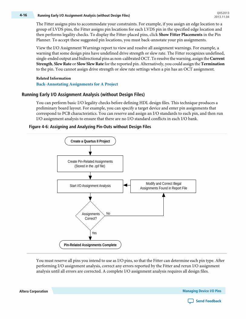
Running Early I/O Assignment Analysis (without Design Files)
You can perform basic I/O legality checks before defining HDL design files. This technique produces apreliminary board layout. For example, you can specify a target device and enter pin assignments thatcorrespond to PCB characteristics. You can reserve and assign an I/O standards to each pin, and then runI/O assignment analysis to ensure that there are no I/O standard conflicts in each I/O bank.
Figure 4-6: Assigning and Analyzing Pin-Outs without Design Files
Modify and Correct IllegalAssignments Found in Report File
Create Pin-Related Assignments(Stored in the .qsf file)
Start I/O Assignment Analysis
Create a Quartus II Project
Pin-Related Assignments Complete
Yes
NoAssignmentsCorrect?
You must reserve all pins you intend to use as I/O pins, so that the Fitter can determine each pin type. Afterperforming I/O assignment analysis, correct any errors reported by the Fitter and rerun I/O assignmentanalysis until all errors are corrected. A complete I/O assignment analysis requires all design files.
Managing Device I/O PinsAltera Corporation
Send Feedback
QII52013Running Early I/O Assignment Analysis (without Design Files)4-16 2013.11.04

Running I/O Assignment Analysis (with Design Files)
Use I/O assignment analysis to perform full I/O legality checks after fully defining HDL design files. Whenyou run I/O assignment analysis on a complete design, the tool verifies all I/O pin assignments against allI/O rules. When you run I/O assignment analysis on a partial designs, the tool checks legality only for definedportions of the design. The following figure shows the work flow for analyzing pin-outs with design files.
Figure 4-7: I/O Assignment Analysis Flow
Modify and Correct IllegalAssignments Found in Report File
Create Pin-Related Assignments(Stored in the .qsf file)
Start I/O Assignment Analysis
Back-Annotate I/O AssignmentAnalysis Pin Placements
Perform Analysis & Synthesisto Create a Mapped Netlist
Open a Quartus II Project or Design File
Pin-Related Assignments Complete
Yes
NoAssignmentsCorrect?
Quartus II Project & Design Files
.qpf .edf .vqm .v .vhd .bdf .tdf
Even if I/O assignment analysis passes on incomplete design files, you may still encounter errors during fullcompilation. For example, you can assign a clock to a user I/O pin instead of assigning it to a dedicated clockpin, or design the clock to drive a PLL that you have not yet instantiated in the design. This occurs because
Altera CorporationManaging Device I/O Pins
Send Feedback
4-17Running I/O Assignment Analysis (with Design Files)QII520132013.11.04
I/O assignment analysis does not account for the logic that the pin drives, and does not verify that onlydedicated clock inputs can drive the a PLL clock port.
To obtain better coverage, analyze as much of the design as possible over time, especially logic that connectsto pins. For example, if your design includes PLLs or LVDS blocks, define these files prior to full analysis.After performing I/O assignment analysis, correct any errors reported by the Fitter and rerun I/O assignmentanalysis until all errors are corrected.
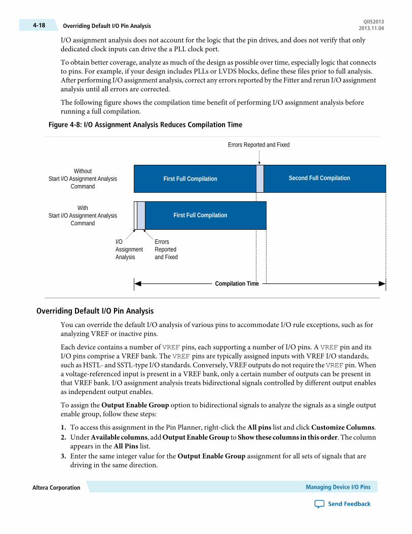
The following figure shows the compilation time benefit of performing I/O assignment analysis beforerunning a full compilation.
Figure 4-8: I/O Assignment Analysis Reduces Compilation Time
ErrorsReportedand Fixed
I/OAssignmentAnalysis
First Full Compilation
First Full Compilation
Second Full Compilation
Errors Reported and Fixed
WithoutStart I/O Assignment Analysis
Command
WithStart I/O Assignment Analysis
Command
Compilation Time
Overriding Default I/O Pin Analysis
You can override the default I/O analysis of various pins to accommodate I/O rule exceptions, such as foranalyzing VREF or inactive pins.
Each device contains a number of VREF pins, each supporting a number of I/O pins. A VREF pin and itsI/O pins comprise a VREF bank. The VREF pins are typically assigned inputs with VREF I/O standards,such asHSTL- and SSTL-type I/O standards. Conversely, VREF outputs do not require theVREF pin.Whena voltage-referenced input is present in a VREF bank, only a certain number of outputs can be present inthat VREF bank. I/O assignment analysis treats bidirectional signals controlled by different output enablesas independent output enables.
To assign the Output Enable Group option to bidirectional signals to analyze the signals as a single outputenable group, follow these steps:
1. To access this assignment in the Pin Planner, right-click the All pins list and click Customize Columns.2. UnderAvailable columns, addOutputEnableGroup to Show these columns in this order. The column
appears in the All Pins list.3. Enter the same integer value for the Output Enable Group assignment for all sets of signals that are
driving in the same direction.
Managing Device I/O PinsAltera Corporation
Send Feedback
QII52013Overriding Default I/O Pin Analysis4-18 2013.11.04

This assignment is especially important for external memory interfaces. For example, consider a DDR2interface in a Stratix II device. The device allows 30 pins in a VREF group. Each byte lane for a ×8 DDR2interface includes one DQS pin and eight DQ pins, for a total of nine pins per byte lane. The DDR2 interfaceuses the SSTL 18 Class I VREF I/O standard. In typical interfaces, each byte lane has its own output enable.In this example, the DDR2 interface has four byte lanes. Using 30 I/O pins in a VREF group, there are threebyte lanes and an extra byte lane that supports the three remaining pins. Without theOutput EnableGroupassignment, the Fitter analyzes each byte lane as an independent group driven by a unique output enable.In this worst-case scenario the three pins are inputs, and the other 27 pins are outputs violating the 20 outputpin limit.
Because DDR2 DQS and DQ pins are always driven in the same direction, the analysis reports an error thatis not applicable to your design. The Output Enable Group assignment designates the DQS and DQ pinsas a single group driven by a common output enable for I/O assignment analysis. When you use the OutputEnable Group logic option assignment, the DQS and DQ pins are checked as all input pins or all outputpins and are not in violation of the I/O rules.
You can also use the Output Enable Group assignment to designate pins that are driven only at certaintimes. For example, the data mask signal in DDR2 interfaces is an output signal, but it is driven only whenthe DDR2 is writing (bidirectional signals are outputs). To avoid I/O assignment analysis errors, use theOutput Enable Group logic option assignment to assign the data mask to the same value as the DQ andDQS signals.
You can also use the Output Enable Group to designate VREF input pins that are inactive during the timethe outputs are driving. This assignment removes theVREF input pins from theVREF analysis. For example,the QVLD signal for an RLDRAM II interface is active only during a read. During a write, the QVLD pin isnot active and does not count as an active VREF input pin in the VREF group. Place the QVLD pins in thesame output enable group as the RLDRAM II data pins.
Related InformationThe TimeQuest Timing Analyzer
Understanding I/O Analysis ReportsThe detailed I/O assignment analysis reports include the affected pin name and a problem description. TheFitter section of the Compilation report contains information generated during I/O assignment analysis,including the following reports:
• I/O Assignment Warnings—lists warnings generated for each pin• Resource Section—quantifies use of various pin types and I/O banks• I/O Rules Section—lists summary, details, and matrix information about the I/O rules tested
The Status column indicates whether rules passed, failed, or could not be checked. A severity rating indicatesthe rule’s importance for effective analysis. “Inapplicable” rules do not apply to the target device family.
Altera CorporationManaging Device I/O Pins
Send Feedback
4-19Understanding I/O Analysis ReportsQII520132013.11.04
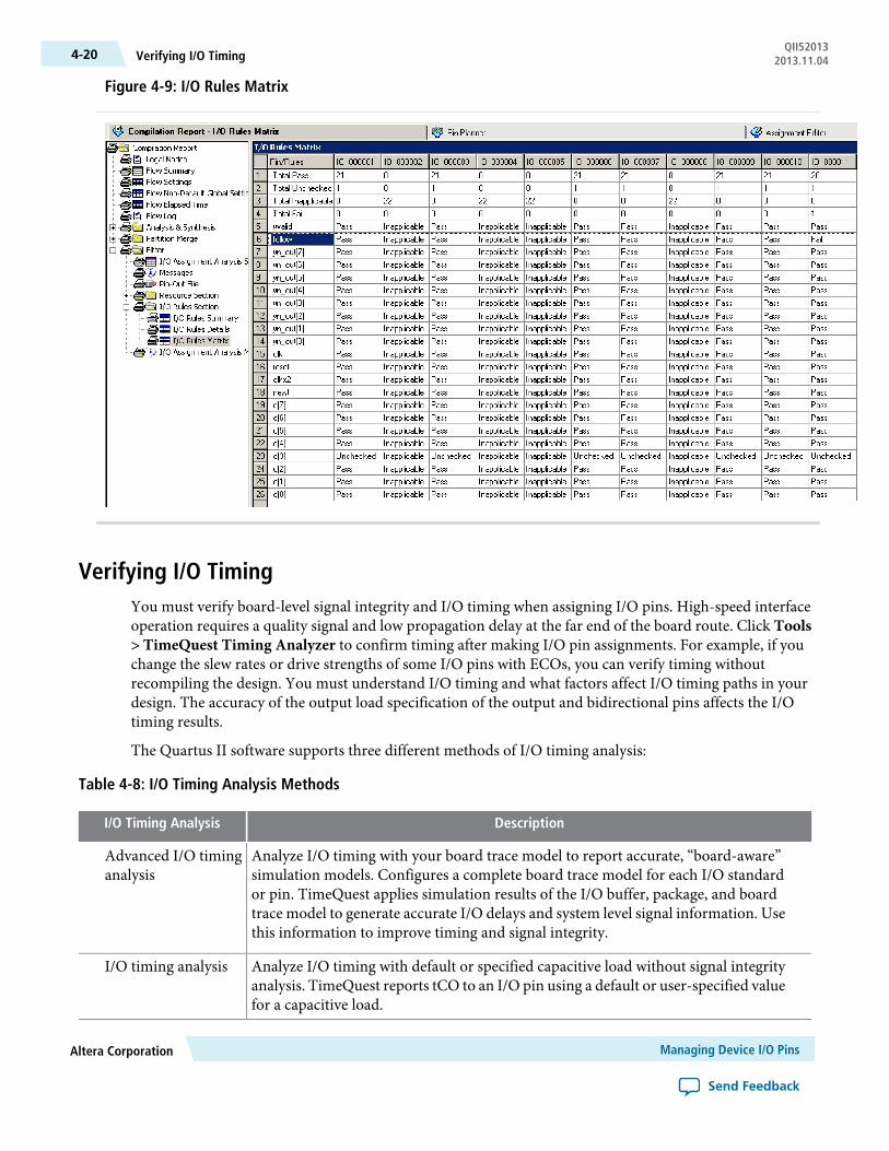
Figure 4-9: I/O Rules Matrix
Verifying I/O TimingYou must verify board-level signal integrity and I/O timing when assigning I/O pins. High-speed interfaceoperation requires a quality signal and low propagation delay at the far end of the board route. Click Tools> TimeQuest Timing Analyzer to confirm timing after making I/O pin assignments. For example, if youchange the slew rates or drive strengths of some I/O pins with ECOs, you can verify timing withoutrecompiling the design. You must understand I/O timing and what factors affect I/O timing paths in yourdesign. The accuracy of the output load specification of the output and bidirectional pins affects the I/Otiming results.
The Quartus II software supports three different methods of I/O timing analysis:
Table 4-8: I/O Timing Analysis Methods
DescriptionI/O Timing Analysis
Analyze I/O timing with your board trace model to report accurate, “board-aware”simulation models. Configures a complete board trace model for each I/O standardor pin. TimeQuest applies simulation results of the I/O buffer, package, and boardtrace model to generate accurate I/O delays and system level signal information. Usethis information to improve timing and signal integrity.
Advanced I/O timinganalysis
Analyze I/O timing with default or specified capacitive load without signal integrityanalysis. TimeQuest reports tCO to an I/O pin using a default or user-specified valuefor a capacitive load.
I/O timing analysis
Managing Device I/O PinsAltera Corporation
Send Feedback
QII52013Verifying I/O Timing4-20 2013.11.04
DescriptionI/O Timing Analysis
Use Altera-provided or Quartus II software-generated IBIS or HSPICE I/O modelsfor simulation in Mentor Graphics HyperLynx and Synopsys HSPICE.
Full board routingsimulation
Advanced I/O timing analysis is supported only for .28nm and larger device families. For devicesthat support advanced I/O timing, it is the defaultmethod of I/O timing analysis. For all other devices,
Note:
you must use a default or user-specified capacitive load assignment to determine tCO and powermeasurements.
For more information about advanced I/O timing support, refer to the appropriate device handbook foryour target device. For more information about board-level signal integrity and tips on how to improvesignal integrity in your high-speed designs, refer to the Altera Signal Integrity Center page of the Alterawebsite.
For information about creating IBIS and HSPICE models with the Quartus II software and integrating thosemodels into HyperLynx and HSPICE simulations, refer to theSignal Integrity Analysis with Third Party Toolschapter in volume 2 of the Quartus II Handbook.
Related Information
• Literature and Technical Documentation
• Altera Signal Integrity Center
• Signal Integrity Analysis with Third-Party Tools
Running Advanced I/O TimingAdvanced I/O timing analysis uses your board trace model and termination network specification to reportaccurate output buffer-to-pin timing estimates, FPGA pin and board trace signal integrity and delay values.Advanced I/O timing runs automatically for supported devices during compilation.
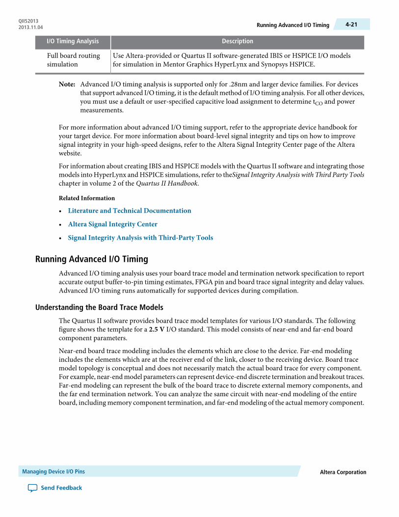
Understanding the Board Trace Models
The Quartus II software provides board trace model templates for various I/O standards. The followingfigure shows the template for a 2.5 V I/O standard. This model consists of near-end and far-end boardcomponent parameters.
Near-end board trace modeling includes the elements which are close to the device. Far-end modelingincludes the elements which are at the receiver end of the link, closer to the receiving device. Board tracemodel topology is conceptual and does not necessarily match the actual board trace for every component.For example, near-endmodel parameters can represent device-end discrete termination and breakout traces.Far-end modeling can represent the bulk of the board trace to discrete external memory components, andthe far end termination network. You can analyze the same circuit with near-end modeling of the entireboard, including memory component termination, and far-end modeling of the actual memory component.
Altera CorporationManaging Device I/O Pins
Send Feedback
4-21Running Advanced I/O TimingQII520132013.11.04
Figure 4-10: 2.5-V I/O Standard Board Trace Model
The following figure shows the template for the LVDS I/O standard. The far-end capacitance (Cf) representsthe external-device or multiple-device capacitive load. If you have multiple devices on the far-end, you mustfind the equivalent capacitance at the far-end, taking into account all receiver capacitances. The far-endcapacitance can be the sum of all the receiver capacitances.
TheQuartus II softwaremodels lossless transmission lines, and does not require a transmission-line resistancevalue. Only distributed inductance (L) and capacitance (C) values are needed. The distributed L andC valuesof transmission lines must be entered on a per-inch basis, and can be obtained from the PCB vendor ormanufacturer, the CAD Design tool, or a signal integrity tool, such as the Mentor Graphics Hyperlynxsoftware.
Managing Device I/O PinsAltera Corporation
Send Feedback
QII52013Understanding the Board Trace Models4-22 2013.11.04
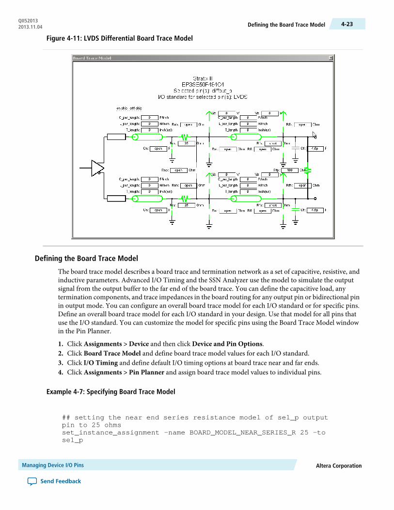
Figure 4-11: LVDS Differential Board Trace Model
Defining the Board Trace Model
The board trace model describes a board trace and termination network as a set of capacitive, resistive, andinductive parameters. Advanced I/O Timing and the SSN Analyzer use the model to simulate the outputsignal from the output buffer to the far end of the board trace. You can define the capacitive load, anytermination components, and trace impedances in the board routing for any output pin or bidirectional pinin output mode. You can configure an overall board trace model for each I/O standard or for specific pins.Define an overall board trace model for each I/O standard in your design. Use that model for all pins thatuse the I/O standard. You can customize the model for specific pins using the Board Trace Model windowin the Pin Planner.
1. Click Assignments > Device and then click Device and Pin Options.2. Click Board Trace Model and define board trace model values for each I/O standard.3. Click I/O Timing and define default I/O timing options at board trace near and far ends.4. Click Assignments > Pin Planner and assign board trace model values to individual pins.
Example 4-7: Specifying Board Trace Model
## setting the near end series resistance model of sel_p output pin to 25 ohmsset_instance_assignment -name BOARD_MODEL_NEAR_SERIES_R 25 -to se1_p
Altera CorporationManaging Device I/O Pins
Send Feedback
4-23Defining the Board Trace ModelQII520132013.11.04
## Setting the far end capacitance model for sel_p output signal to 6 picofaradsset_instance_assignment -name BOARD_MODEL_FAR_C 6P -to se1_p
Related Information
• Using Advanced I/O Timing
• Board Trace Models
Modifying the Board Trace Model
To modify the board trace model, click View > Board TraceModel in the Pin Planner. You can modify anyof the board trace model parameters within a graphical representation of the board trace model.
The Board Trace Model window displays the routing and components for positive and negative signals ina differential signal pair. Only modify the positive signal of the pair, as the setting automatically applies tothe negative signal. Use standard unit prefixes such as p, n, and k to represent pico, nano, and kilo, respectively.Use the short or open value to designate a short or open circuit for a parallel component.
Specifying Near-End vs Far-End I/O Timing Analysis
You can select a near-end or far-end point for I/O timing analysis. Near-end timing analysis extends to thedevice pin. You can apply the set_output_delay constraint during near end analysis to account forthe delay across the board.
Far-end I/O timing analysis, then advanced I/O timing analysis extends to the external device input, at thefar end of the board trace. Whether you choose a near-end or far-end timing endpoint, the board tracemodels are taken into account during timing analysis.
Understanding Advanced I/O Timing Analysis Reports
View I/O timing analysis information in the following reports:
Table 4-9: Advanced I/O Timing Reports
DescriptionI/O Timing Report
Reports signal integrity and board delay data.TimeQuest Report
Summarizes the board trace model component settings for each output andbidirectional signal.
Board Trace ModelAssignments report
Contains all the signal integrity metrics calculated during advanced I/O timinganalysis based on the board tracemodel settings for each output or bidirectionalpin. Includes measurements at both the FPGA pin and at the far-end load ofboard delay, steady state voltages, and rise and fall times.
Signal Integrity Metricsreport
By default, the TimeQuest analyzer generates the Slow-Corner Signal Integrity Metrics report. Togenerate a Fast-Corner Signal Integrity Metrics report you must change the delay model by clickingTools > TimeQuest Timing Analyzer.
Note:
Managing Device I/O PinsAltera Corporation
Send Feedback
QII52013Modifying the Board Trace Model4-24 2013.11.04
Related InformationThe TimeQuest Timing Analyzer
Adjusting I/O Timing and Power with Capacitive LoadingWhen calculating tCO and power for output and bidirectional pins, the TimeQuest analyzer and the PowerPlayPower Analyzer use a bulk capacitive load. You can adjust the value of the capacitive load per I/O standardto obtain more precise tCO and power measurements, reflecting the behavior of the output or bidirectionalnet on your PCB. The Quartus II software ignores capacitive load settings on input pins. You can adjust thecapacitive load settings per I/O standard, in picofarads (pF), for your entire design. During compilation, theCompiler measures power and tCO measurements based on your settings. You can also adjust the capacitiveload on an individual pin with the Output Pin Load logic option.
Viewing Routing and Timing DelaysRight-click any node and click Locate > Locate in Chip Planner to visualize and adjust I/O timing delaysand routing between user I/O pads and VCC, GND, and VREF pads. The Chip Planner graphically displayslogic placement, LogicLock regions, relative resource usage, detailed routing information, fan-in and fan-out, register paths, and high-speed transceiver channels. You can view physical timing estimates, routingcongestion, and clock regions. Use the Chip Planner to change connections between resources and makepost-compilation changes to logic cell and I/O atom placement. When you select items in the Pin Planner,the corresponding item is highlighted in Chip Planner.
Analyzing Simultaneous Switching NoiseClick Processing > Start > Start SSN Analyzer to estimate the voltage noise for each pin in the design. Thesimultaneous switching noise (SSN) analysis accounts for the pin placement, I/O standard, board trace,output enable group, timing constraint, and PCB characteristics that you specify. The analysis produces avoltage noise estimate for each pin in the design. View the SSN results in the Pin Planner and adjust yourI/O assignments to optimize signal integrity.
Related InformationSimultaneous Switching Noise (SSN) Analysis and Optimization
Scripting APIYou can alternatively use Tcl commands to access I/O management functions, rather than using the GUI.For detailed information about specific scripting command options and Tcl API packages, type the followingcommand at a system command prompt to view the Tcl API Help browser:
quartus_sh --qhelp
Related Information
• Tcl Scripting
• Command Line Scripting
Altera CorporationManaging Device I/O Pins
Send Feedback
4-25Adjusting I/O Timing and Power with Capacitive LoadingQII520132013.11.04

Run I/O Assignment AnalysisEnter the following in the Tcl console or a Tcl script:
execute_flow -check_ios
Type the following at a system command prompt:
quartus_fit <project name> --check_ios
Generate Mapped NetlistEnter the following in the Tcl console or in a Tcl script:
execute_module -tool map
The execute_module command is in the flow package.
Type the following at a system command prompt:
quartus_map <project name>
Reserve PinsUse the following Tcl command to reserve a pin:
set_instance_assignment -name RESERVE_PIN <value> -to <signal name>
Use one of the following valid reserved pin values:
• "AS BIDIRECTIONAL"
• "AS INPUT TRI STATED"
• "AS OUTPUT DRIVING AN UNSPECIFIED SIGNAL"
• "AS OUTPUT DRIVING GROUND"
• "AS SIGNALPROBE OUTPUT"
You must include the quotation marks when specifying the reserved pin value.Note:
Set LocationUse the following Tcl command to assign a signal to a pin or device location:
set_location_assignment <location> -to <signal name>
Valid locations are pin locations, I/O bank locations, or edge locations. Pin locations include pin names,such as PIN_A3. I/O bank locations include IOBANK_1 up to IOBANK_ n, where n is the number of I/Obanks in the device.
Managing Device I/O PinsAltera Corporation
Send Feedback
QII52013Run I/O Assignment Analysis4-26 2013.11.04
Use one of the following valid edge location values:
• EDGE_BOTTOM
• EDGE_LEFT
• EDGE_TOP
• EDGE_RIGHT
Exclusive I/O GroupUse the following Tcl command to create an exclusive I/O group assignments:
set_instance_assignment -name "EXCLUSIVE_IO_GROUP" -to pin
Slew Rate and Current StrengthUse the following Tcl commands to create an slew rate and drive strength assignments:
set_instance_assignment -name CURRENT_STRENGTH_NEW 8MA -to e[0]set_instance_assignment -name SLEW_RATE 2 -to e[0]
Related InformationAltera Device Package Information Data Sheet
Document Revision HistoryThe following table shows the revision history for this chapter.
Table 4-10: Document Revision History
ChangesVersionDate
• Reorganization and conversion to DITA.13.1.0November 2013
• Added information about overriding I/O placement rules.13.0.0May 2013
• Updated Pin Planner description for new task and report windows.12.1.0November 2012
• Removed survey link.12.0.0June 2012
• Minor updates and corrections.• Updated the document template.
11.1.0November 2011
Template update10.0.1December 2010
Altera CorporationManaging Device I/O Pins
Send Feedback
4-27Exclusive I/O GroupQII520132013.11.04
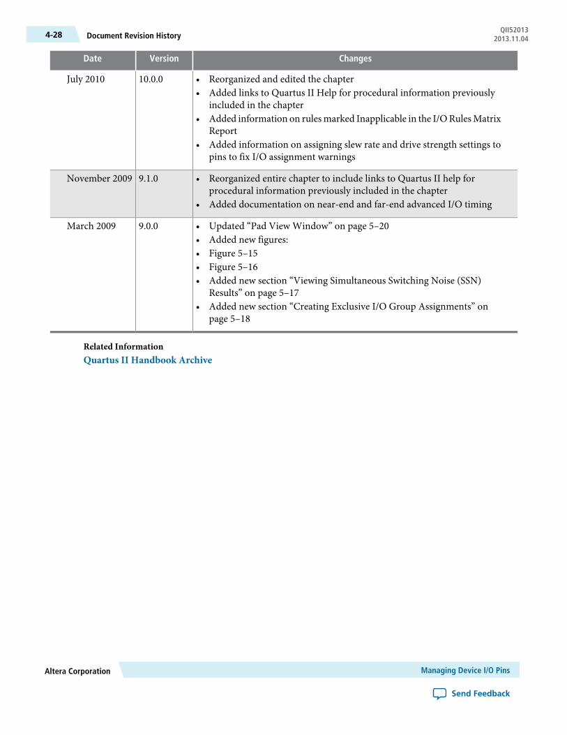
ChangesVersionDate
• Reorganized and edited the chapter• Added links to Quartus II Help for procedural information previously
included in the chapter• Added information on rulesmarked Inapplicable in the I/ORulesMatrix
Report• Added information on assigning slew rate and drive strength settings to
pins to fix I/O assignment warnings
10.0.0July 2010
• Reorganized entire chapter to include links to Quartus II help forprocedural information previously included in the chapter
• Added documentation on near-end and far-end advanced I/O timing
9.1.0November 2009
• Updated “Pad View Window” on page 5–20• Added new figures:• Figure 5–15• Figure 5–16• Added new section “Viewing Simultaneous Switching Noise (SSN)
Results” on page 5–17• Added new section “Creating Exclusive I/O Group Assignments” on
page 5–18
9.0.0March 2009
Related InformationQuartus II Handbook Archive
Managing Device I/O PinsAltera Corporation
Send Feedback
QII52013Document Revision History4-28 2013.11.04