maharashtra state board of technical education (autonomous...
TRANSCRIPT

MAHARASHTRA STATE BOARD OF TECHNICAL EDUCATION
(Autonomous)
(ISO/IEC - 27001 - 2005 Certified)
_________________________________________________________________________
Page 1 of 26
Summer 2015 Examination
Subject Code: 17213 Model Answer
Important Instructions to examiners:
1) The answers should be examined by key words and not as word-to-word as given in the
model answer scheme.
2) The model answer and the answer written by candidate may vary but the examiner may try
to assess the understanding level of the candidate.
3) The language errors such as grammatical, spelling errors should not be given more
Importance (Not applicable for subject English and Communication Skills).
4) While assessing figures, examiner may give credit for principal components indicated in
the figure. The figures drawn by candidate and model answer may vary. The examiner may
give credit for any equivalent figure drawn.
5) Credits may be given step wise for numerical problems. In some cases, the assumed
constant values may vary and there may be some difference in the candidate’s answers and
model answer.
6) In case of some questions credit may be given by judgement on part of examiner of
relevant answer based on candidate’s understanding.
7) For programming language papers, credit may be given to any other program based on
equivalent concept.
MAHARASHTRA STATE BOARD OF TECHNICAL EDUCATION
(Autonomous)
(ISO/IEC - 27001 - 2005 Certified)
_________________________________________________________________________
Page 2 of 26
1. Attempt any TEN: 20
a. Define passive component. Give its examples
Ans a. Definition: 1 M; Examples: 1M
Passive components: the Passive components is one which does not introduce any gain
Eg: Resistor, Capacitor, and Inductor.
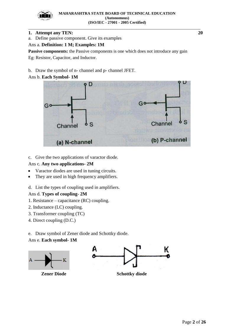
b. Draw the symbol of n- channel and p- channel JFET.
Ans b. Each Symbol- 1M
c. Give the two applications of varactor diode.
Ans c. Any two applications- 2M
Varactor diodes are used in tuning circuits.
They are used in high frequency amplifiers.
d. List the types of coupling used in amplifiers.
Ans d. Types of coupling- 2M
1. Resistance – capacitance (RC) coupling.
2. Inductance (LC) coupling.
3. Transformer coupling (TC)
4. Direct coupling (D.C.)
e. Draw symbol of Zener diode and Schottky diode.
Ans e. Each symbol- 1M
Zener Diode Schottky diode

MAHARASHTRA STATE BOARD OF TECHNICAL EDUCATION
(Autonomous)
(ISO/IEC - 27001 - 2005 Certified)
_________________________________________________________________________
Page 3 of 26
f. Give two advantages and two disadvantages of IC’s
Ans f. Two advantages: 1M; Disadvantages: 1M
Advantages of IC’s are:
1. The physical size of an IC is extremely small (generally thousand times smaller) than that
of discrete circuits.
2. The weight of an IC is very less as compared to that of equivalent discrete circuits.
3. The reduction in power consumption is achieved due to extremely small size of IC.
4. Interconnection errors are non-existent in practice.
5. Temperature differences between components of a circuit are small.
6. Close matching of components and temperature coefficients is possible.
7. In case of circuit failure, it is very easy to replace an IC by a new one.
8. Active devices can be generously used as they are cheaper than passive components.
Disadvantages of IC’s are:
1. It is not possible to directly fabricate inductors.
2. The initial cost to be incurred is high
3. Power dissipation is limited.
4. ICs are very delicate and need extra care while handling.
g. List the types of filter.
Ans g. Types of filter:2 M
Filters are classified depending on the components used and depending on the configuration
in which they are connected.
Some of the important types are as follows:
1. Capacitor input filter (shunt capacitor filter)
2. Choke input filter (series inductor filter)
3. LC filter
4. π type filter OR CLC filter
5. RC filter.
h. Define the following FET parameters:
Amplification factor.- 1M
Transconductance-1M
Transconductance
Transconductance is defined as the ratio of change in Drain current (ΔID) to change in Gate to
Source Voltage (ΔVGS) at a constant VDS.
Amplification Factor
Amplification Factor is defined as the ratio of change in Drain to Source Voltage (ΔVDS) to
change in Gate to Source Voltage (ΔVGS) at a constant ID.
MAHARASHTRA STATE BOARD OF TECHNICAL EDUCATION
(Autonomous)
(ISO/IEC - 27001 - 2005 Certified)
_________________________________________________________________________
Page 4 of 26
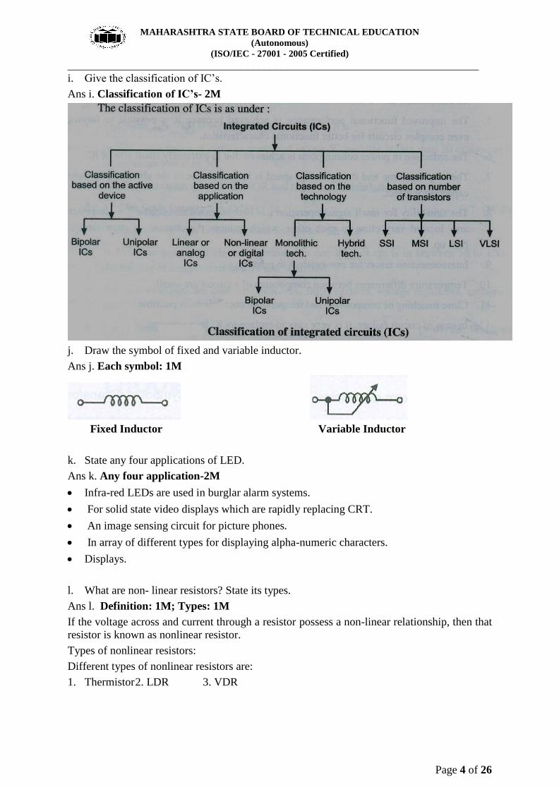
i. Give the classification of IC’s.
Ans i. Classification of IC’s- 2M
j. Draw the symbol of fixed and variable inductor.
Ans j. Each symbol: 1M
Fixed Inductor Variable Inductor
k. State any four applications of LED.
Ans k. Any four application-2M
Infra-red LEDs are used in burglar alarm systems.
For solid state video displays which are rapidly replacing CRT.
An image sensing circuit for picture phones.
In array of different types for displaying alpha-numeric characters.
Displays.
l. What are non- linear resistors? State its types.
Ans l. Definition: 1M; Types: 1M
If the voltage across and current through a resistor possess a non-linear relationship, then that
resistor is known as nonlinear resistor.
Types of nonlinear resistors:
Different types of nonlinear resistors are:
1. Thermistor 2. LDR 3. VDR
MAHARASHTRA STATE BOARD OF TECHNICAL EDUCATION
(Autonomous)
(ISO/IEC - 27001 - 2005 Certified)
_________________________________________________________________________
Page 5 of 26
2. Attempt any FOUR: 16
a. State any four applications of electronics
Ans a. Any four applications: 4M
1. Communication and Entertainment:
a) Wire communication or Line communication.
b) Wireless communication.
The examples of wire communication are Telegraphy, Telephony, Telex and Teleprinter. The
examples of wireless communication are radio broadcasting, TV broadcasting, and satellite
communication.
2. Defense: The most important application is RADAR.
3. Industrial Applications: Electronic circuits are used to control thickness, quality, weight
and moisture. They are also used to amplify weak signals.
4. Medical sciences: Electronics helps doctors and scientists in the diagnosis and treatment of
various diseases. E.g. X-rays, ECG, Oscillographs and Short-wave diathermy units.
5. Instrumentation: Instrumentation plays very vital role in research field and industry. E.g.
Cathode Ray Oscilloscope (CRO), Frequency counter, Signal generator and Strain gauges.
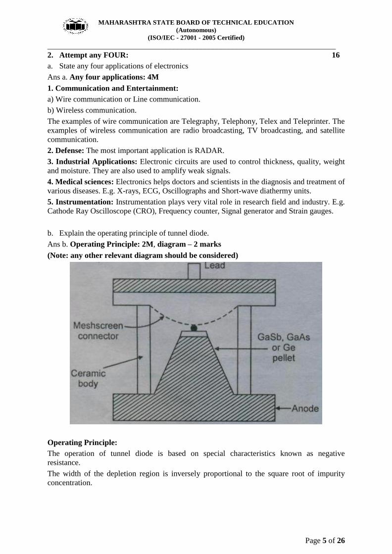
b. Explain the operating principle of tunnel diode.
Ans b. Operating Principle: 2M, diagram – 2 marks
(Note: any other relevant diagram should be considered)
Operating Principle:
The operation of tunnel diode is based on special characteristics known as negative
resistance.
The width of the depletion region is inversely proportional to the square root of impurity
concentration.
MAHARASHTRA STATE BOARD OF TECHNICAL EDUCATION
(Autonomous)
(ISO/IEC - 27001 - 2005 Certified)
_________________________________________________________________________
Page 6 of 26
So increase in the impurity concentration, the depletion region width will reduce. The
thickness of depletion region of this diode is so small. That indicates there is large probability
of an electron can penetrate through this barrier.
This behavior is called is tunneling & hence the name of the high impurity density PN
junction is called as tunnel diode.
An ordinary PN junction diode has an impurity concentration of about 1 part in 108 and its
depletion region width is of the order 5 microns. If the concentration of impurity is increased
to about 1 part in 103, the device characteristics are completely changed. Due to the thin
potential energy barrier, the electrons penetrate through the junction rather than surmounting
them. This quantum mechanical behavior is referred to as tunneling and these high impurity
density PN junction devices are called tunnel diodes.
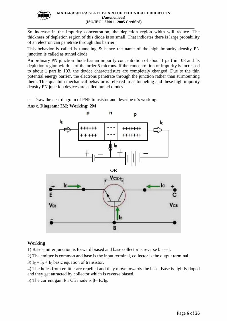
c. Draw the neat diagram of PNP transistor and describe it’s working.
Ans c. Diagram: 2M; Working: 2M
OR
Working
1) Base emitter junction is forward biased and base collector is reverse biased.
2) The emitter is common and base is the input terminal, collector is the output terminal.
3) IE = IB + IC basic equation of transistor.
4) The holes from emitter are repelled and they move towards the base. Base is lightly doped
and they get attracted by collector which is reverse biased.
5) The current gain for CE mode is β= Ic/IB.

MAHARASHTRA STATE BOARD OF TECHNICAL EDUCATION
(Autonomous)
(ISO/IEC - 27001 - 2005 Certified)
_________________________________________________________________________
Page 7 of 26
d. Distinguish between PN junction diode and zener diode.
Ans d. any Four Points: 4 M
Sr.No. PN Junction Diode
Zener Diode
1 It is not properly doped to control reverse
breakdown.
It is properly doped to control reverse
breakdown.
2 It conducts only in one direction.
It conducts in both directions.
3 It is always operated in forward-bias
condition.
It is always operated in reverse-bias
condition.
4 It has no sharp reverse breakdown.
It has quite sharp reverse breakdown.
5 It burns immediately, if applied voltage
exceeds the breakdown voltage.
It will not burn, but functions properly in
breakdown region.
6 It is commonly used for rectification
purpose.
It cannot be used for rectification, but
commonly used for voltage regulation.
e. Define oscillator. State its need and condition required for sustained oscillations.
Ans e. Define: 2M; Need: 1M; Condition: 1M
(Note: Any relevant correct definition should be considered)
The electronic oscillator is a voltage amplifier with a LC tank circuit as a collector load
having a positive feedback and generating the undamped oscillations across the road.
(OR)
An oscillator is a electronic circuit that produces a periodic waveform on its output with only
dc supply voltage as an input.
Need of Oscillators:
The AC generating machine i.e. alternator can generate frequencies up to 1 kHz.
It is not possible to generate very high frequencies with the alternator due to its limitations.
Therefore, electronic oscillators are necessary.
Barkhausen Criterion for Oscillations
1. Loop gain (β.Av) ≥ 1
2. Phase shift between the input and output signal must be equal to 3600 or 00.
MAHARASHTRA STATE BOARD OF TECHNICAL EDUCATION
(Autonomous)
(ISO/IEC - 27001 - 2005 Certified)
_________________________________________________________________________
Page 8 of 26
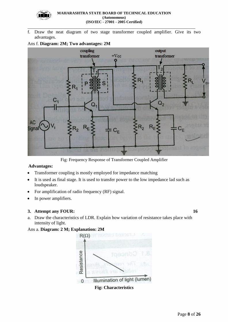
f. Draw the neat diagram of two stage transformer coupled amplifier. Give its two
advantages.
Ans f. Diagram: 2M; Two advantages: 2M
Fig: Frequency Response of Transformer Coupled Amplifier
Advantages:
Transformer coupling is mostly employed for impedance matching
It is used as final stage. It is used to transfer power to the low impedance lad such as
loudspeaker.
For amplification of radio frequency (RF) signal.
In power amplifiers.
3. Attempt any FOUR: 16
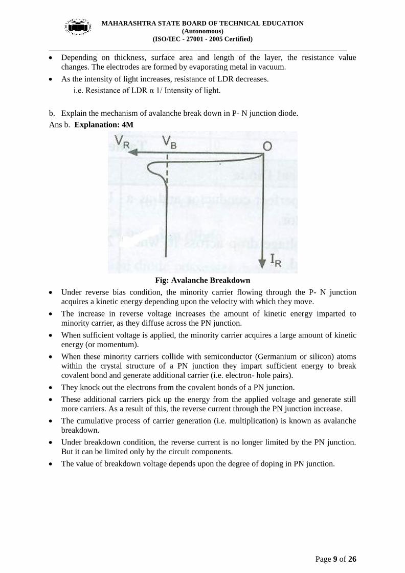
a. Draw the characteristics of LDR. Explain how variation of resistance takes place with
intensity of light.
Ans a. Diagram: 2 M; Explanation: 2M
Fig: Characteristics
MAHARASHTRA STATE BOARD OF TECHNICAL EDUCATION
(Autonomous)
(ISO/IEC - 27001 - 2005 Certified)
_________________________________________________________________________
Page 9 of 26
Depending on thickness, surface area and length of the layer, the resistance value
changes. The electrodes are formed by evaporating metal in vacuum.
As the intensity of light increases, resistance of LDR decreases.
i.e. Resistance of LDR α 1/ Intensity of light.
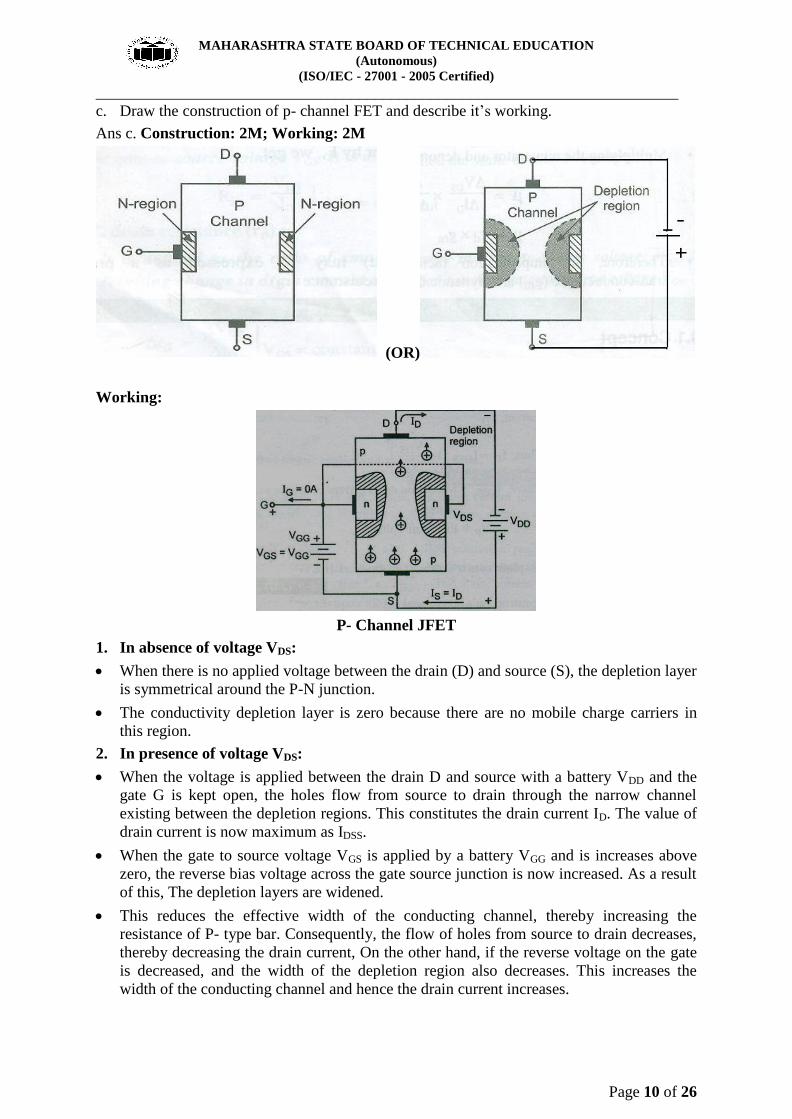
b. Explain the mechanism of avalanche break down in P- N junction diode.
Ans b. Explanation: 4M
Fig: Avalanche Breakdown
Under reverse bias condition, the minority carrier flowing through the P- N junction
acquires a kinetic energy depending upon the velocity with which they move.
The increase in reverse voltage increases the amount of kinetic energy imparted to
minority carrier, as they diffuse across the PN junction.
When sufficient voltage is applied, the minority carrier acquires a large amount of kinetic
energy (or momentum).
When these minority carriers collide with semiconductor (Germanium or silicon) atoms
within the crystal structure of a PN junction they impart sufficient energy to break
covalent bond and generate additional carrier (i.e. electron- hole pairs).
They knock out the electrons from the covalent bonds of a PN junction.
These additional carriers pick up the energy from the applied voltage and generate still
more carriers. As a result of this, the reverse current through the PN junction increase.
The cumulative process of carrier generation (i.e. multiplication) is known as avalanche
breakdown.
Under breakdown condition, the reverse current is no longer limited by the PN junction.
But it can be limited only by the circuit components.
The value of breakdown voltage depends upon the degree of doping in PN junction.
MAHARASHTRA STATE BOARD OF TECHNICAL EDUCATION
(Autonomous)
(ISO/IEC - 27001 - 2005 Certified)
_________________________________________________________________________
Page 10 of 26
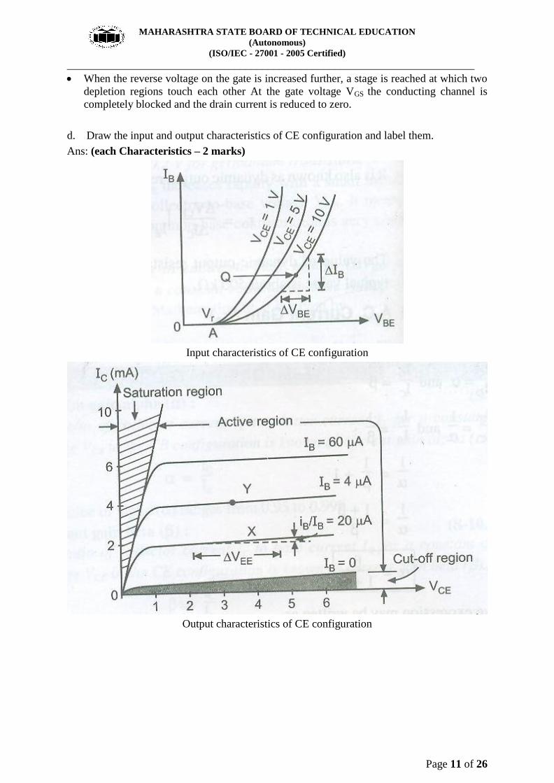
c. Draw the construction of p- channel FET and describe it’s working.
Ans c. Construction: 2M; Working: 2M
(OR)
Working:
P- Channel JFET
1. In absence of voltage VDS:
When there is no applied voltage between the drain (D) and source (S), the depletion layer
is symmetrical around the P-N junction.
The conductivity depletion layer is zero because there are no mobile charge carriers in
this region.
2. In presence of voltage VDS:
When the voltage is applied between the drain D and source with a battery VDD and the
gate G is kept open, the holes flow from source to drain through the narrow channel
existing between the depletion regions. This constitutes the drain current ID. The value of
drain current is now maximum as IDSS.
When the gate to source voltage VGS is applied by a battery VGG and is increases above
zero, the reverse bias voltage across the gate source junction is now increased. As a result
of this, The depletion layers are widened.
This reduces the effective width of the conducting channel, thereby increasing the
resistance of P- type bar. Consequently, the flow of holes from source to drain decreases,
thereby decreasing the drain current, On the other hand, if the reverse voltage on the gate
is decreased, and the width of the depletion region also decreases. This increases the
width of the conducting channel and hence the drain current increases.
MAHARASHTRA STATE BOARD OF TECHNICAL EDUCATION
(Autonomous)
(ISO/IEC - 27001 - 2005 Certified)
_________________________________________________________________________
Page 11 of 26
When the reverse voltage on the gate is increased further, a stage is reached at which two
depletion regions touch each other At the gate voltage VGS the conducting channel is
completely blocked and the drain current is reduced to zero.
d. Draw the input and output characteristics of CE configuration and label them.
Ans: (each Characteristics – 2 marks)
Input characteristics of CE configuration
Output characteristics of CE configuration
MAHARASHTRA STATE BOARD OF TECHNICAL EDUCATION
(Autonomous)
(ISO/IEC - 27001 - 2005 Certified)
_________________________________________________________________________
Page 12 of 26
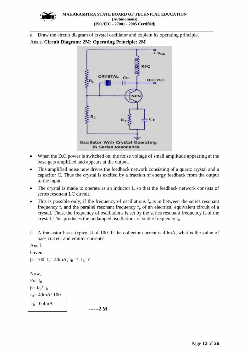
e. Draw the circuit diagram of crystal oscillator and explain its operating principle.
Ans e. Circuit Diagram: 2M; Operating Principle: 2M
When the D.C power is switched on, the noise voltage of small amplitude appearing at the
base gets amplified and appears at the output.
This amplified noise now drives the feedback network consisting of a quartz crystal and a
capacitor C. Thus the crystal is excited by a fraction of energy feedback from the output
to the input.
The crystal is made to operate as an inductor L so that the feedback network consists of
series resonant LC circuit.
This is possible only, if the frequency of oscillations fo is in between the series resonant
frequency fs and the parallel resonant frequency fp of an electrical equivalent circuit of a
crystal, Thus, the frequency of oscillations is set by the series resonant frequency fs of the
crystal. This produces the undamped oscillations of stable frequency fo.
f. A transistor has a typical β of 100. If the collector current is 40mA, what is the value of
base current and emitter current?
Ans f.
Given:
β= 100; Ic= 40mA; IB=?; IE=?
Now,
For IB
β= IC / IB
IB= 40mA/ 100
------2 M
IB= 0.4mA

MAHARASHTRA STATE BOARD OF TECHNICAL EDUCATION
(Autonomous)
(ISO/IEC - 27001 - 2005 Certified)
_________________________________________________________________________
Page 13 of 26
For,
IE= IB+ IB
= 0.4+ 400
------ 2M
4) Attempt any FOUR: 16
a. Draw the forward and reverse characteristics of PN junction diode and describe in brief.
Ans a. Diagram: 2 M; Description: 2M
The forward characteristic is the graph of the anode to cathode forward voltage VF
versus the forward current through the diode (IF).
The forward characteristics is divided into two portions, AB and BC
Region A to B of the forward characteristics.
The forward voltage is small and less than the cut in voltage. Therefore the forward
current flowing through the diode is small. With further increase in the forward
voltage, it reaches the level of the cut in voltage and the width the depletion region
goes on decreasing.
Region B to C:
As soon as the forward voltage equals the cut in voltage, current through the diode
increase suddenly. The nature of this current is exponential. The large forward current
in the region B-C of the forward characteristics is limited by connecting a resistor R in
series with the diode. Forward current is of the order of a few mA.
The forward current is a conventional current that flows from anode to cathode.
Therefore it is considered to be a positive current, and the forward characteristics
appears in the first quadrant.
Cut in voltage (Knee voltage):
The voltage at which the forward diode current starts increasing rapidly is known as
the cut in voltage of a diode. The cut in voltage is very close to the barrier potential.
Cut in voltage is also called as knee voltage.
Generally a diode is forward biased above the cut in voltage. The cut in voltage for a
silicon diode is 0.6 V and that for a germanium diode is 0.2V.
IE= 400.4mA
MAHARASHTRA STATE BOARD OF TECHNICAL EDUCATION
(Autonomous)
(ISO/IEC - 27001 - 2005 Certified)
_________________________________________________________________________
Page 14 of 26
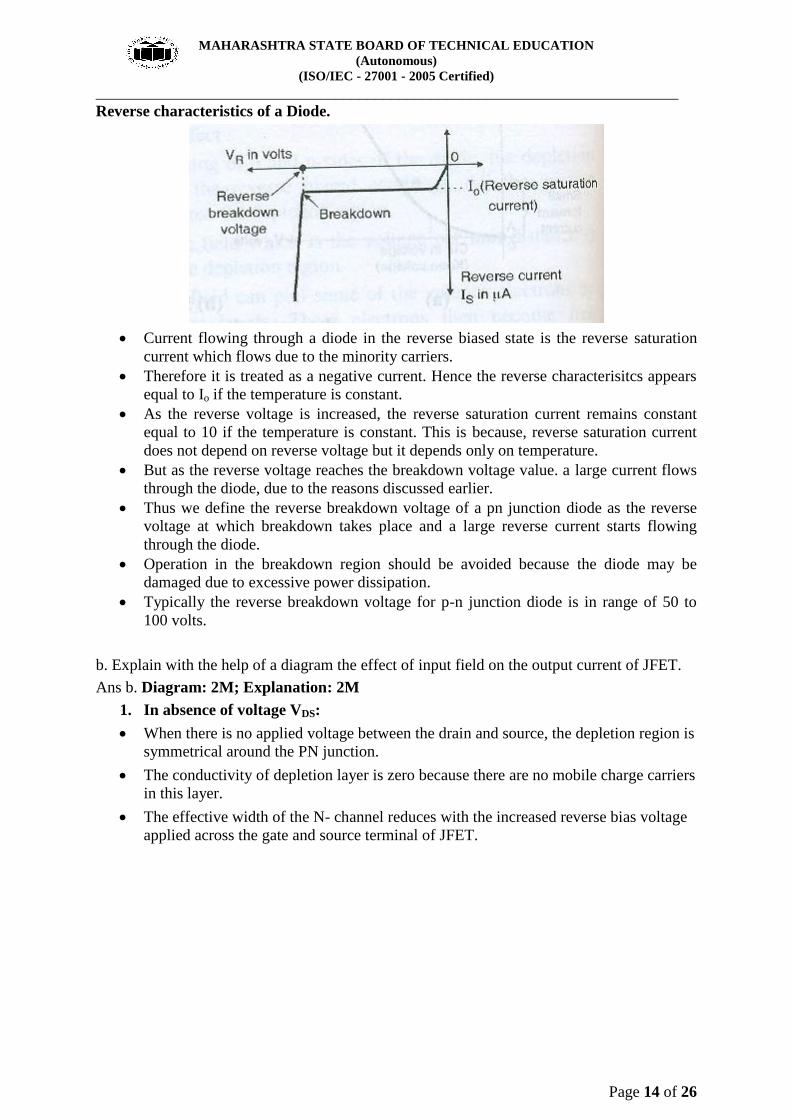
Reverse characteristics of a Diode.
Current flowing through a diode in the reverse biased state is the reverse saturation
current which flows due to the minority carriers.
Therefore it is treated as a negative current. Hence the reverse characterisitcs appears
equal to Io if the temperature is constant.
As the reverse voltage is increased, the reverse saturation current remains constant
equal to 10 if the temperature is constant. This is because, reverse saturation current
does not depend on reverse voltage but it depends only on temperature.
But as the reverse voltage reaches the breakdown voltage value. a large current flows
through the diode, due to the reasons discussed earlier.
Thus we define the reverse breakdown voltage of a pn junction diode as the reverse
voltage at which breakdown takes place and a large reverse current starts flowing
through the diode.
Operation in the breakdown region should be avoided because the diode may be
damaged due to excessive power dissipation.
Typically the reverse breakdown voltage for p-n junction diode is in range of 50 to
100 volts.
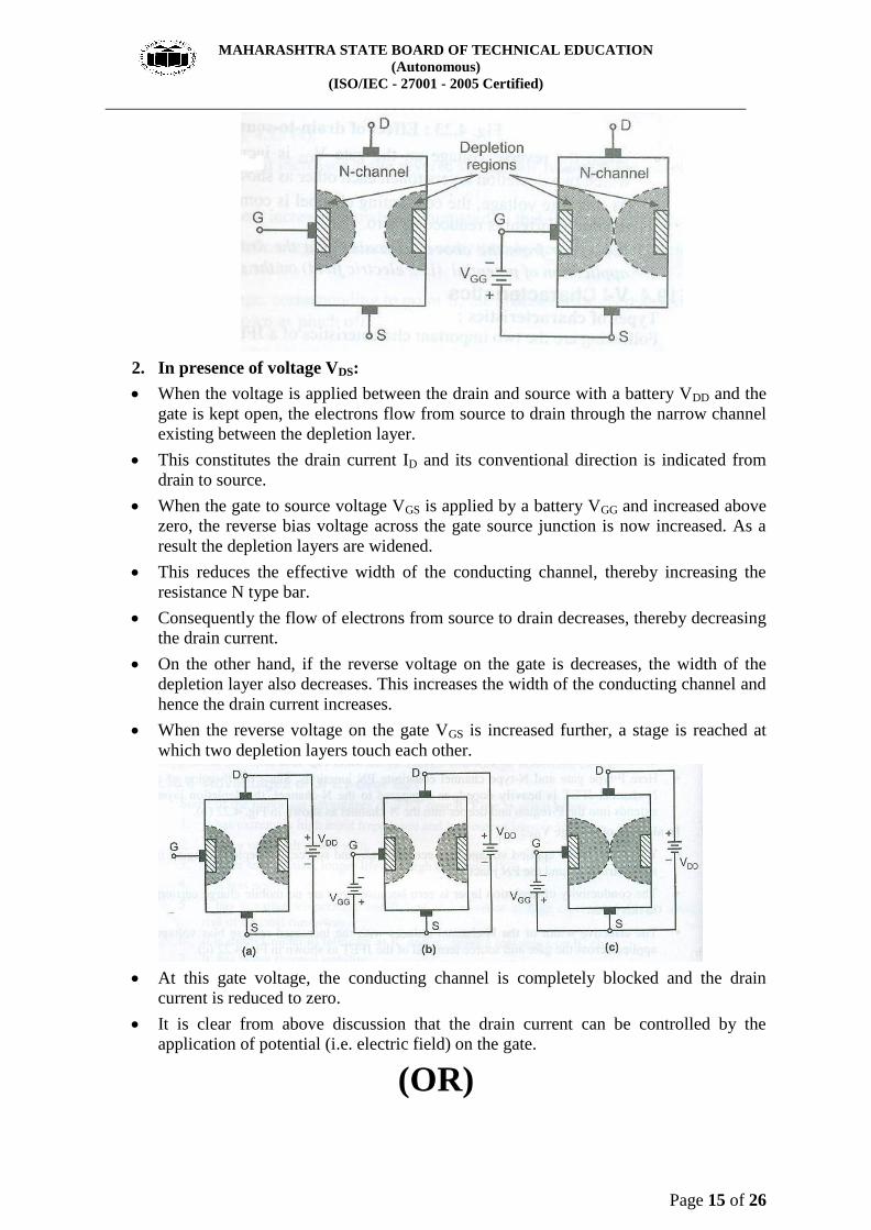
b. Explain with the help of a diagram the effect of input field on the output current of JFET.
Ans b. Diagram: 2M; Explanation: 2M
1. In absence of voltage VDS:
When there is no applied voltage between the drain and source, the depletion region is
symmetrical around the PN junction.
The conductivity of depletion layer is zero because there are no mobile charge carriers
in this layer.
The effective width of the N- channel reduces with the increased reverse bias voltage
applied across the gate and source terminal of JFET.
MAHARASHTRA STATE BOARD OF TECHNICAL EDUCATION
(Autonomous)
(ISO/IEC - 27001 - 2005 Certified)
_________________________________________________________________________
Page 15 of 26
2. In presence of voltage VDS:
When the voltage is applied between the drain and source with a battery VDD and the
gate is kept open, the electrons flow from source to drain through the narrow channel
existing between the depletion layer.
This constitutes the drain current ID and its conventional direction is indicated from
drain to source.
When the gate to source voltage VGS is applied by a battery VGG and increased above
zero, the reverse bias voltage across the gate source junction is now increased. As a
result the depletion layers are widened.
This reduces the effective width of the conducting channel, thereby increasing the
resistance N type bar.
Consequently the flow of electrons from source to drain decreases, thereby decreasing
the drain current.
On the other hand, if the reverse voltage on the gate is decreases, the width of the
depletion layer also decreases. This increases the width of the conducting channel and
hence the drain current increases.
When the reverse voltage on the gate VGS is increased further, a stage is reached at
which two depletion layers touch each other.
At this gate voltage, the conducting channel is completely blocked and the drain
current is reduced to zero.
It is clear from above discussion that the drain current can be controlled by the
application of potential (i.e. electric field) on the gate.
(OR)
MAHARASHTRA STATE BOARD OF TECHNICAL EDUCATION
(Autonomous)
(ISO/IEC - 27001 - 2005 Certified)
_________________________________________________________________________
Page 16 of 26
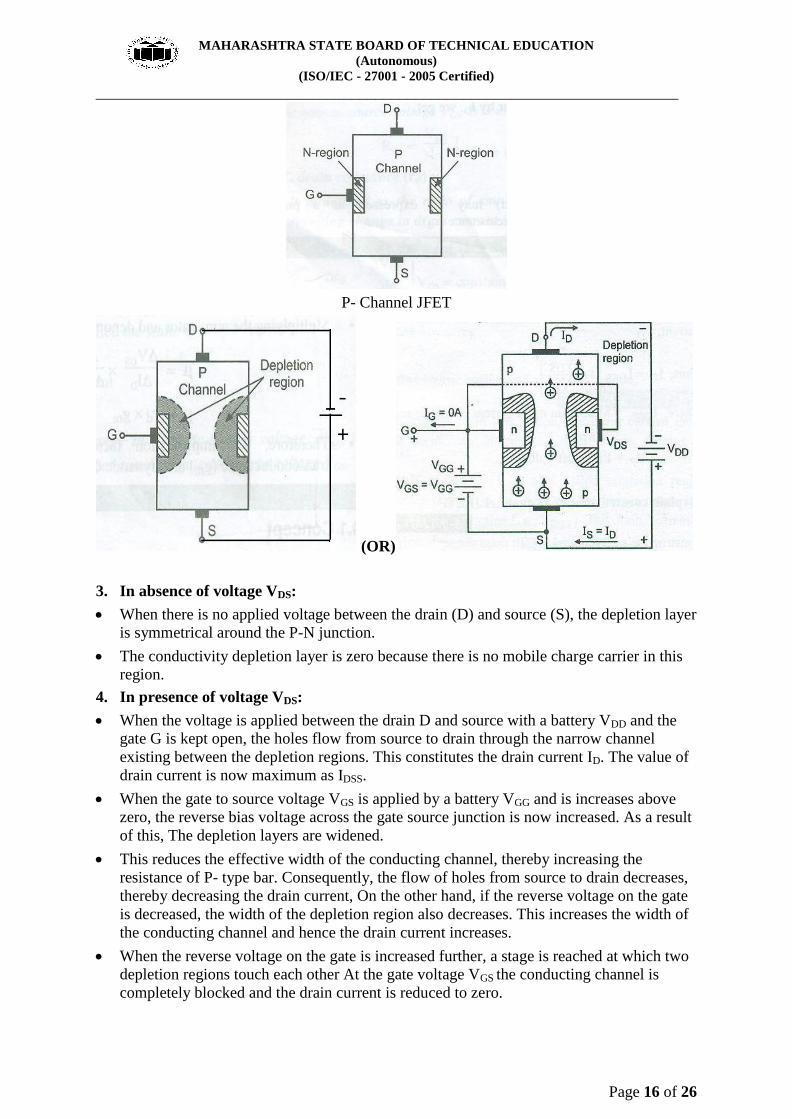
P- Channel JFET
(OR)
3. In absence of voltage VDS:
When there is no applied voltage between the drain (D) and source (S), the depletion layer
is symmetrical around the P-N junction.
The conductivity depletion layer is zero because there is no mobile charge carrier in this
region.
4. In presence of voltage VDS:
When the voltage is applied between the drain D and source with a battery VDD and the
gate G is kept open, the holes flow from source to drain through the narrow channel
existing between the depletion regions. This constitutes the drain current ID. The value of
drain current is now maximum as IDSS.
When the gate to source voltage VGS is applied by a battery VGG and is increases above
zero, the reverse bias voltage across the gate source junction is now increased. As a result
of this, The depletion layers are widened.
This reduces the effective width of the conducting channel, thereby increasing the
resistance of P- type bar. Consequently, the flow of holes from source to drain decreases,
thereby decreasing the drain current, On the other hand, if the reverse voltage on the gate
is decreased, the width of the depletion region also decreases. This increases the width of
the conducting channel and hence the drain current increases.
When the reverse voltage on the gate is increased further, a stage is reached at which two
depletion regions touch each other At the gate voltage VGS the conducting channel is
completely blocked and the drain current is reduced to zero.
MAHARASHTRA STATE BOARD OF TECHNICAL EDUCATION
(Autonomous)
(ISO/IEC - 27001 - 2005 Certified)
_________________________________________________________________________
Page 17 of 26
c. Differentiate between Half wave rectifier and bridge full wave rectifier (any four points)
Ans c. Any four points: 4 M
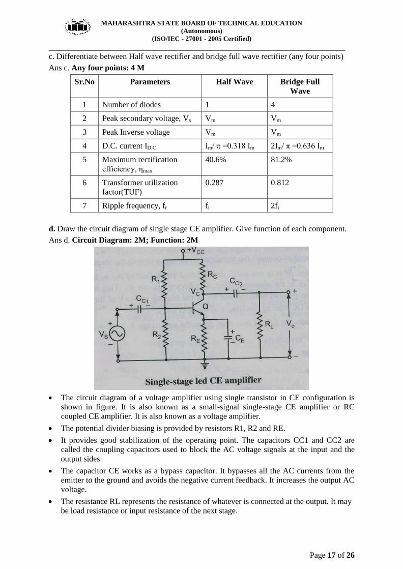
d. Draw the circuit diagram of single stage CE amplifier. Give function of each component.
Ans d. Circuit Diagram: 2M; Function: 2M
The circuit diagram of a voltage amplifier using single transistor in CE configuration is
shown in figure. It is also known as a small-signal single-stage CE amplifier or RC
coupled CE amplifier. It is also known as a voltage amplifier.
The potential divider biasing is provided by resistors R1, R2 and RE.
It provides good stabilization of the operating point. The capacitors CC1 and CC2 are
called the coupling capacitors used to block the AC voltage signals at the input and the
output sides.
The capacitor CE works as a bypass capacitor. It bypasses all the AC currents from the
emitter to the ground and avoids the negative current feedback. It increases the output AC
voltage.
The resistance RL represents the resistance of whatever is connected at the output. It may
be load resistance or input resistance of the next stage.
Sr.No Parameters Half Wave Bridge Full
Wave
1 Number of diodes 1 4
2 Peak secondary voltage, Vs Vm Vm
3 Peak Inverse voltage Vm Vm
4 D.C. current ID.C Im/ π =0.318 Im 2Im/ π =0.636 Im
5 Maximum rectification
efficiency, ηmax
40.6% 81.2%
6 Transformer utilization
factor(TUF)
0.287 0.812
7 Ripple frequency, fr fi 2fi
MAHARASHTRA STATE BOARD OF TECHNICAL EDUCATION
(Autonomous)
(ISO/IEC - 27001 - 2005 Certified)
_________________________________________________________________________
Page 18 of 26
e. Define the following for CE amplifier:
i. Bandwidth
ii. Current gain
iii. Power gain
iv. Voltage gain
Ans e. Each definition: 1M
Bandwidth:
The range of frequency over which the voltage gain of an amplifier remains constant is
known as bandwidth of an amplifier.
It is denoted as bandwidth of an amplifier.
Current Gain:
The ratio of output current to input current of a BJT amplifier is known as current gain. It is
denoted by a letter Ai
Ai = Output current/ Input current= Io/ Ii
Power Gain:
The ratio of output power to input power of a BJT amplifier is known as power gain. It is denoted
by a letter AP
AP = Output power/ Input power= Po/ Pi
Voltage Gain:
The ratio of output voltage to input voltage of a BJT amplifier is known as voltage gain. It is
denoted by a letter Av.
Av = Output voltage / Input voltage = Vo/ Vi
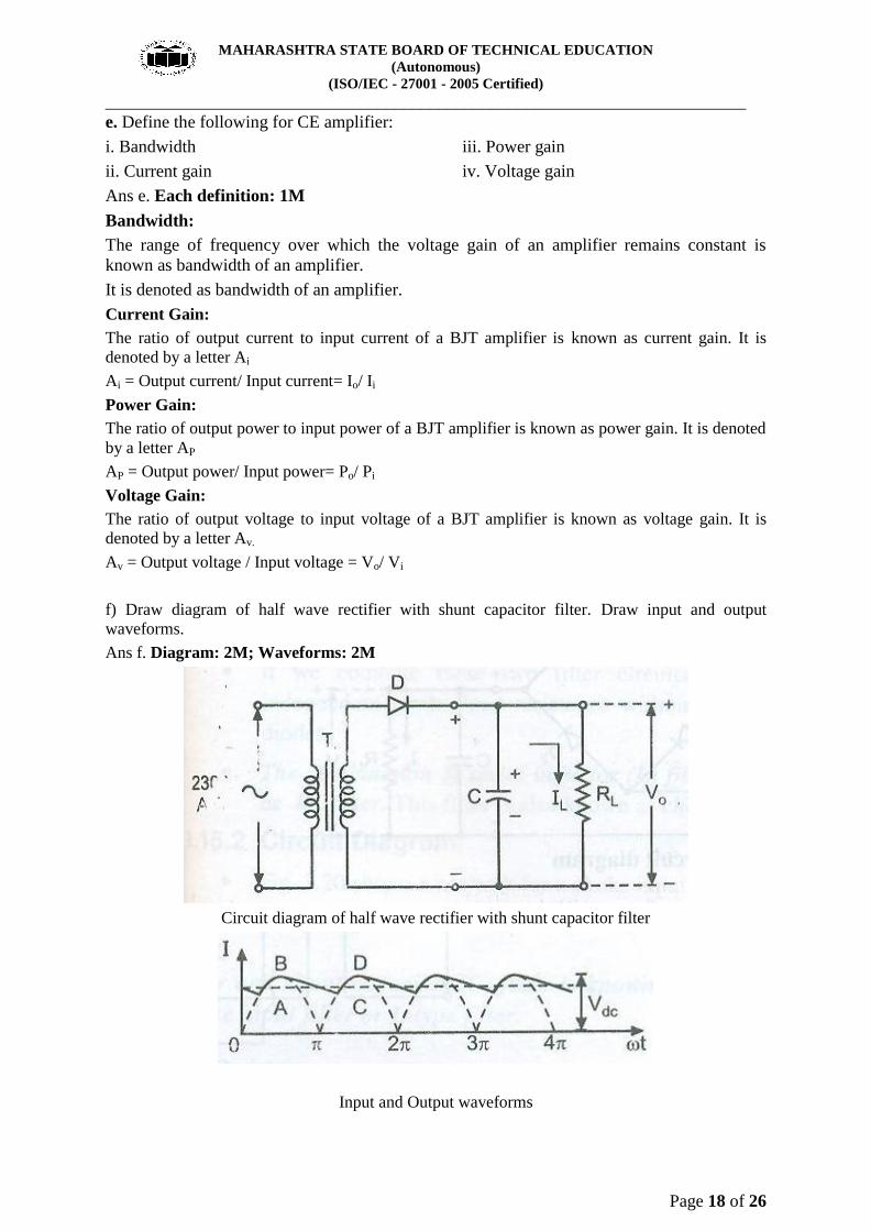
f) Draw diagram of half wave rectifier with shunt capacitor filter. Draw input and output
waveforms.
Ans f. Diagram: 2M; Waveforms: 2M
Circuit diagram of half wave rectifier with shunt capacitor filter
Input and Output waveforms
MAHARASHTRA STATE BOARD OF TECHNICAL EDUCATION
(Autonomous)
(ISO/IEC - 27001 - 2005 Certified)
_________________________________________________________________________
Page 19 of 26
5. Attempt any FOUR: 16
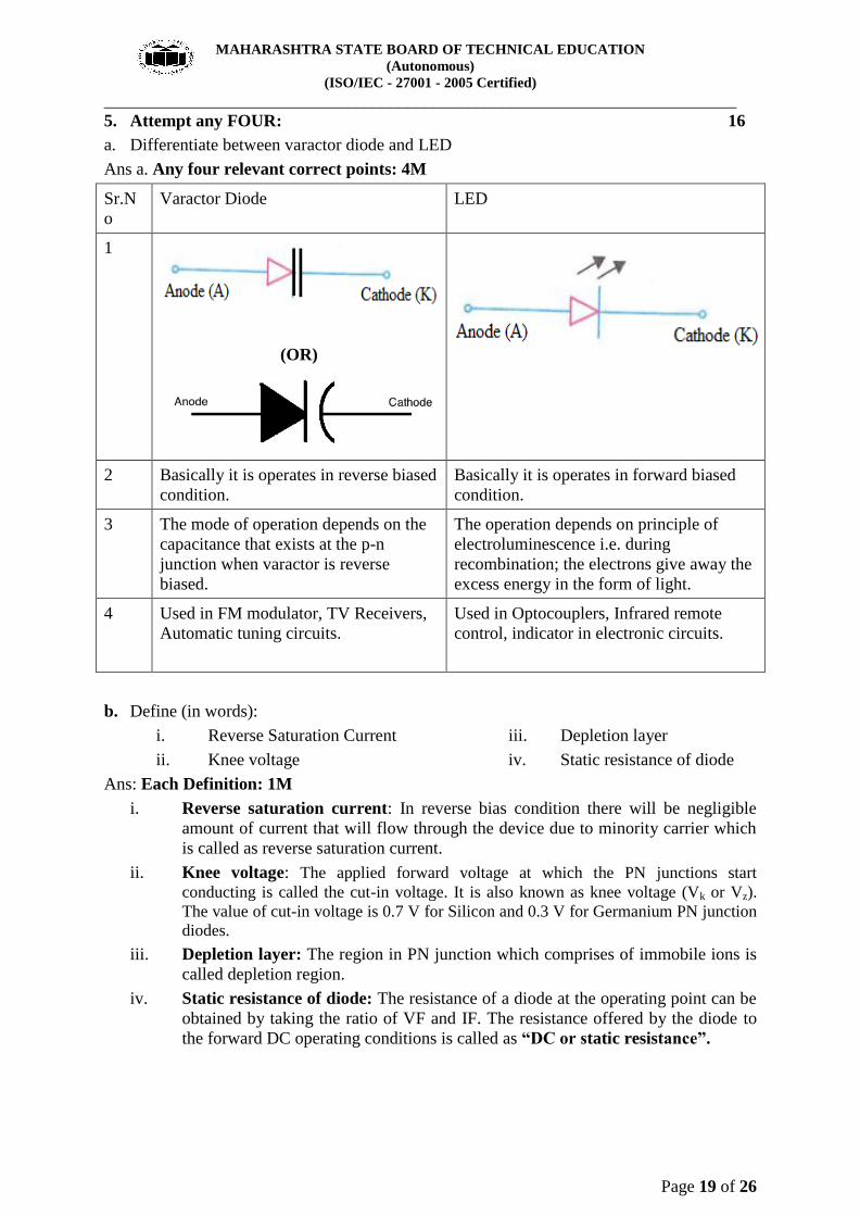
a. Differentiate between varactor diode and LED
Ans a. Any four relevant correct points: 4M
Sr.N
o
Varactor Diode LED
1
(OR)
2 Basically it is operates in reverse biased
condition.
Basically it is operates in forward biased
condition.
3 The mode of operation depends on the
capacitance that exists at the p-n
junction when varactor is reverse
biased.
The operation depends on principle of
electroluminescence i.e. during
recombination; the electrons give away the
excess energy in the form of light.
4 Used in FM modulator, TV Receivers,
Automatic tuning circuits.
Used in Optocouplers, Infrared remote
control, indicator in electronic circuits.
b. Define (in words):
i. Reverse Saturation Current
ii. Knee voltage
iii. Depletion layer
iv. Static resistance of diode
Ans: Each Definition: 1M
i. Reverse saturation current: In reverse bias condition there will be negligible
amount of current that will flow through the device due to minority carrier which
is called as reverse saturation current.
ii. Knee voltage: The applied forward voltage at which the PN junctions start
conducting is called the cut-in voltage. It is also known as knee voltage (Vk or Vz).
The value of cut-in voltage is 0.7 V for Silicon and 0.3 V for Germanium PN junction
diodes.
iii. Depletion layer: The region in PN junction which comprises of immobile ions is
called depletion region.
iv. Static resistance of diode: The resistance of a diode at the operating point can be
obtained by taking the ratio of VF and IF. The resistance offered by the diode to
the forward DC operating conditions is called as “DC or static resistance”.
MAHARASHTRA STATE BOARD OF TECHNICAL EDUCATION
(Autonomous)
(ISO/IEC - 27001 - 2005 Certified)
_________________________________________________________________________
Page 20 of 26
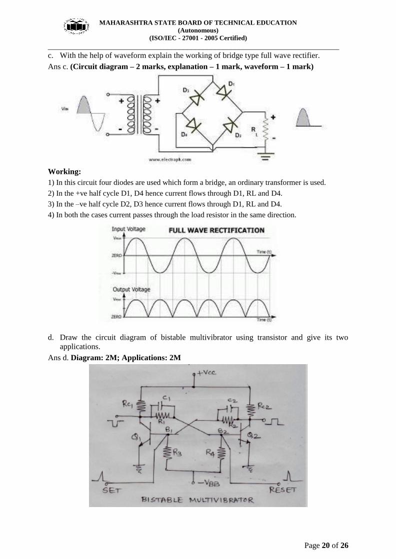
c. With the help of waveform explain the working of bridge type full wave rectifier.
Ans c. (Circuit diagram – 2 marks, explanation – 1 mark, waveform – 1 mark)
Working:
1) In this circuit four diodes are used which form a bridge, an ordinary transformer is used.
2) In the +ve half cycle D1, D4 hence current flows through D1, RL and D4.
3) In the –ve half cycle D2, D3 hence current flows through D1, RL and D4.
4) In both the cases current passes through the load resistor in the same direction.
d. Draw the circuit diagram of bistable multivibrator using transistor and give its two
applications.
Ans d. Diagram: 2M; Applications: 2M
MAHARASHTRA STATE BOARD OF TECHNICAL EDUCATION
(Autonomous)
(ISO/IEC - 27001 - 2005 Certified)
_________________________________________________________________________
Page 21 of 26
Applications: (any two)
1. It is used as a memory element in computer logic circuit.
2. It is used as a memory element in shift registers.
3. it is used as a memory element in counters.
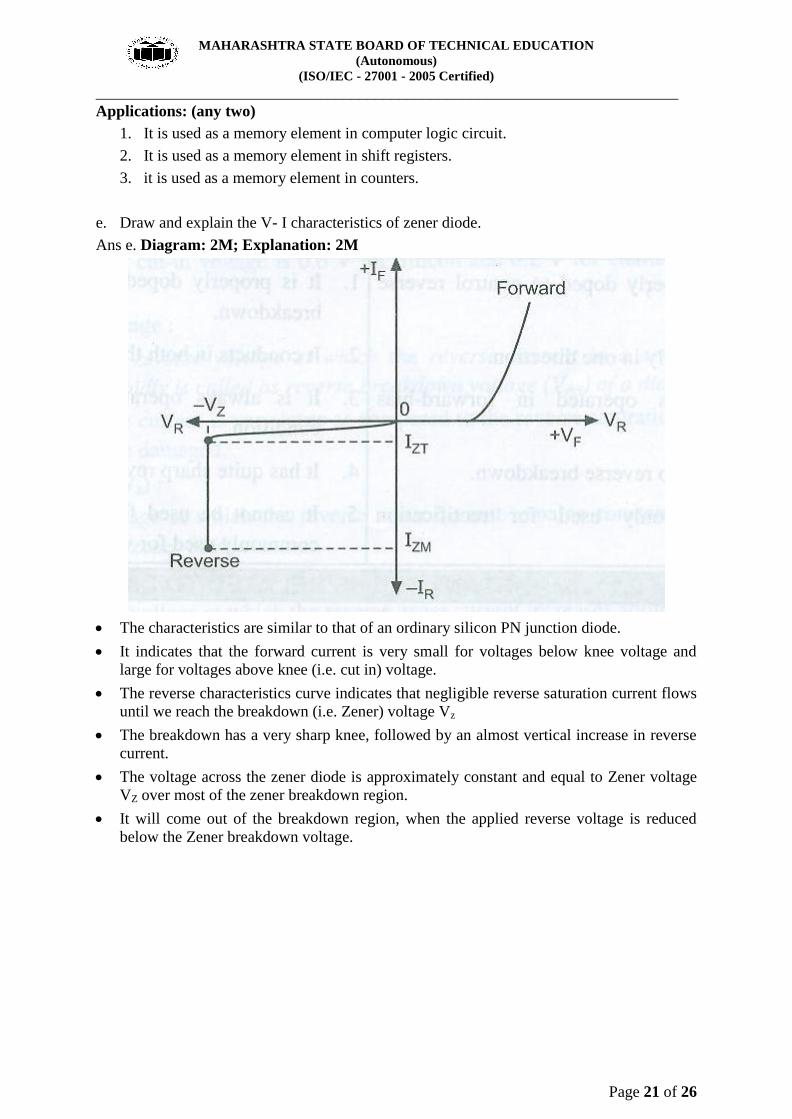
e. Draw and explain the V- I characteristics of zener diode.
Ans e. Diagram: 2M; Explanation: 2M
The characteristics are similar to that of an ordinary silicon PN junction diode.
It indicates that the forward current is very small for voltages below knee voltage and
large for voltages above knee (i.e. cut in) voltage.
The reverse characteristics curve indicates that negligible reverse saturation current flows
until we reach the breakdown (i.e. Zener) voltage Vz
The breakdown has a very sharp knee, followed by an almost vertical increase in reverse
current.
The voltage across the zener diode is approximately constant and equal to Zener voltage
VZ over most of the zener breakdown region.
It will come out of the breakdown region, when the applied reverse voltage is reduced
below the Zener breakdown voltage.
MAHARASHTRA STATE BOARD OF TECHNICAL EDUCATION
(Autonomous)
(ISO/IEC - 27001 - 2005 Certified)
_________________________________________________________________________
Page 22 of 26
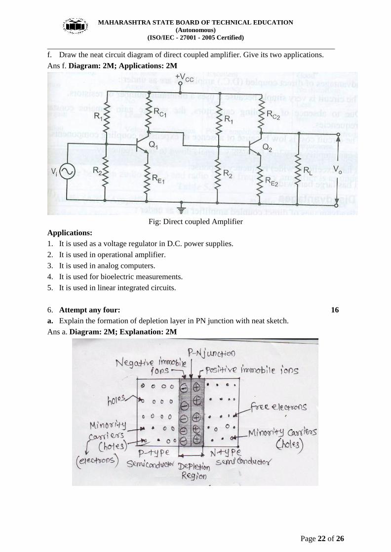
f. Draw the neat circuit diagram of direct coupled amplifier. Give its two applications.
Ans f. Diagram: 2M; Applications: 2M
Fig: Direct coupled Amplifier
Applications:
1. It is used as a voltage regulator in D.C. power supplies.
2. It is used in operational amplifier.
3. It is used in analog computers.
4. It is used for bioelectric measurements.
5. It is used in linear integrated circuits.
6. Attempt any four: 16
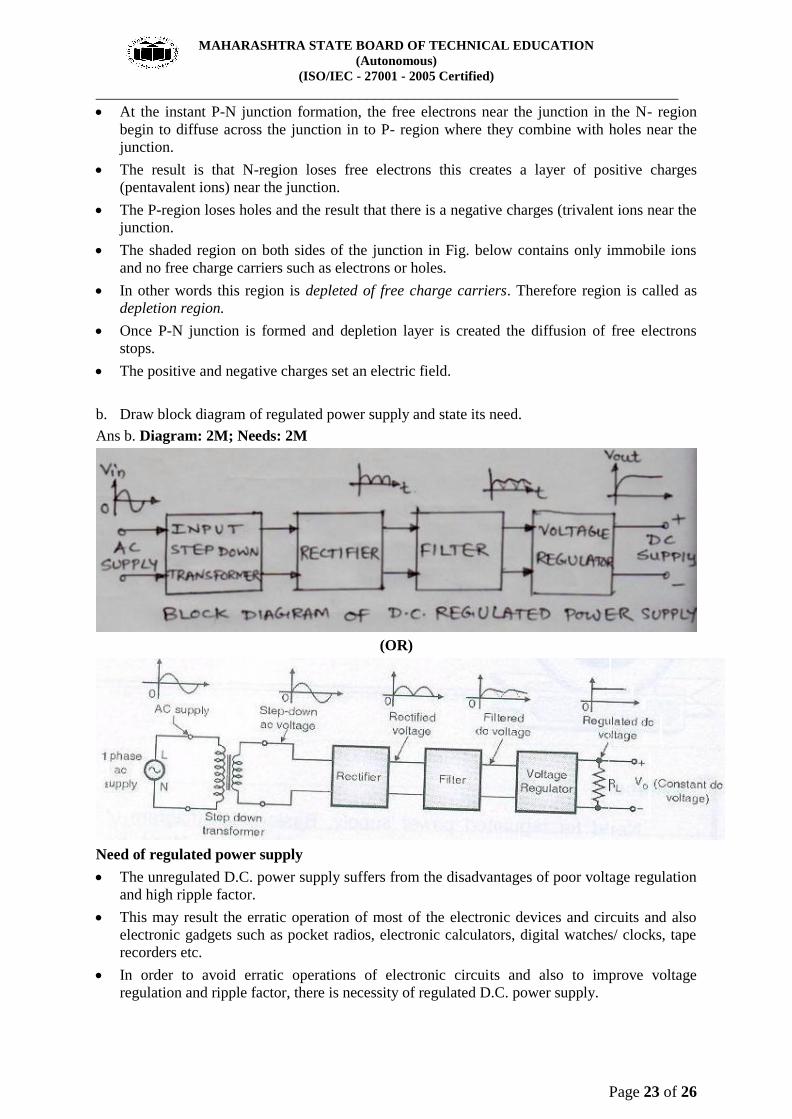
a. Explain the formation of depletion layer in PN junction with neat sketch.
Ans a. Diagram: 2M; Explanation: 2M
MAHARASHTRA STATE BOARD OF TECHNICAL EDUCATION
(Autonomous)
(ISO/IEC - 27001 - 2005 Certified)
_________________________________________________________________________
Page 23 of 26
At the instant P-N junction formation, the free electrons near the junction in the N- region
begin to diffuse across the junction in to P- region where they combine with holes near the
junction.
The result is that N-region loses free electrons this creates a layer of positive charges
(pentavalent ions) near the junction.
The P-region loses holes and the result that there is a negative charges (trivalent ions near the
junction.
The shaded region on both sides of the junction in Fig. below contains only immobile ions
and no free charge carriers such as electrons or holes.
In other words this region is depleted of free charge carriers. Therefore region is called as
depletion region.
Once P-N junction is formed and depletion layer is created the diffusion of free electrons
stops.
The positive and negative charges set an electric field.
b. Draw block diagram of regulated power supply and state its need.
Ans b. Diagram: 2M; Needs: 2M
(OR)
Need of regulated power supply
The unregulated D.C. power supply suffers from the disadvantages of poor voltage regulation
and high ripple factor.
This may result the erratic operation of most of the electronic devices and circuits and also
electronic gadgets such as pocket radios, electronic calculators, digital watches/ clocks, tape
recorders etc.
In order to avoid erratic operations of electronic circuits and also to improve voltage
regulation and ripple factor, there is necessity of regulated D.C. power supply.
MAHARASHTRA STATE BOARD OF TECHNICAL EDUCATION
(Autonomous)
(ISO/IEC - 27001 - 2005 Certified)
_________________________________________________________________________
Page 24 of 26
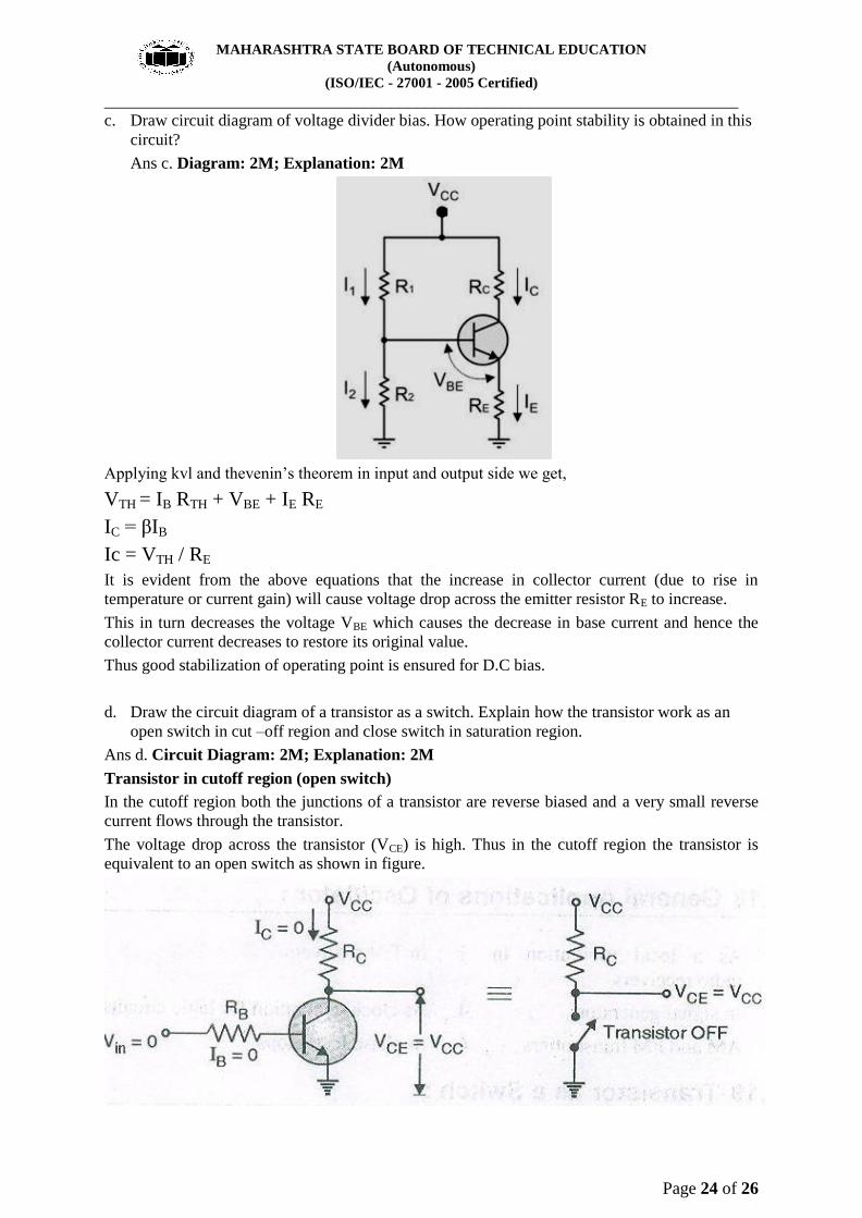
c. Draw circuit diagram of voltage divider bias. How operating point stability is obtained in this
circuit?
Ans c. Diagram: 2M; Explanation: 2M
Applying kvl and thevenin’s theorem in input and output side we get,
VTH = IB RTH + VBE + IE RE
IC = βIB
Ic = VTH / RE
It is evident from the above equations that the increase in collector current (due to rise in
temperature or current gain) will cause voltage drop across the emitter resistor RE to increase.
This in turn decreases the voltage VBE which causes the decrease in base current and hence the
collector current decreases to restore its original value.
Thus good stabilization of operating point is ensured for D.C bias.
d. Draw the circuit diagram of a transistor as a switch. Explain how the transistor work as an
open switch in cut –off region and close switch in saturation region.
Ans d. Circuit Diagram: 2M; Explanation: 2M
Transistor in cutoff region (open switch)
In the cutoff region both the junctions of a transistor are reverse biased and a very small reverse
current flows through the transistor.
The voltage drop across the transistor (VCE) is high. Thus in the cutoff region the transistor is
equivalent to an open switch as shown in figure.

MAHARASHTRA STATE BOARD OF TECHNICAL EDUCATION
(Autonomous)
(ISO/IEC - 27001 - 2005 Certified)
_________________________________________________________________________
Page 25 of 26
Transistor in the saturation region:
When Vin is positive, a large base current flows and the transistor saturates.
In the saturation region both the junctions of a transistor are forward biased. The voltage drop
across the transistor (VCE) is very small of the order of 0.2V to 1 V depending on the type of
transistor and collector current is very large.
In saturation the transistor is equivalent to a closed switch as shown in figure.
e. Draw the transfer characteristics of JFET. Give the meaning of IdSS and VgSoff.
Ans e. Diagram: 2M; Meaning of IdSS: 1M; Meaning of VgSoff: 1M
IDSS: The maximum amount of drain current at zero gate- to- source voltage VGS is known as
drain saturation current. It is denoted by IDSS and is specified by the manufacturer.
VGS (off): The gate- to- source voltage VGS at which the drain current is reduced to zero (or
completely cut- off) is called pinch- off voltage. It is designated by a letter VP or VGS (off).
MAHARASHTRA STATE BOARD OF TECHNICAL EDUCATION
(Autonomous)
(ISO/IEC - 27001 - 2005 Certified)
_________________________________________________________________________
Page 26 of 26
f. An A.C. supply of 230V is applied to half wave rectifier circuit through a transformer of turns
ratio 2:1 Calculate
i. DC output voltage------ 2M
ii. PIV of diode------------- 2M
Ans f.
Given: V1= 230V
N2/N1 = 1/ 2
1. We know that secondary voltage
V2 = N2/N1 x V1
= 230x 1/ 2
= 115V
Maximum value of secondary voltage
Vm= √ x V2
= √ x 115V
= 162.6 volts
Therefore, DC voltage
Vdc= Vm /π = 162.6/ 3.14 = 51.7 volts
2. PIV of diode
PIV of diode = Vm= 162.6 volts