magnetic recording and nand flash areal densities a
TRANSCRIPT
Magnetic Recording and NAND Flash Areal DensitiesA Lithographic Perspective¹
Robert Fontana, IBM Systems Technology Group, San Jose, CASteven Hetzler, IBM Research Division, San Jose, CA
1. Variation on 2008 INTERMAG Paper, “Thin Film Processing Realities for Tbit/in² Recording”by R. Fontana, N. Robertson, S. Hetzler
1
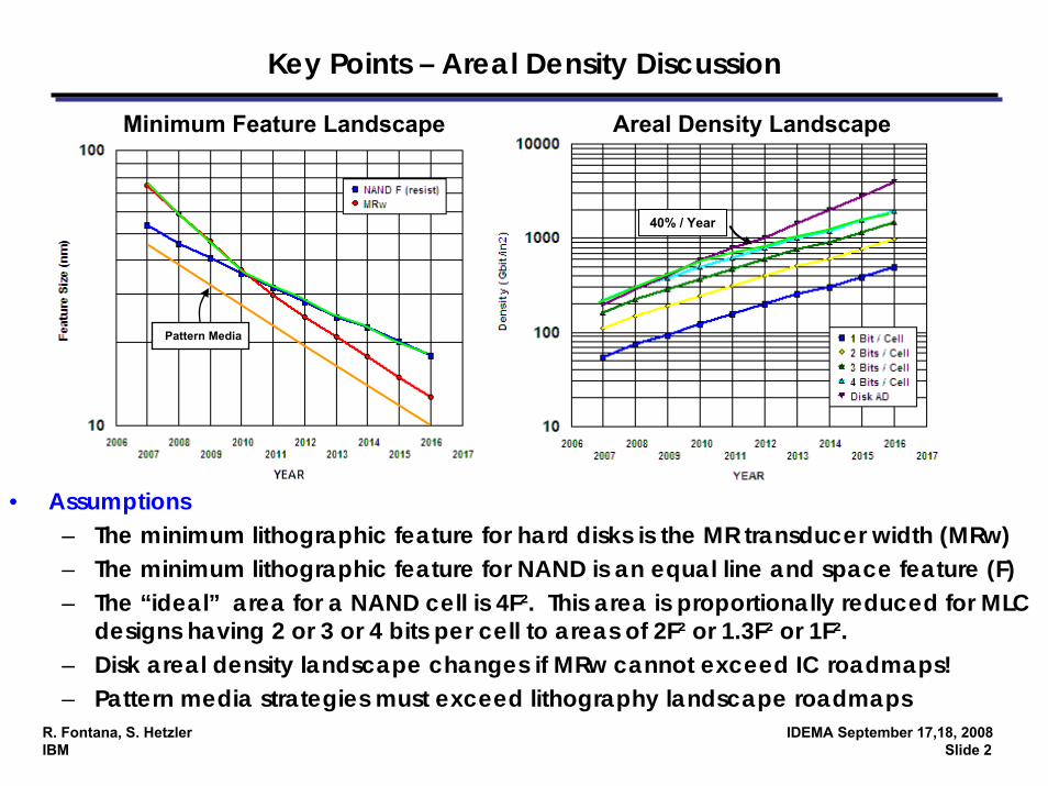
Key Points – Areal Density Discussion
Minimum Feature Landscape Areal Density Landscape
• Assumptions– The minimum lithographic feature for hard disks is the MR transducer width (MRw)– The minimum lithographic feature for NAND is an equal line and space feature (F)– The “ideal” area for a NAND cell is 4F². This area is proportionally reduced for MLC
designs having 2 or 3 or 4 bits per cell to areas of 2F² or 1.3F² or 1F². – Disk areal density landscape changes if MRw cannot exceed IC roadmaps!– Pattern media strategies must exceed lithography landscape roadmaps
Pattern Media
40% / Year
R. Fontana, S. Hetzler IDEMA September 17,18, 2008IBM Slide 2
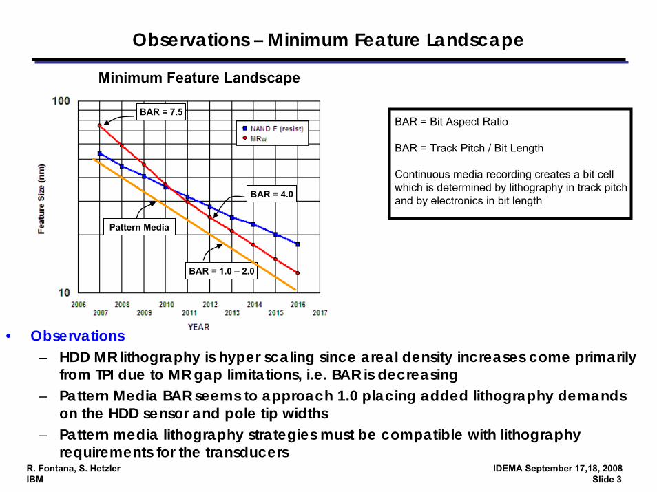
Observations – Minimum Feature Landscape
Minimum Feature Landscape
BAR = 1.0 – 2.0
BAR = 7.5
BAR = 4.0
• Observations– HDD MR lithography is hyper scaling since areal density increases come primarily
from TPI due to MR gap limitations, i.e. BAR is decreasing– Pattern Media BAR seems to approach 1.0 placing added lithography demands
on the HDD sensor and pole tip widths– Pattern media lithography strategies must be compatible with lithography
requirements for the transducers
BAR = Bit Aspect Ratio
BAR = Track Pitch / Bit Length
Continuous media recording creates a bit cell which is determined by lithography in track pitchand by electronics in bit length
Pattern Media
R. Fontana, S. Hetzler IDEMA September 17,18, 2008IBM Slide 3
GOALS
• QUESTIONS– In 2012, when 1 Tbit/in² areal densities are forecasted for hard disk
products, will film head structures be lithographically compatible with integrated circuit (IC) lithography roadmaps?
– After 2012, should the industry transition to patterned bit media or to patterned track media, how will disk lithography requirements compare with integrated circuit (IC) lithography roadmaps?
– Independent of disk patterning issues, can lithography for the thin film transducer be sustained?
• OUTLINE– Recording bit cell and IC bit cell comparisons– Semiconductor lithography roadmap (2007 – 2019)– 1 Tbit/in² film head dimensions and IC roadmaps in 2012– Overlay control and CD (critical dimension) control for thin film heads– Lithography roadmap implications for patterned bits and / or
patterned media R. Fontana, S. Hetzler IDEMA September 17,18, 2008IBM Slide 4
Magnetic and NAND Bit Cell Comparisons
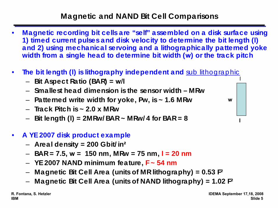
• Magnetic recording bit cells are “self” assembled on a disk surface using 1) timed current pulses and disk velocity to determine the bit length (l) and 2) using mechanical servoing and a lithographically patterned yoke width from a single head to determine bit width (w) or the track pitch
• The bit length (l) is lithography independent and sub lithographic– Bit Aspect Ratio (BAR) = w/l– Smallest head dimension is the sensor width – MRw– Patterned write width for yoke, Pw, is ~ 1.6 MRw– Track Pitch is ~ 2.0 x MRw– Bit length (l) = 2MRw/BAR ~ MRw/4 for BAR = 8
• A YE 2007 disk product example– Areal density = 200 Gbit/in²– BAR = 7.5, w = 150 nm, MRw = 75 nm, l = 20 nm– YE 2007 NAND minimum feature, F ~ 54 nm– Magnetic Bit Cell Area (units of MR lithography) = 0.53 F²– Magnetic Bit Cell Area (units of NAND lithography) = 1.02 F²
l
w
l
R. Fontana, S. Hetzler IDEMA September 17,18, 2008IBM Slide 5
Magnetic and NAND Bit Cell Comparisons
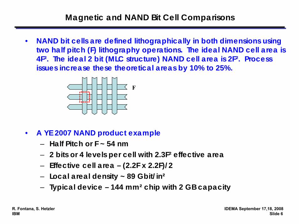
• NAND bit cells are defined lithographically in both dimensions using two half pitch (F) lithography operations. The ideal NAND cell area is 4F². The ideal 2 bit (MLC structure) NAND cell area is 2F². Process issues increase these theoretical areas by 10% to 25%.
• A YE 2007 NAND product example– Half Pitch or F ~ 54 nm– 2 bits or 4 levels per cell with 2.3F² effective area– Effective cell area – (2.2F x 2.2F)/2– Local areal density ~ 89 Gbit/in²– Typical device – 144 mm² chip with 2 GB capacity
F
R. Fontana, S. Hetzler IDEMA September 17,18, 2008IBM Slide 6
Magnetic and NAND Bit Cell Comparisons
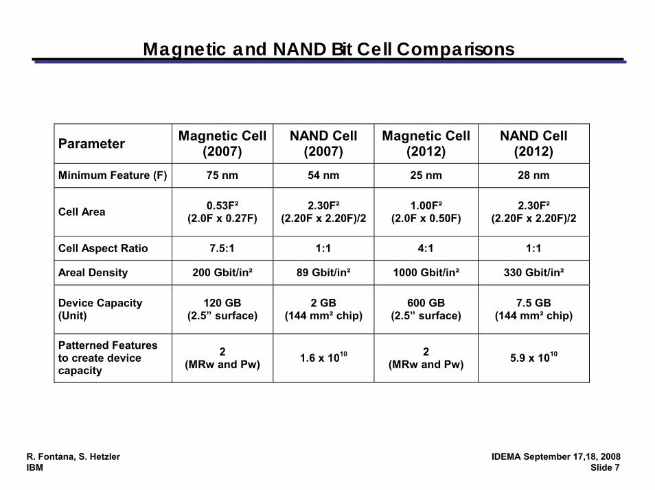
Parameter Magnetic Cell (2007)
NAND Cell (2007)
Magnetic Cell (2012)
NAND Cell (2012)
Minimum Feature (F) 75 nm 54 nm 25 nm 28 nm
Cell Area 0.53F² (2.0F x 0.27F)
2.30F² (2.20F x 2.20F)/2
1.00F² (2.0F x 0.50F)
2.30F² (2.20F x 2.20F)/2
Cell Aspect Ratio 7.5:1 1:1 4:1 1:1
Areal Density 200 Gbit/in² 89 Gbit/in² 1000 Gbit/in² 330 Gbit/in²
Device Capacity (Unit)
120 GB (2.5” surface)
2 GB (144 mm² chip)
600 GB (2.5” surface)
7.5 GB (144 mm² chip)
Patterned Features to create device capacity
2 (MRw and Pw) 1.6 x 10¹⁰ 2
(MRw and Pw) 5.9 x 10¹⁰
R. Fontana, S. Hetzler IDEMA September 17,18, 2008IBM Slide 7
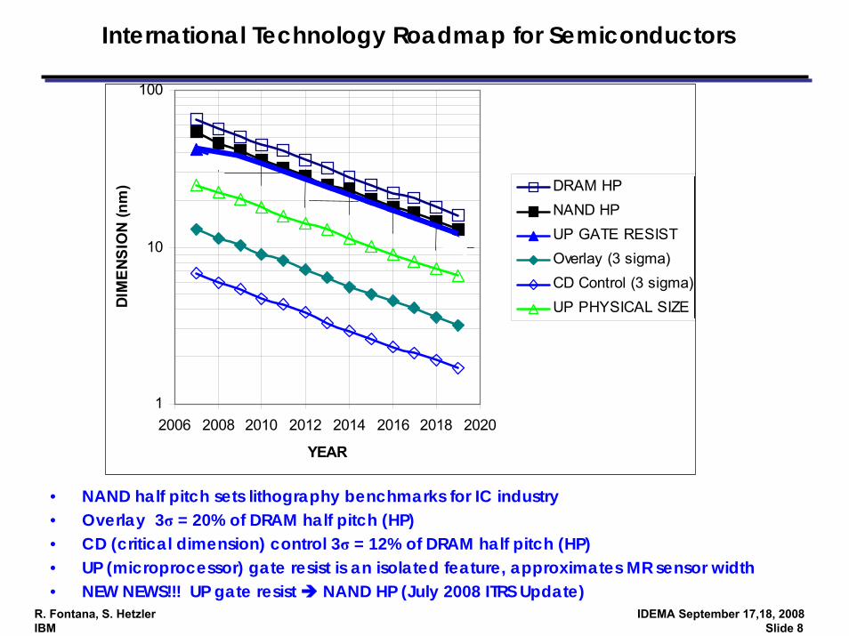
International Technology Roadmap for Semiconductors
1
10
100
2006 2008 2010 2012 2014 2016 2018 2020
YEAR
DIM
EN
SIO
N (n
m) DRAM HP
NAND HPUP GATE RESISTOverlay (3 sigma)CD Control (3 sigma)UP PHYSICAL SIZE
• NAND half pitch sets lithography benchmarks for IC industry• Overlay 3σ = 20% of DRAM half pitch (HP)• CD (critical dimension) control 3σ = 12% of DRAM half pitch (HP)• UP (microprocessor) gate resist is an isolated feature, approximates MR sensor width• NEW NEWS!!! UP gate resist NAND HP (July 2008 ITRS Update)
R. Fontana, S. Hetzler IDEMA September 17,18, 2008IBM Slide 8
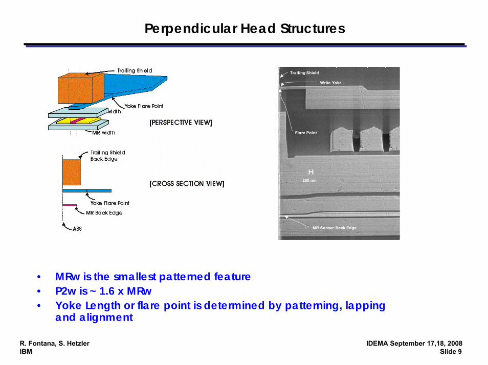
Perpendicular Head Structures
, p ( ), p ( )
200 nm
Trailing Shield
Write Yoke
MR Sensor Back Edge
Flare Point
, p ( ), p ( )
200 nm
Trailing Shield
Write Yoke
MR Sensor Back Edge
Flare Point
• MRw is the smallest patterned feature• P2w is ~ 1.6 x MRw• Yoke Length or flare point is determined by patterning, lapping
and alignment
R. Fontana, S. Hetzler IDEMA September 17,18, 2008IBM Slide 9
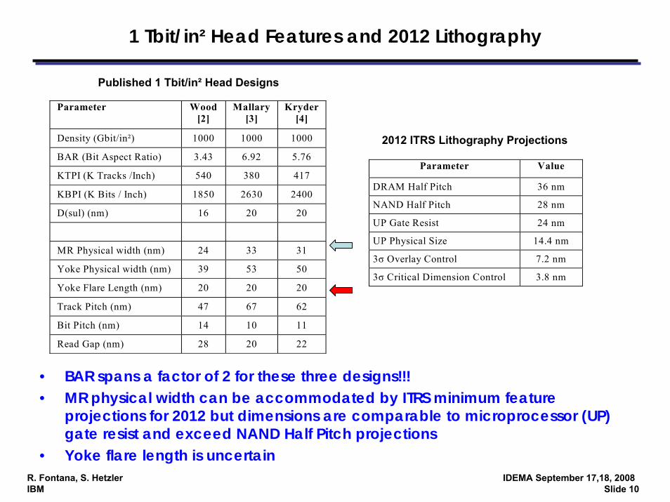
1 Tbit/in² Head Features and 2012 Lithography
• BAR spans a factor of 2 for these three designs!!!• MR physical width can be accommodated by ITRS minimum feature
projections for 2012 but dimensions are comparable to microprocessor (UP) gate resist and exceed NAND Half Pitch projections
• Yoke flare length is uncertain
Parameter Wood
[2] Mallary
[3] Kryder
[4]
Density (Gbit/in²) 1000 1000 1000
BAR (Bit Aspect Ratio) 3.43 6.92 5.76
KTPI (K Tracks /Inch) 540 380 417
KBPI (K Bits / Inch) 1850 2630 2400
D(sul) (nm) 16 20 20
MR Physical width (nm) 24 33 31
Yoke Physical width (nm) 39 53 50
Yoke Flare Length (nm) 20 20 20
Track Pitch (nm) 47 67 62
Bit Pitch (nm) 14 10 11
Read Gap (nm) 28 20 22
Parameter Value
DRAM Half Pitch 36 nm
NAND Half Pitch 28 nm
UP Gate Resist 24 nm
UP Physical Size 14.4 nm
3σ Overlay Control 7.2 nm
3σ Critical Dimension Control 3.8 nm
2012 ITRS Lithography Projections
Published 1 Tbit/in² Head Designs
R. Fontana, S. Hetzler IDEMA September 17,18, 2008IBM Slide 10
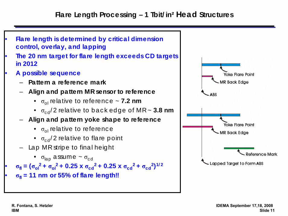
Flare Length Processing – 1 Tbit/in² Head Structures
• Flare length is determined by critical dimension control, overlay, and lapping
• The 20 nm target for flare length exceeds CD targets in 2012
• A possible sequence– Pattern a reference mark– Align and pattern MR sensor to reference
• σol relative to reference ~ 7.2 nm• σcd/2 relative to back edge of MR ~ 3.8 nm
– Align and pattern yoke shape to reference• σol relative to reference• σcd/2 relative to flare point
– Lap MR stripe to final height• σlap assume ~ σcd
• σfl = (σol2 + σol
2 + 0.25 x σcd2 + 0.25 x σcd
2 + σcd2)1/2
• σfl = 11 nm or 55% of flare length!!
R. Fontana, S. Hetzler IDEMA September 17,18, 2008IBM Slide 11
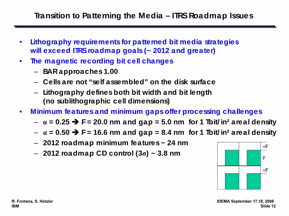
Transition to Patterning the Media – ITRS Roadmap Issues
• Lithography requirements for patterned bit media strategies will exceed ITRS roadmap goals (~ 2012 and greater)
• The magnetic recording bit cell changes– BAR approaches 1.00– Cells are not “self assembled” on the disk surface – Lithography defines both bit width and bit length
(no sublithographic cell dimensions)• Minimum features and minimum gaps offer processing challenges
– α = 0.25 F = 20.0 nm and gap = 5.0 nm for 1 Tbit/in² areal density– α = 0.50 F = 16.6 nm and gap = 8.4 nm for 1 Tbit/in² areal density– 2012 roadmap minimum features ~ 24 nm– 2012 roadmap CD control (3σ) ~ 3.8 nm
R. Fontana, S. Hetzler IDEMA September 17,18, 2008IBM Slide 12
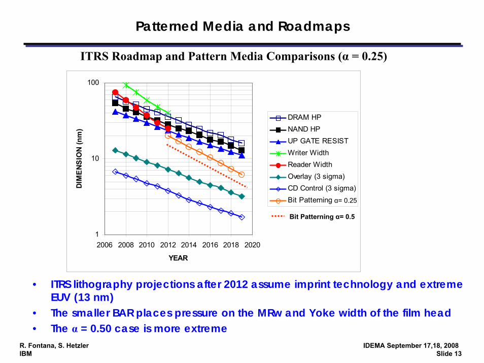
Patterned Media and Roadmaps
ITRS Roadmap and Pattern Media Comparisons (α = 0.25)
1
10
100
2006 2008 2010 2012 2014 2016 2018 2020
YEAR
DIM
ENSI
ON
(nm
)
DRAM HPNAND HPUP GATE RESISTWriter WidthReader WidthOverlay (3 sigma)CD Control (3 sigma)Bit Patterning α= 0.25
Bit Patterning α= 0.5
• ITRS lithography projections after 2012 assume imprint technology and extreme EUV (13 nm)
• The smaller BAR places pressure on the MRw and Yoke width of the film head• The α = 0.50 case is more extreme
R. Fontana, S. Hetzler IDEMA September 17,18, 2008IBM Slide 13
Summary
• Today, NAND cell densities are approaching 100 Gbit/in²
• The thin film processing of 1 Tbit/in² film heads in the 2012 time frame is realizable– MRw minimum feature will require “state of the art” lithography
tooling rather than tooling lagging NAND strategies by 2 – 3 years– Better alignment tooling and improved flare tolerance designs
will be required
• Patterned bit media requires advancements and strategies exceeding the ITRS roadmap projections.
• Any advanced bit patterning strategy still requires a film transducer with minimum features sufficient to “read” and “write” the bits
• If NAND could meet the 2012 goal of 20 nm features required by patterned media for 1 Tbit/in² areal density, the NAND areal density could be 0.65 Tbit/in².
R. Fontana, S. Hetzler IDEMA September 17,18, 2008IBM Slide 14
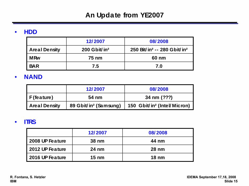
An Update from YE2007
• HDD
• NAND
• ITRS
12/2007 08/2008Areal Density 200 Gbit/in² 250 Bit/in² -- 280 Gbit/in²MRw 75 nm 60 nmBAR 7.5 7.0
12/2007 08/2008F (feature) 54 nm 34 nm (???)Areal Density 89 Gbit/in² (Samsung) 150 Gbit/in² (Intel/Micron)
12/2007 08/20082008 UP Feature 38 nm 44 nm2012 UP Feature 24 nm 28 nm2016 UP Feature 15 nm 18 nm
R. Fontana, S. Hetzler IDEMA September 17,18, 2008IBM Slide 15