magnetic flux leakage testing for back-side defects using
TRANSCRIPT

Magnetic Flux Leakage Testing
for Back-side Defects Using a Tunnel Magnetoresistive Device
Yuya Tsukamoto, Keisyu Shiga,
Kenji Sakai, Toshihiko Kiwa, Keiji Tsukada
Graduate School of Natural Science and Technology,
Okayama University
Okayama, Japan
e-mail: (en421440, pcf45clo)@s.okayama-u.ac.jp
(sakai-k, kiwa, tsukada)@cc.okayama-u.ac.jp
Yasuhiro Honda
KONICA MINOLTA, INC.
Osaka, Japan
e-mail: [email protected]
Abstract— Magnetic non-destructive testing is limited to
surface inspection, however demand for the detection of
deep defects is increasing. Therefore, we developed a
magnetic flux leakage (MFL) system using a tunnel
magnetoresistive (TMR) device that has high sensitivity
and wide frequency range in order to detect deep defects.
Using the developed system, back-side pits of steel plates
having different depth and diameter were measured and
2D images were created. Moreover, we analyzed the
detected vector signal with optimized phase data. As a
result, the developed MFL system can detect a defect
that has a wall thinning rate of more than 56 % of 8.6
mm thick steel plates. Furthermore, the defect’s
diameter size was estimated by spatial signal change.
Keywords-MFL; magnetic imaging; TMR device; Low-
Freaquency field; back-side pit.
I. INTRODUCTION
Accidents due to defects in steel structures such as power plants or pipe line cause serious injuries to humans and harm to the natural environment. Therefore, it is important to use non-destructive testing for detecting defects at an early stage. In many cases, it is difficult to find defects in the interior or on the back side, and thus a detection method for deep defects is desired. There are many non-destructive testing methods such as radiographic testing [1], ultrasonic testing [2], magnetic flux leakage (MFL) testing [3]-[9], and eddy current testing (ECT) [10]. Among them, MFL is commonly used for ferromagnetic material such as steel and it is a method for detecting flux with bypass defects due to differences in permeability and leakage from the sample’s surface when an external field is applied to the sample.
MFL for deep defects needs to be operated at low frequency because the penetration of the applied external field becomes deeper with decreasing frequency. However, the conventional MFL method, which uses a detection coil as a magnetic sensor, cannot be operated at low frequency because it has low sensitivity at low frequency due to Faraday’s law of induction. Therefore, it can detect only surface defects near the detection coil. Moreover, the
detection of deep defects also requires a high magnetic resolution because the change of flux generated by the deep defect is very small. The other problem of MFL is that the magnetic field intensity of MFL needs to be operated at the saturation region of the B-H curve in order to obtain measurable large magnetic flux leakage. However, a measurement system that gives such large magnetic field intensity is costly because a high power current source is necessary. One way to solve these problems is to use a high sensitivity magnetic sensor that can detect a low magnetic intensity field at low frequency such as a magnetoresistive (MR) sensor. If such a sensor were installed, we could operate MFL at extra low frequency, which would give deep skin depth and detect small magnetic flux leakage caused by a low power source. We reported a MFL system using an anisotropic magnetoresistive (AMR) sensor [11]. Recently, the tunnel magnetoresistive (TMR) sensor has progressed because it has a larger MR ratio than other MR devices with a wide frequency range.
In this study, we developed the MFL system using a TMR device having high sensitivity at extreme-low frequency in order to enable us to detect defects deeper and more clearly than the AMR sensor and other magnetic sensors. Moreover, we investigated the performance of the developed system using samples having various back-side pits.
II. TMR DEVICE
A TMR device is a kind of MR device and is usually applied in the magnetic head of a hard disk. It has a larger MR ratio than other MR devices. A common TMR device shows a step response to magnetic fields and has hysteresis. The TMR device used in this study was designed for sensor application [12]-[14]. It was annealed at different temperatures and directions two times in order to make easy directions of the pin layer and the free layer orthogonal. In this structure, the output is linear with respect to the magnetic field. In addition, it has a large MR ratio because of magnetic coupling of the free layer and the soft magnetic material layer. Figure 1 shows the TMR resistance as a
function of an applied field. The range from -400 T to
114Copyright (c) IARIA, 2014. ISBN: 978-1-61208-375-9
SENSORDEVICES 2014 : The Fifth International Conference on Sensor Device Technologies and Applications

0
400
800
1200
1600
-1000 -500 0 500 1000Applied Field (μT)
Res
ista
nce
(Ω
)
Measurement range
Figure 1. Resistance of the TMR device to an applied field.
400 T, which is treated in MFL, can be applicable to the sensor application.
III. EXPERIMENTAL
The developed MFL system (Figure 2) consists of a sensor probe with a TMR device, a lock-in amplifier, a current source, an oscillator, two excitation coils, a half shaped ferrite yoke, a sample stage, and a PC. Two excitation coils with 30 turns were connected to both ends of the yoke and an AC field was induced in the sample between both ends. The sensor probe was installed between the ends of the yoke and they were 1 mm away from the sample’s surface. The TMR device measured magnetic flux leakage bypassing defects. In this study, the TMR device had sensitivity to the direction parallel to both ends of the yoke in order to obtain a larger output [11]. The excitation coils were operated by a sine wave of 1.2 App and 5 Hz or 10 Hz from the current source controlled by the oscillator. The effect of the eddy current can be ignored in such an extreme-low frequency field. The output signal from the TMR device was detected by the lock-in amplifier, which is synchronized with the current source in order to obtain a high signal-to-noise ratio.
The signal from the lock-in amplifier contains the signal intensity R and the phase θ. In this measurement system, magnetic flux leakage is very small so that it is strongly affected by the phase shift of the entire measurement system. Therefore, we calculated the imaginary part of the signal intensity with the common phase φ [11].
R’ = R sin(θ+φ )
Here, φ is a common phase adjusting the phase shift of the entire measurement system.
The samples used in this study were two steel plates (SPHC) with four back-side pits as shown in Figure 3. Both samples were 8.6 mm thick. The pits of Sample (a) are of the same diameter (6 mm) and different wall thinning rates (23, 57, 70, 93 %). Sample (b) has the same wall thinning rate (70 %) and different diameters (4, 6, 8. 10 mm). Multipoint measurement was carried out in the range of 20 mm × 20 mm around a pit from front surface with an interval of 1 mm for 21 × 21 steps as shown in Figure4.
X-Y Stage
Lock-in Amplifier
Current Source
Oscillator
PC
Ref in
Excitation Coil
TMR Device
Figure 2. Schematic diagram of the developed MFL system.
We investigated the common phase φ in this measurement system. The measurement was carried out around a pit that has a wall thinning rate of 70% and a diameter of 4 mm. The excitation coils were operated by sine wave of 1.2 App and 10 Hz or 5 Hz from the current source. The measurement results show as contour maps of calculated intensity (mV) with different common phases.
Figure 5 shows magnetic images with a frequency of 10 Hz and different common phases and Figure 6 shows that with 5 Hz and different common phases. Magnetic images with a common phase φ of 130 ° show the emphasis of the intensity change due to the pit in the center of the scanning range. The magnetic image with a frequency of 5 Hz shows the presence of the back-side pit more clearly than that of 10 Hz because the skin depth becomes deeper with decreasing frequency. Therefore, the frequency was 5 Hz and the optimized common phase φ was 130 ° for the measurement system.
Figure 7 shows the power spectrum of the developed system when the magnetic field was not applied and the sine
field was applied at 100 T and 5 Hz in the unshielded environment. The sensitivity at 5 Hz of the developed system
is 2.44 mV/T. We estimated the magnetic noise without an applied field that corresponds to the minimum magnetic field resolution at 5 Hz. As a result, the magnetic field resolution was 1.08 nT.
8.6 mm
200 mm
200 m
m
30 mm
50 m
m
23 % 57 %
93 % 70 %
(a) Fixed diameter, different wall thinning rates.
115Copyright (c) IARIA, 2014. ISBN: 978-1-61208-375-9
SENSORDEVICES 2014 : The Fifth International Conference on Sensor Device Technologies and Applications

8.6 mm
200 m
m
4 mm 6 mm
10 mm 8 mm
30 mm
50 m
m
200 mm
(b) Fixed wall thinning rate, different diameters.
Figure 3. Schematic diagram of the test plates with pits.
20 mm
20 mm
Figure 4. Measuring points for back-side pits.
φ = 0 °
0 10 200
10
20
43.22
45.10
46.96
φ = 50 °
0 10 200
10
20
142.7
145.0
147.2
φ = 90 °
0 10 200
10
20
149.8
151.3
152.8
φ = 130 °
0 10 200
10
20
86.27
87.10
87.92
0 10 200
10
20
-49.44
-46.64
-43.86
φ = 170°
Mag
net
ic i
nte
nsi
ty (
mV
)
Scanning distance (mm)
Sca
nn
ing d
ista
nce
(m
m)
Mag
net
ic I
nte
nsi
ty (
mV
)
Figure 5. Magnetic images with 10 Hz and different phase.
φ = 0 °
0 10 200
10
20
27.24
28.25
29.26
φ = 50 °
0 10 200
10
20
120.0
121.1
122.1
φ = 90 °
0 10 200
10
20
133.5
134.4
135.3
φ = 130 °
0 10 200
10
20
84.08
84.93
85.78
φ = 170 °
0 10 200
10
20
-5.440
-4.456
-3.471
Figure 6. Magnetic images with 5 Hz and different phase.
0.0001
0.001
0.01
0.1
1
10
100
1000
0.1 1 10 100
Non-field
100 μT
103
102
10
1
10-1
10-2
10-3
10-4
Frequency (Hz)
Am
pli
tude
(mV
/√H
z)
Figure 7. Power spectrum of the developed system.
To evaluate the performance of the developed MFL
system, we analyzed the magnetic image change of a steel plate having different pit wall thinning rates and diameters under optimum conditions. The excitation coils were operated by a sine wave of 5 Hz and 1.2 App from the current source. We calculated the signal vector with the optimized phase φ = 130°. The aforementioned Sample (a) and Sample (b) were measured and we made contour maps of the calculated signal vector.
IV. RESULTS AND DISCUSSION
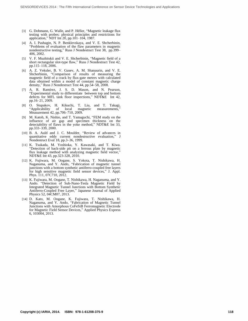
First, we used Sample (a) and investigated the change of magnetic images of the steel plates with different wall thinning rates. The map showed the existence of the pit and it becomes clear with increasing the actual pit’s wall thinning rate (Figure 8). However, the magnetic image of a pit that has a wall thinning rate of 23 % is unclear. This was caused by the weak magnetic flux leakage from the small thinning rate of the wall. The detection limit was a thinning rate of
116Copyright (c) IARIA, 2014. ISBN: 978-1-61208-375-9
SENSORDEVICES 2014 : The Fifth International Conference on Sensor Device Technologies and Applications
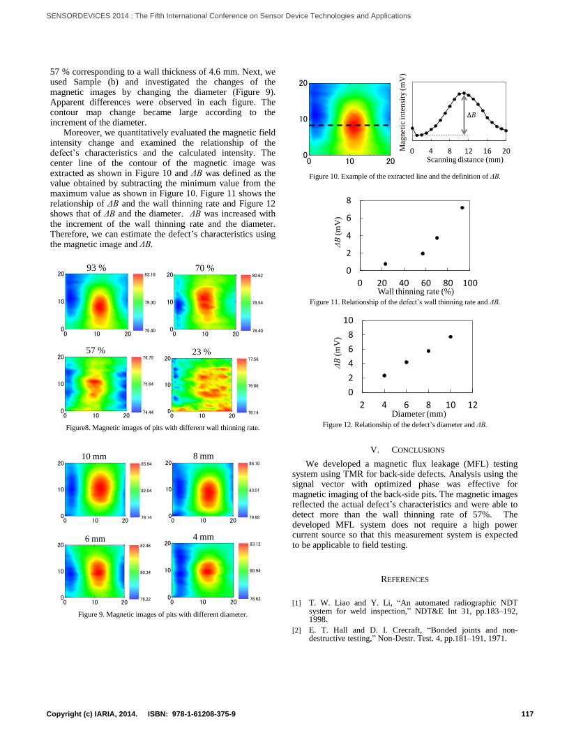
57 % corresponding to a wall thickness of 4.6 mm. Next, we used Sample (b) and investigated the changes of the magnetic images by changing the diameter (Figure 9). Apparent differences were observed in each figure. The contour map change became large according to the increment of the diameter.
Moreover, we quantitatively evaluated the magnetic field intensity change and examined the relationship of the defect’s characteristics and the calculated intensity. The center line of the contour of the magnetic image was extracted as shown in Figure 10 and ΔB was defined as the value obtained by subtracting the minimum value from the maximum value as shown in Figure 10. Figure 11 shows the relationship of ΔB and the wall thinning rate and Figure 12 shows that of ΔB and the diameter. ΔB was increased with the increment of the wall thinning rate and the diameter. Therefore, we can estimate the defect’s characteristics using the magnetic image and ΔB.
0 10 200
10
20
75.40
79.30
83.1693 %
0 10 200
10
20
76.40
78.54
80.6270 %
0 10 200
10
20
74.44
75.64
76.7557 %
0 10 200
10
20
76.14
76.86
77.56
23 %
Figure8. Magnetic images of pits with different wall thinning rate.
0 10 200
10
20
78.14
82.04
85.94
10 mm
0 10 20
0
10
20
79.88
83.01
86.10
8 mm
0 10 200
10
20
78.22
80.34
82.466 mm
0 10 20
0
10
20
78.62
80.94
83.124 mm
Figure 9. Magnetic images of pits with different diameter.
0 4 8 12 16 20Scanning distance (mm)0 10 20
0
10
20
75.40
79.30
83.16
Magneti
c inte
nsi
ty (
mV
)
Figure 10. Example of the extracted line and the definition of ΔB.
0
2
4
6
8
0 20 40 60 80 100Wall thinning rate (%)
ΔB
(mV
)
Figure 11. Relationship of the defect’s wall thinning rate and ΔB.
0
2
4
6
8
10
2 4 6 8 10 12Diameter (mm)
ΔB
(mV
)
Figure 12. Relationship of the defect’s diameter and ΔB.
V. CONCLUSIONS
We developed a magnetic flux leakage (MFL) testing system using TMR for back-side defects. Analysis using the signal vector with optimized phase was effective for magnetic imaging of the back-side pits. The magnetic images reflected the actual defect’s characteristics and were able to detect more than the wall thinning rate of 57%. The developed MFL system does not require a high power current source so that this measurement system is expected to be applicable to field testing.
REFERENCES
[1] T. W. Liao and Y. Li, “An automated radiographic NDT
system for weld inspection,” NDT&E Int 31, pp.183–192, 1998.
[2] E. T. Hall and D. I. Crecraft, “Bonded joints and non-destructive testing,” Non-Destr. Test. 4, pp.181–191, 1971.
117Copyright (c) IARIA, 2014. ISBN: 978-1-61208-375-9
SENSORDEVICES 2014 : The Fifth International Conference on Sensor Device Technologies and Applications
[3] G. Dobmann, G. Walle, and P. Hёller, “Magnetic leakage flux testing with probes: physical principles and restrictions for application,” NDT Int 20, pp.101–104, 1987.
[4] A. I. Pashagin, N. P. Benklevskaya, and V. E. Shcherbinin, “Problems of evaluation of the flaw parameters in magnetic nondestructive testing,” Russ J Nondestruct Test 38, pp.399–406, 2002.
[5] V. F. Muzhitskii and V. E. Shcherbinin, “Magnetic field of a short rectangular slot-type flaw,” Russ J Nondestruct Test 42, pp.115–118, 2006.
[6] A. Z. Veksler, B. V. Gusev, A. M. Shanaurin, and V. E. Shcherbinin, “Comparison of results of measuring the magnetic field of a crack by flux-gate meters with calculated data obtained within a model of constant magnetic charge density,” Russ J Nondestruct Test 44, pp.54–58, 2008.
[7] A. R. Ramírez, J. S. D. Mason, and N. Pearson, “Experimental study to differentiate between top and bottom defects for MFL tank floor inspections,” NDT&E Int 42, pp.16–21, 2009.
[8] O. Stupakov, H. Kikuchi, T. Liu, and T. Takagi, “Applicability of local magnetic measurements,” Measurement 42, pp.706–710, 2009.
[9] M. Katoh, K. Nishio, and T. Yamaguchi, “FEM study on the influence of air gap and specimen thickness on the detectability of flaws in the yoke method,” NDT&E Int 33, pp.333–339, 2000.
[10] B. A. Auld and J. C. Moulder, “Review of advances in quantitative eddy current nondestructive evaluation,” J Nondestruct Eval 18, pp.3–36, 1999.
[11] K. Tsukada, M. Yoshioka, Y. Kawasaki, and T. Kiwa. “Detection of back-side pit on a ferrous plate by magnetic flux leakage method with analyzing magnetic field vector,” NDT&E Int 43, pp.323-328, 2010.
[12] K. Fujiwara, M. Oogane, S. Yokota, T. Nishikawa, H. Naganuma, and Y. Ando, “Fabrication of magnetic tunnel junctions with a bottom synthetic antiferro-coupled free layers for high sensitive magnetic field sensor devices,” J. Appl. Phys. 111, 07C710, 2012.
[13] K. Fujiwara, M. Oogane, T. Nishikawa, H. Naganuma, and Y. Ando. “Detection of Sub-Nano-Tesla Magnetic Field by Integrated Magnetic Tunnel Junctions with Bottom Synthetic Antiferro-Coupled Free Layer,” Japanese Journal of Applied Physics 52, 04CM07, 2013.
[14] D. Kato, M. Oogane, K. Fujiwara, T. Nishikawa, H. Naganuma, and Y. Ando, “Fabrication of Magnetic Tunnel Junctions with Amorphous CoFeSiB Ferromagnetic Electrode for Magnetic Field Sensor Devices,” Applied Physics Express 6, 103004, 2013.
118Copyright (c) IARIA, 2014. ISBN: 978-1-61208-375-9
SENSORDEVICES 2014 : The Fifth International Conference on Sensor Device Technologies and Applications