m core mmc2001 reference manual revision 1cmpe490/documents/motorola/mmc2001rm_m.… · mmc2001...
TRANSCRIPT

M•CORE™
MMC2001Reference Manual
Revision 1.1
Motorola reserves the right to make changes without further notice to any products herein to improve reliability,function or design. Motorola does not assume any liability arising out of the application or use of any product or circuitdescribed herein; neither does it convey any license under its patent rights nor the rights of others. Motorola productsare not designed, intended, or authorized for use as components in systems intended for surgical implant into the body,or other applications intended to support or sustain life, or for any other application in which the failure of the Motorolaproduct could create a situation where personal injury or death may occur. Should Buyer purchase or use Motorolaproducts for any such unintended or unauthorized application, Buyer shall indemnify and hold Motorola and its officers,employees, subsidiaries, affiliates, and distributors harmless against all claims, costs, damages, and expenses, andreasonable attorney fees arising out of, directly or indirectly, any claim of personal injury or death associated with suchunintended or unauthorized use, even if such claim alleges that Motorola was negligent regarding the design ormanufacture of the part. The Motorola name and logotype are trademarks of Motorola, Inc.
The M•CORE name and logotype and the OnCE name are trademarks of Motorola, Inc.
© Motorola, Inc. 1998
MMC2001 MOTOROLA REFERENCE MANUAL iii
Conventions
This document uses the following notational conventions:
mnemonics Instruction mnemonics are shown in lowercase bold
0x0F Hexadecimal numbers
0b0011 Binary numbers
Nomenclature
Logic level one is the voltage that corresponds to a Boolean true (1) state.
Logic level zero is the voltage that corresponds to a Boolean false (0) state.
To set a bit or bits means to establish logic level one on the bit or bits.
To clear a bit or bits means to establish logic level zero on the bit or bits.
LSB means least significant bit or bits. MSB means most significant bit or bits. Refer-ences to low and high bytes are spelled out.
A signal is asserted when it is in its active or true state, regardless of whether thatstate is represented by a high or low voltage. A signal is negated when it is in its inac-tive or false state.

MOTOROLA MMC2001 iv REFERENCE MANUAL

MMC2001 MOTOROLAREFERENCE MANUAL v
TABLE OF CONTENTS
Paragraph Title Page
SECTION 1INTRODUCTION
SECTION 2INTEGER CPU
2.1 M•CORE Overview .......................................................................................... 2-12.2 Features ........................................................................................................... 2-22.3 Microarchitecture Summary ............................................................................. 2-22.4 Programming Model......................................................................................... 2-32.5 Data Format Summary..................................................................................... 2-52.6 Operand Addressing Capabilities..................................................................... 2-62.7 Instruction Set Overview .................................................................................. 2-62.8 M•CORE Bus Interface .................................................................................... 2-82.8.1 Bus Characteristics ....................................................................................... 2-82.8.2 Bus Signals ................................................................................................... 2-92.8.3 Signal Descriptions...................................................................................... 2-102.8.4 Bus Operation ............................................................................................. 2-112.8.5 Processor Instruction/Data Transfers.......................................................... 2-132.8.6 Bus Exception Cycles.................................................................................. 2-14
SECTION 3SYSTEM MEMORY MAP
3.1 Overview .......................................................................................................... 3-13.2 Peripheral Module Address Allocation ............................................................. 3-13.3 Peripheral Module Interface Operation ............................................................ 3-23.4 Peripheral Module Address Assignment .......................................................... 3-2
SECTION 4SIGNAL DESCRIPTIONS
4.1 Overview .......................................................................................................... 4-14.2 Signal Index ..................................................................................................... 4-24.3 Bus Signals ...................................................................................................... 4-44.3.1 Address Bus (ADDR[19:0]) ........................................................................... 4-44.3.2 Data Bus (DATA[15:0]).................................................................................. 4-44.3.3 Output Enable (OE)....................................................................................... 4-44.3.4 Read/Write Enable (R/W).............................................................................. 4-44.3.5 Enable Byte 1 (EB1)...................................................................................... 4-44.3.6 Enable Byte 0 (EB0)...................................................................................... 4-44.3.7 Chip Selects (CS3, CS[2:0]) .......................................................................... 4-44.3.8 Internal ROM Disable (MOD) ........................................................................ 4-44.4 Exception Control Signals ................................................................................ 4-44.4.1 Reset (RSTIN)............................................................................................... 4-44.4.2 Low Voltage Reset (LVRSTIN)...................................................................... 4-54.4.3 Reset Out (RSTOUT) .................................................................................... 4-5

MOTOROLA MMC2001vi REFERENCE MANUAL
TABLE OF CONTENTS
Paragraph Title Page
4.5 Clock Signals ................................................................................................... 4-54.5.1 Crystal Oscillator (XOSC, EXOSC) ............................................................... 4-54.5.2 Clock Input (CLKIN) ...................................................................................... 4-54.5.3 Clock Output (CLKOUT)................................................................................ 4-54.6 Debug and Emulation Support Signals ............................................................ 4-54.6.1 Test Clock (TCK)........................................................................................... 4-54.6.2 Test Data Input (TDI)..................................................................................... 4-54.6.3 Test Data Output (TDO) ................................................................................ 4-64.6.4 Test Mode Select (TMS) ............................................................................... 4-64.6.5 Test Reset (TRST) ........................................................................................ 4-64.6.6 Debug Event (DE) ......................................................................................... 4-64.6.7 Factory Test Mode (TEST)............................................................................ 4-64.7 External Interrupts/GPIO Signals ..................................................................... 4-64.7.1 External Interrupts 7 – 0 (INT[7:0]) ................................................................ 4-64.8 Keypad Signals ................................................................................................ 4-74.8.1 Column Strobes (COL[7:0]) ........................................................................... 4-74.8.2 Row Senses (ROW[7:0]) ............................................................................... 4-74.9 UART Module Signals...................................................................................... 4-74.9.1 Receive Data (RxD0, RxD1) ......................................................................... 4-74.9.2 Transmit Data (TxD0, TxD1) ......................................................................... 4-74.9.3 Clear to Send (CTS0).................................................................................... 4-74.9.4 Request to Send (RTS0) ............................................................................... 4-84.10 Serial Peripheral Interface Module Signals ...................................................... 4-84.10.1 SPI Data Master Out/Slave In (SPI_MOSI)................................................... 4-84.10.2 SPI Data Master In/Slave Out (SPI_MISO)................................................... 4-84.10.3 SPI Serial Clock (SPI_CLK) .......................................................................... 4-84.10.4 SPI Enable (SPI _EN) ................................................................................... 4-84.10.5 SPI General-Purpose Output (SPI _GP) ....................................................... 4-84.11 Pulse Width Modulator Signals ........................................................................ 4-84.11.1 PWM[5:0]....................................................................................................... 4-84.12 Power and Ground Pins ................................................................................... 4-94.12.1 Positive Supply (VDD) .................................................................................... 4-94.12.2 Ground (GND) ............................................................................................... 4-94.12.3 Standby Battery Power (VBATT)..................................................................... 4-94.12.4 Standby Power Filter (VSTBY)........................................................................ 4-9
SECTION 5ROM MODULE
5.1 Overview .......................................................................................................... 5-15.2 Functional Description...................................................................................... 5-15.3 Applications...................................................................................................... 5-2

MMC2001 MOTOROLAREFERENCE MANUAL vii
TABLE OF CONTENTS
Paragraph Title Page
SECTION 6STATIC RAM MODULE
6.1 Overview .......................................................................................................... 6-16.2 Functional Description...................................................................................... 6-1
SECTION 7EXTERNAL INTERFACE MODULE
7.1 Overview .......................................................................................................... 7-17.2 Signals ............................................................................................................. 7-17.2.1 Address Bus .................................................................................................. 7-17.2.2 Data Bus........................................................................................................ 7-27.2.3 Read/Write .................................................................................................... 7-27.2.4 Control Signals .............................................................................................. 7-27.2.5 Boot Mode ..................................................................................................... 7-27.2.6 Chip Select Outputs ...................................................................................... 7-27.3 Chip-Select Address Range............................................................................. 7-37.4 EIM Interface Example..................................................................................... 7-37.5 EIM Functionality.............................................................................................. 7-47.5.1 Configurable Bus Sizing ................................................................................ 7-47.5.2 External Boot ROM Control ........................................................................... 7-67.5.3 Programmable Output Generation ................................................................ 7-67.5.4 Bus Watchdog Operation .............................................................................. 7-67.5.5 Error Conditions ............................................................................................ 7-67.5.6 Show Cycles.................................................................................................. 7-77.6 EIM Programming Model ................................................................................. 7-77.6.1 Chip-Select Control Registers ....................................................................... 7-77.7 EIM Configuration Register ............................................................................ 7-117.8 External Bus Timing Diagrams....................................................................... 7-13
SECTION 8CLOCK MODULE AND LOW-POWER MODES
8.1 Overview .......................................................................................................... 8-18.2 Low-Power Modes ........................................................................................... 8-48.2.1 CPU Core Low-Power Modes ....................................................................... 8-48.2.2 Peripheral Behavior in Low-Power Modes .................................................... 8-58.2.3 General Low-Power Features ....................................................................... 8-7
SECTION 9TIMER/RESET MODULE
9.1 Overview .......................................................................................................... 9-19.2 Timer/Reset Programming Model .................................................................... 9-19.3 Reset Operation............................................................................................... 9-29.3.1 Reset Pins ..................................................................................................... 9-2
MOTOROLA MMC2001viii REFERENCE MANUAL
TABLE OF CONTENTS
Paragraph Title Page
9.3.2 Reset Sources............................................................................................... 9-29.3.3 Reset Sequence............................................................................................ 9-39.3.4 Reset Source/Chip Configuration Register (RSCR)...................................... 9-39.4 Time-of-Day Timer ........................................................................................... 9-49.4.1 TOD Operation .............................................................................................. 9-59.4.2 TOD in Low-Power Modes ............................................................................ 9-59.4.3 Time-of-Day Control/Status Register (TODCSR).......................................... 9-59.4.4 TOD Seconds Register (TODSR) ................................................................. 9-69.4.5 TOD Fraction Register (TODFR)................................................................... 9-69.4.6 TOD Seconds Alarm Register (TODSAR)..................................................... 9-79.4.7 TOD Fraction Alarm Register (TODFAR)...................................................... 9-79.5 Watchdog Timer............................................................................................... 9-89.5.1 Watchdog Timing Specifications ................................................................... 9-99.5.2 Watchdog Timer after Reset ......................................................................... 9-99.5.3 Watchdog Timer Service Operation .............................................................. 9-99.5.4 Watchdog Timer in Wait Mode ...................................................................... 9-99.5.5 Watchdog Timer in Doze Mode..................................................................... 9-99.5.6 Watchdog Timer in Stop Mode...................................................................... 9-99.5.7 Watchdog Timer in Debug Mode................................................................. 9-109.5.8 Watchdog Timer Programming Model......................................................... 9-109.6 Interval Timer (PIT) ........................................................................................ 9-119.6.1 PIT Operation .............................................................................................. 9-129.6.2 PIT as a “Set-and-Forget” Timer ................................................................. 9-129.6.3 PIT as a “Free-Running” Timer ................................................................... 9-139.6.4 Interval Timer Registers .............................................................................. 9-139.6.5 PIT Control/Status Register (ITCSR) .......................................................... 9-149.6.6 PIT Data Register (ITDR) ............................................................................ 9-159.6.7 PIT Alternate Data Register (ITADR) .......................................................... 9-169.6.8 PIT in Low-Power Modes ............................................................................ 9-169.6.9 PIT in Debug Mode ..................................................................................... 9-16
SECTION 10INTERRUPT CONTROLLER
10.1 Overview ........................................................................................................ 10-110.2 Interrupt Controller Programming Model........................................................ 10-210.2.1 Interrupt Source Register (INTSRC) ........................................................... 10-210.2.2 Normal Interrupt Enable Register (NIER).................................................... 10-310.2.3 Fast Interrupt Enable Register (FIER)......................................................... 10-310.2.4 Normal Interrupt Pending Register (NIPND) ............................................... 10-410.2.5 Fast Interrupt Pending Register (FIPND) .................................................... 10-510.2.6 Interrupt Request Input Assignments .......................................................... 10-5
MMC2001 MOTOROLAREFERENCE MANUAL ix
TABLE OF CONTENTS
Paragraph Title Page
SECTION 11UNIVERSAL ASYNCHRONOUS RECEIVER/TRANSMITTER MODULE
11.1 Overview ........................................................................................................ 11-111.2 UART Signals................................................................................................. 11-211.2.1 RTS — Request to Send (UART0).............................................................. 11-211.2.2 CTS — Clear to Send (UART0) .................................................................. 11-211.2.3 TXD — UART Transmit............................................................................... 11-311.2.4 RXD — UART Receive ............................................................................... 11-311.3 Sub-Block Description.................................................................................... 11-311.3.1 Transmitter .................................................................................................. 11-311.3.2 Receiver ...................................................................................................... 11-311.3.3 Infrared Interface ......................................................................................... 11-411.3.4 16x Bit Clock Generator .............................................................................. 11-411.3.5 General UART Definitions ........................................................................... 11-411.4 UART Programming Model ............................................................................ 11-511.4.1 UART Receive Register (URX) ................................................................... 11-711.4.2 UART Transmitter Register (UTX) .............................................................. 11-811.4.3 UART Control Register 1 (UCR1) ............................................................... 11-911.4.4 UART Control Register 2 (UCR2) ............................................................. 11-1111.4.5 UART BRG Register (UBRGR) ................................................................. 11-1311.4.6 UART Status Register (USR) ................................................................... 11-1411.4.7 UART Test Register (UTS)........................................................................ 11-1511.5 GPIO Pins and Registers ............................................................................. 11-1611.5.1 UART Port Control Register (UPCR) ........................................................ 11-1611.5.2 UART Data Direction Register (UDDR)..................................................... 11-1611.5.3 UART Port Data Register (UPDR) ............................................................ 11-1711.6 Data Sampling Technique on the Receiver.................................................. 11-1711.7 UART Operation in Low-Power System Modes ........................................... 11-2311.8 UART Operation in System Debug Mode .................................................... 11-24
SECTION 12INTERVAL MODE SERIAL PERIPHERAL INTERFACE
12.1 Overview ........................................................................................................ 12-112.2 Operation ....................................................................................................... 12-112.2.1 Manual (Master) Mode ................................................................................ 12-212.2.2 Interval (Master) Mode ................................................................................ 12-312.2.3 Slave Mode ................................................................................................. 12-312.3 Signal Descriptions ........................................................................................ 12-312.3.1 SPI_MISO (Master In, Slave Out) ............................................................... 12-312.3.2 SPI_MOSI (Master Out, Slave In) ............................................................... 12-412.3.3 SPI_EN........................................................................................................ 12-412.3.4 SPI_CLK...................................................................................................... 12-412.3.5 SPI_GP ....................................................................................................... 12-4

MOTOROLA MMC2001x REFERENCE MANUAL
TABLE OF CONTENTS
Paragraph Title Page
12.4 ISPI Programming Model ............................................................................... 12-412.4.1 ISPI Data Register....................................................................................... 12-512.4.2 ISPI Control Register................................................................................... 12-512.4.3 ISPI Interval Control Register...................................................................... 12-812.4.4 ISPI Status Register .................................................................................... 12-812.5 ISPI Programming Examples ......................................................................... 12-912.5.1 Manual Mode Example................................................................................ 12-912.5.2 Slave Mode Example ................................................................................ 12-1012.5.3 Interval Model Example............................................................................. 12-1012.6 ISPI Operation in Low-Power System Modes .............................................. 12-1112.7 ISPI Operation in System Debug Mode ....................................................... 12-11
SECTION 13EXTERNAL INTERRUPTS/GPIO (EDGE PORT)
13.1 Overview ........................................................................................................ 13-113.2 Interrupt/General-Purpose I/O Pin Descriptions (INT[0:7]) ............................ 13-113.3 Edge Port Programming Model...................................................................... 13-213.3.1 Edge Port Pin Assignment Register (EPPAR) ............................................ 13-213.3.2 Edge Port Data Direction Register (EPDDR) .............................................. 13-313.3.3 Edge Port Data Register (EPDR) ................................................................ 13-313.3.4 Edge Port Flag Register (EPFR) ................................................................. 13-4
SECTION 14KEYPAD PORT
14.1 Overview ........................................................................................................ 14-114.2 KPP Pin Description....................................................................................... 14-214.2.1 Input Pins .................................................................................................... 14-214.2.2 Output Pins.................................................................................................. 14-214.3 KPP Programming Model............................................................................... 14-214.3.1 Keypad Control Register (KPCR)................................................................ 14-214.3.2 Keypad Status Register (KPSR) ................................................................. 14-314.3.3 Keypad Data Direction Register (KDDR) .................................................... 14-514.3.4 Keypad Data Register (KPDR).................................................................... 14-514.4 Keypad Operation .......................................................................................... 14-614.4.1 Keypad Matrix Construction ........................................................................ 14-614.4.2 Keypad Port Configuration .......................................................................... 14-614.4.3 Keypad Matrix Scanning ............................................................................. 14-614.4.4 Keypad Standby ......................................................................................... 14-714.4.5 Glitch Suppression on Keypad Inputs ......................................................... 14-714.4.6 Multiple Key Closures.................................................................................. 14-814.4.7 Typical Keypad Configuration and Scanning Sequence ............................. 14-9
MMC2001 MOTOROLAREFERENCE MANUAL xi
TABLE OF CONTENTS
Paragraph Title Page
SECTION 15PULSE WIDTH MODULATOR
15.1 Overview ........................................................................................................ 15-115.2 PWM Programming Model ............................................................................. 15-215.2.1 PWM Control Register................................................................................. 15-415.2.2 PWM Period Register.................................................................................. 15-615.2.3 PWM Width Register ................................................................................... 15-715.2.4 PWM Counter Register ............................................................................... 15-715.3 PWM Operating Range.................................................................................. 15-815.4 PWM Operation in Low-Power System Modes.............................................. 15-8
SECTION 16OnCE™ DEBUG MODULE
16.1 Overview ........................................................................................................ 16-116.2 Operation ....................................................................................................... 16-116.3 OnCE Pins ..................................................................................................... 16-316.3.1 Debug Serial Input (TDI) ............................................................................. 16-316.3.2 Debug Serial Clock (TCK) ........................................................................... 16-316.3.3 Debug Serial Output (TDO)......................................................................... 16-316.3.4 Debug Mode Select (TMS).......................................................................... 16-316.3.5 Test Reset (TRST) ...................................................................................... 16-416.3.6 Debug Event (DE) ....................................................................................... 16-416.4 OnCE Controller and Serial Interface............................................................. 16-416.5 OnCE Interface Signals.................................................................................. 16-516.5.1 Internal Debug Request Input (IDR)............................................................ 16-516.5.2 CPU Debug Request (DBGRQ) .................................................................. 16-516.5.3 CPU Debug Acknowledge (DBGACK) ........................................................ 16-516.5.4 CPU Breakpoint Request (BRKRQ) ............................................................ 16-516.5.5 CPU Address, Attributes (ADDR, ATTR) .................................................... 16-516.5.6 CPU Status (PSTAT)................................................................................... 16-516.5.7 OnCE Debug Output (DEBUG) ................................................................... 16-616.6 OnCE Controller Registers............................................................................. 16-616.6.1 OnCE Command Register (OCMR) ............................................................ 16-616.6.2 OnCE Control Register (OCR) .................................................................... 16-816.6.3 OnCE Status Register (OSR).................................................................... 16-1116.7 OnCE Decoder (ODEC) ............................................................................... 16-1216.8 Memory Breakpoint Logic ............................................................................ 16-1216.8.1 Memory Address Latch (MAL)................................................................... 16-1316.8.2 Breakpoint Address Base Registers (BABA, BABB) ................................. 16-1416.8.3 Breakpoint Address Mask Registers (BAMA, BAMB) ............................... 16-1416.8.4 Breakpoint Address Comparators ............................................................. 16-1416.8.5 Memory Breakpoint Counters (MBCA, MBCB) ......................................... 16-1416.9 OnCE Trace Logic........................................................................................ 16-14

MOTOROLA MMC2001xii REFERENCE MANUAL
TABLE OF CONTENTS
Paragraph Title Page
16.9.1 Trace Counter (OTC) ................................................................................ 16-1516.9.2 Trace Operation ........................................................................................ 16-1516.10 Methods of Entering Debug Mode ............................................................... 16-1616.10.1 Debug Request During RESET................................................................. 16-1616.10.2 Debug Request During Normal Activity..................................................... 16-1616.10.3 Debug Request During Stop, Doze, or Wait Mode.................................... 16-1616.10.4 Software Request During Normal Activity ................................................. 16-1616.10.5 Enabling OnCE Trace Mode ..................................................................... 16-1616.10.6 Enabling OnCE Memory Breakpoints........................................................ 16-1716.11 Pipeline Information and Write-Back Bus Register ...................................... 16-1716.11.1 Program Counter Register (PC) ................................................................ 16-1816.11.2 Instruction Register (IR) ............................................................................ 16-1816.11.3 Control State Register (CTL)..................................................................... 16-1816.11.4 Write-Back Bus Register (WBBR) ............................................................. 16-1916.11.5 Processor Status Register (PSR).............................................................. 16-1916.12 Instruction Address FIFO Buffer (PC FIFO) ................................................. 16-2016.12.1 Reserved Test Control Registers (Reserved, MEM_BIST, FTCR, LSRL) 16-2116.13 Serial Protocol Description........................................................................... 16-2116.13.1 OnCE Commands ..................................................................................... 16-2116.14 Target Site Debug System Requirements.................................................... 16-2116.15 Interface Connector For JTAG/OnCE Serial Port ........................................ 16-22
APPENDIX AELECTRICAL CHARACTERISTICS
A.1 Maximum Ratings ............................................................................................A-1A.2 DC Electrical Specifications .............................................................................A-1A.3 Clock Input Specifications ................................................................................A-2A.4 AC Electrical Specifications .............................................................................A-2A.4.1 Reset, MOD Timing Specifications ..............................................................A-2A.4.2 External Interrupt Timing Specifications ......................................................A-3A.4.3 EIM Timing Specifications ...........................................................................A-4A.4.4 ISPI Timing Specifications ...........................................................................A-6A.4.5 OnCE Timing Specifications ........................................................................A-9
APPENDIX BPACKAGING AND PIN ASSIGNMENTS
B.1 Overview ..........................................................................................................B-1
APPENDIX CPROGRAMMING REFERENCE
C.1 Peripheral Module Address Assignment ..........................................................C-1C.2 Interrupt Controller Programming Model..........................................................C-2C.2.1 Interrupt Source Register (INTSRC)............................................................C-2C.2.2 Normal Interrupt Enable Register (NIER) ....................................................C-2

MMC2001 MOTOROLAREFERENCE MANUAL xiii
TABLE OF CONTENTS
Paragraph Title Page
C.2.3 Fast Interrupt Enable Register (FIER) .........................................................C-3C.2.4 Normal Interrupt Pending Register (NIPND)................................................C-4C.2.5 Fast Interrupt Pending Register (FIPND).....................................................C-4C.3 Timer/Reset Programming Model ....................................................................C-5C.3.1 Reset Source/Chip Configuration Register (RSCR) ....................................C-5C.3.2 Time-of-Day Control/Status Register (TODCSR) ........................................C-7C.3.3 TOD Seconds Register (TODSR)................................................................C-7C.3.4 TOD Fraction Register (TODFR) .................................................................C-8C.3.5 TOD Seconds Alarm Register (TODSAR) ...................................................C-8C.3.6 TOD Fraction Alarm Register (TODFAR) ....................................................C-9C.3.7 Watchdog Control Register (WCR)..............................................................C-9C.3.8 Watchdog Service Register (WSR) ...........................................................C-10C.3.9 PIT Control/Status Register (ITCSR).........................................................C-11C.3.10 PIT Data Register (ITDR) ..........................................................................C-12C.3.11 PIT Alternate Data Register (ITADR).........................................................C-13C.4 KPP Programming Model...............................................................................C-13C.4.1 Keypad Control Register (KPCR) ..............................................................C-14C.4.2 Keypad Status Register (KPSR)................................................................C-14C.4.3 Keypad Data Direction Register (KDDR)...................................................C-15C.4.4 Keypad Data Register (KPDR) ..................................................................C-15C.5 EIM Programming Model ...............................................................................C-16C.5.1 Chip-Select Control Registers ...................................................................C-16C.5.2 EIM Configuration Register........................................................................C-20C.6 PWM Module..................................................................................................C-22C.6.1 PWM Control Register ...............................................................................C-23C.6.2 PWM Period Register ................................................................................C-25C.6.3 PWM Width Register .................................................................................C-26C.6.4 PWM Counter Register..............................................................................C-27C.7 Edge Port Programming Model......................................................................C-27C.7.1 Edge Port Pin Assignment Register (EPPAR)...........................................C-27C.7.2 Edge Port Data Direction Register (EPDDR).............................................C-28C.7.3 Edge Port Data Register (EPDR) ..............................................................C-29C.7.4 Edge Port Flag Register (EPFR) ...............................................................C-29C.8 ISPI Programming Model ...............................................................................C-30C.8.1 ISPI Send/Receive Data Register..............................................................C-30C.8.2 ISPI Control Register .................................................................................C-31C.8.3 ISPI Interval Control Register ....................................................................C-33C.8.4 ISPI Status Register ..................................................................................C-34C.9 UART Programming Model ............................................................................C-34C.9.1 UART Receive Register (URX)..................................................................C-36C.9.2 UART Transmit Register (UTX) .................................................................C-37C.9.3 UART Control Register 1 (UCR1)..............................................................C-38C.9.4 UART Control Register 2 (UCR2)..............................................................C-40

MOTOROLA MMC2001xiv REFERENCE MANUAL
TABLE OF CONTENTS
Paragraph Title Page
C.9.5 UART BRG Register (UBRGR) .................................................................C-42C.9.6 UART Status Register (USR) ...................................................................C-42C.9.7 UART Test Register (UTSR) .....................................................................C-43C.9.8 UART Port Control Register (UPCR).........................................................C-44C.9.9 UART Data Direction Register (UDDR) .....................................................C-45C.9.10 UART Port Data Register (UPDR).............................................................C-45C.10 OnCE Registers .............................................................................................C-46C.10.1 OnCE Command Register (OCMR)...........................................................C-46C.10.2 OnCE Control Register (OCR)...................................................................C-47C.10.3 OnCE Status Register (OSR) ....................................................................C-50C.10.4 Memory Address Latch (MAL) ...................................................................C-51C.10.5 Breakpoint Address Base Registers (BABA, BABB) .................................C-51C.10.6 Breakpoint Address Mask Registers (BAMA, BAMB)................................C-51C.10.7 Breakpoint Address Comparators..............................................................C-51C.10.8 Memory Breakpoint Counters (MBCA, MBCB)..........................................C-51C.10.9 Program Counter Register (PC) ................................................................C-51C.10.10 Instruction Register (IR).............................................................................C-52C.10.11 Control State Register (CTL) .....................................................................C-52C.10.12 Write-Back Bus Register (WBBR) .............................................................C-53C.10.13 Processor Status Register (PSR) ..............................................................C-53C.10.14 Reserved Test Control Registers (Reserved, MEM_BIST, FTCR, LSRL).C-53
INDEX
RECORD OF CHANGES

MMC2001 MOTOROLAREFERENCE MANUAL xv
LIST OF ILLUSTRATIONS
Paragraph Title Page
1-1 MMC2001 Block Diagram ................................................................................ 1-22-1 Programming Model......................................................................................... 2-42-2 Data Organization in Memory .......................................................................... 2-52-3 Data Organization in Registers ........................................................................ 2-52-4 Signal Relationships to Clocks......................................................................... 2-92-5 M•CORE Bus Signals .................................................................................... 2-102-6 External Multiplexer Connections................................................................... 2-134-1 Functional Signal Groups................................................................................. 4-17-1 EIM Block Diagram .......................................................................................... 7-17-2 EIM Interface to Memory and Peripherals........................................................ 7-47-3 CS0 Control Register ....................................................................................... 7-77-4 CS1, CS2, CS3 Control Registers ................................................................... 7-87-5 EIM Configuration Register ............................................................................ 7-117-6 Read Memory Access (CSA = 0, WSC = 1)................................................... 7-147-7 Write Memory Access (CSA = 0, WSC = 1, WWS = 0) ................................. 7-157-8 Word Read Access from Halfword Width Memory......................................... 7-167-9 Word Write Access to Halfword Width Memory ............................................. 7-177-10 Write after Read Memory Access (CSA = 0, WSC = 2, EDC = 0) ................. 7-187-11 Write after Read Memory Access (CSA = 0, WSC = 1, EDC = 1) ................. 7-197-12 Peripheral Read Access (CSA = 1, WSC = 5) ............................................... 7-207-13 Peripheral Write Access (CSA = 1, WSC = 5) ............................................... 7-217-14 Read and Write Fast Memory Access (CSA = 0, WSC = 0, WWS = 0)......... 7-228-1 MMC2001 Clock Module.................................................................................. 8-39-1 Reset Functional Block Diagram...................................................................... 9-29-2 Reset Source Register ..................................................................................... 9-39-3 TOD Block Diagram ......................................................................................... 9-49-4 TOD Control/Status Register ........................................................................... 9-59-5 TOD Seconds Register .................................................................................... 9-69-6 TOD Fraction Register ..................................................................................... 9-79-7 TOD Seconds Alarm Register.......................................................................... 9-79-8 TOD Fraction Alarm Register........................................................................... 9-89-9 Watchdog Timer Block Diagram ...................................................................... 9-89-10 Watchdog Control Register ............................................................................ 9-109-11 Watchdog Service Register............................................................................ 9-119-12 PIT Block Diagram ......................................................................................... 9-129-13 Starting a Count from an Off State................................................................. 9-129-14 Counter Reloading from the Modulus Latch................................................... 9-139-15 Counter in Free-Running Mode...................................................................... 9-139-16 PIT Control and Status Register .................................................................... 9-149-17 PIT Data Register........................................................................................... 9-159-18 PIT Alternate Data Register ........................................................................... 9-1610-1 Interrupt Source Register ............................................................................... 10-210-2 Normal Interrupt Enable Register................................................................... 10-3

MOTOROLA MMC2001xvi REFERENCE MANUAL
LIST OF ILLUSTRATIONS
Paragraph Title Page
10-3 Fast Interrupt Enable Register ....................................................................... 10-310-4 Normal Interrupt Pending Register................................................................. 10-410-5 Fast Interrupt Pending Register ..................................................................... 10-511-1 UART Channel Block Diagram....................................................................... 11-211-2 UART Receive Register ................................................................................. 11-711-3 UART Transmitter Register............................................................................ 11-911-4 UART Control Register 1 ............................................................................... 11-911-5 UART Control Register 2 ............................................................................. 11-1211-6 UART BRG Register .................................................................................... 11-1311-7 UART Status Register.................................................................................. 11-1411-8 UART Test Register ..................................................................................... 11-1511-9 UART Port Control Register......................................................................... 11-1611-10 UART Data Direction Register ..................................................................... 11-1611-11 UART Port Data Register............................................................................. 11-1711-12 Start Bit — Ideal Case.................................................................................. 11-1911-13 Start Bit — Noise Case One ........................................................................ 11-2011-14 Start Bit — Noise Case Two ........................................................................ 11-2111-15 Start Bit — Noise Case Three...................................................................... 11-2211-16 Start Bit — Noise Case Four........................................................................ 11-2312-1 ISPI Channel Block Diagram.......................................................................... 12-112-2 Timing Diagram of ISPI 8-Bit Operation......................................................... 12-212-3 ISPI Data Register ......................................................................................... 12-512-4 ISPI Control Register ..................................................................................... 12-512-5 ISPI Interval Control Register......................................................................... 12-812-6 ISPI Status Register....................................................................................... 12-813-1 External Interrupt/GPIO Block Diagram ......................................................... 13-113-2 Edge Port Pin Assignment Register............................................................... 13-213-3 Edge Port Data Direction Register ................................................................. 13-313-4 Edge Port Data Register ................................................................................ 13-313-5 Edge Port Flag Register................................................................................. 13-414-1 KPP Block Diagram........................................................................................ 14-114-2 Keypad Control Register ................................................................................ 14-314-3 Keypad Status Register ................................................................................. 14-414-4 Keypad Data Direction Register..................................................................... 14-514-5 Keypad Data Register .................................................................................... 14-514-6 Keypad Synchronizer Functional Diagram..................................................... 14-814-7 Decoding Wrong Three Key Presses............................................................. 14-915-1 PWM Block Diagram...................................................................................... 15-115-2 PWM Generating Audio ................................................................................. 15-115-3 PWM Prescaler .............................................................................................. 15-215-4 PWM Control Registers.................................................................................. 15-415-5 PWM Period Registers................................................................................... 15-615-6 PWM Width Registers .................................................................................... 15-7
MMC2001 MOTOROLAREFERENCE MANUAL xvii
LIST OF ILLUSTRATIONS
Paragraph Title Page
15-7 PWM Count Registers.................................................................................... 15-716-1 OnCE Block Diagram..................................................................................... 16-116-2 OnCE Controller............................................................................................. 16-216-3 OnCE Controller and Serial Interface............................................................. 16-416-4 OnCE Command Register ............................................................................. 16-716-5 OnCE Control Register .................................................................................. 16-816-6 OnCE Status Register.................................................................................. 16-1116-7 OnCE Memory Breakpoint Logic.................................................................. 16-1316-8 OnCE Trace Logic Block Diagram ............................................................... 16-1516-9 CPU Scan Chain Register (CPUSCR) ......................................................... 16-1716-10 Control State Register.................................................................................. 16-1816-11 OnCE PC FIFO ............................................................................................ 16-2016-12 Recommended Connector Interface to JTAG/OnCE Port............................ 16-22A-1 CLKIN Timing (for Square Wave Input) ...........................................................A-2A-2 Reset Timing....................................................................................................A-3A-3 MOD Timing .....................................................................................................A-3A-4 External Interrupt Timing..................................................................................A-4A-5 EIM Read/Write Timing ....................................................................................A-5A-6 SPI Slave Timing (PHA = 0).............................................................................A-7A-7 SPI Slave Timing (PHA = 1).............................................................................A-7A-8 SPI Manual/Interval Mode Timing (PHA = 0) ...................................................A-8A-9 SPI Manual/Interval Mode Timing (PHA = 1) ...................................................A-8A-10 Test Clock Input Timing ...................................................................................A-9A-11 TRST Timing....................................................................................................A-9A-12 Test Access Port Timing ................................................................................A-10B-1 144-Lead Plastic Thin Quad Flat Pack Pin Assignment...................................B-1C-1 Interrupt Source Register .................................................................................C-2C-2 Normal Interrupt Enable Register.....................................................................C-3C-3 Fast Interrupt Enable Register .........................................................................C-3C-4 Normal Interrupt Pending Register...................................................................C-4C-5 Fast Interrupt Pending Register .......................................................................C-4C-6 Reset Source Register .....................................................................................C-6C-7 TOD Control/Status Register ...........................................................................C-7C-8 TOD Seconds Register ....................................................................................C-8C-9 TOD Fraction Register .....................................................................................C-8C-10 TOD Seconds Alarm Register..........................................................................C-9C-11 TOD Fraction Alarm Register...........................................................................C-9C-12 Watchdog Control Register ............................................................................C-10C-13 Watchdog Service Register............................................................................C-11C-14 PIT Control and Status Register ....................................................................C-11C-15 PIT Data Register...........................................................................................C-13C-16 PIT Alternate Data Register ...........................................................................C-13C-17 Keypad Control Register ................................................................................C-14

MOTOROLA MMC2001xviii REFERENCE MANUAL
LIST OF ILLUSTRATIONS
Paragraph Title Page
C-18 Keypad Status Register .................................................................................C-14C-19 Keypad Data Direction Register.....................................................................C-15C-20 Keypad Data Register ....................................................................................C-16C-21 CS0 Control Register .....................................................................................C-17C-22 CS1, CS2, CS3 Control Registers .................................................................C-17C-23 EIM Configuration Register ............................................................................C-21C-24 PWM Control Registers..................................................................................C-23C-25 PWM Period Registers...................................................................................C-26C-26 PWM Width Registers ....................................................................................C-26C-27 PWM Count Registers....................................................................................C-27C-28 Edge Port Pin Assignment Register...............................................................C-28C-29 Edge Port Data Direction Register .................................................................C-28C-30 Edge Port Data Register ................................................................................C-29C-31 Edge Port Flag Register.................................................................................C-29C-32 ISPI Data Register .........................................................................................C-30C-33 ISPI Control Register .....................................................................................C-31C-34 ISPI Interval Control Register.........................................................................C-33C-35 ISPI Status Register.......................................................................................C-34C-36 UART Receive Register .................................................................................C-36C-37 UART Transmit Register ................................................................................C-37C-38 UART Control Register 1 ...............................................................................C-38C-39 UART Control Register 2 ...............................................................................C-40C-40 UART BRG Register ......................................................................................C-42C-41 UART Status Register....................................................................................C-42C-42 UART Test Register .......................................................................................C-44C-43 UART Port Control Register...........................................................................C-44C-44 UART Data Direction Register .......................................................................C-45C-45 UART Port Data Register...............................................................................C-45C-46 OnCE Command Register .............................................................................C-46C-47 OnCE Control Register ..................................................................................C-47C-48 OnCE Status Register....................................................................................C-50C-49 Control State Register....................................................................................C-52

MMC2001 MOTOROLAREFERENCE MANUAL xix
LIST OF TABLES
Paragraph Title Page
2-1 M•CORE Instruction Set ................................................................................. 2-62-2 M•CORE Bus Signals .................................................................................. 2-112-3 Interface Requirements for Read and Write Cycles....................................... 2-122-4 Termination Result Summary......................................................................... 2-143-1 MMC2001 Module Address Map...................................................................... 3-13-2 MMC2001 Address Map .................................................................................. 3-24-1 Pin Requirements in 144-Pin Package .......................................................... 4-25-1 ROM Module Address Map.............................................................................. 5-16-1 Static RAM Module Address Map .................................................................... 6-17-1 Chip Select Address Range............................................................................. 7-37-2 Interface Requirements for Read and Write Cycles ....................................... 7-57-3 EIM Memory Map ............................................................................................ 7-77-4 Wait State Control Field Settings .................................................................... 7-97-5 Data Port Size Field Settings ......................................................................... 7-107-6 Show Cycle Enable Field Settings ................................................................. 7-138-1 CPU Core and Peripherals Clock Source ........................................................ 8-18-2 CPU Core and Peripherals in Low-Power Modes............................................ 8-79-1 Timer/Reset Module Address Map .................................................................. 9-110-1 Interrupt Controller Address Map .................................................................. 10-210-2 Interrupt Source Assignment ........................................................................ 10-611-1 UART Module Address Map .......................................................................... 11-611-2 TxFL Field Settings ........................................................................................ 11-911-3 RxFL Field Settings...................................................................................... 11-1011-4 UART Pins GPIO Assignment...................................................................... 11-1611-5 UART Low-Power Mode Operation.............................................................. 11-2312-1 ISPI Module Address Map ............................................................................. 12-412-2 BAUD RATE Field Settings............................................................................ 12-712-3 CLOCK COUNT Field Settings ...................................................................... 12-712-4 ISPI Low-Power Mode Operation................................................................. 12-1113-1 GPIO Edge Port Address Map ...................................................................... 13-213-2 EPPAx Field Settings ..................................................................................... 13-314-1 Keypad Port Column Modes .......................................................................... 14-214-2 Keypad Port Address Map ............................................................................ 14-215-1 PWM Address Map ........................................................................................ 15-315-2 CLK SEL Field Settings.................................................................................. 15-615-3 PWM Range at 16 MHz ................................................................................. 15-815-4 PWM Low-Power Mode Operation................................................................. 15-816-1 OnCE Register Addressing ........................................................................... 16-816-2 Sequential Control Field Settings................................................................... 16-916-3 Memory Breakpoint Control Field Settings................................................... 16-1016-4 Processor Mode Field Settings .................................................................... 16-12A-1 Maximum Ratings ............................................................................................A-1A-2 DC Electrical Specifications ...........................................................................A-1
MOTOROLA MMC2001xx REFERENCE MANUAL
LIST OF TABLES
Paragraph Title Page
A-3 Clock Input Specifications ................................................................................A-2A-4 Reset, MOD Timing Specifications ................................................................A-2A-5 External Interrupt Timing Specifications...........................................................A-3A-6 EIM Timing Specifications................................................................................A-4A-7 ISPI Timing Specifications ...............................................................................A-6A-8 OnCE Timing Specifications ............................................................................A-9C-1 MMC2001 Address Map ..................................................................................C-1C-2 Interrupt Controller Address Map ....................................................................C-2C-3 Timer/Reset Module Address Map .................................................................C-5C-4 Keypad Port Address Map ............................................................................C-13C-5 EIM Address Map ..........................................................................................C-16C-6 Wait State Control Field Settings ..................................................................C-18C-7 Data Port Size Field Settings .........................................................................C-19C-8 Chip-Select Address Range...........................................................................C-20C-9 Show Cycle Enable Field Settings .................................................................C-22C-10 PWM Address Map ......................................................................................C-22C-11 Clock Select Field Values ..............................................................................C-25C-12 GPIO Edge Port Address Map ......................................................................C-27C-13 EPPAx Field Settings .....................................................................................C-28C-14 Interval Mode Serial Peripheral Interface Address Map.................................C-30C-15 BAUD RATE Values.......................................................................................C-32C-16 CLOCK COUNT Values .................................................................................C-33C-17 UART Module Address Map ..........................................................................C-35C-18 TxFL Field Settings ........................................................................................C-38C-19 RxFL Field Settings........................................................................................C-39C-20 OnCE Register Addressing ............................................................................C-47C-21 Sequential Control Field Definition.................................................................C-48C-22 Memory Breakpoint Control Field Definition...................................................C-49C-23 Processor Mode Field Definition ....................................................................C-51

MMC2001 INTRODUCTION MOTOROLA REFERENCE MANUAL 1-1
SECTION 1INTRODUCTION
The MMC2001 integrated processor incorporates the following functional units:
• M•CORE™ Integer Processor— 32-bit RISC architecture— Low power, high performance
• On-chip, 256-Kbyte ROM• On-chip, 32-Kbyte SRAM with battery backup supply support• Interrupt Controller
— Support for up to 32 interrupt sources• External Interface Module (EIM)
— Transfers information between the MMC2001 and external memory or periph-erals
— 22 address lines— 16 data lines— Chip select and wait state generation— Bus watchdog timer
• Timer/Reset Module— Crystal oscillator: generates the master clock signal for the time-of-day timer
from a 32.768-kHz external crystal— Time-of-day timer: provides time-of-day information as well as an alarm clock
function— Watchdog timer: resets the chip to recover from system failure— Reset unit: provides low voltage detection input and backup power switching
for SRAM and the time-of-day timer— Periodic interrupt timer
• Universal Asynchronous Receiver/Transmitter Module (UART)— Two independent UART channels— Asynchronous operation— Baud rate generation— Infrared (IR) interface support
• 16-bit general-purpose I/O port with support for keyboard scan/encode• 8-bit general-purpose I/O port with support for edge/level sensitive external inter-
rupts • Pulse-Width Modulation Module (PWM)
— Six independent PWM channels— Programmable period— Programmable duty cycle— Periodic interrupt capability— Pins can be configured as general-purpose I/O
• Interval Mode Serial Peripheral Interface (ISPI)— Efficient communication with slower serial peripherals
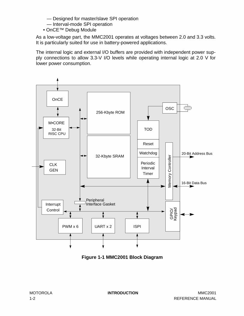
MOTOROLA INTRODUCTION MMC2001 1-2 REFERENCE MANUAL
— Designed for master/slave SPI operation— Interval-mode SPI operation
• OnCE™ Debug Module
As a low-voltage part, the MMC2001 operates at voltages between 2.0 and 3.3 volts.It is particularly suited for use in battery-powered applications.
The internal logic and external I/O buffers are provided with independent power sup-ply connections to allow 3.3-V I/O levels while operating internal logic at 2.0 V forlower power consumption.
Figure 1-1 MMC2001 Block Diagram
M•CORE
32-Bit
32-Kbyte SRAM20-Bit Address Bus
16-Bit Data Bus
Control
CLK
Watchdog
Mem
ory
Con
trol
ler
TOD
Reset
ISPI
OSC256-Kbyte ROM
PeriodicInterval
OnCE
PWM x 6 UART x 2
TimerGEN
GP
IO/
Key
pad
Interrupt
RISC CPU
PeripheralInterface Gasket

MMC2001 INTEGER CPU MOTOROLA REFERENCE MANUAL 2-1
SECTION 2INTEGER CPU
This section gives a short description of the M•CORE CPU features and some basicbus interface information.
2.1 M•CORE Overview
The 32-bit M•CORE microRISC engine represents a new family of Motorola micropro-cessor core products. The processor architecture has been designed for high-perfor-mance and cost-sensitive embedded control applications, with particular emphasison reduced system power consumption. This makes the M•CORE suitable for bat-tery-operated, portable products, as well as for highly integrated parts designed for ahigh temperature environment.
Total system power consumption is dictated by various components in addition to theprocessor core. In particular, memory power consumption (both on-chip and external)is expected to dominate overall power consumption of the core-plus-memory sub-system. With this factor in mind, the instruction set architecture (ISA) for M•COREmakes the trade-off of absolute performance capability versus total energy consump-tion in favor of reducing the overall energy consumption, while maintaining an accept-ably high level of performance at a given clock frequency.
M•CORE is a streamlined execution engine that provides many of the same perfor-mance enhancements as mainstream reduced instruction set computer (RISC)designs. Fixed length instruction encoding and a strict load/store architecture mini-mize control complexity and overhead. The goal of minimizing the overhead of mem-ory system energy consumption is achieved by adopting a (relatively) short 16-bitinstruction encoding. This choice significantly lowers the memory bandwidth neededto sustain a high rate of instruction execution.
Code density statistics for a number of applications show relative code density com-petitive in comparison to complex instruction set computer (CISC) designs, andimplementation statistics show a large reduction in complexity and overhead relativeto a CISC approach.
In addition to substantial cost and performance benefits, M•CORE also offers advan-tages in power consumption and power management. M•CORE minimizes power dis-sipation by using a fully static design, dynamic power management, and low-voltageoperation. The M•CORE automatically powers-down internal functional blocks thatare not needed on a clock-by-clock basis. Power conservation modes are also pro-vided for absolute power conservation on a coarser granularity.
MOTOROLA INTEGER CPU MMC2001 2-2 REFERENCE MANUAL
2.2 Features
The main features of the M•CORE are as follows:
• 32-bit load/store RISC architecture• Fixed 16-bit instruction length• 16-entry, 32-bit general-purpose register file• Efficient 4-stage execution pipeline, hidden from application software• Single-cycle instruction execution for many instructions• Two cycles for taken branches and memory access instructions• Support for byte, halfword, and word memory accesses• Fast interrupt support with 16-entry dedicated alternate register file• Vectored and autovectored interrupt support
2.3 Microarchitecture Summary
The M•CORE instruction execution pipeline consists of the following stages:
• Instruction fetch• Instruction decode/register file read• Execute• Register writeback
These stages operate in an overlapped fashion, allowing single-clock instruction exe-cution for most instructions.
Sixteen general-purpose registers are provided for source operands and instructionresults. Register R15 is used as the link register to hold the return address for sub-routine calls, and register R0 is associated with the current stack pointer value byconvention.
The execution unit consists of a 32-bit arithmetic/logic unit (ALU), a 32-bit barrelshifter, a find-first-one unit (FFO), result feed-forward hardware, and miscellaneoussupport hardware for multiplication and multiple register loads and stores. Arithmeticand logical operations are executed in a single cycle with the exception of the multi-ply, signed divide, and unsigned divide instructions. The multiply instruction is imple-mented with a 2-bit per clock, overlapped-scan, modified Booth algorithm with early-out capability to reduce execution time for operations with small multiplier values. Thesigned divide and unsigned divide instructions also have data-dependent timing. Afind-first-one unit operates in a single clock cycle.
The program counter unit has a PC incrementer and a dedicated branch addressadder to minimize delays during change of flow operations. Branch target addressesare calculated in parallel with branch instruction decode, with a single pipeline bubblefor taken branches and jumps. This results in an execution time of two clocks. Condi-tional branches that are not taken execute in a single clock.
Memory load and store operations are provided for byte, halfword, and word (32-bit)data with automatic zero extension of byte and halfword load data. These instructionscan execute in two clock cycles. Load and store multiple register instructions allowlow overhead context save and restore operations. These instructions can execute in(N+1) clock cycles, where N is the numbers of registers to transfer.
MMC2001 INTEGER CPU MOTOROLA REFERENCE MANUAL 2-3
A single condition code/carry (C) bit is provided for condition testing and for use inimplementing arithmetic and logical operations greater than 32 bits. Typically, the C-bit is set only by explicit test/comparison operations, not as a side-effect of normalinstruction operation. Exceptions to this rule occur for specialized operations forwhich it is desirable to combine condition setting with actual computation.
A 16-entry alternate register file is provided to support low overhead interrupt excep-tion processing. The CPU supports both vectored and autovectored interrupts.
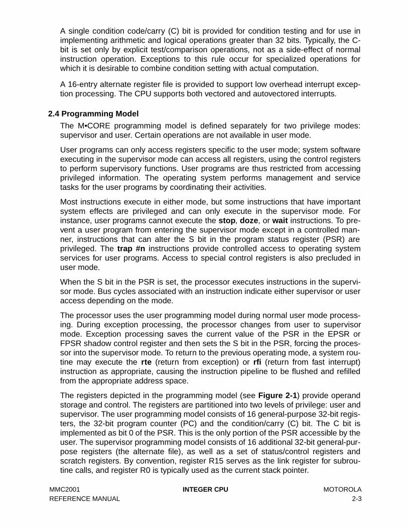
2.4 Programming Model
The M•CORE programming model is defined separately for two privilege modes:supervisor and user. Certain operations are not available in user mode.
User programs can only access registers specific to the user mode; system softwareexecuting in the supervisor mode can access all registers, using the control registersto perform supervisory functions. User programs are thus restricted from accessingprivileged information. The operating system performs management and servicetasks for the user programs by coordinating their activities.
Most instructions execute in either mode, but some instructions that have importantsystem effects are privileged and can only execute in the supervisor mode. Forinstance, user programs cannot execute the stop, doze, or wait instructions. To pre-vent a user program from entering the supervisor mode except in a controlled man-ner, instructions that can alter the S bit in the program status register (PSR) areprivileged. The trap #n instructions provide controlled access to operating systemservices for user programs. Access to special control registers is also precluded inuser mode.
When the S bit in the PSR is set, the processor executes instructions in the supervi-sor mode. Bus cycles associated with an instruction indicate either supervisor or useraccess depending on the mode.
The processor uses the user programming model during normal user mode process-ing. During exception processing, the processor changes from user to supervisormode. Exception processing saves the current value of the PSR in the EPSR orFPSR shadow control register and then sets the S bit in the PSR, forcing the proces-sor into the supervisor mode. To return to the previous operating mode, a system rou-tine may execute the rte (return from exception) or rfi (return from fast interrupt)instruction as appropriate, causing the instruction pipeline to be flushed and refilledfrom the appropriate address space.
The registers depicted in the programming model (see Figure 2-1) provide operandstorage and control. The registers are partitioned into two levels of privilege: user andsupervisor. The user programming model consists of 16 general-purpose 32-bit regis-ters, the 32-bit program counter (PC) and the condition/carry (C) bit. The C bit isimplemented as bit 0 of the PSR. This is the only portion of the PSR accessible by theuser. The supervisor programming model consists of 16 additional 32-bit general-pur-pose registers (the alternate file), as well as a set of status/control registers andscratch registers. By convention, register R15 serves as the link register for subrou-tine calls, and register R0 is typically used as the current stack pointer.
MOTOROLA INTEGER CPU MMC2001 2-4 REFERENCE MANUAL
The alternate file is selected for use via a control bit in the PSR. The status, control,and scratch registers are accessed via the move from control register (mfcr) andmove to control register (mtcr) instructions. When the alternate file is selected via theAF bit in the PSR, general-purpose operands are accessed from it. When the AF bitis cleared, operands are accessed from the normal file. This alternate file is providedto allow very low overhead context switching capability for real-time event handling.
Figure 2-1 Programming Model
The supervisor programming model includes the PSR, which contains operation con-trol and status information. In addition, a set of exception shadow registers is pro-vided to save the state of the PSR and the program counter at the time an exceptionoccurs. A separate set of shadow registers is provided for fast interrupt support tominimize context saving overhead.
Five scratch registers are provided for supervisor software use in handling exceptionevents. A single register is provided to alter the base address of the exception vectortable. Two registers are provided for global control and status.
R0
R1
R2
R3
R4
R5
R6
R7
R8
R9
R12
R13
R14
R15
R11
R10
C
R0’
R1R2R3R4R5R6R7R8R9
R12R13R14R15
R11R10
R0
R1
R2
R3
R4
R5
R6
R7
R8
R9
R12
R13
R14
R15
R11
R10
User Programmer’sModel
Alternate file
Supervisor Programmer’sModel
PCPC
C * bit 0 of PSR
PSR
VBR
EPSR
FPSR
EPC
FPC
SS0
SS1
SS2
CR0
CR1
CR2
CR3
CR4
CR5
CR6
CR7
CR8
CR9
SS4 CR10
GCR CR11
SS3
GSR CR12

MMC2001 INTEGER CPU MOTOROLA REFERENCE MANUAL 2-5
2.5 Data Format Summary
The operand data formats supported by the integer unit are standard two’s-comple-ment data formats. The operand size for each instruction is either explicitly encodedin the instruction (load/store instructions) or implicitly defined by the instruction opera-tion (index operations, byte extraction). Typically, instructions operate on all 32 bits ofthe source operand(s) and generate a 32-bit result.
Memory is viewed from a big-endian byte ordering perspective. The most significantbyte (byte 0) of word 0 is located at address 0. Bits are numbered within a word start-ing with bit 31 as the most significant bit.
Figure 2-2 Data Organization in Memory
Figure 2-3 Data Organization in Registers
Byte 0 Byte 1 Byte 2 Byte 3 Word at 0
31 0
Byte 4 Byte 5 Byte 6 Byte 7 Word at 4
Byte 8 Byte 9 Byte A Byte B Word at 8
Byte C Byte D Byte E Byte F Word at C
Byte Signed ByteSS S S S S S S S S S S S S S S S S S S S S S S S
08 731
Byte Unsigned Byte0 0 0 0 0 0 0 0 0 0 0 0 0 0 0 0 0 0 0 0 0 0 0 0
08 731
Halfword Signed SS S S S S S S S S S S S S S S S
016 1531
Halfword
Halfword Unsigned 0 0 0 0 0 0 0 0 0 0 0 0 0 0 0 0
016 1531
Halfword
031
WordByte 3 Byte 2 Byte 1 Byte 0
MOTOROLA INTEGER CPU MMC2001 2-6 REFERENCE MANUAL
2.6 Operand Addressing Capabilities
M•CORE accesses all memory operands through load and store instructions, trans-ferring data between the general-purpose registers and memory. Register-plus-four-bit scaled displacement addressing mode is used for the load and store instructionsto address byte, halfword, or word (32-bit) data.
Load and store multiple instructions allow a subset of the 16 GPRs to be transferredto or from a base address pointed to by register R0 (the default stack pointer by con-vention).
Load and store register quadrant instructions use register indirect addressing totransfer a register quadrant to or from memory.
2.7 Instruction Set Overview
The instruction set is tailored to support high-level languages and is optimized forthose instructions most commonly executed. A standard set of arithmetic and logicalinstructions is provided, as well as instruction support for bit operations, byte extrac-tion, data movement, control flow modification, and a small set of conditionally exe-cuted instructions which can be useful in eliminating short conditional branches.
Table 2-1 is an alphabetized listing of the M•CORE instruction set. Refer to theM•CORE Reference Manual (MCORERM/AD) for more details on instruction opera-tion.
Table 2-1 M•CORE Instruction Set
Mnemonic Description
ABSADDCADDIADDUANDANDIANDNASRASRC
Absolute ValueAdd with C BitAdd ImmediateAdd UnsignedLogical ANDLogical AND ImmediateAND NOTArithmetic Shift RightArithmetic Shift Right, Update C Bit
BCLRIBFBGENIBGENRBKPTBMASKIBR BREVBSETIBSRBTBTSTI
Bit Clear ImmediateBranch on Condition FalseBit Generate ImmediateBit Generate RegisterBreakpointBit Mask ImmediateBranchBit ReverseBit Set ImmediateBranch to SubroutineBranch on Condition TrueBit Test Immediate

MMC2001 INTEGER CPU MOTOROLA REFERENCE MANUAL 2-7
CLRFCLRTCMPHSCMPLTCMPLTICMPNECMPNEI
Clear Register on Condition FalseClear Register on Condition TrueCompare Higher or SameCompare Less ThanCompare Less Than ImmediateCompare Not EqualCompare Not Equal Immediate
DECFDECGTDECLTDECNEDECTDIVSDIVUDOZE
Decrement on Condition FalseDecrement Register and Set Condition if Result Greater Than ZeroDecrement Register and Set Condition if Result Less Than ZeroDecrement Register and Set Condition if Result Not Equal to ZeroDecrement on Condition TrueDivide Signed IntegerDivide Unsigned IntegerDoze
FF1 Find First One
INCFINCTIXHIXW
Increment on Condition FalseIncrement on Condition TrueIndex HalfwordIndex Word
JMPJMPIJSRJSRI
JumpJump IndirectJump to SubroutineJump to Subroutine Indirect
LD.[BHW]LDMLDQLOOPTLRWLSL, LSRLSLC, LSRCLSLI, LSRI
LoadLoad Multiple RegistersLoad Register QuadrantDecrement with C-Bit Update and Branch if Condition TrueLoad Relative WordLogical Shift Left and RightLogical Shift Left and Right, Update C BitLogical Shift Left and Right by Immediate
MFCRMOVMOVIMOVFMOVTMTCRMULTMVCMVCV
Move from Control RegisterMoveMove ImmediateMove on Condition FalseMove on Condition TrueMove to Control RegisterMultiplyMove C Bit to RegisterMove Inverted C Bit to Register
NOT Logical Complement
OR Logical Inclusive-OR
ROTLIRSUBRSUBIRTERFI
Rotate Left by ImmediateReverse SubtractReverse Subtract ImmediateReturn from ExceptionReturn from Interrupt
Table 2-1 M•CORE Instruction Set (Continued)
Mnemonic Description

MOTOROLA INTEGER CPU MMC2001 2-8 REFERENCE MANUAL
2.8 M•CORE Bus Interface
The M•CORE bus is a synchronous pipelined interface. Signals driven on this bus arerequired to meet the set up and hold time relative to the falling and rising edges of thebus clock.
The M•CORE architecture supports byte, half-word, and word operands, allowingaccess to 8-,16-, and 32-bit data ports through the use of synchronous cycles con-trolled by the size outputs (TSIZ0, TSIZ1).
M•CORE bus interface features are summarized below.
• 32-bit address bus with transfer size indication• 32-bit data bus• Signals referenced to both the rising and falling edges of the bus clock• Only aligned transfers allowed• M•CORE is the only bus master; no arbitration support• 32-bit fixed port size
2.8.1 Bus Characteristics
The bus transfers information between the M•CORE and external memory or aperipheral device via the external and internal bus interfaces. The M•CORE port sizeis fixed at 32 bits. External devices can accept or provide eight or 16 bits in paralleland must follow the handshake protocol described in this section. The number of bitsaccepted or provided during a bus transfer is defined as the transfer size. TheM•CORE uses the address bus to specify the address for the transfer and the databus to transfer the data. Control and attribute signals indicate the beginning and type
SEXTBSEXTHST.[BHW]STMSTQSTOPSUBCSUBUSUBISYNC
Sign-Extend ByteSign-Extend HalfwordStoreStore Multiple RegistersStore Register QuadrantStopSubtract with C BitSubtractSubtract ImmediateSynchronize
TRAPTSTTSTNBZ
TrapTest OperandsTest for No Byte Equal Zero
WAIT Wait
XORXSRXTRB0XTRB1XTRB2XTRB3
Exclusive ORExtended Shift RightExtract Byte 0Extract Byte 1Extract Byte 2Extract Byte 3
ZEXTBZEXTH
Zero-Extend ByteZero-Extend Halfword
Table 2-1 M•CORE Instruction Set (Continued)
Mnemonic Description
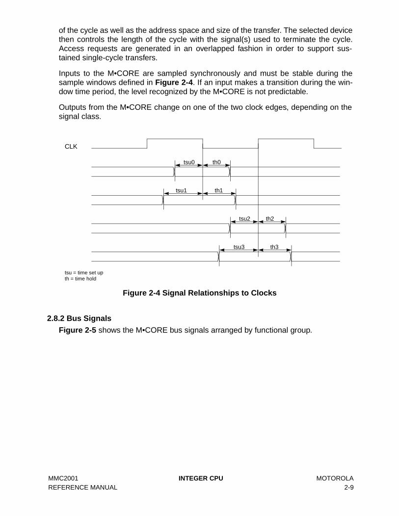
MMC2001 INTEGER CPU MOTOROLA REFERENCE MANUAL 2-9
of the cycle as well as the address space and size of the transfer. The selected devicethen controls the length of the cycle with the signal(s) used to terminate the cycle.Access requests are generated in an overlapped fashion in order to support sus-tained single-cycle transfers.
Inputs to the M•CORE are sampled synchronously and must be stable during thesample windows defined in Figure 2-4. If an input makes a transition during the win-dow time period, the level recognized by the M•CORE is not predictable.
Outputs from the M•CORE change on one of the two clock edges, depending on thesignal class.
Figure 2-4 Signal Relationships to Clocks
2.8.2 Bus Signals
Figure 2-5 shows the M•CORE bus signals arranged by functional group.
CLK
tsu0 th0
tsu1 th1
tsu2 th2
tsu3 th3
tsu = time set upth = time hold
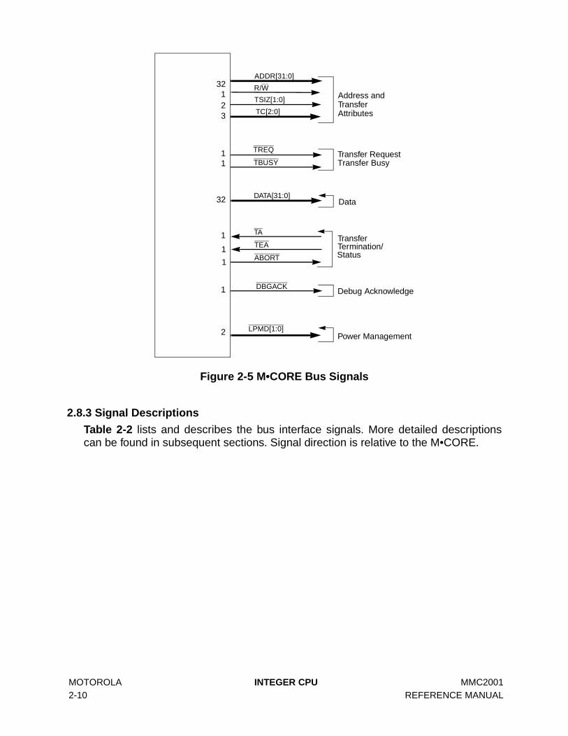
MOTOROLA INTEGER CPU MMC2001 2-10 REFERENCE MANUAL
Figure 2-5 M•CORE Bus Signals
2.8.3 Signal Descriptions
Table 2-2 lists and describes the bus interface signals. More detailed descriptionscan be found in subsequent sections. Signal direction is relative to the M•CORE.
ADDR[31:0]
R/W
TREQ
TSIZ[1:0]
TC[2:0]
TA
DATA[31:0]
TEA
ABORT
321
1
23
1
32
1
1
Address andTransferAttributes
Data
Transfer
StatusTermination/
TBUSY1Transfer RequestTransfer Busy
LPMD[1:0]2 Power Management
DBGACK1 Debug Acknowledge
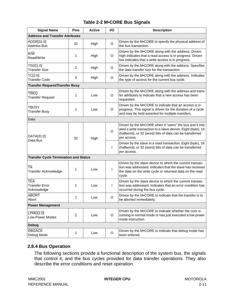
MMC2001 INTEGER CPU MOTOROLA REFERENCE MANUAL 2-11
2.8.4 Bus Operation
The following sections provide a functional description of the system bus, the signalsthat control it, and the bus cycles provided for data transfer operations. They alsodescribe the error conditions and reset operation.
Table 2-2 M•CORE Bus Signals
Signal Name Pins Active I/O Description
Address and Transfer Attributes
ADDR[31:0]Address Bus
32 High ODriven by the M•CORE to specify the physical address of the bus transaction.
R/WRead/Write
1 High ODriven by the M•CORE along with the address. Driven high indicates that a read access is in progress. Driven low indicates that a write access is in progress.
TSIZ[1:0]Transfer Size
2 High ODriven by the M•CORE along with the address. Specifies the data transfer size for the transaction.
TC[2:0]Transfer Code
3 High ODriven by the M•CORE along with the address. Indicates the type of access for the current bus cycle.
Transfer Request/Transfer Busy
TREQTransfer Request
1 Low ODriven by the M•CORE along with the address and trans-fer attributes to indicate that a new access has been requested.
TBUSYTransfer Busy
1 Low ODriven by the M•CORE to indicate that an access is in progress. This signal is driven for the duration of a cycle and may be held asserted for multiple transfers.
Data
DATA[31:0]Data Bus
32 High
O
Driven by the M•CORE when it “owns” the bus and it initi-ated a write transaction to a slave device. Eight (byte), 16 (halfword), or 32 (word) bits of data can be transferred per access.
IDriven by the slave in a read transaction. Eight (byte), 16 (halfword), or 32 (word) bits of data can be transferred per access.
Transfer Cycle Termination and Status
TATransfer Acknowledge
1 Low I
Driven by the slave device to which the current transac-tion was addressed. Indicates that the slave has received the data on the write cycle or returned data on the read cycle.
TEATransfer Error Acknowledge
1 Low IDriven by the slave device to which the current transac-tion was addressed. Indicates that an error condition has occurred during the bus cycle.
ABORTAbort
1 Low ODriven by the M•CORE to indicate that the transfer is to be aborted immediately.
Power Management
LPMD[1:0]Low-Power Modes
2 Low ODriven by the M•CORE to indicate whether the core is running in normal mode or has just executed a low power mode instruction.
Debug
DBGACKDebug Mode
1 Low ODriven by the M•CORE to indicate that debug mode has been entered.

MOTOROLA INTEGER CPU MMC2001 2-12 REFERENCE MANUAL
The M•CORE receives a clock input (CLK) from an external clock source and gener-ates two internal clocks (C1 and C2). The CLK input sets the frequency of operationfor the bus interface directly. The clock source monitors the M•CORE low power modeoutputs (LPMD[1:0]) and controls the clock input to the M•CORE accordingly by forc-ing the clocks low for low-power operation.
Data transfers occur between an internal register and the external bus. The internalregister connects to the external data bus through the internal data bus and a datamultiplexer. The data multiplexer establishes the necessary connections for differentcombinations of address and data sizes. This multiplexer is physically positioned inthe overall system to minimize power consumption by minimizing loading and reduc-ing unnecessary signal transitions. Logically, however, it is considered part of theM•CORE.
The M•CORE does not support dynamic bus sizing and expects the referenceddevice to accept the requested access width. Peripherals with an interface width of Nbits should not define internal registers greater than N bits wide.
Misaligned transfers are not supported. The M•CORE interface may drive theADDR[1:0] address lines to a value which is not representative of an aligned transfer,but expects aligned data to be transferred. ADDR[1:0] should be selectively ignoredby external logic, depending on the size of the transfer.
The data multiplexer takes the four bytes of the core interface data bus and routesthem to their required positions to interface properly to memory or peripherals. Theexternal multiplexer connections to memory are controlled on a byte granularity andare referred to as MB0–MB3, where MB0 resides at byte address 0 (mod 4) and MB3resides at byte address 3 (mod 4). For example, MB0 would normally be routed toDATA[31:24] on a word transfer, but it can also be routed to DATA[7:0] for supporting abyte data transfer. The same is true for any of the other operand bytes.
Figure 2-6 shows the connection requirements for the multiplexer. The transfer size(TSIZ[1:0]) and byte offset (ADDR1 and ADDR0) signals determine the positioning ofthe bytes (see Table 2-3).
Table 2-3 Interface Requirements for Read and Write Cycles
Transfer Size
Active Interface Bus Sections Mux ConnectionsTSIZ1 TSIZ0 ADDR1 ADDR0 DATA[31:24] DATA[23:16] DATA[15:8] DATA[7:0]
Byte
0000
1111
0011
0101
————
————
————
MB0MB1MB2MB3
abcd
Halfword11
00
01
XX
——
——
MB0MB2
MB1MB3
ef
Word 0 0 X X MB0 MB1 MB2 MB3 g
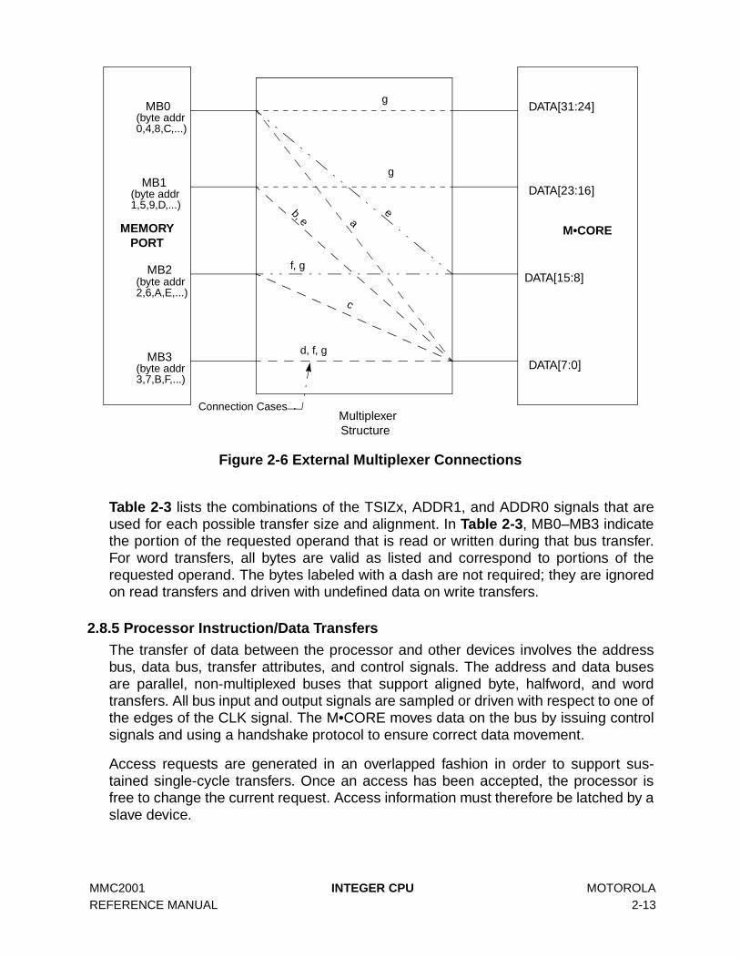
MMC2001 INTEGER CPU MOTOROLA REFERENCE MANUAL 2-13
Figure 2-6 External Multiplexer Connections
Table 2-3 lists the combinations of the TSIZx, ADDR1, and ADDR0 signals that areused for each possible transfer size and alignment. In Table 2-3, MB0–MB3 indicatethe portion of the requested operand that is read or written during that bus transfer.For word transfers, all bytes are valid as listed and correspond to portions of therequested operand. The bytes labeled with a dash are not required; they are ignoredon read transfers and driven with undefined data on write transfers.
2.8.5 Processor Instruction/Data Transfers
The transfer of data between the processor and other devices involves the addressbus, data bus, transfer attributes, and control signals. The address and data busesare parallel, non-multiplexed buses that support aligned byte, halfword, and wordtransfers. All bus input and output signals are sampled or driven with respect to one ofthe edges of the CLK signal. The M•CORE moves data on the bus by issuing controlsignals and using a handshake protocol to ensure correct data movement.
Access requests are generated in an overlapped fashion in order to support sus-tained single-cycle transfers. Once an access has been accepted, the processor isfree to change the current request. Access information must therefore be latched by aslave device.
M•CORE
DATA[31:24]
DATA[23:16]
DATA[15:8]
DATA[7:0]
MB0
MB1
MB2
MB3
MEMORYPORT
MultiplexerStructure
(byte addr0,4,8,C,...)
(byte addr3,7,B,F,...)
(byte addr2,6,A,E,...)
(byte addr1,5,9,D,...)
g
g
b, e ae
c
f, g
d, f, g
Connection Cases

MOTOROLA INTEGER CPU MMC2001 2-14 REFERENCE MANUAL
2.8.6 Bus Exception Cycles
The M•CORE bus interface requires assertion of TA from an external device to signalthat a bus cycle is complete. External circuitry can provide TEA when no deviceresponds to indicate that an error condition is associated with an access. This allowsthe cycle to terminate and the processor to enter exception processing for the errorcondition if appropriate.
To control termination of a bus cycle for a bus error condition properly, TA and TEAmust be asserted and negated about the same rising edge of CLK.
The system hardware can use the TEA signal to abort the current bus cycle when afault is detected. When the processor recognizes a bus error condition for an access,the access is terminated immediately.
When a bus cycle is terminated with a bus error, the M•CORE can enter access errorexception processing immediately following the bus cycle, or it can defer processingthe exception. The instruction pre-fetch mechanism requests instruction words fromthe instruction memory unit before it is ready to execute them. If a bus error occurs onan instruction fetch, the processor does not take the exception until it attempts to usethe instruction. If an intervening instruction causes a branch or if a task switch occurs,the access error exception for the unused access does not occur.
A bus error termination for any write or read access that references data specificallyrequested by the execution unit causes the processor to begin exception processingimmediately.
Table 2-4 Termination Result Summary
TA TEA Result
Don’t Care Low Bus Error — terminate and take bus error exception if appropriate
Low High Normal cycle terminate and continue
High High Insert wait states
MMC2001 SYSTEM MEMORY MAP MOTOROLA REFERENCE MANUAL 3-1
SECTION 3SYSTEM MEMORY MAP
3.1 Overview
This section describes the address allocation conventions for the MMC2001 system.
The general address map shown in Table 3-1 is recommended for all members of theMMC2001 architecture. Accesses to unimplemented regions of the map may result inTEA termination to the processor.
For the initial implementations of MMC2001, the address range of 0x4000 0000 –
0xFFFF FFFF is reserved for future use. Accesses to this range result in a transfererror termination to the CPU.
Note that in the current MMC2001 implementation, accesses to on-chip devices otherthan RAM and ROM are considered privileged; no user mode access is allowed toon-chip peripherals.
3.2 Peripheral Module Address Allocation
The register blocks for all on-chip peripheral devices are located on 4096-byte bound-aries. Peripherals that require additional address space (e.g., for buffers) areassigned additional 4-Kbyte blocks. In this case, peripherals are located on a 2n
address boundary corresponding to the size of the block. Within a 4-Kbyte block,peripheral registers may be incompletely decoded, such that the register map repeatsthroughout the entire block; or the peripheral may return undefined values for unim-plemented register addresses. The description of the peripherals in this documentprovide information regarding the result of accesses to unimplemented registers.
Table 3-1 MMC2001 Module Address Map
Address Range UseSupervisor
AccessUser Access
00000000 – 00000003Off-chip boot ROM vector fetch (MOD asserted)
Full
—
00000004 – 0FFFFFFF On-chip ROM Selective
10000000 – 1FFFFFFF On-chip peripherals None
20000000 – 2FFFFFFF Off-chip devices Selective
30000000 – 3FFFFFFF On-chip RAM Selective
40000000 – FFFFFFFF Reserved —
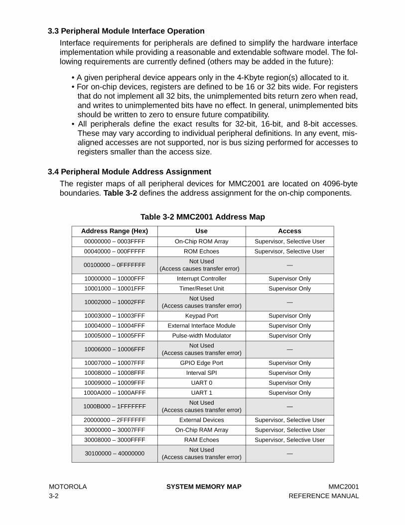
MOTOROLA SYSTEM MEMORY MAP MMC2001 3-2 REFERENCE MANUAL
3.3 Peripheral Module Interface Operation
Interface requirements for peripherals are defined to simplify the hardware interfaceimplementation while providing a reasonable and extendable software model. The fol-lowing requirements are currently defined (others may be added in the future):
• A given peripheral device appears only in the 4-Kbyte region(s) allocated to it.• For on-chip devices, registers are defined to be 16 or 32 bits wide. For registers
that do not implement all 32 bits, the unimplemented bits return zero when read,and writes to unimplemented bits have no effect. In general, unimplemented bitsshould be written to zero to ensure future compatibility.
• All peripherals define the exact results for 32-bit, 16-bit, and 8-bit accesses.These may vary according to individual peripheral definitions. In any event, mis-aligned accesses are not supported, nor is bus sizing performed for accesses toregisters smaller than the access size.
3.4 Peripheral Module Address Assignment
The register maps of all peripheral devices for MMC2001 are located on 4096-byteboundaries. Table 3-2 defines the address assignment for the on-chip components.
Table 3-2 MMC2001 Address Map
Address Range (Hex) Use Access
00000000 – 0003FFFF On-Chip ROM Array Supervisor, Selective User
00040000 – 000FFFFF ROM Echoes Supervisor, Selective User
00100000 – 0FFFFFFFNot Used
(Access causes transfer error)—
10000000 – 10000FFF Interrupt Controller Supervisor Only
10001000 – 10001FFF Timer/Reset Unit Supervisor Only
10002000 – 10002FFFNot Used
(Access causes transfer error)—
10003000 – 10003FFF Keypad Port Supervisor Only
10004000 – 10004FFF External Interface Module Supervisor Only
10005000 – 10005FFF Pulse-width Modulator Supervisor Only
10006000 – 10006FFFNot Used
(Access causes transfer error)—
10007000 – 10007FFF GPIO Edge Port Supervisor Only
10008000 – 10008FFF Interval SPI Supervisor Only
10009000 – 10009FFF UART 0 Supervisor Only
1000A000 – 1000AFFF UART 1 Supervisor Only
1000B000 – 1FFFFFFFNot Used
(Access causes transfer error)—
20000000 – 2FFFFFFF External Devices Supervisor, Selective User
30000000 – 30007FFF On-Chip RAM Array Supervisor, Selective User
30008000 – 3000FFFF RAM Echoes Supervisor, Selective User
30100000 – 40000000Not Used
(Access causes transfer error)—

MMC2001 SIGNAL DESCRIPTIONS MOTOROLA REFERENCE MANUAL 4-1
SECTION 4SIGNAL DESCRIPTIONS
4.1 Overview
This section contains brief descriptions of MMC2001 signal and power connections.Specific details of signal operation are provided in the individual module descriptions.Figure 4-1 shows MMC2001 signals by functional group.
Figure 4-1 Functional Signal Groups
KPP
INT[7:0]Edge
ADDR[19:0]
DATA[15:0]
CLKGEN
XOSCXTALOSC/
EXOSC
TMSTDIOnCETDO
TCK
TxD1/TSIZ0RxD1/TSIZ1
EB0
R/WOE
EB1
MO
D
CLKOUT
CPU
Peripheral
SRAM
TE
ST
PWM
CLKIN
ROW[7:0]COL[7:0]CTS0/PSTAT3
RTS0/PSTAT2
ISPI
SP
I_M
ISO
S
PI_
MO
SI
SP
I_E
N
SP
I_C
LK
Port
PWM[5:0]
TxD0/PSTAT0RxD0/PSTAT1
TR
ST
DE
VSTBY VBATT
CS[2:0],CS3
SP
I_G
P
Timer/ResetModule
RS
TIN
LVR
ST
IN
RS
TOU
T
STBY
UART1
UART0
ROM
EIM
Interface Gasket

MOTOROLA SIGNAL DESCRIPTIONS MMC2001 4-2 REFERENCE MANUAL
4.2 Signal Index
Table 4-1 Pin Requirements in 144-Pin Package
Name Alt Qty Dir Pull-Up1 Reset2 Use
External Bus
ADDR[19:0] — 20 O — OL Address bus
DATA[15:0] — 16 I/O Keeper I Data bus
R/W — 1 O — H Read/write enable
EB0 — 1 O — H Enable data bus byte 0 (DATA[15:8])
EB1 — 1 O — H Enable data bus byte 1 (DATA[7:0])
OE — 1 O — H Output enable
Chip Selects
CS0 — 1 O — CS0 Chip select for external Flash
CS1 GPO 1 O — GPOH Chip select for external RAM
CS2 GPO 1 O — GPOH Chip select (spare)
CS3 GPO 1 O — GPOL Chip select for external LCD
Clock, Reset, and Miscellaneous
CLKIN — 1 I — — Programmable clock input
CLKOUT — 1 O — OL Programmable clock output
XOSC — 1 O — — 32.768-kHz XTAL output
EXOSC — 1 I — — 32.768-kHz XTAL input
MOD — 1 I — — Boot ROM control
RSTOUT — 1 O — — Resets external components
RSTIN — 1 I — — Initiates system reset
LVRSTIN — 1 I — — Low voltage supply switching control
Debug and Test Port Control
TMS — 1 I 47-K pull-up — Test mode select
TDI — 1 I 47-K pull-up — Test data input
TDO — 1 O — — Test data output
TCK — 1 I 47-K pull-up — Test clock input
TRST — 1 I 47-K pull-up — Initiates test controller reset
DE — 1 I/O 47-K pull-up — Initiates or acknowledges debug mode entry
TEST — 1 I 100-K pulldown — Factory test mode
Keypad and Edge Port
COL[7:0] GPIO 8 I/O — GPI Column 7 – 0
ROW[7:0] GPIO 8 I/O 47-K pull-up GPI Row 7 – 0
INT[7:0] GPIO 8 I/O — GPI External interrupts 7 – 0
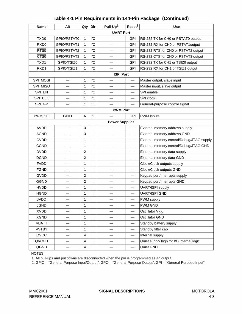
MMC2001 SIGNAL DESCRIPTIONS MOTOROLA REFERENCE MANUAL 4-3
UART Port
TXD0 GPIO/PSTAT0 1 I/O — GPI RS-232 TX for CH0 or PSTAT0 output
RXD0 GPIO/PSTAT1 1 I/O — GPI RS-232 RX for CH0 or PSTAT1output
RTS0 GPIO/PSTAT2 1 I/O — GPI RS-232 RTS for CH0 or PSTAT2 output
CTS0 GPIO/PSTAT3 1 I/O — GPI RS-232 CTS for CH0 or PSTAT3 output
TXD1 GPIO/TSIZ0 1 I/O — GPI RS-232 TX for CH1 or TSIZ0 output
RXD1 GPIO/TSIZ1 1 I/O — GPI RS-232 RX for CH1 or TSIZ1 output
ISPI Port
SPI_MOSI — 1 I/O — — Master output, slave input
SPI_MISO — 1 I/O — — Master input, slave output
SPI_EN — 1 I/O — — SPI enable
SPI_CLK — 1 I/O — — SPI clock
SPI_GP — 1 O — — General-purpose control signal
PWM Port
PWM[5:0] GPIO 6 I/O — GPI PWM inputs
Power Supplies
AVDD — 3 I — — External memory address supply
AGND — 3 I — — External memory address GND
CVDD — 1 I — — External memory control/Debug/JTAG supply
CGND — 1 I — — External memory control/Debug/JTAG GND
DVDD — 2 I — — External memory data supply
DGND — 2 I — — External memory data GND
FVDD — 1 I — — Clock/Clock outputs supply
FGND — 1 I — — Clock/Clock outputs GND
GVDD — 2 I — — Keypad port/Interrupts supply
GGND — 2 I — — Keypad port/Interrupts GND
HVDD — 1 I — — UART/ISPI supply
HGND — 1 I — — UART/ISPI GND
JVDD — 1 I — — PWM supply
JGND — 1 I — — PWM GND
XVDD — 1 I — — Oscillator VDD
XGND — 1 I — — Oscillator GND
VBATT — 1 I — — Standby battery supply
VSTBY — 1 I — — Standby filter cap
QVCC — 4 I — — Internal supply
QVCCH — 4 I — — Quiet supply high for I/O internal logic
QGND — 4 I — — Quiet GND
NOTES:1. All pull-ups and pulldowns are disconnected when the pin is programmed as an output.2. GPIO = “General-Purpose Input/Output”, GPO = “General-Purpose Output”, GPI = “General-Purpose Input”.
Table 4-1 Pin Requirements in 144-Pin Package (Continued)
Name Alt Qty Dir Pull-Up1 Reset2 Use
MOTOROLA SIGNAL DESCRIPTIONS MMC2001 4-4 REFERENCE MANUAL
4.3 Bus Signals
This section describes the interface signals for external memory and peripherals.
4.3.1 Address Bus (ADDR[19:0])
The output address bus pins are used to address external devices. To minimizepower dissipation, they do not change state unless external memory is beingaccessed.
4.3.2 Data Bus (DATA[15:0])
These pins provide the bidirectional data bus for external memory accesses.DATA[15:0] are held in their previous logic state when there is no external bus activity.This is accomplished with weak “keepers” inside the I/O buffers. They are also kept intheir previous state during hardware reset.
4.3.3 Output Enable (OE)
This active-low output signal indicates the bus access is a read and enables slavedevices to drive the data bus.
4.3.4 Read/Write Enable (R/W)
This active-low output signal indicates whether the current bus access is a read orwrite.
4.3.5 Enable Byte 1 (EB1)
This active-low output pin is active during an operation to data bits DATA[7:0]. It maybe configured to assert for both read and write cycles, or for write cycles only.
4.3.6 Enable Byte 0 (EB0)
This active-low output pin is active during an operation to data bits DATA[15:8]. It maybe configured to assert for both read and write cycles, or for write cycles only.
4.3.7 Chip Selects (CS3, CS[2:0])
These output pins provide chip selects to external devices.
4.3.8 Internal ROM Disable (MOD)
This active-low input pin provides the capability of disabling the on-chip ROM andforcing CS0 to be used to select an external boot ROM.
4.4 Exception Control Signals
4.4.1 Reset (RSTIN)
This active-low input signal is used to initiate a system reset. An external reset signalresets the MMC2001 and most internal peripherals. The debug module is unaffectedby RSTIN; this function is provided through the TRST pin.
MMC2001 SIGNAL DESCRIPTIONS MOTOROLA REFERENCE MANUAL 4-5
4.4.2 Low Voltage Reset (LVRSTIN)
This active-low input signal is used to initiate a system reset and to cause the backuppower supply source to be selected for the RAM array and the OSC/time-of-day timer.This external reset signal resets the MMC2001 and most internal peripherals. Thedebug module is unaffected by LVRSTIN; this function is provided through the TRSTpin.
4.4.3 Reset Out (RSTOUT)
This active-low output signal is used to reset external components. This pin isasserted when any internal reset source is active.
4.5 Clock Signals
These signals are used by the MMC2001 for controlling or generating the systemclocks. See SECTION 8 CLOCK MODULE AND LOW-POWER MODES for moreinformation on the various clocking methods and frequencies.
4.5.1 Crystal Oscillator (XOSC, EXOSC)
These pins are the connections for an external crystal to the internal oscillator circuitfor generation of the internal LOW_REFCLK. EXOSC is the input pin, and XOSC isthe output.
4.5.2 Clock Input (CLKIN)
This input pin provides the HI_REFCLK clock source to the CPU and internal periph-erals.
4.5.3 Clock Output (CLKOUT)
This output pin provides an external clock source, either the LO_REFCLK or theHI_REFCLK.
4.6 Debug and Emulation Support Signals
These signals are used for testing or serial debugging. See SECTION 16 OnCE™DEBUG MODULE for more information on these signals and debug mode.
4.6.1 Test Clock (TCK)
The test clock input (TCK) pin is the test clock used to synchronize the JTAG testlogic. The TCK pin has an internal 47-Kbyte pull-up resistor.
4.6.2 Test Data Input (TDI)
The test data input (TDI) pin is the serial input for test instructions and data. TDI issampled on the rising edge of TCK and it has an internal 47-Kbyte pull-up resistor.
MOTOROLA SIGNAL DESCRIPTIONS MMC2001 4-6 REFERENCE MANUAL
4.6.3 Test Data Output (TDO)
The test data output (TDO) pin is the serial output for test instructions and data. TDOis three-stateable and is actively driven in the shift-IR and shift-DR controller states.TDO changes on the falling edge of TCK.
4.6.4 Test Mode Select (TMS)
The test mode select input (TMS) pin is used to sequence the test controller’s statemachine. The TMS is sampled on the rising edge of TCK. It has an internal 47-Kbytepull-up resistor.
4.6.5 Test Reset (TRST)
The active-low Schmitt trigger input pin TRST is used to initialize the test controllerasynchronously. The TRST pin has an internal 47-Kbyte pull-up resistor.
4.6.6 Debug Event (DE)
DE is an open drain, bidirectional, active low pin. As an input, it provides a means ofentering debug mode from an external command controller. As an output, it providesa means of acknowledging that the CPU has entered debug mode.
This pin, when asserted as an input, causes the CPU to finish the current instructionbeing executed, save the instruction pipeline information, enter debug mode, and waitfor commands to be entered from the serial debug input line. This pin is asserted asan output for several clock cycles when the CPU enters debug mode as a result of adebug request or as a result of meeting a breakpoint condition.
If used to enter debug mode, DE must be negated after the OnCE responds with anacknowledge and before sending the first OnCE command. The DE pin has an inter-nal 47-Kbyte pull-up resistor.
4.6.7 Factory Test Mode (TEST)
This input is used to select factory test mode. A description of the functionality of thispin is detailed in the factory test document. The TEST pin has an internal 100-Kbytepulldown resistor.
4.7 External Interrupts/GPIO Signals
These pins provide the software with general-purpose access external to the chip.See SECTION 13 EXTERNAL INTERRUPTS/GPIO (EDGE PORT) for more informa-tion on these signals.
4.7.1 External Interrupts 7 – 0 (INT[7:0])
These bidirectional pins comprise the external interface to the GPIO module.
MMC2001 SIGNAL DESCRIPTIONS MOTOROLA REFERENCE MANUAL 4-7
4.8 Keypad Signals
4.8.1 Column Strobes (COL[7:0])
These are general-purpose I/O pins used as keypad column strobes. They are open-drain selectable in software. The default state at reset is general-purpose input.
4.8.2 Row Senses (ROW[7:0])
These are general-purpose I/O pins used as keypad row senses. The default state atreset is general-purpose input. On-chip 47-Kbyte pull-up resistors are connected tothese pins.
4.9 UART Module Signals
The following signals are used by the UART module for data and clock signals. Theyare also shared for provision of internal processor status. See SECTION 11 UNIVER-SAL ASYNCHRONOUS RECEIVER/TRANSMITTER MODULE for more informationon these signals. See 7.7 EIM Configuration Register for provision of internal statussignal operation.
4.9.1 Receive Data (RxD0, RxD1)
These signals are used for receiver data input for UART channels 0 and 1, respec-tively. Data is sampled on the rising edge of the clock source, with the least significantbit received first.
RxD0 is used to provide the PSTAT1 internal status signal when the PSTEN bit in theEIM configuration register is set. In this case it operates as an active-high PSTAT1output.
RxD1 is used to provide the TSIZ1 internal status signal when the SZEN bit in theEIM configuration register is set. In this case it operates as an active-high TSIZ1 out-put.
4.9.2 Transmit Data (TxD0, TxD1)
These signals are used for transmit data output for UART channels 0 and 1, respec-tively. The output is held high (“mark” condition) when the transmitter is disabled, idle,or operating in the local loopback mode. Data is shifted out at the falling edge of theclock source with the least significant bit transmitted first.
TxD0 is used to provide the PSTAT0 internal status signal when the PSTEN bit in theEIM configuration register is set. In this case it operates as an active-high PSTAT0output.
TxD1 is used to provide the TSIZ0 internal status signal when the SZEN bit in theEIM configuration register is set. In this case it operates as an active-high TSIZ0 out-put.

MOTOROLA SIGNAL DESCRIPTIONS MMC2001 4-8 REFERENCE MANUAL
4.9.3 Clear to Send (CTS0)
This active-low signal can be programmed as the clear-to-send output for UARTchannel 0.
CTS0 is used to provide the PSTAT3 internal status signal when the PSTEN bit in theEIM configuration register is set. In this case it operates as an active-high PSTAT3output.
4.9.4 Request to Send (RTS0)
This active-low signal can be programmed as the request-to-send input for UARTchannel 0.
RTS0 is used to provide the PSTAT2 internal status signal when the PSTEN bit in theEIM configuration register is set. In this case it operates as an active-high PSTAT2output.
4.10 Serial Peripheral Interface Module Signals
The following signals are used by the serial peripheral module. See SECTION 12INTERVAL MODE SERIAL PERIPHERAL INTERFACE for more information onthese signals.
4.10.1 SPI Data Master Out/Slave In (SPI_MOSI)
This signal is the serial data output from the SPI in master mode and the serial datainput in slave mode.
4.10.2 SPI Data Master In/Slave Out (SPI_MISO)
This signal is the serial data input to the ISPI in master mode and the serial data out-put in slave mode.
4.10.3 SPI Serial Clock (SPI_CLK)
This I/O signal is the serial shift clock for the SPI.
4.10.4 SPI Enable (SPI _EN)
This I/O signal is the peripheral chip select pin in master mode and is a slave enablein slave mode.
4.10.5 SPI General-Purpose Output (SPI _GP)
This output signal is used as a general-purpose control signal for external logic ordevices.
4.11 Pulse Width Modulator Signals
See SECTION 15 PULSE WIDTH MODULATOR for more information on these sig-nals.

MMC2001 SIGNAL DESCRIPTIONS MOTOROLA REFERENCE MANUAL 4-9
4.11.1 PWM[5:0]
These pins provide the external interface to the PWM block. They may be configuredas general-purpose I/O if the PWM output function is not needed. The default state atreset is general-purpose input.
4.12 Power and Ground Pins
These pins provide system power and ground to the MMC2001. Multiple pins are pro-vided for adequate current capability. All power supply pins must have adequatebypass capacitance for high-frequency noise suppression.
4.12.1 Positive Supply (VDD) This pin supplies positive power to the chip.
4.12.2 Ground (GND)
This pin is the negative supply (ground) to the chip.
4.12.3 Standby Battery Power (VBATT)
This pin supplies positive battery standby power to the chip.
4.12.4 Standby Power Filter (VSTBY)
This pin is used to provide an external filter capacitor connection for the standby volt-age switching logic.

MOTOROLA SIGNAL DESCRIPTIONS MMC2001 4-10 REFERENCE MANUAL
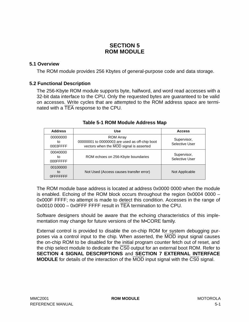
MMC2001 ROM MODULE MOTOROLA REFERENCE MANUAL 5-1
SECTION 5ROM MODULE
5.1 Overview
The ROM module provides 256 Kbytes of general-purpose code and data storage.
5.2 Functional Description
The 256-Kbyte ROM module supports byte, halfword, and word read accesses with a32-bit data interface to the CPU. Only the requested bytes are guaranteed to be validon accesses. Write cycles that are attempted to the ROM address space are termi-nated with a TEA response to the CPU.
The ROM module base address is located at address 0x0000 0000 when the moduleis enabled. Echoing of the ROM block occurs throughout the region 0x0004 0000 –0x000F FFFF; no attempt is made to detect this condition. Accesses in the range of0x0010 0000 – 0x0FFF FFFF result in TEA termination to the CPU.
Software designers should be aware that the echoing characteristics of this imple-mentation may change for future versions of the M•CORE family.
External control is provided to disable the on-chip ROM for system debugging pur-poses via a control input to the chip. When asserted, the MOD input signal causesthe on-chip ROM to be disabled for the initial program counter fetch out of reset, andthe chip select module to dedicate the CS0 output for an external boot ROM. Refer toSECTION 4 SIGNAL DESCRIPTIONS and SECTION 7 EXTERNAL INTERFACEMODULE for details of the interaction of the MOD input signal with the CS0 signal.
Table 5-1 ROM Module Address Map
Address Use Access
00000000to
0003FFFF
ROM Array00000001 to 00000003 are used as off-chip boot
vectors when the MOD signal is asserted
Supervisor, Selective User
00040000to
000FFFFFROM echoes on 256-Kbyte boundaries
Supervisor, Selective User
00100000to
0FFFFFFFNot Used (Access causes transfer error) Not Applicable
MOTOROLA ROM MODULE MMC2001 5-2 REFERENCE MANUAL
The SPROM control bit in the EIM configuration register allows selective access pro-tection to be applied to the ROM. (See 7.7 EIM Configuration Register.) This bitmay be used to control read access to the ROM based on the state of the M•COREPSR(S) bit. Attempted cycles to a protected ROM address space are terminated witha TEA response to the CPU.
5.3 Applications
The ROM module can be used to store:
• Reset boot code• Frequently accessed code• Table of constants• Revision and identification registers for all MMC2001 peripherals• Self-test diagnostic code

MMC2001 STATIC RAM MODULE MOTOROLA REFERENCE MANUAL 6-1
SECTION 6STATIC RAM MODULE
6.1 Overview
The static RAM (SRAM) module provides 32 Kbytes of general-purpose code anddata storage.
6.2 Functional Description
The 32-Kbyte SRAM module supports byte, halfword, and word accesses with a 32-bit data interface to the CPU. Only the requested bytes are guaranteed to be valid onread accesses. The SRAM acknowledges all accesses to its memory space.
The SRAM module occupies physical addresses 0x3000 0000 – 0x3000 7FFF. Echo-ing of the SRAM block occurs throughout the region 0x3000 8000 – 0x300F FFFF; noattempt is made to detect this condition. Accesses in the range of 0x3010 0000 –0x3FFF FFFF result in TEA termination to the CPU.
Software designers should be aware that the echoing characteristics of this imple-mentation may change for future versions of the M•CORE family.
The SPRAM control bit in the EIM configuration register allows selective access pro-tection to be applied to the RAM. (See 7.7 EIM Configuration Register.) This bitmay be used to control access to the RAM based on the state of the M•COREPSR(S) bit. Attempted cycles to a protected RAM address space are terminated witha TEA response to the CPU.
The SRAM module is partitioned into two independent blocks for the purposes of bat-tery backup. An external standby power pin is provided to power both sections of theSRAM for data retention.
The SRAM contents are undefined immediately following a power-on reset.
Table 6-1 Static RAM Module Address Map
Address Use Access
30000000to
30007FFFRAM Array
Supervisor, Selective User
30008000to
3000FFFFRAM Echoes on 32-Kbyte Boundaries
Supervisor, Selective User
30100000to
40000000Not Used (Access causes transfer error) Not Applicable

MOTOROLA STATIC RAM MODULE MMC2001 6-2 REFERENCE MANUAL

MMC2001 EXTERNAL INTERFACE MODULE MOTOROLA REFERENCE MANUAL 7-1
SECTION 7EXTERNAL INTERFACE MODULE
7.1 Overview
The external interface module (EIM) handles the interface to devices external to theMMC2001, including generation of chip selects for external peripherals and memory.It provides the following features:
• Four chip selects for external devices, each covering a range of 16 Mbytes• Programmable wait-state generator for each chip select• Selectable protection for each chip select• Programmable data port size for each chip select• Control for external/internal boot ROM device selection• Bus watchdog counter for all bus cycles• Programmable general output capability for unused chip select outputs• Show cycles to allow internal bus cycles to be monitored externally
Figure 7-1 EIM Block Diagram
7.2 Signals
7.2.1 Address Bus
The ADDR[19:0] signals are address bus outputs used to address external devices.
Inte
rnal
Bus
CS0CS1CS2CS3
TA, TEA
DATA[31:0]
ADDR[31:0], R/W, TSIZ, TC
ADDR[19:0]
EB[0:1]
OE
R/W
DATA[15:0]
MOD
TREQ, TBUSY, ABORT
MODModuleTimer/Reset
EIM
MOTOROLA EXTERNAL INTERFACE MODULE MMC2001 7-2 REFERENCE MANUAL
7.2.2 Data Bus
The DATA[15:0] signals are bidirectional data bus pins used to transfer data betweenthe chip and an external device.
7.2.3 Read/Write
The R/W output signal indicates whether the current bus access is a read or writecycle. A high (logic one) level indicates a read cycle, and a low (logic zero) level indi-cates a write cycle.
7.2.4 Control Signals
The OE and EB[0:1] signals are used to control the interface to the data bus.
7.2.4.1 Output Enable (OE)
This active-low output signal indicates the bus access is a read and enables slavedevices to drive the data bus with read data.
7.2.4.2 Enable Byte 0–1 (EB[0:1] )
These active-low output pins indicate active data bytes for the current access. Theycan be programmed in the chip-select control registers to assert for read and writecycles or for write cycles only. EB0 corresponds to DATA[15:8], and EB1 correspondsto DATA[7:0].
7.2.5 Boot Mode
The MOD input pin selects the initial CPU boot mode during hardware reset.
If this pin is driven to a logic-low level four LOW_REFCLK clock cycles beforeRSTOUT negation, then the internal ROM will be disabled and the CPU will fetch thefirst word from offset 0x0 of the external Flash memory, which is located at the abso-lute address 0x2D00000 in the CPU address space. The internal ROM is disabled forthe first CPU cycle only and is available for subsequent accesses.
If this pin is driven to a logic-high level four LOW_REFCLK clock cycles beforeRSTOUT negation, then the internal ROM is enabled and the CPU fetches the firstword from absolute address 0x0, which is the starting address of the internal ROM.This signal is latched in the timer/reset module, and an internal version is supplied tothe EIM.
7.2.6 Chip Select Outputs
7.2.6.1 Chip Select 0 (CS0 )
This active-low output signal is asserted based on a decode of bits ADDR[31:24] ofthe access address, and at reset based on the value of the MOD input.

MMC2001 EXTERNAL INTERFACE MODULE MOTOROLA REFERENCE MANUAL 7-3
If MOD is driven to a logic-low level four LOW_REFCLK clock cycles before RSTOUTnegation, and the CSEN0 bit is enabled (the default state on reset), then the internalROM is disabled, and CS0 is asserted for the first CPU access. The internal ROM isdisabled for the first CPU access only and is available for subsequent accesses. TheCS0 access uses default values of 15 wait states and a 16-bit port size.
7.2.6.2 Chip Select 1–2 (CS[1:2] )
These active-low output signals are asserted based on a decode of bits ADDR[31:24]of the access address. When disabled, these pins can be used as programmablegeneral-purpose outputs.
7.2.6.3 Chip Select 3 (CS3)
This active-high output signal is asserted based on a decode of the internal addressbus bits ADDR[31:24] of the access address. When disabled, this pin can be used asa programmable general-purpose output.
7.3 Chip-Select Address Range
Table 7-1 specifies the address range for each chip select output.
7.4 EIM Interface Example
Figure 7-2 shows an example of an EIM interface to memory and peripherals.
Table 7-1 Chip Select Address Range
CSENx ADDR[31:24] Chip Select Typical Use
Cleared — Inactive —
Set 00101101 CS0 Flash
Set 00101111 CS1 SRAM
Set 00101110 CS2 Spare
Set 00101100 CS3 LCD

MOTOROLA EXTERNAL INTERFACE MODULE MMC2001 7-4 REFERENCE MANUAL
Figure 7-2 EIM Interface to Memory and Peripherals
7.5 EIM Functionality
7.5.1 Configurable Bus Sizing
The EIM supports byte, halfword, and word operands, allowing access to 8- and 16-bit ports. It does not support misaligned transfers.
ADDR[19:0]
RAM128K X 8
RAM64K X 16
Flash
512K X 16
ADDR[16:0]ADDR[16:0]
ADDR[15:0]ADDR[16:1]
ADDR[19:1] ADDR[15:0]
LB
UBEB0
CS0
CS3
DATA[15:0]
DATA[15:0]
DATA[15:0]
DATA[7:0]
DATA[7:0]
ADDR0
E
CS
CS
CS
WE
WE
WE
R/W
RS
OE
OE OE
OE
EIM
CS2
CS1
LCDControl
R/W
OE
OE
EB1
R/W
EB1
R/W
EB1
EB0
DATA[7:0]
R/W

MMC2001 EXTERNAL INTERFACE MODULE MOTOROLA REFERENCE MANUAL 7-5
The port size is programmable via the DSZ bits in the corresponding CS control reg-ister. In addition, the portion of the data bus used for transfer to or from an 8-bit port isprogrammable via the same bits. An 8-bit port can reside on external data bus bitsDATA[15:8] or DATA[7:0].
A word access to or from an 8-bit port requires four bus cycles to complete the trans-fer. A word access to or from a 16-bit port requires two bus cycles to complete thetransfer. A halfword access to or from an 8-bit port requires two bus cycles to com-plete the transfer. In the case of a multi-cycle transfer, the lower two address bits,ADDR[1:0], are incremented appropriately.
The EIM data multiplexer takes the four bytes of the CPU interface data bus androutes them to their required positions to interface properly to memory and peripher-als.
Table 7-2 lists the combination of TSIZ, ADDR[1:0] signals and DSZ bits that areused for each possible transfer size, alignment, and port width. The bytes labeled witha dash are not required; they are ignored on read transfers and driven with undefineddata on write transfers.
Table 7-2 Interface Requirements for Read and Write Cycles
Transfer Size
Signal Encoding Port Width Active Interface Bus Sections (Internal)
TSIZ1 TSIZ0 ADDR1 ADDR0 DSZ[1:0] DATA[31:24] DATA[23:16] DATA[15:8] DATA[7:0]
Byte 0 1
0 0
00 DATA[15:8] — — —
01 DATA[7:0] — — —
10 DATA[15:8] — — —
0 1
00 — DATA[15:8] — —
01 — DATA[7:0] — —
10 — DATA[7:0] — —
1 0
00 — — DATA[15:8] —
01 — — DATA[7:0] —
10 — — DATA[15:8] —
1 1
00 — — — DATA[15:8]
01 — — — DATA[7:0]
10 — — — DATA[7:0]
Halfword 1 0
0 x
00 DATA[15:8] DATA[15:8] — —
01 DATA[7:0] DATA[7:0] — —
10 DATA[15:8] DATA[7:0] — —
1 x
00 — — DATA[15:8] DATA[15:8]
01 — — DATA[7:0] DATA[7:0]
10 — — DATA[15:8] DATA[7:0]
Word 0 0 x x
00 DATA[15:8] DATA[15:8] DATA[15:8] DATA[15:8]
01 DATA[7:0] DATA[7:0] DATA[7:0] DATA[7:0]
10 DATA[15:8] DATA[7:0] DATA[15:8] DATA[7:0]
MOTOROLA EXTERNAL INTERFACE MODULE MMC2001 7-6 REFERENCE MANUAL
7.5.2 External Boot ROM Control
The MOD input signal is used to determine the location of the boot ROM device dur-ing hardware reset. If an external boot ROM is used instead of the internal ROM, theCS0 output can select the external ROM coming out of reset.
If MOD is driven to a logic-low level four LOW_REFCLK clock cycles before RSTOUTnegation, and the CSEN0 bit is enabled (the default state on reset), then the internalROM is disabled, and CS0 is asserted for the first CPU cycle. The internal ROM isdisabled for the first CPU access only and is available for subsequent accesses. TheCS0 access uses default values of 15 wait states and a 16-bit port size.
If MOD is driven to a logic-high level four LOW_REFCLK clock cycles beforeRSTOUT negation, then the internal ROM is enabled, and the CPU fetches the firstword from internal ROM.
7.5.3 Programmable Output Generation
Unused chip select outputs can be configured to provide a programmable output sig-nal. (This functionality is not provided for the CS0 output signal. When the CSEN0 bitis cleared, CS0 is always inactive.) To operate as a programmable output pin, the cor-responding CSENx control bit must be cleared.
7.5.4 Bus Watchdog Operation
The EIM contains a bus watchdog timer that monitors the length of all requestedaccesses from the CPU. If an access does not terminate (i.e., the bus watchdog timerdoes not receive an internal TA or TEA) within 128 clocks of being initiated, thewatchdog timer expires and forces the access to be terminated by asserting a TEAsignal to the CPU. The bus watchdog timer is automatically reset to a count of zeroafter the termination of each access. If an internal CPU peripheral does not terminateits access to the CPU or if the CPU accesses an unmapped location, the bus watch-dog times out to prevent the CPU from locking up.
7.5.5 Error Conditions
The following conditions cause TEA to be asserted to the CPU:
• An access to a disabled chip select (i.e., an access to a mapped chip-selectaddress space when the CSEN bit in the corresponding CS control register iscleared).
• A write access to a write-protected chip-select address space (i.e., the WP bit inthe corresponding CS control register is set).
• A user access to a supervisor-protected chip-select address space (i.e., the SPbit in the corresponding CS control register is set).
• Bus watchdog time out when an access does not terminate within 128 clocks ofbeing initiated. See 7.5.4 Bus Watchdog Operation for a description of the buswatchdog operation.
• A user access to a supervisor-protected internal ROM or RAM (i.e., the corre-sponding SP bit in the EIM configuration register is set), or user access toperipheral space.

MMC2001 EXTERNAL INTERFACE MODULE MOTOROLA REFERENCE MANUAL 7-7
7.5.6 Show Cycles
The CPU can perform data transfers to or from internal modules without using theexternal bus. For debugging purposes, however, it may be desirable to have the inter-nal address and data bus appear on the external bus. These external bus cycles,called show cycles, are enabled by the SHEN bits in the EIM configuration register.
When show cycles are enabled, the EIM drives the internal address bus ADDR[19:0]onto the external address bus pins ADDR[19:0]. In addition, the internal data bus sig-nals DATA[31:16] or DATA[15:0] are driven onto the external data bus pins DATA[15:0]according to the HDB bit in the EIM configuration register.
7.6 EIM Programming Model
Table 7-3 lists the registers in the EIM.
7.6.1 Chip-Select Control Registers
Each of the external chip selects has an enable bit as well as other control attributes.The layout of the control register is slightly different for the CS0 output, which doesnot support the programmable output function. For CS1–CS3 control registers, bitstwo to 15 (i.e., bits other than the PA and CSEN bits) are undefined at reset.
Access these registers with 32-bit loads and stores only.
Figure 7-3 CS0 Control Register
Table 7-3 EIM Memory Map
Address Use Access
10004000 CS0 Control Register (CS0CR) Supervisor Only
10004004 CS1 Control Register (CS1CR) Supervisor Only
10004008 CS2 Control Register (CS2CR) Supervisor Only
1000400C CS3 Control Register (CS3CR) Supervisor Only
10004010to
10004014Reserved Supervisor Only
10004018 EIM Configuration Register (EIMCR) Supervisor Only
10004020to
10004FFFReserved Supervisor Only
CS0CR — CS0 Control Register 1000400031 30 29 28 27 26 25 24 23 22 21 20 19 18 17 16
R 0 0 0 0 0 0 0 0 0 0 0 0 0 0 0 0
W
RESET:
15 14 13 12 11 10 9 8 7 6 5 4 3 2 1 0
RWSC WWS EDC CSA OEA WEN EBC DSZ SP WP
0CSEN
W
RESET:
1 1 1 1 1 0 0 0 0 1 1 0 0 0 1

MOTOROLA EXTERNAL INTERFACE MODULE MMC2001 7-8 REFERENCE MANUAL
X = Undefined* PA reset value equals zero for CS3 and one for CS[1:2]
Figure 7-4 CS1, CS2, CS3 Control Registers
WSC — Wait-State Control
These four bits program the number of wait states for an access to the external deviceconnected to the chip select. Table 7-4 shows the encoding of this field. When WWSis cleared, setting WSC=0000 results in 1-clock transfers, WSC=0001 results in 2-clock transfers, and WSC=1111 results in 16-clock transfers. When WSC=0000, theWEN and CSA bits are ignored.
Set WSC=0000 and WWS=0 for access to fast SRAM devices (one-clock read andwrite access), CSA=0, WSC=0001 and WWS=0 for access to normal SRAM (two-clock read and write access), CSA=0, WSC=0001 and WWS=1 for access to Flashmemory (two-clock read access and three-clock write access), EDC, CSA and WSCto the appropriate number for access to an LCD controller.
CS1CR — CS1 Control Register 10004004CS2CR — CS2 Control Register 10004008CS3CR — CS3 Control Register 1000400C
31 30 29 28 27 26 25 24 23 22 21 20 19 18 17 16
R 0 0 0 0 0 0 0 0 0 0 0 0 0 0 0 0
W
RESET:
15 14 13 12 11 10 9 8 7 6 5 4 3 2 1 0
RWSC WWS EDC CSA OEA WEN EBC DSZ SP WP PA CSEN
W
RESET:
X X X X X X X X X X X X X X 0/1* 0

MMC2001 EXTERNAL INTERFACE MODULE MOTOROLA REFERENCE MANUAL 7-9
WWS — Write Wait StateThis bit is used to determine if an additional wait state is required for write cycles.This is useful for writing to Flash memories that require additional data setup time.
0 = Reads and writes are the same length.1 = An additional wait state is inserted for write cycles unless WSC is set to
1111. Setting WSC to 1111 results in 16-clock transfers regardless of theWWS bit. Read cycles are not affected.
EDC — Extra Dead CycleThis bit determines whether an idle cycle is inserted after a read cycle for back-to-back external transfers to eliminate data bus contention. This is useful for slow mem-ory and peripherals.
0 = Back-to-back external transfers occur normally, i.e., no idle cycle is insertedafter a read cycle.
1 = An idle cycle is inserted after a read cycle for back-to-back external trans-fers, unless the next cycle is a read cycle to the same CS bank.
CSA — Chip Select AssertThis bit is used for devices that require additional address setup time and additionaladdress/data hold times. It determines when the chip select is asserted and whetheran idle cycle is inserted between back-to-back external transfers. If WSC=0000, thisbit is ignored.
0 = Chip select is asserted normally, i.e., as early as possible. No idle cycle isinserted between back-to-back external transfers.
1 = Chip select is asserted a clock later during both read and write cycles. Inaddition, an idle cycle is inserted between back-to-back external transfers.
Table 7-4 Wait State Control Field Settings
Number of Wait States
WSC[3:0]WWS = 0 WWS = 1
Read Access Write Access Read Access Write Access
0000 0 0 0 1
0001 1 1 1 2
0010 2 2 2 3
0011 3 3 3 4
0100 4 4 4 5
0101 5 5 5 6
0110 6 6 6 7
0111 7 7 7 8
1000 8 8 8 9
1001 9 9 9 10
1010 10 10 10 11
1011 11 11 11 12
1100 12 12 12 13
1101 13 13 13 14
1110 14 14 14 15
1111 15 15 15 15
MOTOROLA EXTERNAL INTERFACE MODULE MMC2001 7-10 REFERENCE MANUAL
OEA — OE Assert
This bit determines when OE is asserted during a read cycle. If WSC=0000, this bit isignored and OE is asserted for one half of a clock cycle only. If EBC in the corre-sponding register is cleared, then the EB[0:1] outputs are similarly affected.
0 = OE is asserted normally, i.e., as early as possible.1 = OE is asserted one half of a clock cycle later during a read cycle to this chip
select address space. The cycle length and write cycles are not affected.
WEN — EB Negate
This bit is used to determine when EB[0:1] outputs are negated during a write cycle.This is useful to meet data hold time requirements for slow memories. If WSC=0000,this bit is ignored and EB[0:1] outputs are asserted for one half of a clock cycle only.
0 = EB[0:1] are negated normally, i.e., as late as possible.1 = EB[0:1] are negated one half of a clock cycle earlier during a write cycle to
this chip select address space. The cycle length and read cycles are notaffected.
EBC — Enable Byte Control
This bit is used to indicate which access types are allowed to assert the enable byteoutputs (EB[0:1]).
0 = Read and write accesses are both allowed to assert the EB[0:1] outputs,thus configuring them as byte enables.
1 = Only write accesses are allowed to assert the EB[0:1] outputs, thus configur-ing them as byte write enables. The EB[0:1] outputs must be configured asbyte write enables for accesses to dual x8 memories.
DSZ — Data Port Size
This field defines the width of the device data port.
SP — Supervisor Protect
This bit is used to restrict accesses to the address range defined by the correspond-ing chip select if the access is attempted in the user mode of CPU operation.
0 = User mode accesses are allowed in this chip select address range.1 = User mode accesses are prohibited. An attempted access to an address
mapped by this chip select in user mode will result in a TEA to the CPU andno assertion of the chip select output.
Table 7-5 Data Port Size Field Settings
Value Meaning
00 8-bit port, resides on DATA[15:8] pins
01 8-bit port, resides on DATA[7:0] pins
10 16-bit port
11 Reserved

MMC2001 EXTERNAL INTERFACE MODULE MOTOROLA REFERENCE MANUAL 7-11
WP — Write ProtectThis bit is used to restrict writes to the address range defined by the correspondingchip select.
0 = Writes are allowed in this chip select address space.1 = Writes are prohibited. An attempt to write to an address mapped by this chip
select will result in a TEA to the CPU and no assertion of the chip select out-put.
PA — Pin AssertThis bit is used to control the chip select pin when it is operating as a programmableoutput pin (i.e., the CSEN bit clear). This bit is ignored if the CSEN bit is set. At reset,PA bit is set for CS[1:2] and cleared for CS3.
0 = Brings chip select output to logic-low level1 = Brings chip select output to logic-high level
CSEN — Chip Select EnableThis bit controls the operation of the chip select pin.
0 = Chip select function is disabled. An attempted access to an address mappedby this chip select will result in TEA assertion to the CPU and no assertion ofthe chip select output. When disabled, the pin is a general-purpose output controlled by the valueof the PA control bit. When CSEN0 is clear, CS0 is inactive.
1 = Chip select is enabled and is asserted when an access address falls withinthe range specified by the memory map in Table 7-1. With the exception ofCS0, this bit is cleared by reset, disabling the chip select output pin. CSEN0 is set at reset to allow CS0 to select from an external boot ROM ifMOD is driven to a logic-low level four LOW_REFCLK clock cycles beforeRSTOUT negation. When the chip select is enabled, the PA control bit isignored.
7.7 EIM Configuration Register
The EIM configuration register contains control bits that configure the EIM and otherinternal blocks for certain operation modes.
Access this register with 32-bit loads and stores only.
Figure 7-5 EIM Configuration Register
EIMCR — EIM Configuration Register 1000401831 30 29 28 27 26 25 24 23 22 21 20 19 18 17 16
R 0 0 0 0 0 0 0 0 0 0 0 0 0 0 0 0
W
RESET:
15 14 13 12 11 10 9 8 7 6 5 4 3 2 1 0
R 0 0 0 0 0 0 0 0 0SZEN PSTEN
SPRAM
SPROM
HDB SHENW
RESET:
0 0 1 1 0 0 0
MOTOROLA EXTERNAL INTERFACE MODULE MMC2001 7-12 REFERENCE MANUAL
SZEN — Enable SIZ signal to UART CH1 pins
This bit is used to select the function provided by the UART channel 1 pins. On reset,this bit is cleared.
0 = UART channel 0 operation. Pins function as TxD1, RxD1.1 = SIZ function operation. Pins function as TSIZ0 and TSIZ1 outputs indepen-
dent of function or direction programmed in UART channel 1 control regis-ters.
PSTEN — Enable PSTAT signals to UART CH0 pins
This bit is used to select the function provided by the UART channel 0 pins. On reset,this bit is cleared.
0 = UART channel 0 operation. Pins function as TxD0, RxD0, CTS0, and RTS0.1 = PSTAT function operation. Pins function as PSTAT outputs independent of
function or direction programmed in UART channel 0 control registers.SPRAM — Internal RAM Supervisor Protect
This bit is used to restrict accesses to the internal RAM space if the access isattempted in the user mode of CPU operation. On reset, this bit is set.
0 = User mode accesses are allowed to the internal RAM.1 = User mode accesses are prohibited. An attempted access to the internal
RAM in user mode will result in TEA assertion to the CPU. SPROM — Internal ROM Supervisor Protect
This bit is used to restrict accesses to the internal ROM space if the access isattempted in the user mode of CPU operation. On reset, this bit is set.
0 = User mode accesses are allowed to the internal ROM.1 = User mode accesses are prohibited. An attempted access to the internal
ROM in user mode will result in a TEA to the CPU. HDB — High Data Bus
This bit is used to determine which byte lanes of the internal data bus are driven ontothe external data bus when show cycles are enabled. This bit is ignored if SHEN iscleared.
0 = Lower internal data bus bits DATA[15:0] are driven externally.1 = Upper internal data bus bits DATA[31:16] are driven externally.
SHEN — Show Cycle Enable
These two bits are used to determine what the EIM does with the external bus duringinternal transfers (i.e., an access to the internal ROM, RAM or peripherals). Whenshow cycles are enabled, the internal address and data bus are driven externally. Onreset, show cycles are disabled.
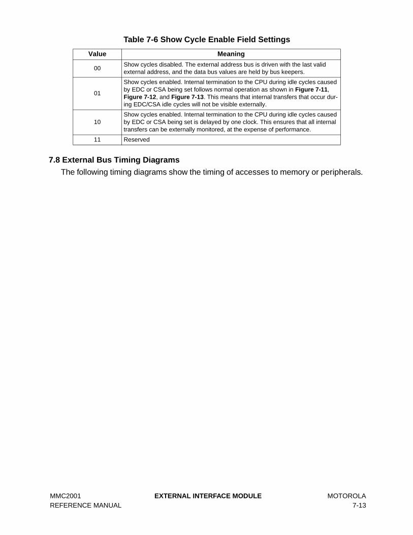
MMC2001 EXTERNAL INTERFACE MODULE MOTOROLA REFERENCE MANUAL 7-13
7.8 External Bus Timing Diagrams
The following timing diagrams show the timing of accesses to memory or peripherals.
Table 7-6 Show Cycle Enable Field Settings
Value Meaning
00Show cycles disabled. The external address bus is driven with the last valid external address, and the data bus values are held by bus keepers.
01
Show cycles enabled. Internal termination to the CPU during idle cycles caused by EDC or CSA being set follows normal operation as shown in Figure 7-11, Figure 7-12, and Figure 7-13. This means that internal transfers that occur dur-ing EDC/CSA idle cycles will not be visible externally.
10Show cycles enabled. Internal termination to the CPU during idle cycles caused by EDC or CSA being set is delayed by one clock. This ensures that all internal transfers can be externally monitored, at the expense of performance.
11 Reserved

MO
TO
RO
LAE
XT
ER
NA
L IN
TE
RFA
CE
MO
DU
LE
MM
C2001
7-14R
EF
ER
EN
CE
MA
NU
AL
Fig
ure 7-6 R
ead M
emo
ry Access (C
SA
= 0, WS
C = 1)
MCU ADDR
MCU R/W
MCU TREQ
CS
OE, EB[0:1]
DATA[15:0]
MCU TA
ADDR[19:0]
MCU DATA
W W S3(S1)S1
XXX
XX
XXXXXXXXX
CLKS2
addr V1 addr V2
addr V1
addr Vx
R
R
R/W
OEA = 1
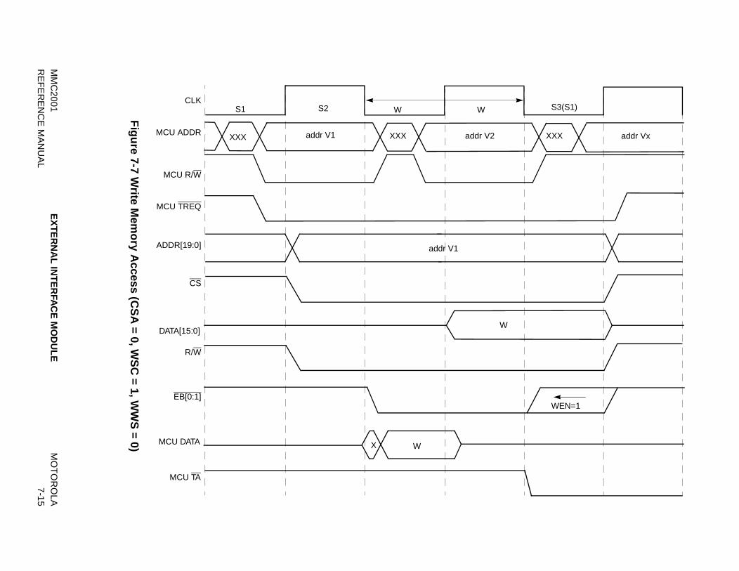
MM
C2001
EX
TE
RN
AL
INT
ER
FAC
E M
OD
UL
EM
OT
OR
OLA
R
EF
ER
EN
CE
MA
NU
AL
7-15
Fig
ure 7-7 W
rite Mem
ory A
ccess (CS
A = 0, W
SC
= 1, WW
S = 0)
MCU ADDR
MCU R/W
MCU TREQ
CS
EB[0:1]
DATA[15:0]
MCU TA
ADDR[19:0]
MCU DATA
S2 W W S3(S1)S1
X
XXX XXX XXX
CLK
addr V1 addr V2 addr Vx
W
addr V1
W
WEN=1
R/W
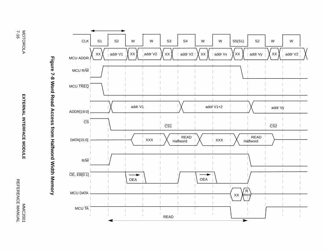
MO
TO
RO
LAE
XT
ER
NA
L IN
TE
RFA
CE
MO
DU
LE
MM
C2001
7-16R
EF
ER
EN
CE
MA
NU
AL
Fig
ure 7-8 W
ord
Read
Access fro
m H
alfwo
rd W
idth
Mem
ory
MCU ADDR
MCU R/W
addr V1
MCU TREQ
addr V1
CS
S1 W W
OE, EB[0:1]
DATA[15:0]
MCU TA
addr V2
addr V1+2
CS1
XX addr V2XX addr VxXX
W W S5(S1)
addr VyXX addr V2XX
S2 W WS2
CS2
ADDR[19:0]
MCU DATA
READ
READXXX
READXXX
WordR
XX
CLK
HalfwordHalfword
S4S3
addr Vy
XX
R/W
OEA OEA
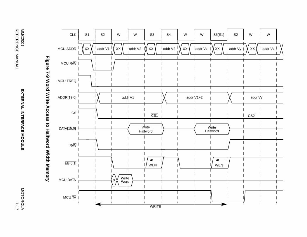
MM
C2001
EX
TE
RN
AL
INT
ER
FAC
E M
OD
UL
EM
OT
OR
OLA
R
EF
ER
EN
CE
MA
NU
AL
7-17
Fig
ure 7-9 W
ord
Write A
ccess to H
alfwo
rd W
idth
Mem
ory
MCU ADDR
MCU R/W
MCU TREQ
CS
S1 W W
EB[0:1]
DATA[15:0]
MCU TA
CS1
W S5(S1) S2 W WS2
CS2
WEN
ADDR[19:0]
MCU DATA
W
WEN
WRITE
addr V1
addr V1 addr V2XX addr V2XX addr VxXX addr VyXX addr VzXXXX
addr Vy
X Write
Write Write
addr V1+2
Word
CLK
Halfword Halfword
S3 S4
R/W

MO
TO
RO
LAE
XT
ER
NA
L IN
TE
RFA
CE
MO
DU
LE
MM
C2001
7-18R
EF
ER
EN
CE
MA
NU
AL
Fig
ure 7-10 W
rite after Read
Mem
ory A
ccess (CS
A = 0, W
SC
= 2, ED
C = 0)
MCU ADDR
MCU R/W
addr V1
MCU TREQ
addr V1
CS
S1 W W
OE,EB[0:1]
DATA[15:0]
MCU TA
addr Vx
addr V2
CS1 CS2
XX addr VyXX
S3(S1) S2
addr V2XX
W S3(S1)
addr VzXX addr VwXX
S2 W
OE, EB EB
ADDR[19:0]
MCU DATA X
W
W
READ WRITE
READ (WSC=2, EDC=0) WRITE (WSC=1, WWS=0)
XX
XX
XX
CLK W W
R
R/W
WENOEA
S2

MM
C2001
EX
TE
RN
AL
INT
ER
FAC
E M
OD
UL
EM
OT
OR
OLA
R
EF
ER
EN
CE
MA
NU
AL
7-19
Fig
ure 7-11 W
rite after Read
Mem
ory A
ccess (CS
A = 0, W
SC
= 1, ED
C = 1)
MCU ADDR
MCU R/W
addr V1
MCU TREQ
addr V1
CS
S1 W W
OE, EB[0:1]
DATA[15:0]
MCU TA
addr Vx
addr Vy
CS1 CS2
XX addr VyXX
S1 S2
addr V2XX
W S3(S1)
addr VzXX addr VwXX
S2 WS2
OE, EB EB
ADDR[19:0]
MCU DATA X
S3
R W
R W
READ (WSC=1, EDC=1) WRITE (WSC=1, WWS=0)
XX
XX
CLK S4 W
IDLE
WEN
R/W
OEA
XX
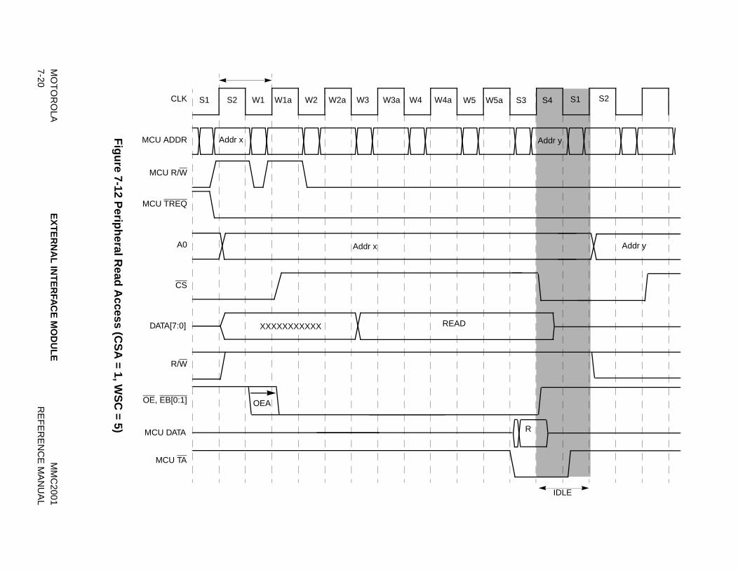
MO
TO
RO
LAE
XT
ER
NA
L IN
TE
RFA
CE
MO
DU
LE
MM
C2001
7-20R
EF
ER
EN
CE
MA
NU
AL
Fig
ure 7-12 P
eriph
eral Read
Access (C
SA
= 1, WS
C = 5)
MCU ADDR
MCU R/W
MCU TREQ
CS
R/W
DATA[7:0]
MCU TA
A0
MCU DATA
S1 S2 W1 W2W1a W2a W3 W3a W4 W4a
Addr x
XXXXXXXXXXX READ
CLK S1W5 S3W5a S4 S2
R
Addr x Addr y
OE, EB[0:1]
Addr y
IDLE
OEA

MM
C2001
EX
TE
RN
AL
INT
ER
FAC
E M
OD
UL
EM
OT
OR
OLA
R
EF
ER
EN
CE
MA
NU
AL
7-21
Fig
ure 7-13 P
eriph
eral Write A
ccess (CS
A = 1, W
SC
= 5)
MCU ADDR
MCU R/W
MCU TREQ
CS
EB[0:1]
DATA[7:0]
MCU TA
ADDR0
MCU DATA
S1 S2 W1 W2W1a W2a W3 W3a W4 W4a
Addr x
CLK S2W5 S3W5a S4 S1
Addr x
W
W
Addr y
Addr y
R/W
WEN
IDLE

MO
TO
RO
LAE
XT
ER
NA
L IN
TE
RFA
CE
MO
DU
LE
MM
C2001
7-22R
EF
ER
EN
CE
MA
NU
AL
Fig
ure 7-14 R
ead an
d W
rite Fast M
emo
ry Access (C
SA
= 0, WS
C = 0, W
WS
= 0)
MCU ADDR
MCU R/W
addr V1
MCU TREQ
addr V1
S1
OE, EB[0:1]
DATA[15:0]
MCU TA
addr V2
CS2 CS2
addr V2XX
S1 S2 S1
addr VyXX
S2S2
OE, EB EB
ADDR[19:0]
MCU DATA XRead Write
READ WRITE
XX
CLK
CS
Read Write
R/W
X
MMC2001 CLOCK MODULE AND LOW-POWER MODES MOTOROLA REFERENCE MANUAL 8-1
SECTION 8CLOCK MODULE AND LOW-POWER MODES
8.1 Overview
The two clock sources to the MMC2001 are a 16.38-MHz clock input pin(HI_REFCLK) and a 32.768-kHz crystal interface. A low-power crystal oscillator cir-cuit (OSC) generates the constant crystal frequency clock LOW_REFCLK from theexternal 32.768 kHz crystal.
The CPU core is clocked by HI_REFCLK.
Peripheral modules can use the following as reference frequencies:
• The 32.768-kHz LOW_REFCLK• The 16.38-MHz HI_REFCLK• A prescaled version of LOW_REFCLK• A combination of several of the above references.
The use of different clocks allows some of the peripherals to maintain a constantoperational frequency even if the 16.38-MHz input signal is shut down. Changing theperipheral frequency or allowing different parts of the same peripheral to use differentfrequencies imply rigid constraints on clock frequencies and synchronization issueswhich must be addressed carefully. Refer to each peripheral definition for furtherdetails.
In addition, the CLKOUT pin can be driven by one of the internal clock sources(LOW_REFCLK or HI_REFCLK) under software control.
The following table describes the clock source for each system block.
Table 8-1 CPU Core and Peripherals Clock SourcePeripheral Peripheral Clock SourceCPU Core HI_REFCLK
External Interface Module HI_REFCLK
UART HI_REFCLKISPI HI_REFCLK
Interrupt Controller HI_REFCLK
PWM HI_REFCLKWatchdog Timer LOW_REFCLK/16384 (2 Hz)
Time-of-Day Timer LOW_REFCLK/128 (256 Hz)
Interval Timer (PIT) LOW_REFCLK/4 (8.192 kHz)1
NOTES:1. When enabled and not low-power disabled
GPIO/KeypadLOW_REFCLK/128 (256 Hz)
for interrupt debouncer JTAG/OnCE HI_REFCLK, TCK

MOTOROLA CLOCK MODULE AND LOW-POWER MODES MMC2001 8-2 REFERENCE MANUAL
The clock module includes the following components:
• Low-power oscillator for generation of LOW_REFCLK• HI_REFCLK receiver and buffer• CLKOUT circuitry• Control circuitry for generation and gating of high frequency clocks to the CPU
and peripherals• Divider circuits for generation of low frequency clocks for peripherals.
A diagram of the clock module is shown in Figure 8-1.

MMC2001 CLOCK MODULE AND LOW-POWER MODES MOTOROLA REFERENCE MANUAL 8-3
Figure 8-1 MMC2001 Clock Module
CPU_CLK
32.768 kHz
16.38 MHz
Peripherals
HI_REFCLK
LOW_REFCLK
EXOSCXOSC
EXTERNAL
VOSC
32.768 kHzR
÷48.192 kHz
R
÷32256 Hz
POR
PIT_RUNNING8.192 kHz * PIT_CLK
TOD_CLK
KPP_CLK
CKO selector
CKOE
CKOSCLKOUT
CLKIN*
!STBY
!STBY &!STOP &!DOZE &!WAIT
R
÷128 2 HzWDOG_CLK
(to CPU, EIM, Interrupt Controller)
!STBY &!STOP
*CLKIN input bufferis a special low signalswing receiver
RBRS**
X1 C1C2
MOTOROLA CLOCK MODULE AND LOW-POWER MODES MMC2001 8-4 REFERENCE MANUAL
8.2 Low-Power Modes
The MMC2001 supports the following features:
• Four low-power modes:— Run — Wait — Doze— Stop
• Ability to shut down all peripherals independently• Ability to shut down the CLKOUT pin.
8.2.1 CPU Core Low-Power Modes
The CPU supports four low-power modes: run, wait, doze, and stop.
8.2.1.1 Run Mode
Run mode is the normal CPU operating mode. Current consumption in this mode isrelated directly to the frequency chosen for the HI_REFCLK (16.38 MHz).
8.2.1.2 Wait Mode
Wait mode is intended to be used to stop only the CPU clock until an interrupt isdetected. In this mode, all peripherals continue operation and can generate inter-rupts, which cause the CPU to exit from wait mode.
8.2.1.3 Doze Mode
Doze mode affects the CPU in the same manner as wait, but with a different code onthe CPU LPMD output signals, which are monitored by peripherals. Each peripheraldefines individual operational characteristics in doze mode. Peripherals which con-tinue to run and have the capability of producing interrupts may cause the CPU to exitthe doze mode and return to the run mode. Peripherals which were stopped willrestart operation on exit from doze mode as defined for each peripheral.
8.2.1.4 Stop Mode
Stop mode affects the CPU in the same manner as wait, but with a different code onthe CPU LPMD output signals, which are monitored by peripherals. In this mode,peripherals cease operation except for the PIT and watchdog timer, which may con-tinue to run (if enabled) using prescaled versions of the LOW_REFCLK clock source.The TOD timer is unaffected in this mode. Several sources exist to exit this mode andreturn to the run mode. See Table 8-2 for more details.
Stopped peripherals stop after entering their individual reset states. When exitingstop mode, most peripherals retain their pre-stop control register values and resumeoperation. Stop mode must be entered in a controlled manner, by shutting down eachperipheral that is going to be stopped after it is ensured that its current operation isproperly terminated.
MMC2001 CLOCK MODULE AND LOW-POWER MODES MOTOROLA REFERENCE MANUAL 8-5
8.2.2 Peripheral Behavior in Low-Power Modes
8.2.2.1 UART
In doze mode, the UART stops activity, if so programmed, after finishing the currentcharacter transmission or reception. Clocks are then shut down until the CPU exitsthe doze mode. When the doze mode is exited, the UART activates its internal clocks,and operation continues from the point reached before entering the doze mode.
In stop mode, the UART stops immediately and freezes its operation, register values,state machines, and external pins. During the stop mode, the UART clocks are shutdown. Coming out of stop mode returns the UART to operation from the mode prior tostop mode entry. To avoid erroneous operation, ensure that the UART is in an idlestate before stop mode is entered.
8.2.2.2 ISPI
In doze mode, the ISPI stops activity, if so programmed, after finishing the currentcharacter transmission or reception. Clocks are then shut down until the CPU exitsthe doze mode. When the doze mode is exited, the ISPI activates its internal clocks,and operation continues from the point reached before entering the doze mode.
In stop mode, the ISPI stops immediately, aborts any transfer in progress, freezes itsoperation and register values, and forgets the state of any transfer in operation. (Thestate machine is reset, and the shift register is cleared.) It is assumed that when stopmode is initiated, there is some other method of shutting down external devices. Dur-ing the stop mode, the ISPI clocks are shut down. Coming out of stop mode returnsthe ISPI to an idle mode. To avoid erroneous operation, ensure that the ISPI is in anidle state before entering the stop mode.
8.2.2.3 PWM
In doze mode, the PWM channel stops activity, if so programmed, after finishing thecurrent period. Clocks are then shut down until the CPU exits the doze mode. Whenthe doze mode is exited, the PWM channel is activated, and operation continues fromthe point reached before doze mode was entered.
In stop mode, the PWM stops immediately and freezes its operation, register values,state machines, and external pins. During the stop mode, the PWM clocks are shutdown. Coming out of stop mode returns the PWM to operation from the state prior tostop mode entry. To avoid erroneous operation, ensure that the PWM is in an idlestate before entering the stop mode.
8.2.2.4 Interrupt Controller
Because the interrupt controller module logic does not depend on the clock forasserting an enabled and requested interrupt to the CPU, none of the low-powermodes have any influence on the module’s functional behavior. The module registerswill not be accessed by the CPU during the low-power mode states. Once a pending
MOTOROLA CLOCK MODULE AND LOW-POWER MODES MMC2001 8-6 REFERENCE MANUAL
interrupt causes an exit from a low power mode (and therefore activation of the CPUclocks as well as the peripheral module clocks), the CPU may access the module reg-isters to determine the interrupt source.
8.2.2.5 Watchdog Timer
The watchdog timer uses a prescaled version of the LOW_REFCLK for its referenceclock. Low-power modes affect this module only if it is considered undesirable for thewatchdog to time out (causing the MMC2001 to reset) when the chip is in stop ordoze mode. In stop and doze mode, if so programmed, the watchdog ceases opera-tion and freezes at the current value. When exiting these modes, the watchdogresumes operation from the freeze value. It is the responsibility of software to avoiderroneous operation.
8.2.2.6 Interval Timer
The interval timer uses a prescaled version of the LOW_REFCLK for its referenceclock. In stop and doze mode, if so programmed, the PIT ceases operation, andfreezes at the current value. When exiting these modes, the PIT resumes operationfrom the freeze value. It is the responsibility of software to avoid erroneous operation.
8.2.2.7 Time-of-Day Timer
The time-of-day timer module uses a prescaled version of the LOW_REFCLK for itsreference clock and does not stop in any of the low power modes.
8.2.2.8 Keypad Port
The keypad port module uses the CPU_CLK for its internal operation only for CPUaccesses, thus the module is not affected by the low power modes and is capable ofwaking up the CPU from all low power modes unless it is explicitly disabled. A pres-caled version of LOW_REFCLK is used for the debounce logic and continues to runin all modes.
8.2.2.9 Peripheral State During Low-Power Modes Summary
The functionality of each of the peripherals and CPU core during the various lowpower modes is summarized in Table 8-2. The status of each peripheral during agiven mode refers to the condition the peripheral automatically assumes when theparticular instruction (wait, doze, or stop) is executed. (It is possible to disable an indi-vidual peripheral by programming its dedicated control bits.) The wake-up capabilityfield refers to the ability of an interrupt from that peripheral to force the CPU into runmode.
8.2.2.10 Standby Mode Summary
The functionality of each of the peripherals and CPU core during the standby mode issummarized in Table 8-2. Standby mode is selected when the LVRSTIN pin isasserted. All modules except for the low-power oscillator (OSC) and the time-of-daytimer (TOD) are held in reset in this mode. The TOD continues to run.

MMC2001 CLOCK MODULE AND LOW-POWER MODES MOTOROLA REFERENCE MANUAL 8-7
Power may or may not be available to peripherals (except for the TOD and OSC) andCPU while in standby mode, depending on the level of VDD. The purpose of this modeis to enable the SRAM and TOD to remain valid while the state of the other on-chipcomponents is undefined.
*Dependent on programming
8.2.3 General Low-Power Features
8.2.3.1 Peripheral Shut Down
Each peripheral may be disabled by software in order to cease internal clock genera-tion and remain in a static state. Each peripheral has its own specific disablingsequence (refer to each peripheral description for further details).
8.2.3.2 CLKOUT Pin Shut Down
This output pin may be disabled in the low state to lower power consumption via theCLKOUT enable (CKOE) bit in the reset/timer block.
Table 8-2 CPU Core and Peripherals in Low-Power Modes
ModulePeripheral Clock Status during Mode/Wake-up Capability
Run Wait Doze Stop Standby
CPU Core Running Stopped Stopped Stopped Stopped
UART Running Running/Yes Prog.*/Yes Stopped/No Stopped/No
ISPI Running Running/Yes Prog.*/Yes Stopped/No Stopped/No
Interrupt Controller Running Stopped/Yes Stopped/Yes Stopped/Yes Stopped/No
EIM Running Stopped/No Stopped/No Stopped/No Stopped/No
PWMs Running Running/Yes Prog.*/Yes Stopped/No Stopped/No
Watchdog Timer Running Running/Yes Prog.*/Yes Prog.*/Yes Stopped/No
Interval Timer (PIT) Running Running/Yes Prog.*/Yes Prog.*/Yes Stopped/No
Time-of-Day Timer (TOD)
Running Running/Yes Running/Yes Running/Yes Running/No
GPIO/Keypad Running Running/Yes Running/Yes Stopped/Yes Stopped/No
OnCE Running Running/Yes Running/Yes Running/Yes Stopped/No

MOTOROLA CLOCK MODULE AND LOW-POWER MODES MMC2001 8-8 REFERENCE MANUAL
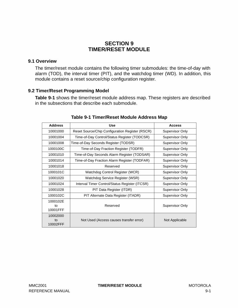
MMC2001 TIMER/RESET MODULE MOTOROLA REFERENCE MANUAL 9-1
SECTION 9TIMER/RESET MODULE
9.1 Overview
The timer/reset module contains the following timer submodules: the time-of-day withalarm (TOD), the interval timer (PIT), and the watchdog timer (WD). In addition, thismodule contains a reset source/chip configuration register.
9.2 Timer/Reset Programming Model
Table 9-1 shows the timer/reset module address map. These registers are describedin the subsections that describe each submodule.
Table 9-1 Timer/Reset Module Address Map
Address Use Access
10001000 Reset Source/Chip Configuration Register (RSCR) Supervisor Only
10001004 Time-of-Day Control/Status Register (TODCSR) Supervisor Only
10001008 Time-of-Day Seconds Register (TODSR) Supervisor Only
1000100C Time-of-Day Fraction Register (TODFR) Supervisor Only
10001010 Time-of-Day Seconds Alarm Register (TODSAR) Supervisor Only
10001014 Time-of-Day Fraction Alarm Register (TODFAR) Supervisor Only
10001018 Reserved Supervisor Only
1000101C Watchdog Control Register (WCR) Supervisor Only
10001020 Watchdog Service Register (WSR) Supervisor Only
10001024 Interval Timer Control/Status Register (ITCSR) Supervisor Only
10001028 PIT Data Register (ITDR) Supervisor Only
1000102C PIT Alternate Data Register (ITADR) Supervisor Only
1000102Eto
10001FFFReserved Supervisor Only
10002000to
10002FFFNot Used (Access causes transfer error) Not Applicable

MOTOROLA TIMER/RESET MODULE MMC2001 9-2 REFERENCE MANUAL
9.3 Reset Operation
9.3.1 Reset Pins
Three reset related pins are provided on MMC2001: a reset input (RSTIN), a low-volt-age detect reset input (LVRSTIN), and a reset output (RSTOUT).
The RSTIN input is an active low input which is connected to external power-on andother reset control sources. This input is qualified as a valid reset if held low for atleast four LOW_REFCLK clock cycles.
The LVRSTIN input is an active low input which is connected to low-voltage detectioncircuitry. No qualification is performed for this input; it must thus be driven in a well-controlled manner.
The RSTOUT output is an active drive pin used to reset external devices. This pin isdriven low when either qualified external resets are detected or on-chip resets(watchdog timer, power-up-reset circuitry) are generated. The minimum length iseight LOW_REFCLK cycles. The RSTOUT pin remains low if either reset input pin isheld low.
9.3.2 Reset Sources
Three sources are capable of generating a reset condition:
• An external qualified low condition on either reset input pin. The RSTIN signalmust be valid low for four LOW_REFCLK clock cycles. LVRSTIN has no qualifi-cation requirements.
• Internal watchdog timer.• Internal power-on reset circuitry.
Figure 9-1 Reset Functional Block Diagram
LOW_REFCLK
4-cycleQual.
WatchdogTimer
4-cyclestretcher
Reset StatusRegister
RSTIN
RSTOUT
To internal resets
4-cyclestretcher
Signal to latch MOD pin
Power-up bypass
LVRSTIN
MOD D QEN
Internal MODsignal to EIM
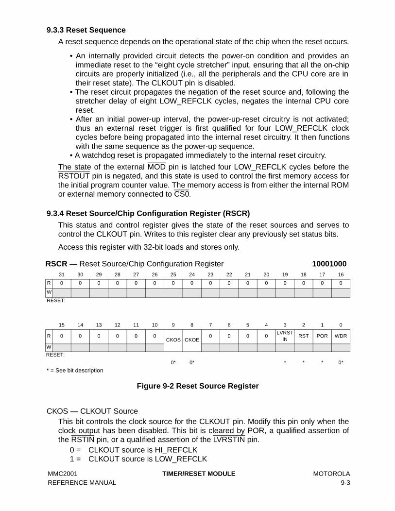
MMC2001 TIMER/RESET MODULE MOTOROLA REFERENCE MANUAL 9-3
9.3.3 Reset Sequence
A reset sequence depends on the operational state of the chip when the reset occurs.
• An internally provided circuit detects the power-on condition and provides animmediate reset to the “eight cycle stretcher” input, ensuring that all the on-chipcircuits are properly initialized (i.e., all the peripherals and the CPU core are intheir reset state). The CLKOUT pin is disabled.
• The reset circuit propagates the negation of the reset source and, following thestretcher delay of eight LOW_REFCLK cycles, negates the internal CPU corereset.
• After an initial power-up interval, the power-up-reset circuitry is not activated;thus an external reset trigger is first qualified for four LOW_REFCLK clockcycles before being propagated into the internal reset circuitry. It then functionswith the same sequence as the power-up sequence.
• A watchdog reset is propagated immediately to the internal reset circuitry.
The state of the external MOD pin is latched four LOW_REFCLK cycles before theRSTOUT pin is negated, and this state is used to control the first memory access forthe initial program counter value. The memory access is from either the internal ROMor external memory connected to CS0.
9.3.4 Reset Source/Chip Configuration Register (RSCR)
This status and control register gives the state of the reset sources and serves tocontrol the CLKOUT pin. Writes to this register clear any previously set status bits.
Access this register with 32-bit loads and stores only.
* = See bit description
Figure 9-2 Reset Source Register
CKOS — CLKOUT SourceThis bit controls the clock source for the CLKOUT pin. Modify this pin only when theclock output has been disabled. This bit is cleared by POR, a qualified assertion ofthe RSTIN pin, or a qualified assertion of the LVRSTIN pin.
0 = CLKOUT source is HI_REFCLK1 = CLKOUT source is LOW_REFCLK
RSCR — Reset Source/Chip Configuration Register 1000100031 30 29 28 27 26 25 24 23 22 21 20 19 18 17 16
R 0 0 0 0 0 0 0 0 0 0 0 0 0 0 0 0
W
RESET:
15 14 13 12 11 10 9 8 7 6 5 4 3 2 1 0
R 0 0 0 0 0 0CKOS CKOE
0 0 0 0LVRST
INRST POR WDR
W
RESET:
0* 0* * * * 0*
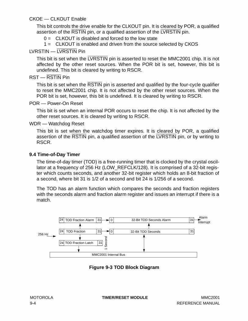
MOTOROLA TIMER/RESET MODULE MMC2001 9-4 REFERENCE MANUAL
CKOE — CLKOUT Enable
This bit controls the drive enable for the CLKOUT pin. It is cleared by POR, a qualifiedassertion of the RSTIN pin, or a qualified assertion of the LVRSTIN pin.
0 = CLKOUT is disabled and forced to the low state1 = CLKOUT is enabled and driven from the source selected by CKOS
LVRSTIN — LVRSTIN Pin
This bit is set when the LVRSTIN pin is asserted to reset the MMC2001 chip. It is notaffected by the other reset sources. When the POR bit is set, however, this bit isundefined. This bit is cleared by writing to RSCR.
RST — RSTIN Pin
This bit is set when the RSTIN pin is asserted and qualified by the four-cycle qualifierto reset the MMC2001 chip. It is not affected by the other reset sources. When thePOR bit is set, however, this bit is undefined. It is cleared by writing to RSCR.
POR — Power-On Reset
This bit is set when an internal POR occurs to reset the chip. It is not affected by theother reset sources. It is cleared by writing to RSCR.
WDR — Watchdog Reset
This bit is set when the watchdog timer expires. It is cleared by POR, a qualifiedassertion of the RSTIN pin, a qualified assertion of the LVRSTIN pin, or by writing toRSCR.
9.4 Time-of-Day Timer
The time-of-day timer (TOD) is a free-running timer that is clocked by the crystal oscil-lator at a frequency of 256 Hz (LOW_REFCLK/128). It is comprised of a 32-bit regis-ter which counts seconds, and another 32-bit register which holds an 8-bit fraction ofa second, where bit 31 is 1/2 of a second and bit 24 is 1/256 of a second.
The TOD has an alarm function which compares the seconds and fraction registerswith the seconds alarm and fraction alarm register and issues an interrupt if there is amatch.
Figure 9-3 TOD Block Diagram
256 Hz
TOD Fraction Latch
MMC2001 Internal Bus
1 S
econ
d
32-Bit TOD Seconds Alarm
32-Bit TOD Seconds
TOD Fraction Alarm
TOD Fraction
Alarm
Interrupt31
0 3124
24 31
31
3124
0

MMC2001 TIMER/RESET MODULE MOTOROLA REFERENCE MANUAL 9-5
9.4.1 TOD Operation
The TOD seconds register (TODSR) is readable and writable at any time. The TODfraction register (TODFR) is always cleared to zero when the TODSR is written.Writes to the TODFR cause the fraction register to be set to all ones, regardless ofthe data written. For read operations, always read the TODSR before the TODFR.This latches the TODFR, which prevents any loss of carry information from the frac-tion to the seconds registers.
The TOD value is matched every 1/256 second to the alarm register if the alarm func-tion is enabled. When a match occurs, the alarm interrupt flag (AIF) is set, and whenthe alarm interrupt enable bit (AIE) is set, an interrupt is issued to the CPU. A write tothe TOD fraction alarm register (TODFAR) clears the AIF. Writes to the TOD secondsalarm register (TODSAR) do not affect the clearing of the AIF.
The alarm match function is temporarily disabled after a write to the TODSAR untilthe TODFAR is written. This prevents an alarm match from occurring before the entire40-bit alarm value is written.
The TOD fraction and seconds counters are undefined after a POR operation and areunaffected by any other reset source. The TOD alarm is disabled by any reset source.
9.4.2 TOD in Low-Power Modes
The TOD is unaffected by the low-power modes. An alarm interrupt may be used toexit from a low power state.
9.4.3 Time-of-Day Control/Status Register (TODCSR)
Figure 9-4 TOD Control/Status Register
Access this register with 32-bit loads and stores only.
AE — Alarm Enable
This bit controls the function of the TOD alarm0 = Alarm function is off to save power1 = Alarm function is on
AIE — Alarm Interrupt Enable
TODCSR — Time-of-Day Control/Status Register 1000100431 30 29 28 27 26 25 24 23 22 21 20 19 18 17 16
R 0 0 0 0 0 0 0 0 0 0 0 0 0 0 0 0
W
RESET:
15 14 13 12 11 10 9 8 7 6 5 4 3 2 1 0
R 0 0 0 0 0 0 0 0 0 0 0 0 0AE AIE AIF
W
RESET:
0 0 0
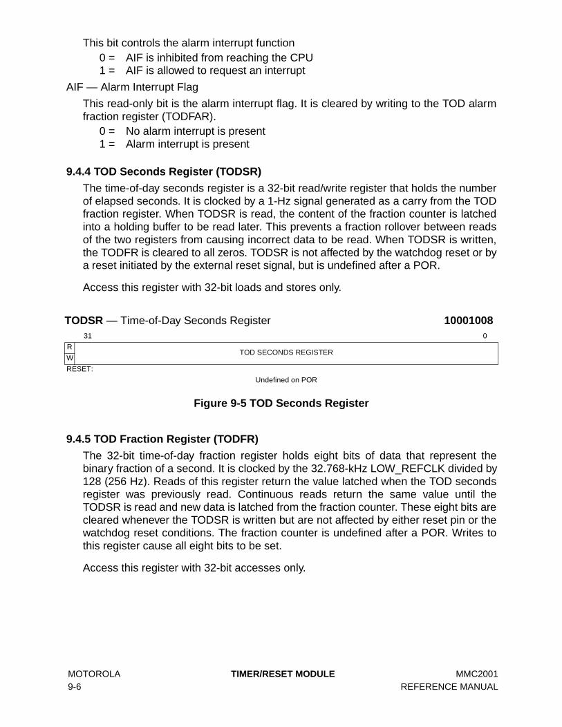
MOTOROLA TIMER/RESET MODULE MMC2001 9-6 REFERENCE MANUAL
This bit controls the alarm interrupt function0 = AIF is inhibited from reaching the CPU1 = AIF is allowed to request an interrupt
AIF — Alarm Interrupt Flag
This read-only bit is the alarm interrupt flag. It is cleared by writing to the TOD alarmfraction register (TODFAR).
0 = No alarm interrupt is present1 = Alarm interrupt is present
9.4.4 TOD Seconds Register (TODSR)
The time-of-day seconds register is a 32-bit read/write register that holds the numberof elapsed seconds. It is clocked by a 1-Hz signal generated as a carry from the TODfraction register. When TODSR is read, the content of the fraction counter is latchedinto a holding buffer to be read later. This prevents a fraction rollover between readsof the two registers from causing incorrect data to be read. When TODSR is written,the TODFR is cleared to all zeros. TODSR is not affected by the watchdog reset or bya reset initiated by the external reset signal, but is undefined after a POR.
Access this register with 32-bit loads and stores only.
Figure 9-5 TOD Seconds Register
9.4.5 TOD Fraction Register (TODFR)
The 32-bit time-of-day fraction register holds eight bits of data that represent thebinary fraction of a second. It is clocked by the 32.768-kHz LOW_REFCLK divided by128 (256 Hz). Reads of this register return the value latched when the TOD secondsregister was previously read. Continuous reads return the same value until theTODSR is read and new data is latched from the fraction counter. These eight bits arecleared whenever the TODSR is written but are not affected by either reset pin or thewatchdog reset conditions. The fraction counter is undefined after a POR. Writes tothis register cause all eight bits to be set.
Access this register with 32-bit accesses only.
TODSR — Time-of-Day Seconds Register 1000100831 0
RTOD SECONDS REGISTER
W
RESET:
Undefined on POR

MMC2001 TIMER/RESET MODULE MOTOROLA REFERENCE MANUAL 9-7
Figure 9-6 TOD Fraction Register
9.4.6 TOD Seconds Alarm Register (TODSAR)
The time-of-day seconds alarm register is a 32-bit read/write register which holdsdata (in seconds) to be compared to the TOD seconds register. The comparison ismade every 1/256 of a second if the alarm function is enabled by the AE bit in theTODCSR. Writes to this register inhibit alarm compares until the TODFAR is written.For proper alarm operation, the fraction alarm register must be (re)written after awrite to this register. This register is not affected by any of the reset conditions.
Access this register with 32-bit loads and stores only.
Figure 9-7 TOD Seconds Alarm Register
9.4.7 TOD Fraction Alarm Register (TODFAR)
The time-of-day fraction alarm register is a 32-bit read/write register which holds eightbits of data to be compared to the TOD fraction register. The comparison is madeevery 1/256 of a second if the alarm function is enabled by the AE bit in the TODCSR.This register is not affected by any of the reset conditions.
Access this register with 32-bit loads and stores only.
TODFR — TOD Fraction Register 1000100C31 30 29 28 27 26 25 24 23 22 21 20 19 18 17 16
R TOD FRACTION REGISTER 0 0 0 0 0 0 0 0
W Set to ones
RESET:
Undefined on POR
15 14 13 12 11 10 9 8 7 6 5 4 3 2 1 0
R 0 0 0 0 0 0 0 0 0 0 0 0 0 0 0 0
W
RESET:
TODSAR — Time-of-Day Seconds Alarm Register 1000101031 0
RTOD SECONDS ALARM REGISTER
W
RESET:
Unaffected
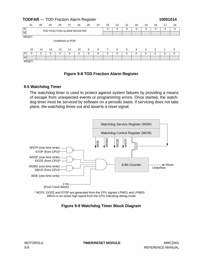
MOTOROLA TIMER/RESET MODULE MMC2001 9-8 REFERENCE MANUAL
Figure 9-8 TOD Fraction Alarm Register
9.5 Watchdog Timer
The watchdog timer is used to protect against system failures by providing a meansof escape from unexpected events or programming errors. Once started, the watch-dog timer must be serviced by software on a periodic basis. If servicing does not takeplace, the watchdog times out and asserts a reset signal.
Figure 9-9 Watchdog Timer Block Diagram
TODFAR — TOD Fraction Alarm Register 1000101431 30 29 28 27 26 25 24 23 22 21 20 19 18 17 16
RTOD FRACTION ALARM REGISTER
0 0 0 0 0 0 0 0
W
RESET:
Undefined on POR
15 14 13 12 11 10 9 8 7 6 5 4 3 2 1 0
R 0 0 0 0 0 0 0 0 0 0 0 0 0 0 0 0
W
RESET:
(From Clock Block)
Reset
WDE (one-time write)
DBUG (from CPU)*WDBG (one-time write)
Watchdog Control Register (WCR)
6-Bit CounterUnderflow
Watchdog Service Register (WSR)W
ST
P
WD
BG
WD
E
STOP (from CPU)*WSTP (one-time write)
DOZE (from CPU)*WDZE (one-time write)
WD
ZE
2 Hz
* NOTE: DOZE and STOP are generated from the CPU signals LPMD1 and LPMD0DBUG is an active high signal from the CPU indicating debug mode

MMC2001 TIMER/RESET MODULE MOTOROLA REFERENCE MANUAL 9-9
9.5.1 Watchdog Timing Specifications
The watchdog timer provides time-out periods from 0.5 seconds up to 32 secondswith a time resolution of 0.5 seconds. It uses a 2-Hz clock derived from aLOW_REFCLK prescaler (divide by 16384) to achieve the resolution of 0.5 seconds.The output of the prescaler circuitry is connected to the input of a 6-bit counter, result-ing in a range of 0.5 to 32 seconds. The time-out period is determined by writing thewatchdog time-out field (WT) in the watchdog control register. Figure 9-9 shows ablock diagram of the watchdog timer.
NOTEThe internal count registers are clocked using the 2-Hz reference. Inorder to read and write these registers accurately via the CPU core(which runs from the CPU_CLK), clock synchronization logic is requiredinternal to the watchdog. This logic requires that the CPU clockfrequency be greater than or equal to the LOW_REFCLK clock fromwhich the counter clocks are derived.
9.5.2 Watchdog Timer after Reset
The watchdog is disabled by default after reset. Once enabled by software, it cannotbe disabled. The watchdog enable bit (WDE) is located in the watchdog control regis-ter. At reset, the watchdog control register and watchdog service register are initial-ized to zero.
9.5.3 Watchdog Timer Service Operation
A service sequence must be executed periodically to keep the watchdog from timingout and causing a reset. The service routine is based on writing to the watchdog ser-vice register. See 9.5.8.2 Watchdog Service Register (WSR).
9.5.4 Watchdog Timer in Wait Mode
In wait mode, all peripheral clocks run normally. The watchdog is not affected.
9.5.5 Watchdog Timer in Doze Mode
In doze mode, the watchdog may either continue to run or be halted. If the WDZE(watchdog doze enable) bit is set in the watchdog control register (WCR), the watch-dog is halted. When doze mode is exited, the watchdog operation reverts to what itwas prior to entering doze mode.
9.5.6 Watchdog Timer in Stop Mode
In stop mode, the watchdog may either continue to run or be halted. If the WSTP(watchdog stop enable) bit is set in the watchdog control register (WCR), the watch-dog is halted. When stop mode is exited, the watchdog operation reverts to what itwas prior to entering stop mode.

MOTOROLA TIMER/RESET MODULE MMC2001 9-10 REFERENCE MANUAL
9.5.7 Watchdog Timer in Debug Mode
In debug mode, the watchdog may either continue to run or be halted. If the WDBG(watchdog debug enable) bit is set in the watchdog control register (WCR), the watch-dog is halted. At this point, the timer is stopped, but register read and write accessesfunction normally. In this mode, the WCR one-time-write lock is disabled and the con-trol bits can be updated.
NOTEIf the WCR is updated in debug mode, it will remain updated whendebug mode is exited.
9.5.8 Watchdog Timer Programming Model
The watchdog programming model consists of a control register and a service regis-ter.
9.5.8.1 Watchdog Control Register (WCR)
This register contains fields that control the operation of the watchdog in differentmodes of operation. The write-once bits can only be written once after a reset condi-tion. Subsequent attempts to write to them will not affect the data previously written.
Access this register with 32-bit loads and stores only.
Figure 9-10 Watchdog Control Register
WT — Watchdog Time-Out
The six-bit WT field contains the time-out value. These bits are reloaded into thewatchdog timer when it has been serviced. After reset, write WT before enabling thewatchdog. The value in WT is loaded into the watchdog counter after running the ser-vice routine as well as on enabling the watchdog timer.
WCR — Watchdog Control Register 1000101C31 30 29 28 27 26 25 24 23 22 21 20 19 18 17 16
R 0 0 0 0 0 0 0 0 0 0 0 0 0 0 0 0
W
RESET:
15 14 13 12 11 10 9 8 7 6 5 4 3 2 1 0
RWT
0 0 0 0 0 0WSTP WDE WDBG WDZE
W
RESET:
0 0 0 0 0 0 0 0 0 0
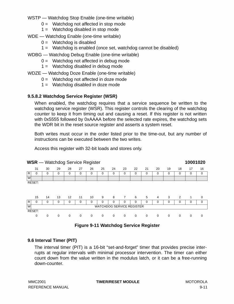
MMC2001 TIMER/RESET MODULE MOTOROLA REFERENCE MANUAL 9-11
WSTP — Watchdog Stop Enable (one-time writable)0 = Watchdog not affected in stop mode1 = Watchdog disabled in stop mode
WDE — Watchdog Enable (one-time writable)0 = Watchdog is disabled1 = Watchdog is enabled (once set, watchdog cannot be disabled)
WDBG — Watchdog Debug Enable (one-time writable)0 = Watchdog not affected in debug mode1 = Watchdog disabled in debug mode
WDZE — Watchdog Doze Enable (one-time writable)0 = Watchdog not affected in doze mode1 = Watchdog disabled in doze mode
9.5.8.2 Watchdog Service Register (WSR)
When enabled, the watchdog requires that a service sequence be written to thewatchdog service register (WSR). This register controls the clearing of the watchdogcounter to keep it from timing out and causing a reset. If this register is not writtenwith 0x5555 followed by 0xAAAA before the selected rate expires, the watchdog setsthe WDR bit in the reset source register and asserts a system reset.
Both writes must occur in the order listed prior to the time-out, but any number ofinstructions can be executed between the two writes.
Access this register with 32-bit loads and stores only.
Figure 9-11 Watchdog Service Register
9.6 Interval Timer (PIT)
The interval timer (PIT) is a 16-bit “set-and-forget” timer that provides precise inter-rupts at regular intervals with minimal processor intervention. The timer can eithercount down from the value written in the modulus latch, or it can be a free-runningdown-counter.
WSR — Watchdog Service Register 1000102031 30 29 28 27 26 25 24 23 22 21 20 19 18 17 16
R 0 0 0 0 0 0 0 0 0 0 0 0 0 0 0 0
W
RESET:
15 14 13 12 11 10 9 8 7 6 5 4 3 2 1 0
R 0 0 0 0 0 0 0 0 0 0 0 0 0 0 0 0
W WATCHDOG SERVICE REGISTER
RESET:
0 0 0 0 0 0 0 0 0 0 0 0 0 0 0 0
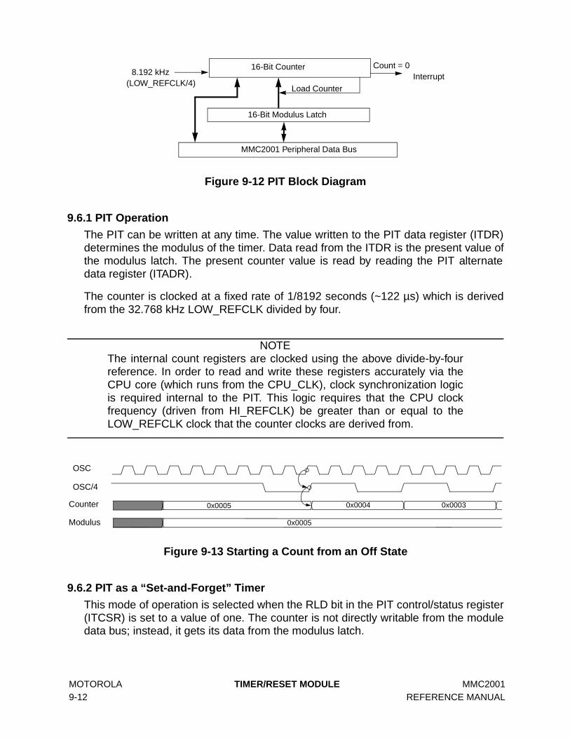
MOTOROLA TIMER/RESET MODULE MMC2001 9-12 REFERENCE MANUAL
Figure 9-12 PIT Block Diagram
9.6.1 PIT Operation
The PIT can be written at any time. The value written to the PIT data register (ITDR)determines the modulus of the timer. Data read from the ITDR is the present value ofthe modulus latch. The present counter value is read by reading the PIT alternatedata register (ITADR).
The counter is clocked at a fixed rate of 1/8192 seconds (~122 µs) which is derivedfrom the 32.768 kHz LOW_REFCLK divided by four.
NOTEThe internal count registers are clocked using the above divide-by-fourreference. In order to read and write these registers accurately via theCPU core (which runs from the CPU_CLK), clock synchronization logicis required internal to the PIT. This logic requires that the CPU clockfrequency (driven from HI_REFCLK) be greater than or equal to theLOW_REFCLK clock that the counter clocks are derived from.
Figure 9-13 Starting a Count from an Off State
9.6.2 PIT as a “Set-and-Forget” Timer
This mode of operation is selected when the RLD bit in the PIT control/status register(ITCSR) is set to a value of one. The counter is not directly writable from the moduledata bus; instead, it gets its data from the modulus latch.
InterruptCount = 0
16-Bit Modulus Latch
MMC2001 Peripheral Data Bus
16-Bit Counter8.192 kHz
Load Counter(LOW_REFCLK/4)
0x0005
OSC
OSC/4
Counter
Modulus
0x0005 0x00030x0004

MMC2001 TIMER/RESET MODULE MOTOROLA REFERENCE MANUAL 9-13
When the counter reaches a count of zero, the PIT interrupt flag (ITIF) is set in theITCSR and the value in the modulus latch is loaded into the counter to be decre-mented towards zero. If the PIT interrupt enable (ITIE) bit is set in the ITCSR, theinterrupt flag issues an interrupt to the CPU.
The counter may by directly initialized, without having to wait for the count to reachzero, when the ITDR is written with the OVW bit in the ITCSR set.
Figure 9-14 Counter Reloading from the Modulus Latch
9.6.3 PIT as a “Free-Running” Timer
This mode of operation is selected when the RLD bit in the ITCSR is cleared to avalue of zero. In this mode, the counter rolls over from 0x0000 to 0xFFFF, withoutreloading from the modulus latch, and continues to count.
When the counter reaches a count of zero, the PIT interrupt flag (ITIF) is set in theITCSR. If the PIT interrupt enable (ITIE) bit is set in the ITCSR, the interrupt flag canissue an interrupt to the CPU.
The counter may by directly initialized, without having to wait for the count to reachzero, when the ITDR is written while the OVW bit is set.
Figure 9-15 Counter in Free-Running Mode
9.6.4 Interval Timer Registers
The interval timer has three registers: the control/status register (ITCSR), the dataregister (ITDR), and the alternate data register (ITADR).
0x0002 0x0001 0x0000 0x0005
0x0005
OSC
OSC/4
COUNTER
MODULUS
ITIF
0x0002 0x0001 0xFFFF
0x0005
OSC
OSC/4
COUNTER
MODULUS
ITIF
0x0000
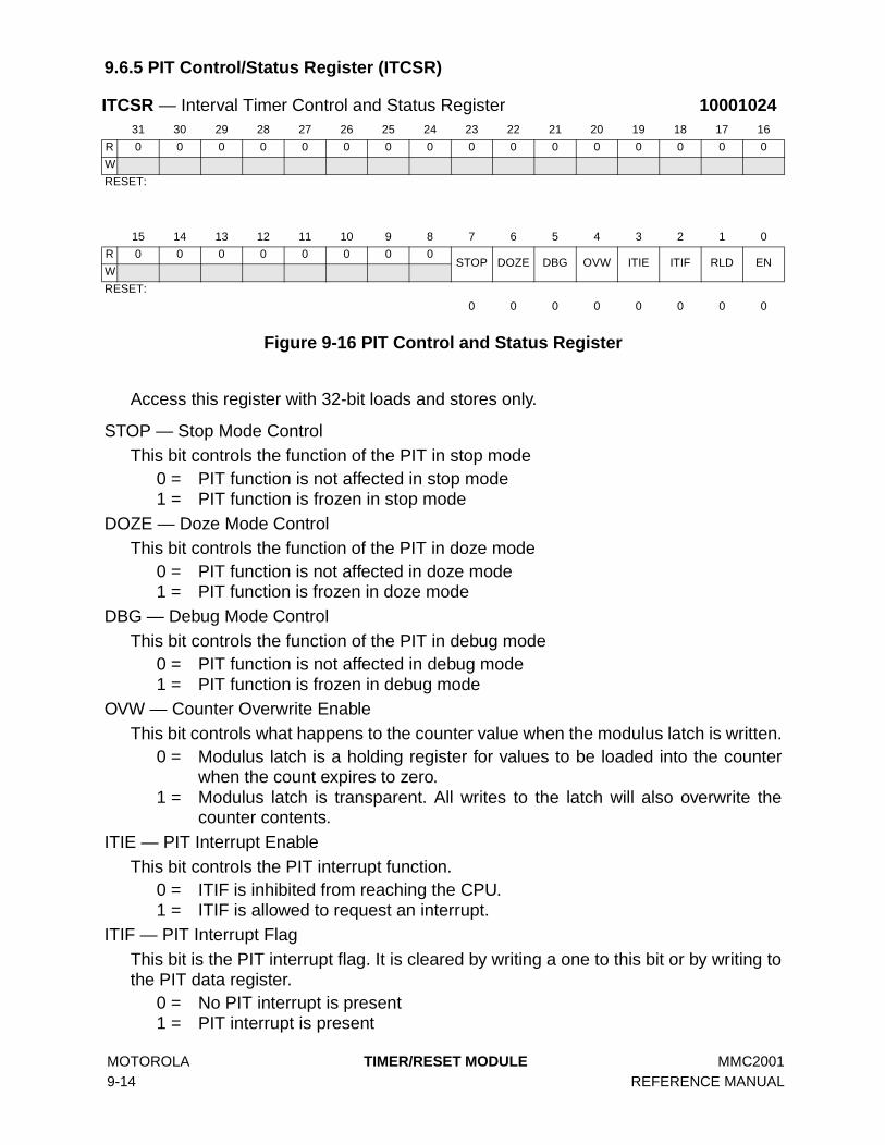
MOTOROLA TIMER/RESET MODULE MMC2001 9-14 REFERENCE MANUAL
9.6.5 PIT Control/Status Register (ITCSR)
Figure 9-16 PIT Control and Status Register
Access this register with 32-bit loads and stores only.
STOP — Stop Mode ControlThis bit controls the function of the PIT in stop mode
0 = PIT function is not affected in stop mode1 = PIT function is frozen in stop mode
DOZE — Doze Mode ControlThis bit controls the function of the PIT in doze mode
0 = PIT function is not affected in doze mode1 = PIT function is frozen in doze mode
DBG — Debug Mode ControlThis bit controls the function of the PIT in debug mode
0 = PIT function is not affected in debug mode1 = PIT function is frozen in debug mode
OVW — Counter Overwrite EnableThis bit controls what happens to the counter value when the modulus latch is written.
0 = Modulus latch is a holding register for values to be loaded into the counterwhen the count expires to zero.
1 = Modulus latch is transparent. All writes to the latch will also overwrite thecounter contents.
ITIE — PIT Interrupt EnableThis bit controls the PIT interrupt function.
0 = ITIF is inhibited from reaching the CPU.1 = ITIF is allowed to request an interrupt.
ITIF — PIT Interrupt FlagThis bit is the PIT interrupt flag. It is cleared by writing a one to this bit or by writing tothe PIT data register.
0 = No PIT interrupt is present1 = PIT interrupt is present
ITCSR — Interval Timer Control and Status Register 1000102431 30 29 28 27 26 25 24 23 22 21 20 19 18 17 16
R 0 0 0 0 0 0 0 0 0 0 0 0 0 0 0 0
W
RESET:
15 14 13 12 11 10 9 8 7 6 5 4 3 2 1 0
R 0 0 0 0 0 0 0 0STOP DOZE DBG OVW ITIE ITIF RLD EN
W
RESET:
0 0 0 0 0 0 0 0

MMC2001 TIMER/RESET MODULE MOTOROLA REFERENCE MANUAL 9-15
RLD — Counter Reload Control
This bit controls whether the value contained in the modulus latch is reloaded into thecounter when the counter reaches a count of zero or whether the counter rolls overfrom zero to 0xFFFF
0 = Counter rolls over to 0xFFFF1 = Counter is reloaded from the modulus latch
EN — PIT Enable
This bit controls the PIT enable function0 = PIT is disabled1 = PIT is enabled
9.6.6 PIT Data Register (ITDR)
On a write, the data becomes the new timer modulus. This value is retained and isused at the next and all subsequent reloads until changed by another write to ITDR.This value is initialized to the maximum count of 0xFFFF on reset. On a read, theITDR returns the value written in the modulus latch. The only way to change the valueof the count directly is to preload a modulus with the OVW bit set to one. The countervalue can be read from the PIT alternate data register.
Access this register with 32-bit loads and stores only.
Figure 9-17 PIT Data Register
ITDR — PIT Data Register 1000102831 30 29 28 27 26 25 24 23 22 21 20 19 18 17 16
R 0 0 0 0 0 0 0 0 0 0 0 0 0 0 0 0
W
RESET:
15 14 13 12 11 10 9 8 7 6 5 4 3 2 1 0
RPIT DATA
W
RESET:
1 1 1 1 1 1 1 1 1 1 1 1 1 1 1 1
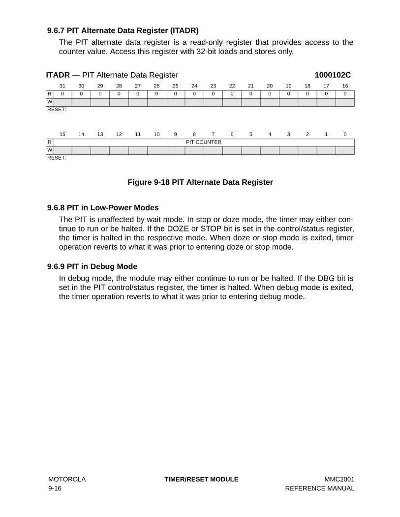
MOTOROLA TIMER/RESET MODULE MMC2001 9-16 REFERENCE MANUAL
9.6.7 PIT Alternate Data Register (ITADR)
The PIT alternate data register is a read-only register that provides access to thecounter value. Access this register with 32-bit loads and stores only.
Figure 9-18 PIT Alternate Data Register
9.6.8 PIT in Low-Power Modes
The PIT is unaffected by wait mode. In stop or doze mode, the timer may either con-tinue to run or be halted. If the DOZE or STOP bit is set in the control/status register,the timer is halted in the respective mode. When doze or stop mode is exited, timeroperation reverts to what it was prior to entering doze or stop mode.
9.6.9 PIT in Debug Mode
In debug mode, the module may either continue to run or be halted. If the DBG bit isset in the PIT control/status register, the timer is halted. When debug mode is exited,the timer operation reverts to what it was prior to entering debug mode.
ITADR — PIT Alternate Data Register 1000102C31 30 29 28 27 26 25 24 23 22 21 20 19 18 17 16
R 0 0 0 0 0 0 0 0 0 0 0 0 0 0 0 0
W
RESET:
15 14 13 12 11 10 9 8 7 6 5 4 3 2 1 0
R PIT COUNTER
W
RESET:

MMC2001 INTERRUPT CONTROLLER MOTOROLA REFERENCE MANUAL 10-1
SECTION 10INTERRUPT CONTROLLER
10.1 Overview
The interrupt controller module collects requests from multiple interrupt sources andprovides an interface to the M•CORE interrupt control lines.
The MMC2001 interrupt controller supports up to 32 interrupt sources (although notall are currently defined). The processor supports two categories of interrupts: normaland fast.
The interrupt controller performs the following functions:
• Indicates pending interrupt sources via a register• Independently enables/disables any interrupt source• Selects normal or fast interrupt request for any interrupt source• Provides a mechanism for software to schedule an interrupt.
The interrupt controller consists of a set of control registers and associated logic toperform interrupt masking and priority support.
The interrupt source register (INTSRC) is a 32-bit control register with a single inter-rupt source associated with each bit. One or more interrupt lines are routed fromeach interrupt source to the INTSRC register. This allows up to 32 distinct interruptsources in an implementation.
A corresponding 32-bit normal interrupt enable register (NIER) allows individual bitmasking of the INTSRC register, and a normal interrupt pending register (NIPND)indicates pending normal interrupt requests. A logical AND is performed on theINTSRC register and the content of the NIER register to form the content of the nor-mal interrupt pending (NIPND) register. A logical bit-wise OR is performed on all theNIPND register bits to form the INT signal routed to the CPU core. This core input sig-nal is maskable by a bit in the PSR.
Two registers support fast interrupt requests. The fast interrupt enable register (FIER)allows individual bit masking of the INTSRC register, and the fast interrupt pendingregister (FIPND) indicates pending fast interrupt requests. A logical AND is performedon the INTSRC register and the content of the FIER register to form the content of thefast interrupt pending (FIPND) register. A logical bit-wise OR is performed on theFIPND register bits to form the FINT signal routed to the CPU core. This core inputsignal is maskable by a bit in the PSR.
These registers are readable by software. In addition, the NIER and FIER registersare writable. Attempted writes to read-only registers are ignored. Access these regis-ters with 32-bit loads and stores only.

MOTOROLA INTERRUPT CONTROLLER MMC2001 10-2 REFERENCE MANUAL
In the MMC2001, interrupt requests to the CPU are always treated as autovectored.The interrupt controller accomplishes this by asserting the CPU AVEC input alongwith the appropriate interrupt request. An interrupt handler can read the NIPND orFIPND register and then vector based on the value received.
The INTSRC register inputs at bit positions [0:2] are reserved for software generationof interrupts and are always forced to a one. By enabling interrupts for these bit posi-tions, software can force an interrupt request.
The interrupt requests are prioritized in the following sequence:
1. Fast interrupt requests
2. Normal interrupt requests
The two interrupt lines INT and FINT are mutually exclusive. If FINT is asserted whileINT is already asserted, INT is automatically negated.
10.2 Interrupt Controller Programming Model
Control and status registers for the interrupt controller begin at address 0x40002000.
10.2.1 Interrupt Source Register (INTSRC)
Access the 32-bit interrupt source register with 32-bit loads only.
Figure 10-1 Interrupt Source Register
Table 10-1 Interrupt Controller Address Map
Address Use Access
10000000 Interrupt Source Register (INTSRC) Supervisor Only
10000004 Normal Interrupt Enable Register (NIER) Supervisor Only
10000008 Fast Interrupt Enable Register (FIER) Supervisor Only
1000000C Normal Interrupt Pending Register (NIPND) Supervisor Only
10000010 Fast Interrupt Pending Register (FIPND) Supervisor Only
INTSRC — Interrupt Source Register 1000000031 30 29 28 27 26 25 24 23 22 21 20 19 18 17 16
IN31 IN30 IN29 IN28 IN27 IN26 IN25 IN24 IN23 IN22 IN21 IN20 IN19 IN18 IN17 IN16
RESET:
15 14 13 12 11 10 9 8 7 6 5 4 3 2 1 0
IN15 IN14 IN13 IN12 IN11 IN10 IN9 IN8 IN7 IN6 IN5 IN4 IN3 1 1 1
RESET:

MMC2001 INTERRUPT CONTROLLER MOTOROLA REFERENCE MANUAL 10-3
INx — Interrupt Source x This bit indicates the state of the corresponding interrupt source.
0 = Negated1 = Asserted
Bits [0:2] of this register are tied to logic level one to allow software to schedule inter-rupts by enabling one or more of these “sources” in the appropriate interrupt enableregister(s) (NIER, FIER).
10.2.2 Normal Interrupt Enable Register (NIER)
Access the 32-bit normal interrupt enable register with 32-bit loads and stores only.
Figure 10-2 Normal Interrupt Enable Register
ENx — Enable Normal Interrupt Flag xThis bit enables the corresponding interrupt source to request a normal interrupt.
0 = Disable 1 = Enable
A reset operation clears this bit. When the enable flag is set and the corresponding interrupt line is asserted, the inter-rupt controller asserts a normal interrupt request. Enabling an interrupt source whichhas an asserted request causes that interrupt to become pending, and a request tothe CPU is asserted if not already outstanding.
10.2.3 Fast Interrupt Enable Register (FIER)Access the 32-bit fast interrupt enable register with 32-bit loads and stores only.
Figure 10-3 Fast Interrupt Enable Register
NIER — Normal Interrupt Enable Register 1000000431 30 29 28 27 26 25 24 23 22 21 20 19 18 17 16
EN31 EN30 EN29 EN28 EN27 EN26 EN25 EN24 EN23 EN22 EN21 EN20 EN19 EN18 EN17 EN16
RESET:
0 0 0 0 0 0 0 0 0 0 0 0 0 0 0 0
15 14 13 12 11 10 9 8 7 6 5 4 3 2 1 0
EN15 EN14 EN13 EN12 EN11 EN10 EN9 EN8 EN7 EN6 EN5 EN4 EN3 EN2 EN1 EN0
RESET:
0 0 0 0 0 0 0 0 0 0 0 0 0 0 0 0
FIER — Fast Interrupt Enable Register 1000000831 30 29 28 27 26 25 24 23 22 21 20 19 18 17 16
EF31 EF30 EF29 EF28 EF27 EF26 EF25 EF24 EF23 EF22 EF21 EF20 EF19 EF18 EF17 EF16
RESET:
0 0 0 0 0 0 0 0 0 0 0 0 0 0 0 0
15 14 13 12 11 10 9 8 7 6 5 4 3 2 1 0
EF15 EF14 EF13 EF12 EF11 EF10 EF9 EF8 EF7 EF6 EF5 EF4 EF3 EF2 EF1 EF0
RESET:
0 0 0 0 0 0 0 0 0 0 0 0 0 0 0 0

MOTOROLA INTERRUPT CONTROLLER MMC2001 10-4 REFERENCE MANUAL
EFx — Enable Fast Interrupt Flag x
This bit enables the corresponding interrupt source to request a fast interrupt. 0 = Disable 1 = Enable
A reset operation clears this bit.
When the enable flag is set and the corresponding interrupt line is asserted, the inter-rupt controller asserts a fast interrupt request. Enabling an interrupt source that hasan asserted request causes that interrupt to become pending, and a request to theCPU is asserted if not already outstanding.
10.2.4 Normal Interrupt Pending Register (NIPND)
Access the 32-bit normal interrupt pending register with 32-bit loads only.
Figure 10-4 Normal Interrupt Pending Register
NPx — Normal Interrupt Pending Flag x
This bit indicates a pending normal interrupt request from the corresponding interruptsource.
0 = No request1 = Interrupt request pending
When a normal interrupt enable flag is set and the corresponding interrupt line isasserted, the interrupt controller asserts a normal interrupt request. The normal inter-rupt pending flags reflect the interrupt input lines which are asserted and are currentlyenabled to generate a normal interrupt.
NIPND — Normal Interrupt Pending Register 1000000C31 30 29 28 27 26 25 24 23 22 21 20 19 18 17 16
NP31 NP30 NP29 NP28 NP27 NP26 NP25 NP24 NP23 NP22 NP21 NP20 NP19 NP18 NP17 NP16
RESET:
0 0 0 0 0 0 0 0 0 0 0 0 0 0 0 0
15 14 13 12 11 10 9 8 7 6 5 4 3 2 1 0
NP15 NP14 NP13 NP12 NP11 NP10 NP9 NP8 NP7 NP6 NP5 NP4 NP3 NP2 NP1 NP0
RESET:
0 0 0 0 0 0 0 0 0 0 0 0 0 0 0 0
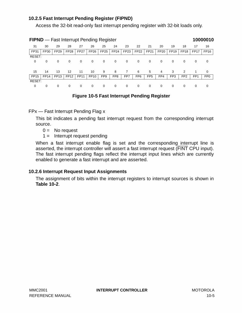
MMC2001 INTERRUPT CONTROLLER MOTOROLA REFERENCE MANUAL 10-5
10.2.5 Fast Interrupt Pending Register (FIPND)
Access the 32-bit read-only fast interrupt pending register with 32-bit loads only.
Figure 10-5 Fast Interrupt Pending Register
FPx — Fast Interrupt Pending Flag x
This bit indicates a pending fast interrupt request from the corresponding interruptsource.
0 = No request1 = Interrupt request pending
When a fast interrupt enable flag is set and the corresponding interrupt line isasserted, the interrupt controller will assert a fast interrupt request (FINT CPU input).The fast interrupt pending flags reflect the interrupt input lines which are currentlyenabled to generate a fast interrupt and are asserted.
10.2.6 Interrupt Request Input Assignments
The assignment of bits within the interrupt registers to interrupt sources is shown inTable 10-2.
FIPND — Fast Interrupt Pending Register 1000001031 30 29 28 27 26 25 24 23 22 21 20 19 18 17 16
FP31 FP30 FP29 FP28 FP27 FP26 FP25 FP24 FP23 FP22 FP21 FP20 FP19 FP18 FP17 FP16
RESET:
0 0 0 0 0 0 0 0 0 0 0 0 0 0 0 0
15 14 13 12 11 10 9 8 7 6 5 4 3 2 1 0
FP15 FP14 FP13 FP12 FP11 FP10 FP9 FP8 FP7 FP6 FP5 FP4 FP3 FP2 FP1 FP0
RESET:
0 0 0 0 0 0 0 0 0 0 0 0 0 0 0 0
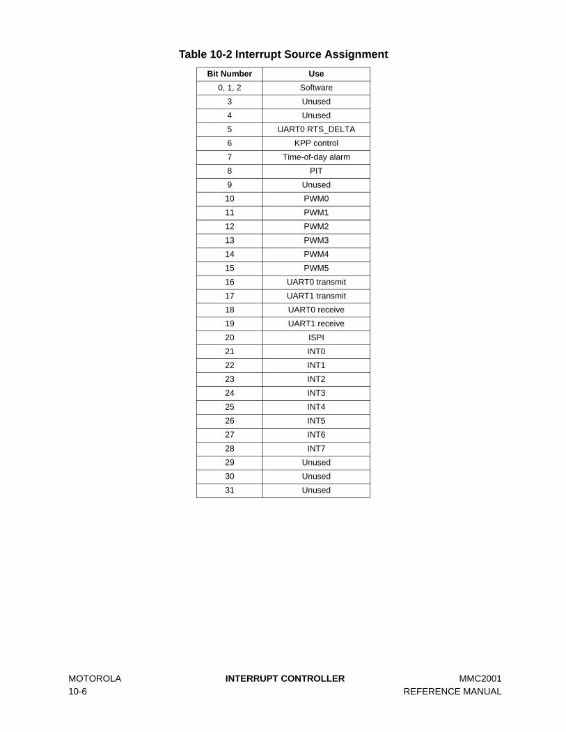
MOTOROLA INTERRUPT CONTROLLER MMC2001 10-6 REFERENCE MANUAL
Table 10-2 Interrupt Source Assignment
Bit Number Use
0, 1, 2 Software
3 Unused
4 Unused
5 UART0 RTS_DELTA
6 KPP control
7 Time-of-day alarm
8 PIT
9 Unused
10 PWM0
11 PWM1
12 PWM2
13 PWM3
14 PWM4
15 PWM5
16 UART0 transmit
17 UART1 transmit
18 UART0 receive
19 UART1 receive
20 ISPI
21 INT0
22 INT1
23 INT2
24 INT3
25 INT4
26 INT5
27 INT6
28 INT7
29 Unused
30 Unused
31 Unused
MMC2001 UNIVERSAL ASYNCHRONOUS RECEIVER/TRANSMITTER MODULE MOTOROLA REFERENCE MANUAL 11-1
SECTION 11UNIVERSAL ASYNCHRONOUS RECEIVER/TRANSMITTER MODULE
11.1 Overview
The universal asynchronous receiver/transmitter (UART) module provides asynchro-nous serial communication with external devices such as modems and other comput-ers. The UART module consists of two independent and almost identical channels.The description of a single channel in this section applies to both UART0 and UART1,with the exception of the CTS and RTS pin functions. These are available only forUART0.
Some of the key features of the UART channels are:
• Full-duplex operation• Direct support of Infrared Data Association mechanism• Robust receiver data sampling with noise filtering• 16-entry FIFOs for transmit and receive• 7- or 8-bit operation with optional even or odd parity and one or two stop bits• Generation and detection of break• 16x bit clock generator for bit rates of 300 bps to 115.2 Kbps • Three maskable interrupts• RTS interrupt with wake up from stop capability• Low-power modes
The UART performs all normal operations associated with “start-stop” asynchronouscommunication. Serial data is transmitted and received at standard bit rates using theinternal 16x bit clock generator.

MOTOROLA UNIVERSAL ASYNCHRONOUS RECEIVER/TRANSMITTER MODULE MMC2001 11-2 REFERENCE MANUAL
Figure 11-1 UART Channel Block Diagram
11.2 UART Signals
11.2.1 RTS — Request to Send (UART0)
An external device requests data from the UART by asserting the RTS input. Whenthe ignore RTS (IRTS) bit is set, the UART ignores the RTS input and sends a charac-ter whenever a character is ready to transmit.
If RTS goes high during transmission, the UART finishes sending the current charac-ter and then shuts off. FIFO content (characters to be transmitted) is undisturbed.
Any transition on the pin can cause an interrupt request to wake up the MCU from lowpower state. Interrupts are enabled by the RTSD EN bit in UART control register 1.
This pin can also be used as a general-purpose input whose status is read in theRTSS bit in the UART status register.
11.2.2 CTS — Clear to Send (UART0)
The UART signals an external device that it is ready to receive data by asserting theCTS output. If the receiver detects a pending overrun, it negates the CTS output.
This pin can also be used as a general purpose output controlled by the CTS bit inUART control register 2.
Transmitter
Data Path
Receiver
Data Path
RxD
TxD
RTS
CTS
M
odul
e In
terfa
ce G
aske
t Blo
ck
16x Bit ClockGenerator
16.38MHz
TX
FIF
OR
X F
IFO
Per
iphe
ral G
aske
t Blo
ck
DataControl
DC
E In
terf
ace
Infr
ared
Inte
rfac
e
HI_REF_CLK

MMC2001 UNIVERSAL ASYNCHRONOUS RECEIVER/TRANSMITTER MODULE MOTOROLA REFERENCE MANUAL 11-3
NOTEThe RTS and CTS signal names follow EIA232 DTE conventions. Thus,RTS is an input and CTS is an output. In many instances, these namesare reversed to reflect device drive direction. Check the specification ofthe remote device to assure correct connection.
11.2.3 TXD — UART Transmit
This pin is the transmitter serial output. In normal mode, NRZ data is output. In infra-red mode, a 3/16 bit-period pulse is output for each zero bit transmitted and no pulsefor each one bit transmitted. For EIA232 standard applications this pin must be con-nected to an EIA232 transmitter to convert voltage levels. TXD can be programmedas a general-purpose I/O pin when the UART TXD function is not being used.
11.2.4 RXD — UART Receive
This pin is the receiver serial input. In normal mode, NRZ data is expected. In infraredmode, a narrow pulse is expected for each zero bit received and no pulse for a one bitreceived. External circuitry must be used to convert the infrared signal to an electricalsignal. EIA232 standard applications require an external EIA232 receiver to convertvoltage levels. RXD can be programmed as a general-purpose I/O pin when theUART RXD function is not being used.
11.3 Sub-Block Description
The UART contains four sub-modules. This section briefly describes the basic func-tionality of the four blocks.
11.3.1 Transmitter
The transmitter accepts a parallel character from the CPU and transmits it serially.The start, stop, and parity (if enabled) bits are added to the character. The transmitterposts a maskable interrupt when it is ready for parallel data. RTS can be used to con-trol the flow of the serial data. If RTS is negated (high), the transmitter finishes send-ing the character in progress (if any) then stops and waits for RTS to again becomeasserted (low).
A break character (continuous zeros) can be generated by the transmitter as well. Fordebugging purposes, parity errors can be generated. The transmitter operates fromthe 1x clock provided by the 16x bit clock generator.
Normal NRZ is transmitted when the infrared interface is disabled.
11.3.2 Receiver
The receiver accepts a serial data stream and converts it into a parallel character.When enabled, it searches for a start bit, qualifies it, and then samples the succeed-ing data bits at the bit-center. Jitter tolerance and noise immunity are provided bysampling at a 16x rate and using voting techniques to clean up the samples. Once the
MOTOROLA UNIVERSAL ASYNCHRONOUS RECEIVER/TRANSMITTER MODULE MMC2001 11-4 REFERENCE MANUAL
start bit has been found, the data bits, parity bit (if parity is enabled), and stop bits areshifted in. If parity is enabled, it is checked and its status is reported in the RX regis-ter. Similarly, frame errors and breaks are checked and reported. When a new char-acter is ready to be read by the host, RX READY is asserted and an interrupt isposted (if enabled). If the receiver register is read as a 16-bit word, the interrupt isautomatically cleared and the data, along with four status bits, are read by the CPU.
CTS can be configured as an output to indicate a pending overrun.
Normal NRZ is expected when the infrared interface is disabled.
11.3.3 Infrared Interface
The infrared interface converts data to be transmitted or received as specified in theIRDA Serial Infrared Physical Layer Specification.
For each zero to be transmitted, a narrow pulse which is 3/16 of a bit time is gener-ated. For each one to be transmitted, no pulse is generated. External circuitry mustbe provided to drive an infrared LED.
When the UART is receiving data, a narrow pulse is expected for each zero transmit-ted, and no pulse is expected for each one transmitted. Circuitry external to the ICtransforms the infrared signal to an electrical signal.
11.3.4 16x Bit Clock Generator
The 16x bit clock generator provides the pre-scaled bit clocks to the transmitter andreceiver blocks. A divide ratio from one to 4096 may be selected in the UBRGR regis-ter. The 16x bit clock generator provides sufficient flexibility to provide almost any“standard” bit-clock from a variety of clock frequencies.
NOTEThe baud rate error is computed as follows for 115.2 Kbps:
The input clock is 16.38 MhzThe divide ratio selected is 9 (UBRGR[11:0] = 8)Actual baud rate: 16.38 Mhz/9/16 = 113.75 khzActual-required rates ratio: 115.2/113.75 = 1.0127
This results in an error-per-bit ratio of 1.27%.
11.3.5 General UART Definitions
The following definitions apply to both the transmitter and receiver operation:
Bit Time — The time required to serially transmit or receive one bit of data.
Start Bit — One bit time of logic zero that indicates the beginning of a data frame. Astart bit must begin with a one-to-zero transition.
Stop Bit — One bit time of logic one that indicates the end of a data frame.

MMC2001 UNIVERSAL ASYNCHRONOUS RECEIVER/TRANSMITTER MODULE MOTOROLA REFERENCE MANUAL 11-5
Frame — A start bit, followed by a specified number of data or information bits, termi-nated by one or two stop bits. The number of data or information bits must agreebetween the transmitting and receiving devices. The most common frame format isone start bit followed by eight data bits (LSB first) terminated by one stop bit, for atotal of ten bit times in the frame. The UART optionally provides other data formats asspecified through the control registers.
Break — A frame in which all the bits are logic zero. This includes the stop bit, whichis normally a logic one, as well as the data bits. This kind of a frame is generally sentto signal the end of a message or the beginning of a new message.
Framing Error — An error condition in which the stop bit of the received frame ismissing. A framing error results when the frame boundaries in the received bit streamare not synchronized with the receiver bit counter. Framing errors are not alwaysdetected: if a data bit in the expected stop bit time happens to be a logic one, theframing error may go undetected. A framing error is always present on the receiverside, when the transmitter is sending breaks. However, if the UART is set up to expecttwo stop bits, and only one is received, then this is not a framing error by definition.
Parity Error — An error condition in which the calculated parity of the received databits in the frame is different from the parity bit received on the RXD line. Parity error isonly calculated after an entire frame is received.
Overrun Error — An error condition in which the latest character received is ignoredto prevent overwriting an already existing character in the UART receiver FIFO. Anoverrun error indicates that the software reading the FIFO is not keeping up with theactual reception of characters on the RXD line.
11.4 UART Programming Model
This section describes the registers in the UART module. Each UART channel hasthe following independent set of registers:
• Three working registers (UCR1, UCR2, USR) that provide all status and controlfunctions for the UART
• A separate test register (UTS) for those applications that need it • Bit-rate generator register (UBRG) that controls the UART bit rate• Separate transmit and receive registers • Port control register that defines the GPIO functionality of UART pins.
The registers are optimized for a 16-bit bus. For example, all status bits associatedwith the received data are available along with the data in a single read. All registerbits are readable (except TX DATA field in the UART transmit register), and most areread/write.
All registers may be accessed either as a halfword or as a byte. The RX and TX dataregisters may also be accessed as 32-bit words. For these registers the upper 16 bitsare forced to zeros.

MOTOROLA UNIVERSAL ASYNCHRONOUS RECEIVER/TRANSMITTER MODULE MMC2001 11-6 REFERENCE MANUAL
Table 11-1 UART Module Address Map
Address Use Access
UART0
10009000 UART0 Receive Register (U0RX) Supervisor Only
10009002 Not Used Supervisor Only
10009004to
1000903EU0RX Echoes On Word Boundaries Supervisor Only
10009040 UART0 Transmit Register (U0TX) Supervisor Only
10009042 Reserved Supervisor Only
10009044to
1000907EU0TX Echoes On Word Boundaries Supervisor Only
10009080 UART0 Control Register 1 (U0CR1) Supervisor Only
10009082 UART0 Control Register 2 (U0CR2) Supervisor Only
10009084 UART0 Baud Rate Generator Register (U0BRGR) Supervisor Only
10009086 UART0 Status Register (U0SR) Supervisor Only
10009088 UART0 Test Register (U0TSR) Supervisor Only
1000908A UART0 Port Control Register (U0PCR) Supervisor Only
1000908C UART0 Data Direction Register (U0DDR) Supervisor Only
1000908E UART0 Port Data Register (U0PDR) Supervisor Only
10009090to
10009FFFReserved Supervisor Only
UART1
1000A000 UART1 Receive Register (U1RX) Supervisor Only
1000A002 Not Used Supervisor Only
1000A004to
1000A03EU1RX Echoes On Word Boundaries Supervisor Only
1000A040 UART1 Transmit Register (U1TX) Supervisor Only
1000A042 Reserved Supervisor Only
1000A044to
1000A07EU1TX Echoes On Word Boundaries Supervisor Only
1000A080 UART1 Control Register 1 (U1CR1) Supervisor Only
1000A082 UART1 Control Register 2 (U1CR2) Supervisor Only
1000A084 UART1 Baud Rate Generator Register (U1BRGR) Supervisor Only
1000A086 UART1 Status Register (U1SR) Supervisor Only
1000A088 UART1 Test Register (U1TSR) Supervisor Only
1000A08A UART1 Port Control Register (U1PCR) Supervisor Only
1000A08C UART1 Data Direction Register (U1DDR) Supervisor Only
1000A08E UART1 Port Data Register (U1PDR) Supervisor Only
1000A088to
1000AFFFReserved Supervisor Only
1000B000to
1FFFFFFFNot Used (Access causes transfer error) Not Applicable

MMC2001 UNIVERSAL ASYNCHRONOUS RECEIVER/TRANSMITTER MODULE MOTOROLA REFERENCE MANUAL 11-7
11.4.1 UART Receive Register (URX)
This read-only register contains received characters and status. After reset, if thereceiver is enabled (RXEN = 1), the CHAR RDY bit is zero until the first character isreceived, and the remainder of the register contents are undefined. The RX register isechoed to 16 word addresses in order to support unloading the FIFO with the loadregister quadrant (ldq) instruction.
*n = 0, 1, . . ., 15X = Undefined
Figure 11-2 UART Receive Register
CHARRDY — Character Ready
This read-only bit indicates whether the character in the RX DATA field and associ-ated flags are valid and ready to be read by the host.
0 = Character in RX DATA field and associated flags are invalid1 = Character in RX DATA field and associated flags valid and ready for reading
At reset, this bit is cleared to zero.
ERR — Error Detect
When set, this read-only bit indicates that the character present in the RX DATA fieldhas an error status. The error can be an OVRRUN, FRMERR, BRK or PRERR. Thisbit is updated and valid for each received character.
0 = No error status detected1 = Error status detected
At reset, this bit is cleared to zero.
OVRRUN — Receiver Overrun
When set, this read-only bit indicates that the receiver ignored data to prevent over-writing the data in the FIFO. Under normal circumstances, this bit should never beset. It indicates that the user’s software is not keeping up with the incoming data rate.This bit is updated and valid for each received character, and when set indicates thatsome number of characters were lost following the character for which the flag is set.
0 = No FIFO overrun1 = A FIFO overrun was detected
At reset, this bit is cleared to zero.
U0RX — UART0 Receive Register 10009000U1RX — UART1 Receive Register 1000A000
15 14 13 12 11 10 9 8 7 6 5 4 3 2 1 0
RCHARRDY
ERROVRRUN
FRMERR
BRKPR
ERR0 0 RX DATA
W
RESET:
0 X X X X X X X X X X X X X X X

MOTOROLA UNIVERSAL ASYNCHRONOUS RECEIVER/TRANSMITTER MODULE MMC2001 11-8 REFERENCE MANUAL
FRMERR — Frame Error
When set, this read-only bit indicates that the current character had a framing error(missing stop bit). The data is possibly corrupted. This bit is updated for each charac-ter read from the FIFO.
Every attempt is made to allow the receiver to correctly interpret data following acharacter marked as having a framing error. (This includes ignoring the start bit vali-dation logic, if appropriate.) However, if the transmitted data includes two stop bits,and both stop bits are incorrect, then the second stop bit will be interpreted as thestart bit of the next character.
0 = Character has no framing error1 = Character has a framing error
At reset, this bit is cleared to zero.
BRK — Break Detect
When set, this read-only bit indicates that the current character was detected as abreak. The data bits are all zero and the stop bit is also zero. The frame error bit isalways set when this bit is set. If odd parity is selected, parity error will also be setwhen this bit is set. This bit is valid for each character read from the FIFO.
0 = Character is not a break character1 = Character is a break character
At reset, this bit is cleared to zero.
PRERR — Parity Error
When set, this read-only bit indicates that the current character was detected with aparity error. The data is possibly corrupted. This bit is updated for each characterread from the FIFO. While parity is disabled, this bit always reads zero.
0 = No parity error detected for data in RX DATA field1 = Parity error detected for data in RX DATA field
At reset, this bit is cleared to zero.
RX DATA — Received Data
These read-only bits are the received character. In 7-bit mode, the MSB is forced tozero. In 8-bit mode, all bits are active.
11.4.2 UART Transmitter Register (UTX)
The UART transmitter register is used by the host to write the data to be transmitted.The low byte is write-only. When this register is read, bits TX[15:8] always return zero,and TX[7:0] is not driving the bus. The TX register is echoed to 16-word addresses inorder to support filling the transmit FIFO with the store register quadrant (stq) instruc-tion.

MMC2001 UNIVERSAL ASYNCHRONOUS RECEIVER/TRANSMITTER MODULE MOTOROLA REFERENCE MANUAL 11-9
*n = 0, 1, . . ., 15X = Undefined
Figure 11-3 UART Transmitter Register
TX DATA — Transmit Data
These write-only bits are the parallel transmit data inputs. In 7-bit mode, D7 isignored. In 8-bit mode, all bits are used. Data is transmitted LSB first. A new charac-ter is transmitted when these bits are written. These bits must be written only whileTRDY is high to ensure that corrupted data is not sent.
11.4.3 UART Control Register 1 (UCR1)
UART control register 1 is a read/write register. This register enables the UART andthe transmit and receive blocks. It controls the Tx and Rx FIFO levels and enables theTRDY and RRDY interrupts.
Figure 11-4 UART Control Register 1
TxFL — Transmitter FIFO Interrupt Trigger Level
These bits control the operation of the interrupt generated by the transmitter. Amaskable interrupt is generated whenever the data level in the TX FIFO drops belowthe selected threshold. The bits are encoded as follows:
At reset, these bits are cleared to zero.
U0TX — UART0 Transmitter Register 10009040U1TX — UART1 Transmitter Register 1000A040
15 14 13 12 11 10 9 8 7 6 5 4 3 2 1 0
0 0 0 0 0 0 0 0
TX DATA
RESET:
0 0 0 0 0 0 0 0 X X X X X X X X
U0CR1 — UART0 Control Register 1 10009080U1CR1 — UART1 Control Register 1 1000A080
15 14 13 12 11 10 9 8 7 6 5 4 3 2 1 0
RTxFL
TRDY-EN
TXEN RxFLRRDY
ENRXEN IREN
0 RTSDEN
SND-BRK
0 0 DOZE
UARTENW
RESET:
0 0 0 0 0 0 0 0 0 0 0 0 0
Table 11-2 TxFL Field Settings
Value Meaning
00 Interrupt if TX FIFO has a slot for one or more character
01 Interrupt if TX FIFO has a slot for four or more characters
10 Interrupt if TX FIFO has a slot for eight or more characters
11 Interrupt if TX FIFO has a slot for fourteen or more characters
MOTOROLA UNIVERSAL ASYNCHRONOUS RECEIVER/TRANSMITTER MODULE MMC2001 11-10 REFERENCE MANUAL
TRDYEN — Transmitter Ready Interrupt EnableSetting this bit enables an interrupt when the transmitter has one or more slots avail-able in the TX FIFO. The fill level in the TX FIFO at which an interrupt is generated iscontrolled by the TxFL bits. While this bit is negated, the transmitter interrupt is dis-abled.
0 = TX interrupt disabled1 = TX interrupt enabled
At reset, this bit is cleared to zero.
TXEN — Transmitter EnableThis bit enables or disables the transmitter. While UARTEN and TXEN bits are set,and DOZE bit is cleared, the transmitter is enabled. If this bit is cleared in the middleof a transmission, the UART disables the transmitter immediately and starts markingones.The transmitter FIFO cannot be written to when this bit is cleared.
0 = Transmitter disabled1 = Transmitter enabled
At reset, this bit is cleared to zero.RxFL — Receiver FIFO Interrupt Trigger Level
These bits control the threshold at which a maskable interrupt will be generated bythe receiver. A maskable interrupt will be generated whenever the data level in the RXFIFO reaches the selected threshold.
At reset, these bits are cleared to zero.RRDYEN — Receiver Ready Interrupt Enable
Setting this bit enables an interrupt when the receiver has data in the RX FIFO. Thefill level in the RX FIFO at which an interrupt is generated is controlled by the RxFLbits. Clearing this bit disables RX interrupts.
0 = RX interrupt disabled1 = RX interrupt enabled
At reset, this bit is cleared to zero.RXEN — Receiver Enable
Setting this bit enables the receiver. When the receiver is enabled, if the RXD line isalready low, the receiver does not recognize break characters, since it requires a validone-to-zero transition before it can accept any character.
0 = Receiver disabled1 = Receiver enabled
At reset, this bit is cleared to zero.
Table 11-3 RxFL Field Settings
Value Meaning
00 Interrupt if RX FIFO contains one or more character
01 Interrupt if RX FIFO contains four or more characters
10 Interrupt if RX FIFO contains eight or more characters
11 Interrupt if RX FIFO contains fourteen or more characters

MMC2001 UNIVERSAL ASYNCHRONOUS RECEIVER/TRANSMITTER MODULE MOTOROLA REFERENCE MANUAL 11-11
IREN — Infrared Interface Enable
Setting this bit enables the infrared interface. Refer to 11.3.3 Infrared Interface.0 = Infrared interface disabled1 = Infrared interface enabled
At reset, this bit is cleared to zero.
RTSD EN — RTS Delta Interrupt Enable
This bit enables or disables RTS delta interrupts. The current status of the RTS pin isread in the UART status register.
0 = RTS interrupt disabled1 = RTS interrupt enabled
At reset, this bit is cleared to zero.
SNDBRK — Send Break
This bit forces the transmitter to send a break character. The transmitter will finishsending the character in progress (if any) and then send break characters until this bitis reset. The user is responsible for ensuring that this bit is high for a sufficient periodof time to generate a valid break; the transmitter samples SNDBRK after every bit istransmitted.
Following completion of the break transmission, the UART transmits two mark bits.The user can continue to fill the FIFO, and any characters remaining will be transmit-ted when the break is terminated. This bit cannot be changed until the UART EN andTX EN bits in the UART control register 1 (CR1) are set.
0 = Do not send break1 = Send break (continuous zeros)
At reset, this bit is cleared to zero.
DOZE — Doze Mode
When the CPU executes a doze instruction and the system is placed in the dozemode, the DOZE bit affects operation of the UART. If this bit is set when the system isin the doze mode, the UART is disabled. Refer to 11.7 UART Operation in Low-Power System Modes.
0 = UART unaffected in doze mode1 = UART disabled in doze mode
At reset, this bit is cleared to zero.
UART EN — UART Enable
This bit enables or disables the UART. If this bit is cleared in the middle of a transmis-sion, the transmitter stops and drives the TXD line to logic one.
0 = UART disabled1 = UART enabled
At reset, this bit is cleared to zero.
11.4.4 UART Control Register 2 (UCR2)
UART control register 2 is a read/write register. This register controls the overall oper-ation of the UART. It controls the clock source, number of bits per character, paritygeneration and checking, and behavior of the RTS, CTS, and DTR pins.

MOTOROLA UNIVERSAL ASYNCHRONOUS RECEIVER/TRANSMITTER MODULE MMC2001 11-12 REFERENCE MANUAL
Figure 11-5 UART Control Register 2
IRTS — Ignore RTS
Setting this bit forces the RTS input signal presented to the transmitter to always beasserted, effectively causing the external pin to be ignored. In this mode, the RTS pincan be used as a general-purpose input.
0 = Transmit only while RTS pin is asserted1 = Ignore RTS pin
At reset, this bit is cleared to zero.
CTSC — CTS Pin Control
This bit controls the operation of the CTS output pin. While this bit is set, the CTS out-put pin is controlled by the receiver. When the RX FIFO has a pending overrun, theCTS output is negated to indicate to the far-end transmitter to stop transmitting. Whilethe CTSC bit is negated, the CTS output pin is controlled by the CTS bit.
On reset, since this bit is cleared to zero, the CTS pin is controlled by the CTS bit,which is also cleared to zero on reset. This means that on reset the CTS signal isnegated.
0 = CTS pin controlled by the CTS bit1 = CTS pin controlled by the receiver
At reset, this bit is cleared to zero.
CTS — CTS bit
This bit controls the CTS pin while the CTSC bit is negated. While CTSC is assertedthis bit has no function.
0 = CTS pin is driven high (inactive)1 = CTS pin is driven low (active)
At reset, this bit is cleared to zero.
PREN — Parity Enable
This bit enables or disables the parity generator in the transmitter and parity checkerin the receiver.
0 = Parity disabled1 = Parity enabled
At reset, this bit is cleared to zero.
U0CR2 — UART0 Control Register 2 10009082U1CR2 — UART1 Control Register 2 1000A082
15 14 13 12 11 10 9 8 7 6 5 4 3 2 1 0
R 0 IRTS CTSC CTS 0 0 0 PREN PROE STPB WS 0 0 0 0 0
W
RESET:
0 0 0 0 0 0 0

MMC2001 UNIVERSAL ASYNCHRONOUS RECEIVER/TRANSMITTER MODULE MOTOROLA REFERENCE MANUAL 11-13
PROE — Parity Odd/Even
This bit controls the sense of the parity generator and checker. When PROE is set,odd parity is generated and expected. When PROE is cleared, even parity is gener-ated and expected. This bit has no function if PREN is low.
0 = Even parity 1 = Odd parity
At reset, this bit is cleared to zero.
STPB — Stop Bits
This bit controls the number of stop bits transmitted after a character. When STPB isset, two stop bits are sent. When STPB is cleared, one stop bit is sent. This bit has noeffect on the receiver, which expects one or more stop bits.
0 = One stop bit transmitted1 = Two stop bits transmitted
At reset, this bit is cleared to zero.
WS — Word Size
This bit specifies a character length of eight or seven bits (not including start, stop, orparity bits). When WS is set, the transmitter and receiver are in eight-bit mode. WhenWS is cleared, they are in seven-bit mode. The transmitter then ignores B7, and thereceiver sets B7 to zero. This bit can be changed between transmissions or recep-tions. If it is changed while a transmission or reception is in progress, however, thelength of the current character being transmitted or received is unpredictable.
0 = 7-bit transmit and receive character length1 = 8-bit transmit and receive character length
At reset, this bit is cleared to zero.
11.4.5 UART BRG Register (UBRGR)
This register specifies the divide ratio of the prescaler in the UART bit clock genera-tor.
Figure 11-6 UART BRG Register
CD — Clock Divider
These bits determine the bit clock generator output rate. The CD field is used to pre-set a 12-bit counter that is decremented at the system clock rate. The value 0x000produces the maximum clock rate (equal to the system clock). The value 0xFFF pro-duces the minimum clock rate (divide by 4096).
U0BRGR — UART0 BRG Register 10009084U1BRGR — UART1 BRG Register 1000A084
15 14 13 12 11 10 9 8 7 6 5 4 3 2 1 0
R 0 0 0 0CD
W
RESET:
0 0 0 0 0 0 0 0 0 0 0 0
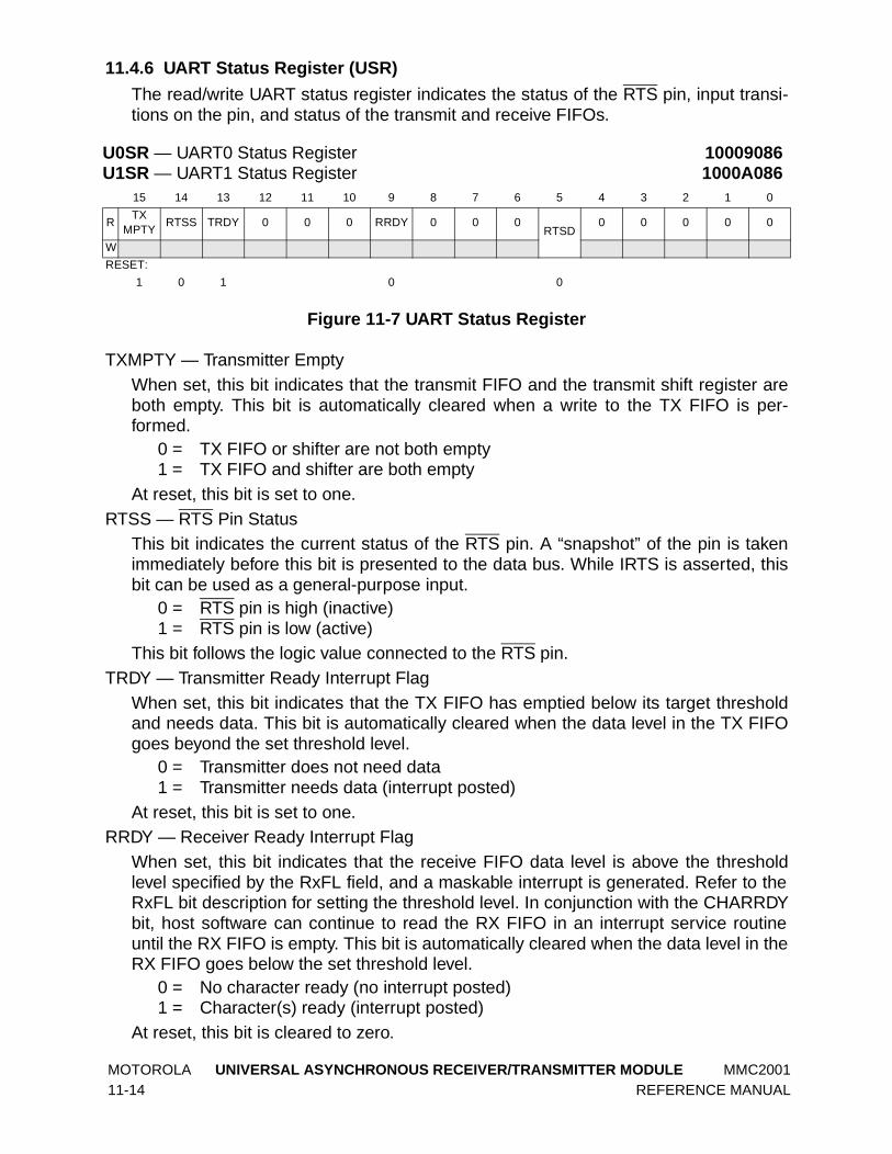
MOTOROLA UNIVERSAL ASYNCHRONOUS RECEIVER/TRANSMITTER MODULE MMC2001 11-14 REFERENCE MANUAL
11.4.6 UART Status Register (USR)
The read/write UART status register indicates the status of the RTS pin, input transi-tions on the pin, and status of the transmit and receive FIFOs.
Figure 11-7 UART Status Register
TXMPTY — Transmitter EmptyWhen set, this bit indicates that the transmit FIFO and the transmit shift register areboth empty. This bit is automatically cleared when a write to the TX FIFO is per-formed.
0 = TX FIFO or shifter are not both empty1 = TX FIFO and shifter are both empty
At reset, this bit is set to one.RTSS — RTS Pin Status
This bit indicates the current status of the RTS pin. A “snapshot” of the pin is takenimmediately before this bit is presented to the data bus. While IRTS is asserted, thisbit can be used as a general-purpose input.
0 = RTS pin is high (inactive)1 = RTS pin is low (active)
This bit follows the logic value connected to the RTS pin.TRDY — Transmitter Ready Interrupt Flag
When set, this bit indicates that the TX FIFO has emptied below its target thresholdand needs data. This bit is automatically cleared when the data level in the TX FIFOgoes beyond the set threshold level.
0 = Transmitter does not need data1 = Transmitter needs data (interrupt posted)
At reset, this bit is set to one.RRDY — Receiver Ready Interrupt Flag
When set, this bit indicates that the receive FIFO data level is above the thresholdlevel specified by the RxFL field, and a maskable interrupt is generated. Refer to theRxFL bit description for setting the threshold level. In conjunction with the CHARRDYbit, host software can continue to read the RX FIFO in an interrupt service routineuntil the RX FIFO is empty. This bit is automatically cleared when the data level in theRX FIFO goes below the set threshold level.
0 = No character ready (no interrupt posted)1 = Character(s) ready (interrupt posted)
At reset, this bit is cleared to zero.
U0SR — UART0 Status Register 10009086U1SR — UART1 Status Register 1000A086
15 14 13 12 11 10 9 8 7 6 5 4 3 2 1 0
RTX
MPTYRTSS TRDY 0 0 0 RRDY 0 0 0
RTSD0 0 0 0 0
W
RESET:
1 0 1 0 0

MMC2001 UNIVERSAL ASYNCHRONOUS RECEIVER/TRANSMITTER MODULE MOTOROLA REFERENCE MANUAL 11-15
RTSD — RTS Delta
When set, this bit indicates that the RTS pin changed state. It generates a maskableinterrupt. In STOP mode, RTS assertion sets this bit to wake the CPU. The currentstate of the RTS pin is available in the RTSS bit. The RTSD interrupt is cleared bywriting a one to this bit.
0 = RTS pin did not change state since last cleared1 = RTS pin changed state
At reset, this bit is cleared to zero.
11.4.7 UART Test Register (UTS)
The UART test register is a read/write register. Unimplemented bits always returnzero when read. This register contains miscellaneous bits to control test features ofthe UART block.
Figure 11-8 UART Test Register
FRC PERR — Force Parity Error
When set, this bit forces the transmitter to generate a parity error if parity is enabled.This bit is provided for system debugging.
0 = Generate normal parity1 = Generate inverted parity (error)
At reset, this bit is cleared to zero.LOOP — Loop TX and RX for Test
This bit controls loopback for test purposes. While this bit is high, the receiver input isinternally connected to the transmitter and ignores the RxD pin. The transmitter isunaffected by this bit. This loopback operates to connect the data on the TxD pindirectly to the voting logic. If infrared mode is enabled (IR_EN is active), the effect ofactivating this bit is to put an IR-formatted bit stream into the voting logic, which willyield odd results. Do not use this loopback if IR_EN is active.
0 = Normal receiver operation1 = Internal connect transmitter output to receiver input
At reset, this bit is cleared to zero.LOOP IR — Loop TX and RX for IR Test
This bit controls a loopback from transmitter to receiver in the infrared interface.0 = No IR loop1 = Connect IR transmit to IR receiver
At reset, this bit is cleared to zero.
U0TS — UART0 Test Register 10009088U1TS — UART1 Test Register 1000A088
15 14 13 12 11 10 9 8 7 6 5 4 3 2 1 0
R 0 0 FRC
PERRLOOP
0 LOOP
IR
0 0 0 0 0 0 0 0 0 0
W
RESET:
0 0 0 0 0 0 0 0 0 0 0 0 0 0 0 0

MOTOROLA UNIVERSAL ASYNCHRONOUS RECEIVER/TRANSMITTER MODULE MMC2001 11-16 REFERENCE MANUAL
11.5 GPIO Pins and Registers
The GPIO functionality of UART pins is controlled by three registers: the port controlregister (UPCR), data direction register (UDDR), and port data register (UPDR).
11.5.1 UART Port Control Register (UPCR)
The read/write UART port control register controls the functionality of UART GPIOpins.
Figure 11-9 UART Port Control Register
PCx — Port Control Bit x 0 = Corresponding pin is configured as GPIO pin1 = Corresponding pin is configured as UART pin
At reset, these bits are cleared to zero.
11.5.2 UART Data Direction Register (UDDR)
The read/write UART data direction register controls the direction of UART GPIOpins.
Figure 11-10 UART Data Direction Register
Table 11-4 UART Pins GPIO Assignment
GPIO Bit UART Pin
P0 RXD
P1 TXD
P2 RTS
P3 CTS
U0PCR — UART0 Port Control Register 1000908AU1PCR — UART1 Port Control Register 1000A08A
15 14 13 12 11 10 9 8 7 6 5 4 3 2 1 0
R 0 0 0 0 0 0 0 0 0 0 0 0PC3 PC2 PC1 PC0
W
RESET:
0 0 0 0
U0DDR — UART0 Data Direction Register 1000908CU1DDR — UART1 Data Direction Register 1000A08C
15 14 13 12 11 10 9 8 7 6 5 4 3 2 1 0
R 0 0 0 0 0 0 0 0 0 0 0 0PDC3 PDC2 PDC1 PDC0
W
RESET:
0 0 0 0
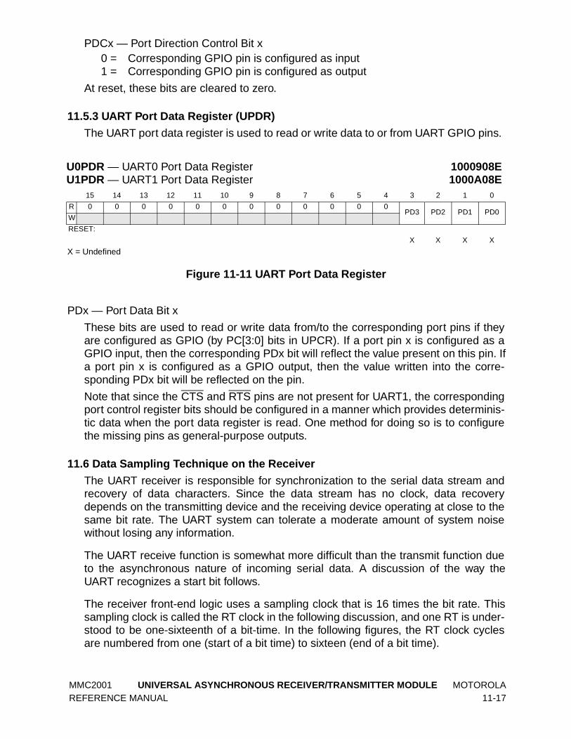
MMC2001 UNIVERSAL ASYNCHRONOUS RECEIVER/TRANSMITTER MODULE MOTOROLA REFERENCE MANUAL 11-17
PDCx — Port Direction Control Bit x 0 = Corresponding GPIO pin is configured as input1 = Corresponding GPIO pin is configured as output
At reset, these bits are cleared to zero.
11.5.3 UART Port Data Register (UPDR)
The UART port data register is used to read or write data to or from UART GPIO pins.
X = Undefined
Figure 11-11 UART Port Data Register
PDx — Port Data Bit x
These bits are used to read or write data from/to the corresponding port pins if theyare configured as GPIO (by PC[3:0] bits in UPCR). If a port pin x is configured as aGPIO input, then the corresponding PDx bit will reflect the value present on this pin. Ifa port pin x is configured as a GPIO output, then the value written into the corre-sponding PDx bit will be reflected on the pin.
Note that since the CTS and RTS pins are not present for UART1, the correspondingport control register bits should be configured in a manner which provides determinis-tic data when the port data register is read. One method for doing so is to configurethe missing pins as general-purpose outputs.
11.6 Data Sampling Technique on the Receiver
The UART receiver is responsible for synchronization to the serial data stream andrecovery of data characters. Since the data stream has no clock, data recoverydepends on the transmitting device and the receiving device operating at close to thesame bit rate. The UART system can tolerate a moderate amount of system noisewithout losing any information.
The UART receive function is somewhat more difficult than the transmit function dueto the asynchronous nature of incoming serial data. A discussion of the way theUART recognizes a start bit follows.
The receiver front-end logic uses a sampling clock that is 16 times the bit rate. Thissampling clock is called the RT clock in the following discussion, and one RT is under-stood to be one-sixteenth of a bit-time. In the following figures, the RT clock cyclesare numbered from one (start of a bit time) to sixteen (end of a bit time).
U0PDR — UART0 Port Data Register 1000908EU1PDR — UART1 Port Data Register 1000A08E
15 14 13 12 11 10 9 8 7 6 5 4 3 2 1 0
R 0 0 0 0 0 0 0 0 0 0 0 0PD3 PD2 PD1 PD0
W
RESET:
X X X X
MOTOROLA UNIVERSAL ASYNCHRONOUS RECEIVER/TRANSMITTER MODULE MMC2001 11-18 REFERENCE MANUAL
When the receiver is first enabled and after the reception of a stop bit at the end of aframe, an asynchronous search is initiated to find the leading edge of the next startbit. (In the case of a framing error, because the stop bit has been somehow cor-rupted, the start-bit validation logic may not operate (because there may not be anegative edge to detect). As long as the voting logic is able to detect a start bit, thereceiver will be able to continue receiving characters following a framing error.)
The goal of this asynchronous search is to gain bit-time synchronization between theserial data stream and the internal RT clock. Once synchronization has been estab-lished, the RT clock controls where the UART perceives the bit-time boundaries to be.The first step in locating a start bit is to find a sample where RXD is zero preceded byfour consecutive samples of logic ones. These five samples are called start-bit qualifi-ers. Until the start-bit qualifiers are detected, the RT clock is reset to state RT1 aftereach sample.
Once the qualifiers are found, the beginning of a start bit is tentatively assumed, andsuccessive samples are assigned successive RT state numbers. The next six sam-ples are taken as start-bit verification samples. If even one of these is a logic one, thelow at RT1 is assumed to have been noise, and the asynchronous search is startedagain. When the start-bit qualifiers and the start-bit verification requirements are met,synchronization has been achieved, and the RT count state is used to determine theposition of bit-time boundaries.
During each bit time, including the start and stop bit times, data samples are taken todetermine the logic sense of the bit time. The samples are taken at RT9, RT10, andRT11 or at RT8, RT9, and RT10, depending upon the synchronization of the incomingdata. The logic sense of the bit time is considered to be the majority of the three sam-ples under consideration. At the end of a character reception, data is transferred fromthe shift register to the parallel receiver register, with the corresponding flags updatedin the receiver register and the status register.
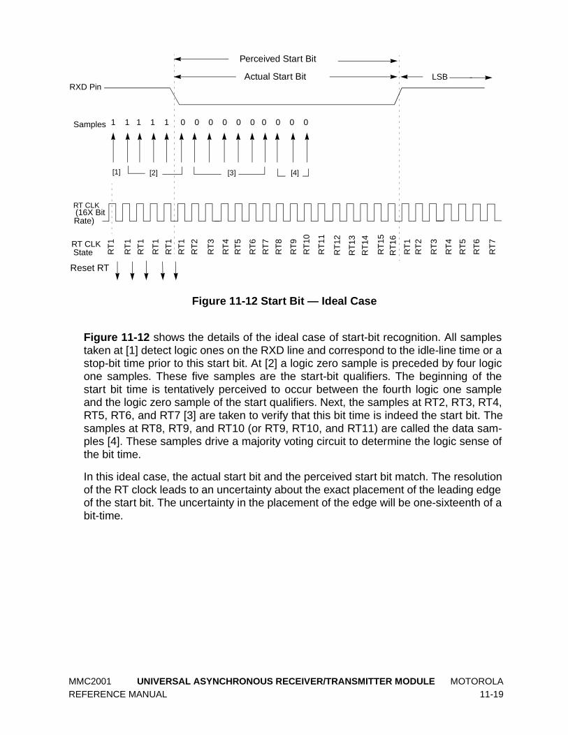
MMC2001 UNIVERSAL ASYNCHRONOUS RECEIVER/TRANSMITTER MODULE MOTOROLA REFERENCE MANUAL 11-19
Figure 11-12 Start Bit — Ideal Case
Figure 11-12 shows the details of the ideal case of start-bit recognition. All samplestaken at [1] detect logic ones on the RXD line and correspond to the idle-line time or astop-bit time prior to this start bit. At [2] a logic zero sample is preceded by four logicone samples. These five samples are the start-bit qualifiers. The beginning of thestart bit time is tentatively perceived to occur between the fourth logic one sampleand the logic zero sample of the start qualifiers. Next, the samples at RT2, RT3, RT4,RT5, RT6, and RT7 [3] are taken to verify that this bit time is indeed the start bit. Thesamples at RT8, RT9, and RT10 (or RT9, RT10, and RT11) are called the data sam-ples [4]. These samples drive a majority voting circuit to determine the logic sense ofthe bit time.
In this ideal case, the actual start bit and the perceived start bit match. The resolutionof the RT clock leads to an uncertainty about the exact placement of the leading edgeof the start bit. The uncertainty in the placement of the edge will be one-sixteenth of abit-time.
RT
1
RT
1
RT
1
RT
1
RT
1
RT
1
RT
2
RT
4R
T5
RT
6
RT
7
RT
8
RT
9
RT
3
RT
10
RT
11
RT
12
RT
13
RT
14
RT
15R
T16
RT
1R
T2
RT
3
RT
4
RT
5
RT
6
RT
7
1 1 1 1 1 0 0 0 0 0 0 0 0 0 0
RXD Pin
Samples
RT CLK(16X Bit
Rate)
RT CLKState
Reset RT
Actual Start Bit
Perceived Start Bit
LSB
[1] [2] [3] [4]

MOTOROLA UNIVERSAL ASYNCHRONOUS RECEIVER/TRANSMITTER MODULE MMC2001 11-20 REFERENCE MANUAL
Figure 11-13 Start Bit — Noise Case One
Figure 11-13 shows what occurs if noise causes a sample to be erroneouslydetected as a zero before the actual beginning of the start bit. The logic zero sample[1] in conjunction with the four preceding samples of logic one meet the conditions forstart qualification; thus, logic tentatively perceives the start bit as beginning here.Subsequent start-verification samples at RT2, RT3, RT4, RT5, RT6, and RT7 [2] arenot all logic zeros; therefore, the tentative placement of the start edge is rejected, andthe search is restarted. When the sample at the actual beginning of the start bit isdetected, the preceding three samples are ones; the start bit is now perceived tobegin here. In this case, the three samples taken at RT2, RT3, RT4, RT5, RT6, andRT7 [3] now verify that the start bit has been found. If the noise bit [1] is further awayfrom the beginning of the actual start bit, the perceived start bit will still be correct.
RT
1
RT
1
RT
1
RT
1
RT
1
RT
2
RT
4
RT
5
RT
6
RT
7
RT
8
RT
9
RT
3
RT
10
RT
11
RT
12
RT
13
RT
14
RT
15
RT
16
RT
1
RT
2
RT
3
1 1 1 0 1 1 1 1 1 1 0 0 0 0 0 0 0
RXD Pin
Samples
RT CLK(16X Bit Rate)
RT CLKState
Reset RT
Actual Start BitPerceived Start Bit
LSB[1]
[2]
RT
4
RT
5
RT
6
RT
7
RT
1
[3]

MMC2001 UNIVERSAL ASYNCHRONOUS RECEIVER/TRANSMITTER MODULE MOTOROLA REFERENCE MANUAL 11-21
Figure 11-14 Start Bit — Noise Case Two
Figure 11-14 is similar to the previous case except noise [1] is now closer to theactual beginning of the start bit. The noise sample and the preceding four logic onesmeet the start qualification requirements. The start verification samples at RT2, RT3,RT4, RT5, RT6, and RT7 [2] are not all zeros; therefore, the tentative placement ofthe start edge is rejected, and the search for the start qualifiers is restarted at [3].Since there are no more cases of four logic ones in a row [3], the start bit is neverdetected. Because the circuit could not locate the start bit, the frame will be receivedas a framing error, improperly received, or missed entirely, depending on the data inthe frame and when the start logic synchronized on what it thought was a start bit.This causes incorrect data reception.
RT
1
RT
1
RT
1
RT
1
RT
1
RT
1
RT
2
RT
3
RT
4
RT
5
RT
1
RT
1
RT
1
RT
1
RT
1
RT
1
RT
1
RT
1
RT
1
RT
1
RT
6
RT
7
RT
1
1 1 1 1 1 1 0 1 1 1 1 0 0 0 0 0 0 0 0 0 0 0 0 0 0 0 0
RXD PIN
Samples
RT CLK(16X Bit Rate)
RT CLKState
Reset RT
Actual Start BitNo start bit found
LSB[1]
[2]
RT
1
RT
1
RT
1
RT
1
RT
1
[3]
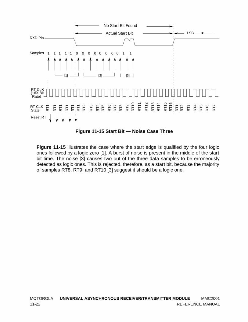
MOTOROLA UNIVERSAL ASYNCHRONOUS RECEIVER/TRANSMITTER MODULE MMC2001 11-22 REFERENCE MANUAL
Figure 11-15 Start Bit — Noise Case Three
Figure 11-15 illustrates the case where the start edge is qualified by the four logicones followed by a logic zero [1]. A burst of noise is present in the middle of the startbit time. The noise [3] causes two out of the three data samples to be erroneouslydetected as logic ones. This is rejected, therefore, as a start bit, because the majorityof samples RT8, RT9, and RT10 [3] suggest it should be a logic one.
RT
1
RT
1
RT
1
RT
1
RT
1
RT
1
RT
2
RT
4R
T5
RT
6
RT
7
RT
8
RT
9
RT
3
RT
10
RT
11
RT
12
RT
13
RT
14
RT
15R
T16
RT
1R
T2
RT
3
RT
4
RT
5
RT
6
RT
7
1 1 1 1 1 0 0 0 0 0 0 0 0 1 1
RXD Pin
Samples
RT CLK(16X Bit
Rate)
RT CLKState
Reset RT
Actual Start Bit
No Start Bit Found
LSB
[1] [2] [3]

MMC2001 UNIVERSAL ASYNCHRONOUS RECEIVER/TRANSMITTER MODULE MOTOROLA REFERENCE MANUAL 11-23
Figure 11-16 Start Bit — Noise Case Four
The case depicted in Figure 11-16 is similar to the previous case. In this case thestart bit is not detected. The frame will be lost or in error, depending on the data in theactual frame and when the start logic got synchronized. In this case, [1] qualifies thestart edge. However, the samples in [2] are not all logic zero due to the presence ofnoise which causes the sample RT7 to be erroneously read as logic one. Thus, thetentative start edge is rejected and the search for the start edge qualifier is startedonce again. This happens even though all the data samples in the start bit [3] werelogic zero. If this were anything but a start bit, the voting logic would have taken theright decision.
11.7 UART Operation in Low-Power System Modes
The UART serial interface operates as long as the 16x bit clock generator is providedwith the system clock. The peripheral interface is operational while the CPU_CLK isrunning. The three bits RXEN, TXEN and UART EN, set by the user, give the capabil-ity to control low-power modes through software. Table 11-5 shows UART functional-ity while in hardware controlled low-power modes.
Table 11-5 UART Low-Power Mode Operation
Normal Mode Wait ModeDoze Mode
Stop ModeDOZE = 0 DOZE = 1
System Clock On On On Off Off
UART Serial Interface On On On Off Off
Module Interface On On On Off Off
RT
1
RT
1
RT
1
RT
1
RT
1
RT
1
RT
2
RT
4R
T5
RT
6
RT
7
RT
1
RT
1
RT
3
RT
1
RT
1
RT
1
RT
1
RT
1
RT
1R
T1
1 1 1 1 1 0 0 0 0 0 0 1 0 0 0 0 0 0 0 0 0
RXD Pin
Samples
RT CLK(16X Bit Rate)
RT CLKState
Reset RT
Actual Start Bit
No Start Bit Found
LSB
[1] [2] [3]

MOTOROLA UNIVERSAL ASYNCHRONOUS RECEIVER/TRANSMITTER MODULE MMC2001 11-24 REFERENCE MANUAL
In doze mode, the UART behavior depends on the DOZE control bit. While the DOZEbit is cleared, the UART serial interface is unaffected. While the system is in dozemode, and the DOZE bit is set, the UART is disabled. If the doze mode is entered withthe DOZE bit set while the UART serial interface was receiving or transmitting data, itwill finish receiving or transmitting the current character and signal to the far-endtransmitter or receiver to stop sending or receiving. There is no guarantee that thedata currently present in the receiver and transmitter FIFOs will not be corrupted.
11.8 UART Operation in System Debug Mode
In debug mode, reads of the UART receiver register do not cause the RX FIFO to“bump.” That is, the value at the read side of the RX FIFO does not change as a resultof reading this register in debug mode. Repeated reads of the UART receiver register,therefore, do not cause its value to change once it contains a valid character.

MMC2001 INTERVAL MODE SERIAL PERIPHERAL INTERFACE MOTOROLA REFERENCE MANUAL 12-1
SECTION 12INTERVAL MODE SERIAL PERIPHERAL INTERFACE
The interval mode serial peripheral interface (ISPI) module provides a high-speedsynchronous serial interface to communicate to external devices such as A/D con-verters and non-volatile RAMs. The ISPI provides the control and clock for data trans-fers and can be configured as either a master or a slave device. In addition, the ISPIincludes a timer that delays the initiation of a serial transfer for a programmableperiod.
12.1 Overview
The ISPI transfers data between the MMC2001 and a peripheral device over a seriallink. Enable and clock signals are used to exchange data between the two devices. Ifthe external device is a transmit-only device (e.g., an A/D converter), the ISPI outputport can be ignored or used for other purposes. Figure 12-1 shows a block diagramof the ISPI.
Figure 12-1 ISPI Channel Block Diagram
12.2 Operation
The ISPI provides three operating modes. Manual mode is a traditional SPI masteroperation mode. Interval mode is similar to manual mode, except that it includes aprogrammable timer to support timed transfers. Interval mode is suitable for control-ling an external sound DAC, for example.
SPI_CLK
SPI_MISO
SPI_MOSI
Module
SPI_EN
SPI_GP
SPI_IRQ
ISPI Interval Bit Baud
State
Control Tx Rx
Shift
Interface
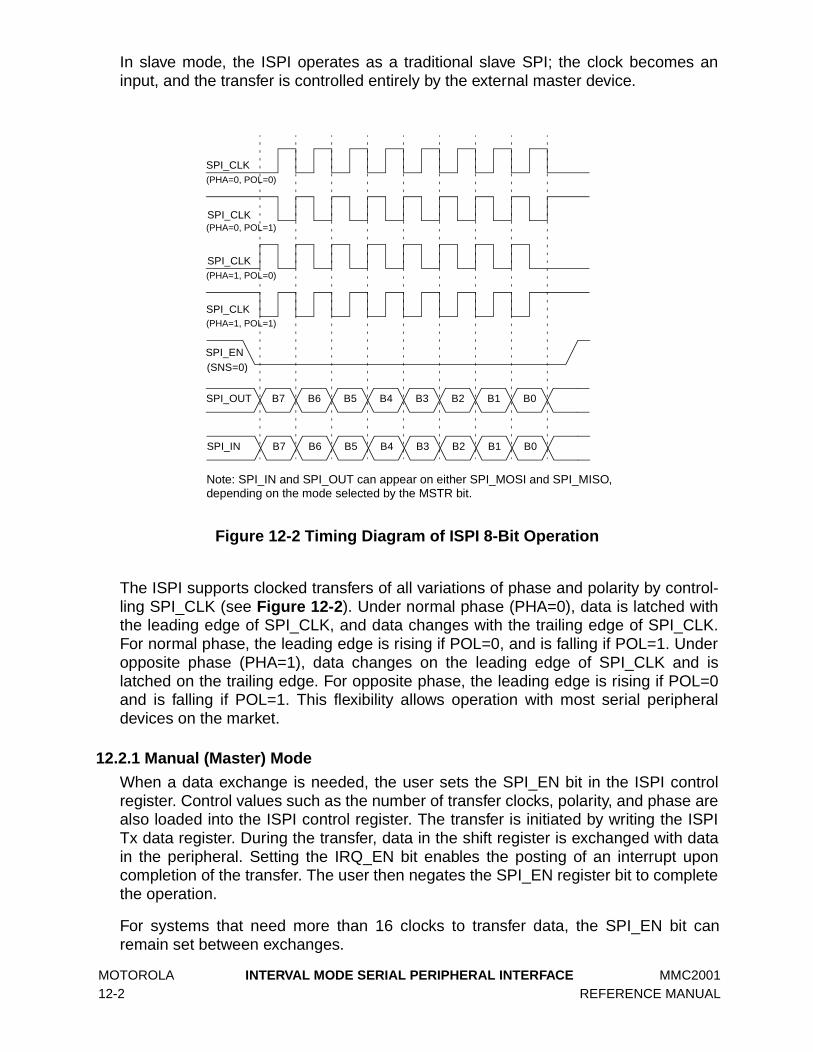
MOTOROLA INTERVAL MODE SERIAL PERIPHERAL INTERFACE MMC2001 12-2 REFERENCE MANUAL
In slave mode, the ISPI operates as a traditional slave SPI; the clock becomes aninput, and the transfer is controlled entirely by the external master device.
Figure 12-2 Timing Diagram of ISPI 8-Bit Operation
The ISPI supports clocked transfers of all variations of phase and polarity by control-ling SPI_CLK (see Figure 12-2). Under normal phase (PHA=0), data is latched withthe leading edge of SPI_CLK, and data changes with the trailing edge of SPI_CLK.For normal phase, the leading edge is rising if POL=0, and is falling if POL=1. Underopposite phase (PHA=1), data changes on the leading edge of SPI_CLK and islatched on the trailing edge. For opposite phase, the leading edge is rising if POL=0and is falling if POL=1. This flexibility allows operation with most serial peripheraldevices on the market.
12.2.1 Manual (Master) Mode
When a data exchange is needed, the user sets the SPI_EN bit in the ISPI controlregister. Control values such as the number of transfer clocks, polarity, and phase arealso loaded into the ISPI control register. The transfer is initiated by writing the ISPITx data register. During the transfer, data in the shift register is exchanged with datain the peripheral. Setting the IRQ_EN bit enables the posting of an interrupt uponcompletion of the transfer. The user then negates the SPI_EN register bit to completethe operation.
For systems that need more than 16 clocks to transfer data, the SPI_EN bit canremain set between exchanges.
SPI_CLK
SPI_EN
SPI_IN
(PHA=0, POL=0)
B7 B6 B5 B4 B3 B2 B1 B0
SPI_OUT B7 B6 B5 B4 B3 B2 B1 B0
SPI_CLK
SPI_CLK
SPI_CLK(PHA=1, POL=1)
(PHA=0, POL=1)
(PHA=1, POL=0)
(SNS=0)
Note: SPI_IN and SPI_OUT can appear on either SPI_MOSI and SPI_MISO, depending on the mode selected by the MSTR bit.
MMC2001 INTERVAL MODE SERIAL PERIPHERAL INTERFACE MOTOROLA REFERENCE MANUAL 12-3
12.2.2 Interval (Master) Mode
Interval mode provides the user with the ability to exchange data at programmed peri-odic intervals. This rate is controlled by three counters: the bit counter, the baudcounter, and the ISPI interval timer. This mode begins operation as soon as theIVL_EN bit is set in the ISPI control register. (If a transfer is in progress, then opera-tion begins upon completion of the existing transfer.) In interval mode (in contrast tomanual mode), the SPI_EN pin is active only when a transfer is in progress; that is, ininterval mode the state machine controls the enable pin. The SPI_EN enable bit (bit12) must still be set in the ISPI control register.
An interval begins with the loading of the actual ISPI interval timer. Once this decre-menting counter reaches zero, the state machine begins the data transfer. When thetransfer is completed, an interrupt is generated (if enabled by IRQ_EN), and the inter-val is completed. At this point the ISPI automatically begins another interval byreloading the interval timer. The length of an interval is governed by the followingequation:
Time_of_Interval = (HI_REFCLK_Period * 2 * (Interval_Count+2)) + (HI_REFCLK_Period * Baud_Count * (Clock_Count+1))
12.2.3 Slave Mode
In slave mode, data exchanges are controlled by external devices through the pinsSPI_CLK and SPI_EN. If pin SPI_EN is enabled (low), then data is latched into theshift register on every other edge of SPI_CLK; the latching edge is determined by thePOL and PHA bits in the ISPI control register. Data is transferred from the shift regis-ter to the ISPI (Rx) data register when pin SPI_EN becomes inactive, or when the bitcounter times out. In addition, IRQ is set at that time (if permitted by IRQ_EN). If theRX data register is not unloaded prior to a new reload, the OVR (ISPI overrun) bit isset in the ISPI status register, and the data is overwritten, causing prior received datato be lost.
SPI_CLK must not exceed HI_REFCLK/16.
12.3 Signal Descriptions
12.3.1 SPI_MISO (Master In, Slave Out)
In either master mode, this pin is the input to the shift register. A new bit is shifted inon each leading edge of SPI_CLK in normal clock mode or on each trailing edge ofSPI_CLK in inverted clock mode. In slave mode, this pin is the output of the shift reg-ister. A new data bit is presented on each trailing edge of the SPI_CLK in normalclock mode (PHA=0). As a slave mode output, SPI_MISO is three-stated when theSPI_EN input is negated.
MOTOROLA INTERVAL MODE SERIAL PERIPHERAL INTERFACE MMC2001 12-4 REFERENCE MANUAL
12.3.2 SPI_MOSI (Master Out, Slave In)
In slave mode, this pin is the input to the shift register. A new bit is shifted in on eachleading edge of SPI_CLK in normal clock mode or on each trailing edge of SPI_CLKin inverted clock mode. In either master mode, this pin is the output of the shift regis-ter. A new data bit is presented on each falling edge of the SPI_CLK in normal clockmode (PHA=0, POL=0).
12.3.3 SPI_EN
In manual mode, this pin is directly controlled by the SPI_EN bit in the ISPI controlregister (bit 12), and can be used as a general-purpose output as well as for enablingan external device. In interval mode, its control is gated by the state machine. As aninput (in slave mode), SPI_EN is active low. As an output (in master modes), theactive sense is determined by the value of bit SNS in the ISPI control register.
12.3.4 SPI_CLK
This pin is the clock output in manual or interval mode. When the ISPI is enabled, aselectable number of clock pulses are issued.
In slave mode, this pin is an input but controls SPI operation just as it does in the twomaster modes. In slave mode, SPI_CLK must not exceed HI_REFCLK/16.
12.3.5 SPI_GP
This output pin is a general-purpose output which can be used as a control signal to aselected external device. The value driven out is controlled by the SPIGP bit in theISPI control register.
12.4 ISPI Programming Model
These registers control the operation of the ISPI and report its status. The data regis-ter exchanges data with external slave devices. After reset, all bits are cleared.
These registers should be accessed with halfword accesses. Accesses other thanhalfword in size result in undefined activity.
Table 12-1 ISPI Module Address Map
Address Use Access
10008000 ISPI Send/Receive Data Register (SPDR) Supervisor Only
10008002 ISPI Control Register (SPCR) Supervisor Only
10008004 ISPI Interval Control Register (SPICR) Supervisor Only
10008006 ISPI Status Register (SPSR) Supervisor Only
10008008to
10008FFFReserved Supervisor Only

MMC2001 INTERVAL MODE SERIAL PERIPHERAL INTERFACE MOTOROLA REFERENCE MANUAL 12-5
12.4.1 ISPI Data Register
The ISPI data register (SPDR) contains data to be exchanged with external devices.Either writing or reading this register clears any set interrupt.
Figure 12-3 ISPI Data Register
Rx DATA — Receive Data
This read-only register contains the data bits received from the shift register. Thosebits more significant than the size determined in CLOCK COUNT (ISPI control regis-ter) return zeros when read. For example, if CLOCK COUNT = 0x8 (9-bit transfer),then bits 15 to 9 are forced to zeros. The value in this register is updated at the end ofevery transfer.
Tx DATA — Transmit Data
This write-only register contains the data bits to be transmitted to the external device.Data is copied from this register to the shift register at the time that the XCH bit is set.
As data is shifted MSB first, outgoing data is MSB-justified relative to the CLOCKCOUNT field in the ISPI control register. For example, if the exchange length is tenbits (CLOCK COUNT = 0x9), the MSB of the outgoing data is bit nine. The first bitpresented to the external device is bit 9, followed by the remaining nine less signifi-cant bits.
12.4.2 ISPI Control Register
The ISPI control register (SPCR), along with the ISPI interval control register, controlsthe operation of the ISPI. Follow this sequence when changing operating modes:
1. Disable the ISPI (COUNT=0) without affecting other fields.
2. Wait for any transfer to complete (XCH bit clear).
3. Update to the new mode.
4. Re-enable the ISPI (COUNT = newcount).
Figure 12-4 ISPI Control Register
SPDR — ISPI Data Register 1000800015 14 13 12 11 10 9 8 7 6 5 4 3 2 1 0
R Rx DATA
W Tx DATA
RESET:
0 0 0 0 0 0 0 0 0 0 0 0 0 0 0 0+
SPCR — ISPI Control Register 1000800215 14 13 12 11 10 9 8 7 6 5 4 3 2 1 0
RDOZE SPI_EN SNS DRV MSTR IRQ_EN PHA POL SPIGP BAUD RATE CLOCK COUNT
W
RESET:
0 0 0 0 0 0 0 0 0 0 0 0 0 0 0 0

MOTOROLA INTERVAL MODE SERIAL PERIPHERAL INTERFACE MMC2001 12-6 REFERENCE MANUAL
DOZE — Doze Mode
When the CPU executes a doze instruction and the system is placed in the dozemode, the DOZE bit affects operation of the ISPI. When this bit is set, the ISPI is dis-abled in doze mode. Refer to the description in 12.6 ISPI Operation in Low-PowerSystem Modes.
0 = ISPI unaffected in doze mode1 = ISPI disabled in doze mode
At reset, this bit is cleared to zero.
SPI_EN — ISPI Enable
In either master mode, this bit controls the value of the SPI_EN pin. The sense of theSPI_EN pin is determined by the SNS bit. In interval mode, the SPI_EN pin isasserted only when XCH is active. The SPI_EN bit must be programmed to a one forany master mode transfer to occur. In slave mode, the ISPI state machine uses theinput value on the SPI_EN pin, and this register bit is ignored. Further, the SPI_ENregister bit will not reflect the value of the SPI_EN pin in slave mode.
0 = Negated1 = Asserted
SNS — SPI_EN Sense
The SNS bit controls the sense of the SPI_EN pin relative to the SPI_EN register bitin the ISPI control register. This is required because in interval mode, the statemachine must assert and then negate the SPI_EN pin. The SNS bit has an effect onlywhen the SPI_EN pin is an output. If the SPI_EN pin is an input, then it is active low,and the SNS bit has no effect.
0 = SPI_EN pin is active low1 = SPI_EN pin is active high
DRV — Drive Type
This bit controls the configuration of the SPI_CLK, SPI_EN and SPI_MOSI outputbuffers in either master mode of the ISPI (MSTR=1). In slave mode, this bit is ignored.
0 = Outputs are totem-pole in either master mode1 = Outputs are open-drain in either master mode
MSTR — Master Mode
This bit controls the mode of the ISPI. In slave mode, the SPI_CLK and SPI_EN pinsare inputs; in the master modes, they are outputs.
0 = ISPI operates in slave mode1 = ISPI operates in either interval mode or manual mode (see IVL_EN in SICR)
IRQ_EN — Interrupt Request Enable
This bit enables/disables the ISPI interrupt request output signal. This bit is cleared tozero on reset.
0 = Interrupts disabled1 = Interrupts enabled

MMC2001 INTERVAL MODE SERIAL PERIPHERAL INTERFACE MOTOROLA REFERENCE MANUAL 12-7
PHA — Phase
This bit controls the phase shift of the SPI_CLK. (See Figure 12-2)0 = Normal phase1 = Shift advance to opposite phase
POL — Polarity
This bit controls the polarity of the SPI_CLK. (See Figure 12-2)0 = Normal polarity1 = Inverted polarity
SPIGP — SPI_GP Control
This bit controls the data on the SPI_GP pin. 0 = Pin driven low1 = Pin driven high
BAUD RATE
These bits select the baud rate of the ISPI bit clock based on divisions of the systemclock. The master clock for the ISPI is HI_REFCLK.
CLOCK COUNT
These bits select the length of the transfer and control the justification of data. Fromtwo to 16 bits can be transferred. A count of all zeros causes the ISPI to be disabled.
Table 12-2 BAUD RATE Field Settings
Value Divide By
000 8
001 16
010 32
011 64
100 128
101 256
110 512
111 1024
Table 12-3 CLOCK COUNT Field Settings
Value Meaning
0000 Disable ISPI
0001 2-bit transfer
.
...
0111 8-bit transfer
.
...
1111 16-bit transfer
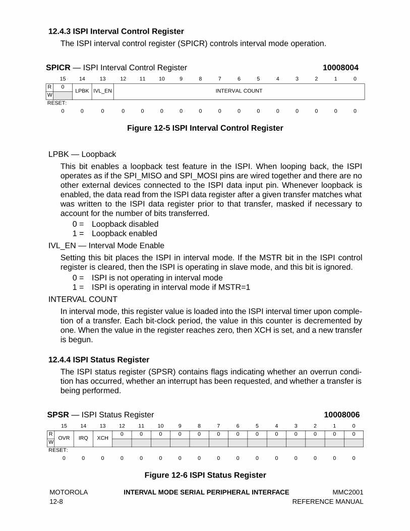
MOTOROLA INTERVAL MODE SERIAL PERIPHERAL INTERFACE MMC2001 12-8 REFERENCE MANUAL
12.4.3 ISPI Interval Control Register
The ISPI interval control register (SPICR) controls interval mode operation.
Figure 12-5 ISPI Interval Control Register
LPBK — Loopback
This bit enables a loopback test feature in the ISPI. When looping back, the ISPIoperates as if the SPI_MISO and SPI_MOSI pins are wired together and there are noother external devices connected to the ISPI data input pin. Whenever loopback isenabled, the data read from the ISPI data register after a given transfer matches whatwas written to the ISPI data register prior to that transfer, masked if necessary toaccount for the number of bits transferred.
0 = Loopback disabled1 = Loopback enabled
IVL_EN — Interval Mode Enable
Setting this bit places the ISPI in interval mode. If the MSTR bit in the ISPI controlregister is cleared, then the ISPI is operating in slave mode, and this bit is ignored.
0 = ISPI is not operating in interval mode1 = ISPI is operating in interval mode if MSTR=1
INTERVAL COUNT
In interval mode, this register value is loaded into the ISPI interval timer upon comple-tion of a transfer. Each bit-clock period, the value in this counter is decremented byone. When the value in the register reaches zero, then XCH is set, and a new transferis begun.
12.4.4 ISPI Status Register
The ISPI status register (SPSR) contains flags indicating whether an overrun condi-tion has occurred, whether an interrupt has been requested, and whether a transfer isbeing performed.
Figure 12-6 ISPI Status Register
SPICR — ISPI Interval Control Register 1000800415 14 13 12 11 10 9 8 7 6 5 4 3 2 1 0
R 0LPBK IVL_EN INTERVAL COUNT
W
RESET:
0 0 0 0 0 0 0 0 0 0 0 0 0 0 0 0
SPSR — ISPI Status Register 1000800615 14 13 12 11 10 9 8 7 6 5 4 3 2 1 0
ROVR IRQ XCH
0 0 0 0 0 0 0 0 0 0 0 0 0
W
RESET:
0 0 0 0 0 0 0 0 0 0 0 0 0 0 0 0
MMC2001 INTERVAL MODE SERIAL PERIPHERAL INTERFACE MOTOROLA REFERENCE MANUAL 12-9
OVR — Overrun
This bit is set by the ISPI controller when a new value is loaded into the RX data reg-ister due to an overrun event. An overrun occurs whenever the RX data register isupdated while holding previously received data that has not been read. This couldoccur when pin SPI_EN becomes inactive and the bit timer has already timed out, orwhen the bit counter times out a second time while SPI_EN remains continuouslyasserted. It could also be set in interval or manual master mode if the RX data regis-ter is not read between transfers. In these cases, the OVR bit may be ignored ifappropriate.
0 = No overrun event has occurred1 = An overrun event has occurred
This bit is cleared by writing it to zero or by reset.
IRQ — Interrupt Request
This register bit is cleared on either a write or a read of the ISPI data register, andwhen set indicates that an interrupt has been requested.
0 = No interrupt has been requested1 = An interrupt has been requested
XCH — Exchange
This bit indicates whether the state machine is performing a transfer. In manualmode, XCH is set by writing the ISPI data register. In interval mode, XCH is set auto-matically by the interval timer. In slave mode, XCH is set when pin SPI_EN isasserted and is negated briefly once the counters determine the completion of atransfer. It is then reasserted if SPI_EN is still asserted. In all modes, XCH is resetupon completion of a transfer.
0 = SPI is idle or interval timer is operating1 = Initiate exchange or exchange in progress
12.5 ISPI Programming Examples
12.5.1 Manual Mode Example
Manual mode is the simplest of the transfer methods.
Assume that the transfer to be performed is bidirectional, and the receive data is 12bits. The data to be sent is 0x0013, and the external device will receive and keep all12 bits. The external device is such that PHA=1, POL=0 is desired, with an active lowenable. An interrupt is required following the transfer to indicate when data is avail-able. The device accepts data at a clock rate between 100 kHz and 1 MHz, and theMMC2001 uses a 16.38-MHz clock.
To program the ISPI to perform such a transfer:
1. Write ISPI register SPCR to 0x4E4B.
2. Write ISPI register SPDR to 0x0013.
MOTOROLA INTERVAL MODE SERIAL PERIPHERAL INTERFACE MMC2001 12-10 REFERENCE MANUAL
The value to be written into the ISPI control register is determined as follows:
• (Assume DOZE = 0)• Assign SNS = 0 to force enable to active low.• Assign SPI_EN = 1 to enable the pin• Assign MSTR = 1• Assign IRQ_EN = 1 to enable interrupts• Assign PHA = 1• Assign POL = 0• Assign BAUD RATE = 4 to divide 16 MHz down to approximately 128 kHz per bit• Assign CLOCK COUNT = 0xB to transfer 12 bits.
12.5.2 Slave Mode Example
In slave mode, the timing of transfers is dependent entirely on the external device. Ifthe transfer parameters for this example are identical to those in the manual modeexample above, then the ISPI is programmed in a two-step process:
1. Write ISPI register SPCR to 0x060B.
2. Write ISPI register SPDR to 0x0013.
SPCR is programmed differently from the manual mode example because:
• SPI_EN, SNS, and BAUD RATE are ignored in slave mode.• MSTR has to be cleared to enable slave mode.
12.5.3 Interval Model Example
With a 16.38-MHz clock, HI_REFCLK = 61 ns. To program the ISPI to transfer 10-bitwords at 8-kHz intervals:
1. Program clock count to 0x9
2. Program baud rate to 0x3 (divide HI_REFCLK by 64)
3. Set SPI_EN, PHA, POL, and SNS as desired
4. Program interval count to 0x29F (671 decimal)
Per the equation:
Time_of_Interval = (HI_REFCLK_Period * 2 * (Interval_Count+2)) + (HI_REFCLK_Period * Baud_Count * (Clock_Count +1))
Time_of_Interval is then set to the following:
61 * 2 * (671 + 2) + (61 * 64 * 11) = 125.05 µs.
The ISPI interval timer begins as soon as written, following the transfer period. Thisleaves approximately 1406 HI_REFCLK cycles before the Tx data register must bere-written.
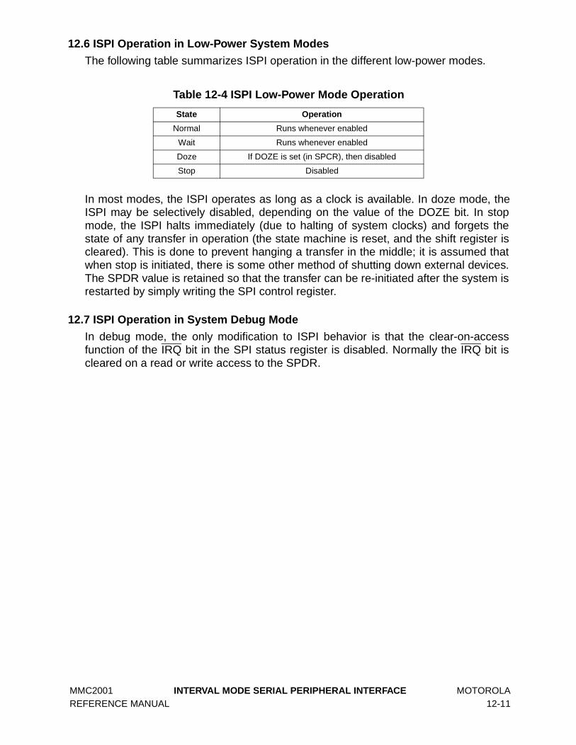
MMC2001 INTERVAL MODE SERIAL PERIPHERAL INTERFACE MOTOROLA REFERENCE MANUAL 12-11
12.6 ISPI Operation in Low-Power System Modes
The following table summarizes ISPI operation in the different low-power modes.
In most modes, the ISPI operates as long as a clock is available. In doze mode, theISPI may be selectively disabled, depending on the value of the DOZE bit. In stopmode, the ISPI halts immediately (due to halting of system clocks) and forgets thestate of any transfer in operation (the state machine is reset, and the shift register iscleared). This is done to prevent hanging a transfer in the middle; it is assumed thatwhen stop is initiated, there is some other method of shutting down external devices.The SPDR value is retained so that the transfer can be re-initiated after the system isrestarted by simply writing the SPI control register.
12.7 ISPI Operation in System Debug Mode
In debug mode, the only modification to ISPI behavior is that the clear-on-accessfunction of the IRQ bit in the SPI status register is disabled. Normally the IRQ bit iscleared on a read or write access to the SPDR.
Table 12-4 ISPI Low-Power Mode Operation
State Operation
Normal Runs whenever enabled
Wait Runs whenever enabled
Doze If DOZE is set (in SPCR), then disabled
Stop Disabled

MOTOROLA INTERVAL MODE SERIAL PERIPHERAL INTERFACE MMC2001 12-12 REFERENCE MANUAL

MMC2001 EXTERNAL INTERRUPTS/GPIO (EDGE PORT) MOTOROLA REFERENCE MANUAL 13-1
SECTION 13EXTERNAL INTERRUPTS/GPIO (EDGE PORT)
13.1 Overview
The MMC2001 has eight external interrupt pins. Each pin can be configured individu-ally as a level-sensitive interrupt, an edge-detecting interrupt (rising edge, fallingedge, or both), or a general-purpose I/O pin.
Figure 13-1 External Interrupt/GPIO Block Diagram
13.2 Interrupt/General-Purpose I/O Pin Descriptions (INT[0:7])
When programmed as inputs, these pins use Schmitt triggered input buffers. Whenedge triggered, triggering occurs at a voltage level and is not directly related to the falltime of the interrupt signal. However, as the fall time of the interrupt signal increases,the probability of generating multiple interrupts due to this “noise” also increases. Alldefault to general-purpose input pins at reset. The interrupt request function on thesepins is masked in the interrupt controller fast interrupt enable register (FIER) and nor-mal interrupt enable register (NIER).
EPPAR[2n]
EPPAR[2n+1]
EPPAR[2n+1]EPPAR[2n]
To InterruptController
EPDDR[n]
EPDR[n]
Data
RisingEdge Detect
FallingEdge Detect
EPFR[n]
Bus
EPPAR[2n, 2n+1]

MOTOROLA EXTERNAL INTERRUPTS/GPIO (EDGE PORT) MMC2001 13-2 REFERENCE MANUAL
13.3 Edge Port Programming Model
The edge port programming model consists of the following registers:
• The edge port pin assignment register (EPPAR) controls the function of each pinindividually.
• The edge port data direction register (EPDDR) controls the direction of each oneof the pins individually.
• The edge port data register (EPDR) holds the data to be driven to the pins.• The edge port flag register (EPFR) latches the edge event for each one of the
pins individually.
Access the edge port registers with halfword accesses.
13.3.1 Edge Port Pin Assignment Register (EPPAR)
The 16-bit read/write edge port pin assignment register (EPPAR) configures each ofthe interrupt pins as either level-sensitive or edge-triggered. Rising, falling, or bothedges can be selected as the active edge. Requests are always generated out of thisblock but may be masked within the interrupt controller module. The functionality ofthis register is independent of the programmed pin direction.
Figure 13-2 Edge Port Pin Assignment Register
EPPAx — Edge Port Pin Assignment Select Field x
Pins configured as level-sensitive are inverted so that a logic low on the external pinrepresents a valid interrupt request. Level-sensitive interrupt inputs are not latched.To guarantee that a level-sensitive interrupt request is acknowledged, the interruptsource must keep the signal asserted until acknowledged by software.
Pins configured as edge-sensitive interrupts are latched and need not remainasserted for interrupt generation. When the pin is programmed to use the edgedetecting circuit, its state is monitored regardless of its configuration as input or out-put.
Table 13-1 GPIO Edge Port Address Map
Address Use Access
10007000 Edge Port Pin Assignment Register (EPPAR) Supervisor Only
10007002 Edge Port Data Direction Register (EPDDR) Supervisor Only
10007004 Edge Port Data Register (EPDR) Supervisor Only
10007006 Edge Port Flag Register (EPFR) Supervisor Only
EPPAR — Edge Port Pin Assignment Register 1000700015 14 13 12 11 10 9 8 7 6 5 4 3 2 1 0
REPPA7 EPPA6 EPPA5 EPPA4 EPPA3 EPPA2 EPPA1 EPPA0
W
RESET:
0 0 0 0 0 0 0 0 0 0 0 0 0 0 0 0

MMC2001 EXTERNAL INTERRUPTS/GPIO (EDGE PORT) MOTOROLA REFERENCE MANUAL 13-3
These bits are cleared by hardware reset.
13.3.2 Edge Port Data Direction Register (EPDDR)
The 16-bit read/write edge port data direction register (EPDDR) controls the directionof the port pins. Setting any bit in this register configures the corresponding pin as anoutput. Clearing any bit in this register configures the corresponding pin as an input.Pin direction is independent of the level/edge mode programmed.
Figure 13-3 Edge Port Data Direction Register
EPDDx — Edge Port Data Direction x 0 = Pin INT x is an input.1 = Pin INTx is an output.
These bits are cleared by reset.
13.3.3 Edge Port Data Register (EPDR)
The edge port data register (EPDR) is a 16-bit register. Writes to EPDR are stored inan internal latch, and if any pin of the port is configured as an output, the data storedfor that bit is driven onto the pin. Reads of this register return the value sensed on thepins for those pins configured as inputs, or the data stored in the register for the pinsconfigured as outputs.
X = Unaffected by reset
Figure 13-4 Edge Port Data Register
Table 13-2 EPPAx Field Settings
Value Meaning
00 Pin INTx defined as level sensitive
01 Pin INTx defined as rising edge detect
10 Pin INTx defined as falling edge detect
11Pin INTx defined as both falling and rising edge detect
EPDDR — Edge Port Data Direction Register 1000700215 14 13 12 11 10 9 8 7 6 5 4 3 2 1 0
R 0 0 0 0 0 0 0 0EPDD7 EPDD6 EPDD5 EPDD4 EPDD3 EPDD2 EPDD1 EPDD0
W
RESET:
0 0 0 0 0 0 0 0
EPDR — Edge Port Data Register 1000700415 14 13 12 11 10 9 8 7 6 5 4 3 2 1 0
R 0 0 0 0 0 0 0 0EPD7 EPD6 EPD5 EPD4 EPD3 EPD2 EPD1 EPD0
W
RESET:
X X X X X X X X

MOTOROLA EXTERNAL INTERRUPTS/GPIO (EDGE PORT) MMC2001 13-4 REFERENCE MANUAL
EPDx — Edge Port Data x
See the description above. These bits are not affected by hardware reset.
13.3.4 Edge Port Flag Register (EPFR)
The 16-bit read/write edge port flag register (EPFR) indicates whether the selectededge has been detected on the port pins.
Figure 13-5 Edge Port Flag Register
EPFx — Edge Port Flag x 0 = Selected edge for INTx pin has not been detected.1 = Selected edge for INTx pin has been detected.
Bits in this register are set when the programmed edge is detected on the corre-sponding pin. A bit remains set until cleared by writing it to a one. Pin transitions donot affect this register if the pin is configured as level sensitive (EPPARx=00). Thecorresponding flag bit(s) are cleared to zero in this case. When a pin is configured asa general-purpose output, writes to EPDR that cause the selected level or edge inter-rupt will set the corresponding bit in EPFR. The outputs of this register drive the cor-responding input of the interrupt controller for those bits configured as edgedetecting. These bits are cleared by hardware reset.
EPFR — Edge Port Flag Register 1000700615 14 13 12 11 10 9 8 7 6 5 4 3 2 1 0
R 0 0 0 0 0 0 0 0 EPF7 EPF6 EPF5 EPF4 EPF3 EPF2 EPF1 EPF0
W
RESET:
0 0 0 0 0 0 0 0

MMC2001 KEYPAD PORT MOTOROLA REFERENCE MANUAL 14-1
SECTION 14KEYPAD PORT
14.1 Overview
The keypad port (KPP) is a 16-bit peripheral which can be used either for keypadmatrix scanning or as general-purpose I/O. The block diagram of the KPP is shown inFigure 14-1.
Figure 14-1 KPP Block Diagram
KPDR[15:8]
KDDR[15:8]
KP
DR
[7:0
]
Keypad Matrix
Up to 8 x 8
KPCR[15:8]
KDDR[7:0]
Deb
ounc
eC
hain
KPSR
To InterruptController
KP
CR
[7:0
]
256 Hz
Pad DriversRow Enable
Data Direction (KDDR) and Open Drain Enable (KPCR) Controls
Pull-up/Data DirectionControls (KDDR)
Controls (KPCR)

MOTOROLA KEYPAD PORT MMC2001 14-2 REFERENCE MANUAL
14.2 KPP Pin Description
Sixteen pins are dedicated to the KPP. Keypads of any configuration up to eight rowsand eight columns are supported through software configuration of the peripheralpins. Any pins not used for the keypad are available for general-purpose input/output.The registers are configured such that the pins can be treated as an I/O port up to 16bits wide.
14.2.1 Input Pins
Any of the 16 pins associated with the KPP can be configured as inputs by writingzeros to the appropriate bits in the KDDR. Additionally, the least significant eight bits(ROW inputs) corresponding to KDDR[7:0] have internal pull-ups that are enabledwhen the pin is used as an input.
14.2.2 Output Pins
Any of the 16 pins associated with the KPP can be configured as outputs by writingthe appropriate bits in the KDDR to one. Additionally, the pins representing the eightmost significant bits (KDDR[15:8]) can be designated as open drain outputs by writinga one into the appropriate bits in KPCR. The pins representing the lower eight bits(KDDR[7:0]) are always totem-pole style drive when configured as outputs.
14.3 KPP Programming Model
14.3.1 Keypad Control Register (KPCR)
The keypad control register (KPCR) determines which of the eight possible columnstrobes are to be open drain when configured as outputs and which of the eight rowsense lines are considered in generating an interrupt to the CPU.
Table 14-1 Keypad Port Column Modes
KDDR[15:8] KPCR[15:8] Pin Function
0 x Input
1 0 Totem-Pole Output
1 1 Open-Drain Output
Table 14-2 Keypad Port Address Map
Address Use Access
10003000 Keypad Control Register (KPCR) Supervisor Only
10003002 Keypad Status Register (KPSR) Supervisor Only
10003004 Keypad Data Direction Register (KDDR) Supervisor Only
10003006 Keypad Data Register (KPDR) Supervisor Only
10003008to
10003FFFReserved Supervisor Only

MMC2001 KEYPAD PORT MOTOROLA REFERENCE MANUAL 14-3
Setting a column open-drain enable bit (KCO[7:0]) disables the pull-up driver on thatpin. Clearing the bit allows the pin to drive to the high state. This bit has no effectwhen the pin is configured as an input.
Setting a row enable control bit in this register enables the corresponding row line toparticipate in interrupt generation. Likewise, clearing a bit disables that row frombeing used to generate an interrupt. This register is cleared by reset, disabling allrows. The row enable logic is independent of the programmed direction of the pin.Writing a zero to the data register of pins configured as outputs causes a keypadinterrupt to be generated if the row enable associated with that bit is set. It is up to theprogrammer to ensure that pins being used for functions other than the keypad areproperly disabled.
The KPCR register is byte or halfword addressable.
Figure 14-2 Keypad Control Register
KCOx — Keypad Column Strobe Open-Drain Enable x 0 = Column strobe output x is totem-pole drive (P-channel enabled).1 = Column strobe output x is open drain (P-channel disabled).
KREx — Keypad Row Enable x 0 = Row x is not included in keypad key press detect. 1 = Row x is included in keypad key press detect.
14.3.2 Keypad Status Register (KPSR)
The keypad status register (KPSR) reflects the state of the keypress detect circuit.
The keypad key depress (KPKD) status bit is set when one or more enabled rows aredetected low after synchronization. The KPKD status bit remains set until cleared bysoftware. The KPKD bit may be used to generate a maskable key depress interrupt. Ifdesired, software may clear the keypress synchronizer chain to allow a repeatedinterrupt to be generated while a key remains pressed. In this case, a new interruptwill be generated after the synchronizer delay elapses if a key remains pressed.
The keypad key release (KPKR) status bit is set when all enabled rows are detectedhigh after synchronization. The KPKR status bit remains set until cleared by software.The bit will typically not be set again until the detect circuit senses a key depressedfollowed by all keys released. The KPKR bit may be used to generate a maskable keyrelease interrupt. The key release synchronizer may be set high by software afterscanning the keypad to ensure a known state.
KPCR — Keypad Control Register 1000300015 14 13 12 11 10 9 8 7 6 5 4 3 2 1 0
RKCO7 KCO6 KCO5 KCO4 KCO3 KCO2 KCO1 KCO0 KRE7 KRE6 KRE5 KRE4 KRE3 KRE2 KRE1 KRE0
W
RESET:
0 0 0 0 0 0 0 0 0 0 0 0 0 0 0 0

MOTOROLA KEYPAD PORT MMC2001 14-4 REFERENCE MANUAL
Due to the logic function of the release and depress synchronizer chains, it is possi-ble to see the re-assertion of a status flag (KPKD or KPKR) if it is cleared by softwareprior to the system exiting the state it represents. Software should ensure that theinterrupt for a key release event is masked until it has entered the key pressed state(and vice versa) unless this activity is desired, as might be the case when a repeatedinterrupt is to be generated. The synchronizer chains are capable of being initializedto detect repeated key presses or releases. If they are not initialized when the corre-sponding event flag is cleared, false interrupts may be generated for depress (orrelease) events shorter than the length of the corresponding chain.
The KPSR register is byte or halfword addressable.
Figure 14-3 Keypad Status Register
KRIE — Key Release Interrupt Enable0 = No interrupt request is generated when KPKR is set 1 = An interrupt request is generated when KPKR is set
KDIE — Key Depress Interrupt Enable0 = No interrupt request is generated when KPKD is set 1 = An interrupt request is generated when KPKD is set
KRSS — Key Release Synchronizer Set
The key release synchronizer is set by writing a logic one into this bit. Reads return avalue of zero.
KDSC — Key Depress Synchronizer Clear
The key depress synchronizer is cleared by writing a logic one into this bit. Readsreturn a value of zero.
KPKR — Keypad Key Release0 = No key release detected1 = All keys have been released
KPKR is cleared by writing a logic one into this bit.
KPKD — Keypad Key Depress0 = No key presses detected1 = A key has been depressed
KPKD is cleared by writing a logic one into this bit.
KPSR — Keypad Status Register 1000300215 14 13 12 11 10 9 8 7 6 5 4 3 2 1 0
R 0 0 0 0 0 0KRIE KDIE
0 0 0 0 0 0KPKR KPKD
W KRSS KDSC
RESET:
0 0 0 0 0 0
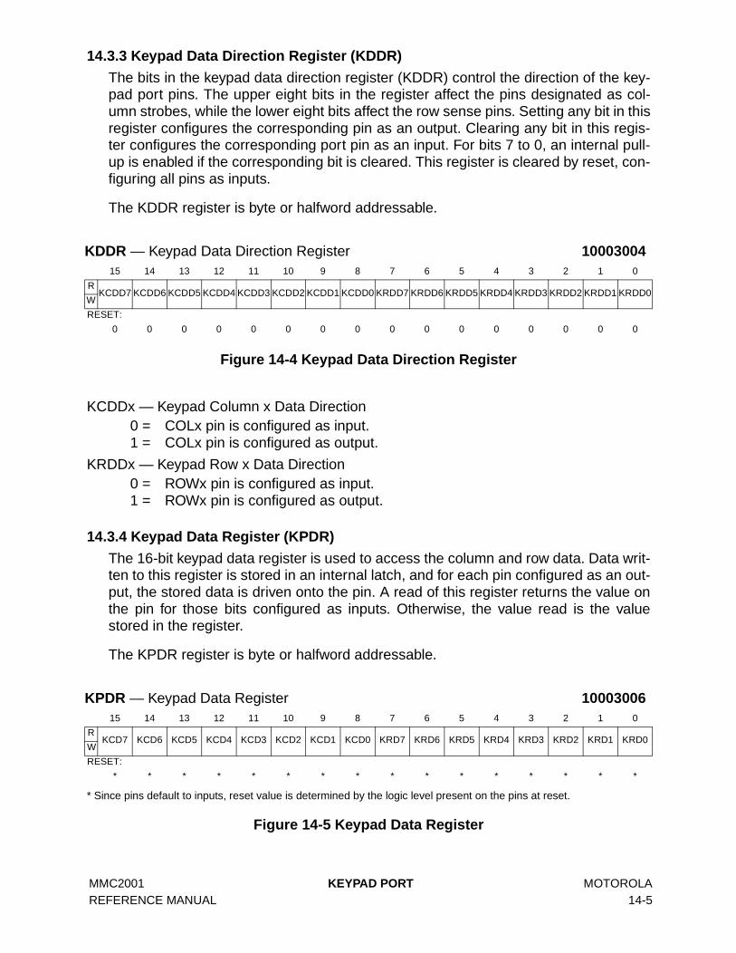
MMC2001 KEYPAD PORT MOTOROLA REFERENCE MANUAL 14-5
14.3.3 Keypad Data Direction Register (KDDR)
The bits in the keypad data direction register (KDDR) control the direction of the key-pad port pins. The upper eight bits in the register affect the pins designated as col-umn strobes, while the lower eight bits affect the row sense pins. Setting any bit in thisregister configures the corresponding pin as an output. Clearing any bit in this regis-ter configures the corresponding port pin as an input. For bits 7 to 0, an internal pull-up is enabled if the corresponding bit is cleared. This register is cleared by reset, con-figuring all pins as inputs.
The KDDR register is byte or halfword addressable.
Figure 14-4 Keypad Data Direction Register
KCDDx — Keypad Column x Data Direction 0 = COLx pin is configured as input. 1 = COLx pin is configured as output.
KRDDx — Keypad Row x Data Direction 0 = ROWx pin is configured as input.1 = ROWx pin is configured as output.
14.3.4 Keypad Data Register (KPDR)
The 16-bit keypad data register is used to access the column and row data. Data writ-ten to this register is stored in an internal latch, and for each pin configured as an out-put, the stored data is driven onto the pin. A read of this register returns the value onthe pin for those bits configured as inputs. Otherwise, the value read is the valuestored in the register.
The KPDR register is byte or halfword addressable.
* Since pins default to inputs, reset value is determined by the logic level present on the pins at reset.
Figure 14-5 Keypad Data Register
KDDR — Keypad Data Direction Register 1000300415 14 13 12 11 10 9 8 7 6 5 4 3 2 1 0
RKCDD7 KCDD6 KCDD5 KCDD4 KCDD3 KCDD2 KCDD1 KCDD0 KRDD7 KRDD6 KRDD5 KRDD4 KRDD3 KRDD2 KRDD1 KRDD0
W
RESET:
0 0 0 0 0 0 0 0 0 0 0 0 0 0 0 0
KPDR — Keypad Data Register 1000300615 14 13 12 11 10 9 8 7 6 5 4 3 2 1 0
RKCD7 KCD6 KCD5 KCD4 KCD3 KCD2 KCD1 KCD0 KRD7 KRD6 KRD5 KRD4 KRD3 KRD2 KRD1 KRD0
W
RESET:
* * * * * * * * * * * * * * * *

MOTOROLA KEYPAD PORT MMC2001 14-6 REFERENCE MANUAL
KCDx — Keypad Column x Data Bit
KRDx — Keypad Row x Data Bit
This register is not initialized by reset. Valid data should be written to this registerbefore any bits are configured as outputs.
14.4 Keypad Operation
The keypad port is designed to simplify the software task of scanning a keypadmatrix. With appropriate software support, the KPP is capable of detecting, debounc-ing, and decoding one or two keys pressed simultaneously in the keypad.
Logic in the KPP can detect a key press even while the processor is in one of the low-power standby modes. The KPP may generate a CPU interrupt any time a key pressor key release is detected. This interrupt can force the processor out of a low-powermode.
14.4.1 Keypad Matrix Construction
The keypad port is designed to interface to a keypad matrix which shorts the inter-secting row and column lines together whenever a key is depressed. The interface isnot optimized for other switch configurations.
14.4.2 Keypad Port Configuration
Software must initialize the keypad port for the size of the keypad matrix. Pins con-nected to the keypad columns should be configured as open-drain outputs. Pins con-nected to the keypad rows should be configured as inputs. On-chip pull-up resistorsare implemented for active keypad rows, as defined in SECTION 4 SIGNALDESCRIPTIONS.
Row inputs must also be enabled in the keypad control register to be active in theinterrupt generation circuit.
Discrete switches that are not part of the matrix may be connected to any unused rowinputs. The second terminal of the discrete switch is connected to ground. The hard-ware detects closures of these switches without the need for software polling.
14.4.3 Keypad Matrix Scanning
Keypad scanning is performed by a software loop that walks a zero across each ofthe keypad columns, reading the value on the rows at each step. The process isrepeated several times in succession, with the results of each pass optionally com-pared with those from the previous pass. When three or four consecutive scans yieldthe same key closures, a valid key press has been detected. Software can thendecode exactly which switch was depressed and pass the value up to the next highersoftware layer.
The basic debouncing period to be defined in the software routine can be controlledwith an internal timer. The basic period is the period between the scan of two consec-utive columns, so the debounce time between two consecutive scans of the wholematrix equals the number of columns multiplied by the basic period.

MMC2001 KEYPAD PORT MOTOROLA REFERENCE MANUAL 14-7
14.4.4 Keypad Standby
There is no need for the CPU to scan the keypad continually. Between key presses,the keypad can be left in a state that requires no software intervention until the nextkey press is detected. To place the keypad in a standby state, software writes all col-umn outputs low. Row inputs are left enabled. At this point the CPU can attend toother tasks or revert to a low-power standby mode. The keypad port will interrupt theCPU if any key is pressed.
Upon receiving a keypad interrupt, the CPU should set all the column strobes highand begin a normal keypad scanning routine to determine which key was pressed. Itis important that open-drain drivers be used when scanning to prevent a possible DCpath between power and ground through two or more switches.
14.4.5 Glitch Suppression on Keypad Inputs
A glitch suppression circuit qualifies the keypad inputs to prevent noise from inadvert-ently interrupting the CPU. The circuit is a four-state synchronizer clocked from a 256-Hz clock source. This clock must continue to run in any low-power mode for which thekeypad is a wake-up source, as the CPU interrupt is generated from the synchronizedinput. An interrupt is not generated until all four synchronizer stages have latched avalid key assertion, effectively filtering out any noise less than 16 ms in duration. Theinterrupt output is latched in an S-R latch and remains asserted until cleared by soft-ware. The set input of the latch is clocked on the rising edge.
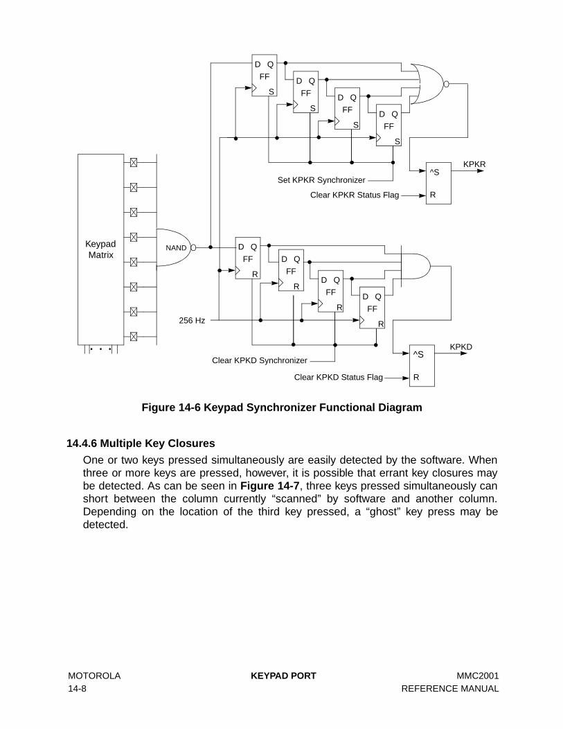
MOTOROLA KEYPAD PORT MMC2001 14-8 REFERENCE MANUAL
Figure 14-6 Keypad Synchronizer Functional Diagram
14.4.6 Multiple Key Closures
One or two keys pressed simultaneously are easily detected by the software. Whenthree or more keys are pressed, however, it is possible that errant key closures maybe detected. As can be seen in Figure 14-7, three keys pressed simultaneously canshort between the column currently “scanned” by software and another column.Depending on the location of the third key pressed, a “ghost” key press may bedetected.
Keypad
256 Hz
Matrix
. . .
FF
D Q
FF
D Q
FF
D Q
FF
D Q
^S
RClear KPKD Status Flag
NAND
R
R
R
R
KPKD
FF
D Q
FF
D Q
FF
D Q
FF
D Q
^S
R
S
S
S
S
KPKR
Clear KPKR Status Flag
Clear KPKD Synchronizer
Set KPKR Synchronizer

MMC2001 KEYPAD PORT MOTOROLA REFERENCE MANUAL 14-9
Figure 14-7 Decoding Wrong Three Key Presses
14.4.7 Typical Keypad Configuration and Scanning Sequence1. Configure keypad
a. Enable number of rows in keypad (KPCR[7:0]).b. Write zeros to KPDR[15:8].c. Configure keypad columns as open-drain (KPCR[15:8]).d. Configure columns as output, rows as input (KDDR[15:0]).e. Clear the KPKD status flag and synchronizer chain.f. Set the KDIE control bit, and clear the KRIE control bit (avoid false release
events).
(now in standby mode, awaiting a keypress...)
2. Keypress interrupt detected3. Begin keypad scanning routine
a. Disable keypad interrupts.b. Write ones to KPDR[15:8], setting column data to ones.c. Configure columns as totem-pole outputs.d. Configure columns as open-drain.e. Write a single column to zero, and write others to one.f. Sample row inputs and save data. Multiple key presses can be detected on a
single column. g. Repeat steps b to f for remaining columns. h. Return all columns to zero in preparation for standby mode.
Column PulledDown
Column not Pulled Down
Pulled Down Row
Pulled Down Row
Three RealKey Presses
Ghost KeyPress
The path of the zero pull downthat reaches the wrong row and sogenerates a ghost key press

MOTOROLA KEYPAD PORT MMC2001 14-10 REFERENCE MANUAL
i. Clear interrupt status bit(s) by writing to a one; set the KPKR synchronizer chain,clear the KPKD synchronizer chain.
j. Re-enable the appropriate keypad interrupt(s);KDIE to detect a key hold condition, orKRIE to detect a key release event.
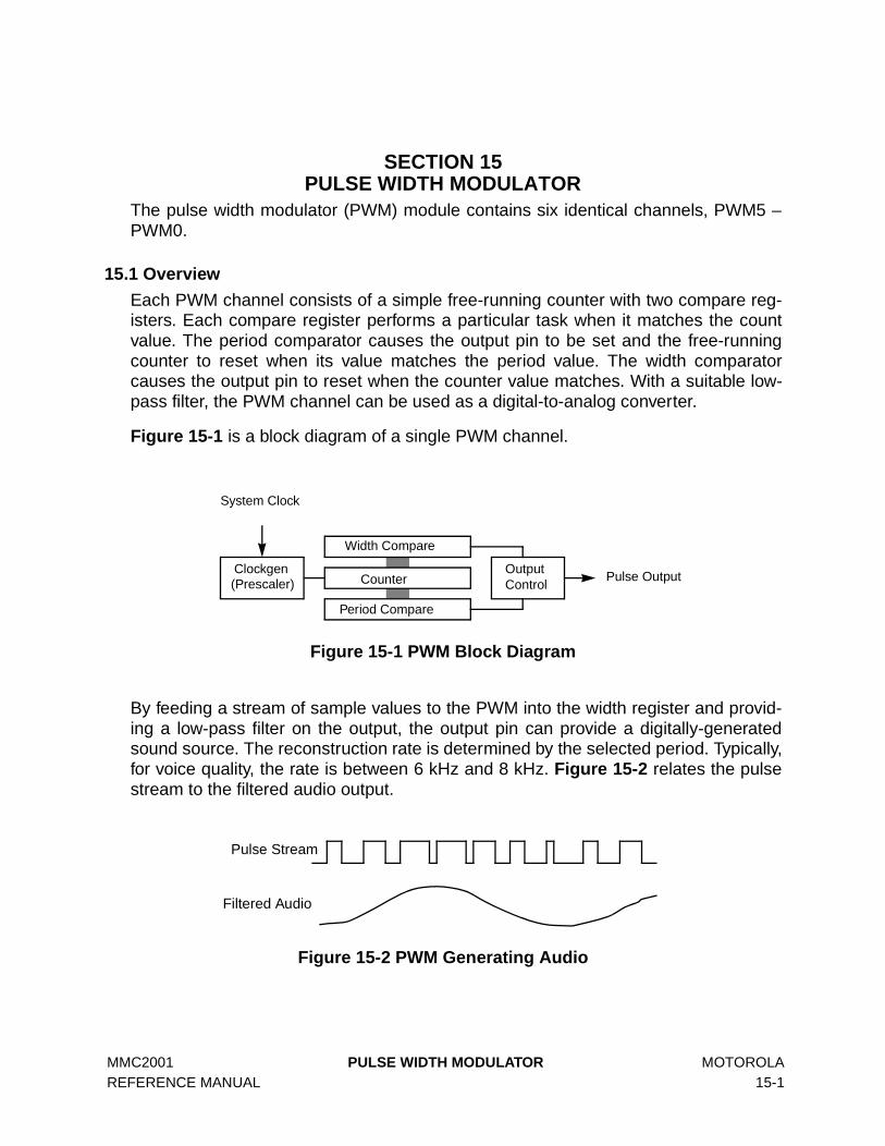
MMC2001 PULSE WIDTH MODULATOR MOTOROLA REFERENCE MANUAL 15-1
SECTION 15PULSE WIDTH MODULATOR
The pulse width modulator (PWM) module contains six identical channels, PWM5 –PWM0.
15.1 Overview
Each PWM channel consists of a simple free-running counter with two compare reg-isters. Each compare register performs a particular task when it matches the countvalue. The period comparator causes the output pin to be set and the free-runningcounter to reset when its value matches the period value. The width comparatorcauses the output pin to reset when the counter value matches. With a suitable low-pass filter, the PWM channel can be used as a digital-to-analog converter.
Figure 15-1 is a block diagram of a single PWM channel.
Figure 15-1 PWM Block Diagram
By feeding a stream of sample values to the PWM into the width register and provid-ing a low-pass filter on the output, the output pin can provide a digitally-generatedsound source. The reconstruction rate is determined by the selected period. Typically,for voice quality, the rate is between 6 kHz and 8 kHz. Figure 15-2 relates the pulsestream to the filtered audio output.
Figure 15-2 PWM Generating Audio
System Clock
Clockgen(Prescaler)
Width Compare
Counter
Period Compare
OutputControl
Pulse Output
Pulse Stream
Filtered Audio

MOTOROLA PULSE WIDTH MODULATOR MMC2001 15-2 REFERENCE MANUAL
The width and period registers are double-buffered so that a new value can be loadedfor the next cycle without disturbing the current cycle. At the beginning of each period,the contents of the buffer registers are loaded into the comparator for the next cycle.Sampled audio can be recreated by feeding a new sample value into the width regis-ter on each interrupt.
A single shared prescaler provides operating flexibility. Figure 15-3 describes itsfunctionality. The prescaler contains a variable divider that can divide the incomingclock by certain values between four and 65536.
Figure 15-3 PWM Prescaler
Each PWM channel can independently select a prescaler tap point. In addition, eachchannel provides a maskable interrupt request that can be asserted after each periodcompare event.
Channels can be used as periodic interrupt sources. In this case, the output pin asso-ciated with a channel can be used as a general-purpose I/O pin operating indepen-dently of the timing function.
15.2 PWM Programming Model
This section describes the registers and control bits in the PWM module. All registersreset to 0x0000 after reset.
These registers must be accessed with halfword accesses. Accesses other than half-word in size result in undefined activity.
DivideBy 4
DivideBy 2
DivideBy 2
DivideBy 4
DivideBy 4
DivideBy 8
DivideBy 8
DivideBy 4
PC
LKCLK
CLK SEL
SEL
HI_
RE
FC
LK
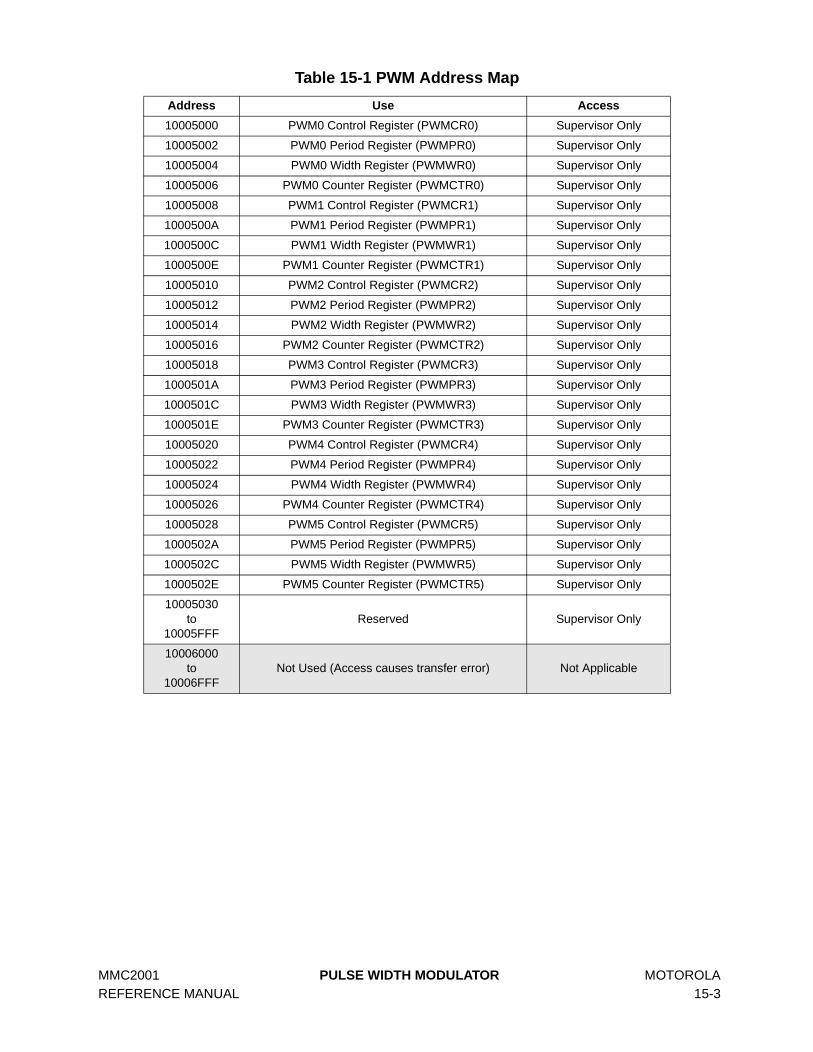
MMC2001 PULSE WIDTH MODULATOR MOTOROLA REFERENCE MANUAL 15-3
Table 15-1 PWM Address Map
Address Use Access
10005000 PWM0 Control Register (PWMCR0) Supervisor Only
10005002 PWM0 Period Register (PWMPR0) Supervisor Only
10005004 PWM0 Width Register (PWMWR0) Supervisor Only
10005006 PWM0 Counter Register (PWMCTR0) Supervisor Only
10005008 PWM1 Control Register (PWMCR1) Supervisor Only
1000500A PWM1 Period Register (PWMPR1) Supervisor Only
1000500C PWM1 Width Register (PWMWR1) Supervisor Only
1000500E PWM1 Counter Register (PWMCTR1) Supervisor Only
10005010 PWM2 Control Register (PWMCR2) Supervisor Only
10005012 PWM2 Period Register (PWMPR2) Supervisor Only
10005014 PWM2 Width Register (PWMWR2) Supervisor Only
10005016 PWM2 Counter Register (PWMCTR2) Supervisor Only
10005018 PWM3 Control Register (PWMCR3) Supervisor Only
1000501A PWM3 Period Register (PWMPR3) Supervisor Only
1000501C PWM3 Width Register (PWMWR3) Supervisor Only
1000501E PWM3 Counter Register (PWMCTR3) Supervisor Only
10005020 PWM4 Control Register (PWMCR4) Supervisor Only
10005022 PWM4 Period Register (PWMPR4) Supervisor Only
10005024 PWM4 Width Register (PWMWR4) Supervisor Only
10005026 PWM4 Counter Register (PWMCTR4) Supervisor Only
10005028 PWM5 Control Register (PWMCR5) Supervisor Only
1000502A PWM5 Period Register (PWMPR5) Supervisor Only
1000502C PWM5 Width Register (PWMWR5) Supervisor Only
1000502E PWM5 Counter Register (PWMCTR5) Supervisor Only
10005030to
10005FFFReserved Supervisor Only
10006000to
10006FFFNot Used (Access causes transfer error) Not Applicable
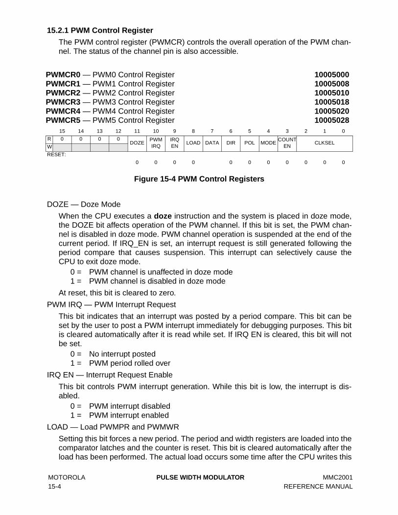
MOTOROLA PULSE WIDTH MODULATOR MMC2001 15-4 REFERENCE MANUAL
15.2.1 PWM Control Register
The PWM control register (PWMCR) controls the overall operation of the PWM chan-nel. The status of the channel pin is also accessible.
Figure 15-4 PWM Control Registers
DOZE — Doze Mode
When the CPU executes a doze instruction and the system is placed in doze mode,the DOZE bit affects operation of the PWM channel. If this bit is set, the PWM chan-nel is disabled in doze mode. PWM channel operation is suspended at the end of thecurrent period. If IRQ_EN is set, an interrupt request is still generated following theperiod compare that causes suspension. This interrupt can selectively cause theCPU to exit doze mode.
0 = PWM channel is unaffected in doze mode1 = PWM channel is disabled in doze mode
At reset, this bit is cleared to zero.
PWM IRQ — PWM Interrupt Request
This bit indicates that an interrupt was posted by a period compare. This bit can beset by the user to post a PWM interrupt immediately for debugging purposes. This bitis cleared automatically after it is read while set. If IRQ EN is cleared, this bit will notbe set.
0 = No interrupt posted1 = PWM period rolled over
IRQ EN — Interrupt Request Enable
This bit controls PWM interrupt generation. While this bit is low, the interrupt is dis-abled.
0 = PWM interrupt disabled1 = PWM interrupt enabled
LOAD — Load PWMPR and PWMWR
Setting this bit forces a new period. The period and width registers are loaded into thecomparator latches and the counter is reset. This bit is cleared automatically after theload has been performed. The actual load occurs some time after the CPU writes this
PWMCR0 — PWM0 Control Register 10005000PWMCR1 — PWM1 Control Register 10005008PWMCR2 — PWM2 Control Register 10005010PWMCR3 — PWM3 Control Register 10005018PWMCR4 — PWM4 Control Register 10005020PWMCR5 — PWM5 Control Register 10005028
15 14 13 12 11 10 9 8 7 6 5 4 3 2 1 0
R 0 0 0 0DOZE
PWMIRQ
IRQEN
LOAD DATA DIR POL MODECOUNT
ENCLKSEL
W
RESET:
0 0 0 0 0 0 0 0 0 0 0

MMC2001 PULSE WIDTH MODULATOR MOTOROLA REFERENCE MANUAL 15-5
bit, as the load occurs on the next rising PCLK edge following internal synchroniza-tion. Forcing a load of the comparator latches and counter in this manner must bedone with caution to avoid unexpected pin behavior.
DATA — PWM Data
This bit indicates or controls the current state of the PWM pin. When the pin is config-ured as a general-purpose output, the logical value written to this bit is used to drivethe pin. When the pin is configured as a general-purpose input, the pin value isreflected by this bit. When the pin is configured in PWM mode, the bit reflects thevalue being driven on the pin by the PWM logic.
DIR — Direction
This bit controls the direction of the pin when used as a GPIO pin. This bit has noeffect when MODE indicates PWM mode.
0 = Pin is an input pin1 = Pin is an output pin
POL — Polarity
This bit controls the polarity of the pin when used as a PWM output pin. Normally, theoutput pin is set high at period boundaries and goes low when a width compare eventoccurs.
This bit is ignored if the pin is being used as a GPIO pin.0 = Normal PWM polarity1 = Inverted PWM polarity
MODE — PWM Mode
This bit selects whether the PWM pin is used for GPIO or for the PWM function.0 = General-purpose I/O mode1 = PWM mode
COUNT EN — Counter Enable
This bit enables or disables the PWM counter. The counter is actually enabled or dis-abled some time after the CPU writes this bit. It is enabled on the next rising PCLKedge following internal synchronization. If running, the counter is disabled followingthe next period match.
0 = PWM disabled. While disabled, the counter is in a low-power mode and doesnot count. The following events occur:
When the output pin is configured to operate in PWM mode (MODE = 1), theoutput pin is forced to the setting of the POL bit.
The counter is reset to 00 and frozen.
The contents of the width and period registers are loaded into the compara-tors.
The comparators are disabled.
If the counter has been running, and the actual disable occurs at the occur-rence of a period match, an interrupt request may still be generated, eventhough the counter is being disabled. To prevent this, write the interruptenable control bit (IRQ_EN) to zero when disabling the counter.

MOTOROLA PULSE WIDTH MODULATOR MMC2001 15-6 REFERENCE MANUAL
1 = PWM is enabled and begins a new period. The following events occur:
The output pin changes state to start a new period (if width != 0 andperiod != 0 and width < period)
The counter is released and begins counting
The comparators are enabled
The PWM IRQ bit is set, indicating the start of a new period if IRQ EN is set.
CLK SEL — Clock Select
These bits select the output of the divider chain.
15.2.2 PWM Period Register
The PWM period register (PWMPR) controls the period of the PWM by defining thenumber of PCLKs in the period. When the counter value matches the value in thisregister, an interrupt is posted and the counter is reset to start another period.
Figure 15-5 PWM Period Registers
PERIOD — Pulse PeriodThis is the value that causes the counter to be reset. There is one special case. WhenPERIOD = 0, the output is never set high (0% duty cycle). In this case, the compara-tor is loaded and the counter reset on every PCLK. In addition, if enabled, an interruptrequest is generated on every PCLK.
Table 15-2 CLK SEL Field Settings
Value Divide By
000 4
001 8
010 16
011 64
100 256
101 2048
110 16384
111 65536
PWMPR0 — PWM0 Period Register 10005002PWMPR1 — PWM1 Period Register 1000500APWMPR2 — PWM2 Period Register 10005012PWMPR3 — PWM3 Period Register 1000501APWMPR4 — PWM4 Period Register 10005022PWMPR5 — PWM5 Period Register 1000502A
15 14 13 12 11 10 9 8 7 6 5 4 3 2 1 0
R 0 0 0 0 0 0PERIOD
W
RESET:
0 0 0 0 0 0 0 0 0 0

MMC2001 PULSE WIDTH MODULATOR MOTOROLA REFERENCE MANUAL 15-7
15.2.3 PWM Width Register
The PWM width register (PWMWR) defines the width of the pulse in PCLKs. Whenthe counter matches the value in this register, the output is reset for the duration ofthe period. Note that if the value in this register is not less than the period register, theoutput will never be reset, resulting in a 100% duty cycle.
Figure 15-6 PWM Width Registers
WIDTH — Pulse Width
When the counter reaches the value in this register, the output is reset.
15.2.4 PWM Counter Register
The read-only PWM counter register (PWMCTR) holds the current count value. It canbe read at any time without disturbing the counter.
Figure 15-7 PWM Count Registers
COUNT — Count Value
This is the current count value.
PWMWR0 — PWM0 Width Register 10005004PWMWR1 — PWM1 Width Register 1000500CPWMWR2 — PWM2 Width Register 10005014PWMWR3 — PWM3 Width Register 1000501CPWMWR4 — PWM4 Width Register 10005024PWMWR5 — PWM5 Width Register 1000502C
15 14 13 12 11 10 9 8 7 6 5 4 3 2 1 0
R 0 0 0 0 0 0WIDTH
W
RESET:
0 0 0 0 0 0 0 0 0 0
PWMCTR0 — PWM0 Counter Register 10005006PWMCTR1 — PWM1 Counter Register 1000500EPWMCTR2 — PWM2 Counter Register 10005016PWMCTR3 — PWM3 Counter Register 1000501EPWMCTR4 — PWM4 Counter Register 10005026PWMCTR5 — PWM5 Counter Register 1000502E
15 14 13 12 11 10 9 8 7 6 5 4 3 2 1 0
R 0 0 0 0 0 0COUNT
W
RESET:
0 0 0 0 0 0 0 0 0 0

MOTOROLA PULSE WIDTH MODULATOR MMC2001 15-8 REFERENCE MANUAL
15.3 PWM Operating Range
Table 15-3 shows the operating range and resolution of the PWM with a 16-MHzHI_REFCLK. The minimum period range assumes a value of two in the period regis-ter, while the maximum assumes a value of 256.
15.4 PWM Operation in Low-Power System Modes
Table 15-4 summarizes PWM operation in the different low-power modes.
In most modes, the PWM operates as long as a clock is available. In doze mode, thePWM channels may be selectively disabled, depending on the value of the DOZEcontrol bit. PWM channel operation will be suspended at the end of the currentperiod. In stop mode, the PWM halts immediately (due to halting of system clocks)and forgets the state of any period (the state machine is reset, and the shift register iscleared). It is assumed that when stop is initiated, the channels have been disabled.
Table 15-3 PWM Range at 16 MHz
Divide By Approximate Period
Range at 16 MHzResolution at
16 MHz
4 0.5 µs – 256 µs .25 µs
8 1 µs – 512 µs .5 µs
16 2 µs – 1 ms 1 µs
64 8 µs – 4.1 ms 4 µs
256 32 µs – 16.5 ms 16 µs
2048 256 µs – 65.6 ms 128 µs
16384 2 ms – 1 s 1 ms
65536 8.2 ms – 4 s 4.1 ms
Table 15-4 PWM Low-Power Mode Operation
Mode Operation
Normal Runs whenever enabled
Wait Runs whenever enabled
DozeIf DOZE is set (in PWM control register), then disabled.
Stop Disabled

MMC2001 OnCE™ DEBUG MODULE MOTOROLA REFERENCE MANUAL 16-1
SECTION 16OnCE™ DEBUG MODULE
16.1 Overview
The on-chip emulation (OnCE™) circuitry provides a simple, inexpensive debugginginterface that allows external access to the processor’s internal registers and to mem-ory/peripherals. OnCE capabilities are controlled through a serial interface, mappedonto a JTAG test access port (TAP) protocol. Figure 16-1 shows the components ofthe OnCE circuitry.
Figure 16-1 OnCE Block Diagram
The interface to the OnCE controller and its resources is based on the TAP definedfor JTAG in the IEEE-1149.1a-1993 standard.
16.2 Operation
An instruction is scanned into the OnCE module through the serial interface and thendecoded. Data may then be scanned in and used to update a register or resource ona write to the resource, or data associated with a resource may be scanned out for aread of the resource.
PSTATATTR
ADDR
...
TDO
TMS
TDI
TCK
Breakpoint andTrace Logic
OnCE Controller
andSerial
Interface
BreakpointRegisters
andComparators
PCFIFO
Pipeline Information
TRST
BRKRQ
DBGRQ
DEBUG
DBGACK
IDR
DE
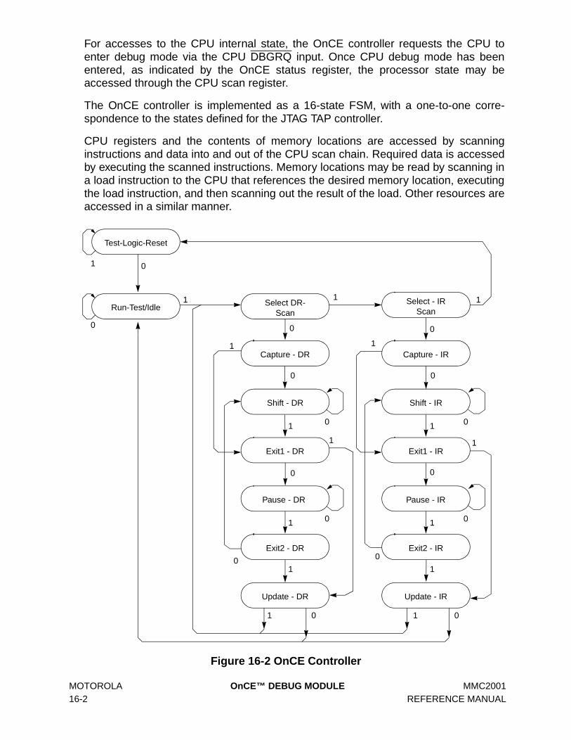
MOTOROLA OnCE™ DEBUG MODULE MMC2001 16-2 REFERENCE MANUAL
For accesses to the CPU internal state, the OnCE controller requests the CPU toenter debug mode via the CPU DBGRQ input. Once CPU debug mode has beenentered, as indicated by the OnCE status register, the processor state may beaccessed through the CPU scan register.
The OnCE controller is implemented as a 16-state FSM, with a one-to-one corre-spondence to the states defined for the JTAG TAP controller.
CPU registers and the contents of memory locations are accessed by scanninginstructions and data into and out of the CPU scan chain. Required data is accessedby executing the scanned instructions. Memory locations may be read by scanning ina load instruction to the CPU that references the desired memory location, executingthe load instruction, and then scanning out the result of the load. Other resources areaccessed in a similar manner.
Figure 16-2 OnCE Controller
Capture - DR
Shift - DR
Exit1 - DR
Pause - DR
Exit2 - DR
Update - DR
Select - IRScan
Capture - IR
Shift - IR
Exit1 - IR
Pause - IR
Exit2 - IR
Update - IR
Select DR-Scan
Run-Test/Idle
Test-Logic-Reset
1
0
1
1 1
1
1
1
1
1
1
1
1
1
1
1
1
0 0
00
0 0
00
00
0
0
00
0
MMC2001 OnCE™ DEBUG MODULE MOTOROLA REFERENCE MANUAL 16-3
Resources contained in the OnCE module that do not require the CPU to be haltedfor access may be controlled while the CPU is executing and do not interfere with nor-mal processor execution. Accesses to certain resources, such as the PC FIFO andthe count registers, while not part of the CPU, may require the CPU to be stopped toallow access to avoid synchronization hazards. If it is known that the CPU clock isenabled and running no slower than the TCK input, there is sufficient synchronizationperformed to allow reads but not writes of these specific resources. Debug firmwaremay ensure that it is safe to access these resources by reading the OSR to determinethe state of the CPU prior to access. All other cases require the CPU to be in thedebug state for deterministic operation.
16.3 OnCE Pins
The following paragraphs describe the pins associated with the OnCE controller andserial interface component.
The OnCE pin interface is used to transfer OnCE instructions and data to the OnCEcontrol block. Depending on the particular resource being accessed, the CPU mayneed to be placed in debug mode. For resources outside of the CPU block and con-tained in the OnCE block, the processor is not disturbed and may continue execution.If a processor resource is required, the OnCE controller may assert a debug request(DBGRQ) to the CPU. This causes the CPU to finish the instruction being executed,save the instruction pipeline information, enter debug mode, and wait for further com-mands. Asserting DBGRQ causes the device to exit stop, doze, or wait mode.
16.3.1 Debug Serial Input (TDI)
Data and commands are provided to the OnCE controller through the TDI pin. Data islatched on the rising edge of the TCK serial clock. Data is shifted into the OnCE serialport least significant bit (LSB) first.
16.3.2 Debug Serial Clock (TCK)
The TCK pin supplies the serial clock to the OnCE control block. The serial clock pro-vides pulses required to shift data and commands into and out of the OnCE serialport. (Data is clocked into the OnCE on the rising edge and is clocked out of theOnCE serial port on the falling edge.) The debug serial clock frequency must be nogreater than 50% of the processor clock frequency.
16.3.3 Debug Serial Output (TDO)
Serial data is read from the OnCE block through the TDO pin. Data is always shiftedout the OnCE serial port LSB first. Data is clocked out of the OnCE serial port on thefalling edge of TCK. TDO is three-stateable and is actively driven in the shift-IR andshift-DR controller states. TDO changes on the falling edge of TCK.
16.3.4 Debug Mode Select (TMS)
The debug mode select input is used to cycle through states in the OnCE debug con-troller. Toggling the TMS pin while clocking with TCK controls the transitions throughthe TAP state controller.

MOTOROLA OnCE™ DEBUG MODULE MMC2001 16-4 REFERENCE MANUAL
16.3.5 Test Reset (TRST)
The test reset input is used to reset the OnCE controller externally by placing theOnCE control logic in a test logic reset state. OnCE operation is disabled in the resetcontroller and reserved states.
16.3.6 Debug Event (DE)
The debug event (DE) pin is a bidirectional open drain pin. As an input, DE provides afast means of entering debug mode from an external command controller. As an out-put, this pin provides a fast means of acknowledging debug mode entry to an externalcommand controller.
The assertion of this pin by a command controller causes the CPU to finish the cur-rent instruction being executed, save the instruction pipeline information, enter debugmode, and wait for commands to be entered from the TDI line. If DE was used toenter debug mode, then DE must be negated after the OnCE responds with anacknowledgment and before sending the first OnCE command.
The assertion of this pin by the CPU acknowledges that it has entered debug modeand is waiting for commands to be entered from the TDI line.
16.4 OnCE Controller and Serial Interface
Figure 16-3 is a block diagram of the OnCE controller and serial interface.
Figure 16-3 OnCE Controller and Serial Interface
OnCE Command RegisterTDI
TCK
Status and ControlRegisters
TDO
Mode Select
OnCE Decoder
ISBKPT
ISDR
ISTRACE
Register WriteRegister Read
.
.
..
.
TAP
TMS
CPU Control/Status
Controller

MMC2001 OnCE™ DEBUG MODULE MOTOROLA REFERENCE MANUAL 16-5
The OnCE controller and serial interface contain the following blocks: OnCE TAP con-troller, the OnCE command register, OnCE decoder, and the OnCE control and statusregisters.
The OnCE command register acts as the IR for the TAP controller. All other OnCEresources are treated as data registers (DR) by the TAP controller. The commandregister is loaded by serially shifting in commands during the TAP controller shift-IRstate, and is loaded during the update-IR state. The command register selects aOnCE resource to be accessed as a data register (DR) during the TAP controller cap-ture-DR, shift-DR and update-DR states.
16.5 OnCE Interface Signals
The following paragraphs describe the OnCE interface signals to other internal blocksassociated with the OnCE controller. These signals are not available externally, anddescriptions are provided to improve understanding of OnCE operation.
16.5.1 Internal Debug Request Input (IDR)
The internal debug request input is a hardware signal which is used in some imple-mentations to force an immediate debug request to the CPU. If present and enabled,it functions in an identical manner to the control function provided by the DR controlbit in the OnCE control register (OCR). This input is maskable by a control bit in OCR.
16.5.2 CPU Debug Request (DBGRQ)
The DBGRQ signal is asserted by the OnCE control logic to request the CPU to enterthe debug state. It may be asserted for a number of different conditions. Assertion ofthis signal causes the CPU to finish the current instruction being executed, save theinstruction pipeline information, enter debug mode, and wait for further commands.Asserting DBGRQ causes the device to exit stop, doze, or wait mode.
16.5.3 CPU Debug Acknowledge (DBGACK)
The CPU asserts the DBGACK signal upon entering the debug state. This signal ispart of the handshake mechanism between the OnCE control logic and the CPU.
16.5.4 CPU Breakpoint Request (BRKRQ)
The BRKRQ signal is asserted by the OnCE control logic to signal that a breakpointcondition has occurred for the current CPU bus access.
16.5.5 CPU Address, Attributes (ADDR, ATTR)
The CPU address and attribute information may be used in the memory breakpointlogic to qualify memory breakpoints with access address and cycle type information.
16.5.6 CPU Status (PSTAT)
The trace logic uses the CPU PSTAT signals to qualify trace count decrements withspecific CPU activity.
MOTOROLA OnCE™ DEBUG MODULE MMC2001 16-6 REFERENCE MANUAL
16.5.7 OnCE Debug Output (DEBUG)
The OnCE debug output (DEBUG) is used to indicate to on-chip resources that adebug session is in progress. Peripherals and other units may use this signal to mod-ify normal operation for the duration of a debug session. This may involve the CPUexecuting a sequence of instructions solely for the purpose of visibility/system control.These instructions are not part of the normal instruction stream the CPU would haveexecuted had it not been placed in debug mode.
This signal is asserted the first time the CPU enters the debug state and remainsasserted until the CPU is released by a write to the OnCE command register with theGO and EX bits set, and a register specified as either “No register selected” or theCPUSCR. This signal remains asserted even though the CPU may enter and exit thedebug state for each instruction executed under control of the OnCE controller. See16.6.1 OnCE Command Register (OCMR) for more information on the function ofthe GO and EX bits.
16.6 OnCE Controller Registers
This section describes the OnCE controller registers:
• OnCE Command Register (OCMR)• OnCE Control Register (OCR)• OnCE Status Register (OSR)
All OnCE registers are addressed by means of the RS field in the OMCR, as shown inTable 16-1.
Other OnCE registers are described in 16.8 Memory Breakpoint Logic and 16.9OnCE Trace Logic.
16.6.1 OnCE Command Register (OCMR)
The OnCE command register (OCMR) is an 8-bit shift register that receives its serialdata from the TDI pin. This register corresponds to the JTAG IR, and is loaded whenthe update-IR TAP controller state is entered. It holds the 8-bit commands shifted induring the shift-IR controller state to be used as input for the OnCE decoder. TheOCMR contains fields for controlling access to a OnCE resource, as well as control-ling single-step operation, and exit from OnCE mode.
Although the OCMR is updated during the update-IR TAP controller state, the corre-sponding resource is accessed in the DR scan sequence of the TAP controller, andas such, the update-DR state must be transitioned through in order for an access tooccur. In addition, the update-DR state must also be transitioned through in order forthe single-step and/or exit functionality to be performed, even though the commandappears to have no data resource requirement associated with it.
The command register is shown in Figure 16-4.

MMC2001 OnCE™ DEBUG MODULE MOTOROLA REFERENCE MANUAL 16-7
Figure 16-4 OnCE Command Register
R/W — Read/Write CommandThe R/W bit specifies the direction of data transfer.
0 = Write the data associated with the command into the register specified bythe RS field.
1 = Read the data contained in the register specified by the RS field.
GO — Go CommandWhen the GO bit is set, the device executes the instruction that resides in the IR reg-ister in the CPUSCR. To execute the instruction, the processor leaves debug mode,executes the instruction, and if the EX bit is cleared, returns to debug mode immedi-ately after executing the instruction. The processor resumes normal operation if theEX bit is set. The GO command is executed only if the operation is a read/write toeither CPUSCR or “No register selected”. Otherwise, the GO bit is ignored. The pro-cessor leaves debug mode after the TAP controller update-DR state is entered.
0 = Inactive (no action taken)1 = Execute instruction in IR
EX — Exit CommandWhen the EX bit is set, the processor leaves debug mode and resumes normal oper-ation until another debug request is generated. The exit command is executed only ifthe Go command is issued, and the operation is a read/write to CPUSCR or read/write to “No register selected”. Otherwise the EX bit is ignored. The processor exitsdebug mode after the TAP controller update-DR state is entered.
0 = Remain in debug mode1 = Leave debug mode
RS — Register Select The register select bits define the source or destination register for the read or writeoperation, respectively. Table 16-1 shows OnCE register addresses.
OCMR — OnCE Command Register
BIT 7 6 5 4 3 2 1 BIT 0R/W GO EX RS

MOTOROLA OnCE™ DEBUG MODULE MMC2001 16-8 REFERENCE MANUAL
16.6.2 OnCE Control Register (OCR)
The OnCE control register (OCR) is a 32-bit register used to select the events that willput the device in debug mode and to enable or disable sections of the OnCE logic.The control bits are read/write.
Figure 16-5 OnCE Control Register
Table 16-1 OnCE Register Addressing
RS Register Selected
00000 Reserved
00001 Reserved
00010 Reserved
00011 Trace Counter (OTC)
00100 Memory Breakpoint Counter A (MBCA)
00101 Memory Breakpoint Counter B (MBCB)
00110 Program Counter FIFO and Increment Counter
00111 Breakpoint Address Base Register A (BABA)
01000 Breakpoint Address Base Register B (BABB)
01001 Breakpoint Address Mask Register A (BAMA)
01010 Breakpoint Address Mask Register B (BAMB)
01011 CPU Scan Register (CPUSCR)
01100 No Register Selected (Bypass)
01101 OnCE Control Register (OCR)
01110 OnCE Status Register (OSR)
01111 Reserved (Factory Test Control Register — do not access)
10000 Reserved (MEM_BIST, do not access)
10001 – 10110 Reserved (Bypass, do not access)
10111 Reserved (LSRL, do not access)
11000 – 11110 Reserved (Bypass, do not access)
11111 Bypass
OCR — OnCE Control Register31 30 29 28 27 26 25 24 23 22 21 20 19 18 17 16
R 0 0 0 0 0 0 0 0 0 0 0 0 0 0SQC
W
RESET:
0 0 0 0 0 0 0 0 0 0 0 0 0 0 0 0
15 14 13 12 11 10 9 8 7 6 5 4 3 2 1 0
RDR IDRE TME FRZC RCB BCB RCA BCA
W
RESET:
0 0 0 0 0 0 0 0 0 0 0 0 0 0 0 0

MMC2001 OnCE™ DEBUG MODULE MOTOROLA REFERENCE MANUAL 16-9
SQC — Sequential ControlThe SQC field allows memory breakpoint B and trace occurrences to be suspendeduntil a qualifying event occurs. This field is cleared on test logic reset.
DR — CPU Debug Request ControlThis control bit is used to request the CPU to enter debug mode unconditionally. TheCPU indicates that debug mode has been entered via the PM bits in the OnCE statusregister. Once the CPU enters debug mode, it returns there even with a write to theOCMR with GO and EX set until the DR bit is cleared. This bit is cleared on test logicreset.
IDRE — Internal Debug Request EnableThis control bit is used to enable internally generated debug requests. The internaldebug request input to the OnCE control logic (IDR) may not be used in all implemen-tations. In some implementations, the IDR control input may be connected and usedas an additional hardware debug request. This bit is cleared on test logic reset.
0 = Disable IDR input operation1 = Enable IDR input operation
TME — Trace Mode EnableThe TME control bit enables the OnCE trace mode operation (see 16.9 OnCE TraceLogic). This bit is cleared on test logic reset. Trace operation is also affected by theSQC field described above.
0 = Disable trace operation1 = Enable trace operation
Table 16-2 Sequential Control Field Settings
SQC[1:0] Meaning
00Disable sequential control operation. Memory breakpoints and trace operation are unaf-fected by this field.
01
Suspend normal trace counter operation until a breakpoint condition occurs for memory breakpoint B. If this mode is selected, memory breakpoint B occurrences no longer cause a breakpoint request to be generated. Instead, trace counter comparisons are suspended until the first memory breakpoint B occurrence. After the first memory breakpoint B occur-rence, trace counter control is released to perform normally (assuming TME is set). This allows a sequence of breakpoint conditions to be specified prior to trace counting.
10
Qualify memory breakpoint B matches with a breakpoint occurrence for memory break-point A. If this bit is set, memory breakpoint A occurrences no longer cause a breakpoint request to be generated. Instead, memory breakpoint B comparisons are suspended until the first memory breakpoint A occurrence. After the first memory breakpoint A occur-rence, memory breakpoint B is enabled to perform normally. This allows a sequence of breakpoint conditions to be specified.
11
Combine the qualifications specified by the 01 and 10 encodings of this field. In this mode, no breakpoint requests are generated, and trace count operation is enabled (if TME is set) once a memory breakpoint B occurrence follows a memory breakpoint A occurrence.

MOTOROLA OnCE™ DEBUG MODULE MMC2001 16-10 REFERENCE MANUAL
FRZC — Freeze ControlThis control bit is used in conjunction with memory breakpoint B registers to selectbetween asserting a breakpoint condition when a memory breakpoint B occurs, orfreezing the PC FIFO from further updates when memory breakpoint B occurs whileallowing the CPU to continue execution. The PC FIFO remains frozen until the FRZObit in the OSR is cleared.
0 = Memory breakpoint B occurrence causes assertion of a breakpoint condition1 = Memory breakpoint B occurrence causes a freeze of PC FIFO from further
updates and no breakpoint assertion
RCB, RCA — Memory Breakpoint B, A Range Control These control bits condition enabled memory breakpoints. They condition whethermemory breakpoint matches will occur when a memory address falls either within therange defined by memory base address and mask, or outside the range.
0 = Condition breakpoint on access within range1 = Condition breakpoint on access outside of range
BCB, BCA — Memory Breakpoint B, A Control These control bits enable memory breakpoints and qualify the access attributes toselect whether the breakpoint match will be recognized for read, write, or instructionfetch (program space) accesses. These bits are cleared on test logic reset. See Table16-3 for the definition of the BCA and BCB fields.
Table 16-3 Memory Breakpoint Control Field Settings
BC4 BC3 BC2 BC1 BC0 Description0 0 0 0 0 Breakpoint disabled
0 0 0 0 1 Qualify match with any access0 0 0 1 0 Qualify match with any instruction access0 0 0 1 1 Qualify match with any data access
0 0 1 0 0 Qualify match with any change of flow instruction access0 0 1 0 1 Qualify match with any data write0 0 1 1 0 Qualify match with any data read
0 0 1 1 1 Reserved0 1 x x x Reserved1 0 0 0 0 Reserved
1 0 0 0 1 Qualify match with any user access1 0 0 1 0 Qualify match with any user instruction access1 0 0 1 1 Qualify match with any user data access
1 0 1 0 0 Qualify match with any user change of flow access1 0 1 0 1 Qualify match with any user data write1 0 1 1 0 Qualify match with any user data read
1 0 1 1 1 Reserved1 1 0 0 0 Reserved1 1 0 0 1 Qualify match with any supervisor access
1 1 0 1 0 Qualify match with any supervisor instruction access1 1 0 1 1 Qualify match with any supervisor data access1 1 1 0 0 Qualify match with any supervisor change of flow access
1 1 1 0 1 Qualify match with any supervisor data write1 1 1 1 0 Qualify match with any supervisor data read1 1 1 1 1 Reserved

MMC2001 OnCE™ DEBUG MODULE MOTOROLA REFERENCE MANUAL 16-11
16.6.3 OnCE Status Register (OSR)
The OnCE status register (OSR) is a 16-bit register used to indicate the reason(s)that debug mode was entered and the current operating mode of the CPU. These sta-tus bits are read only.
Figure 16-6 OnCE Status Register
HDRO — Hardware Debug Request Occurrence This read-only status bit is set when the processor enters debug mode as a result ofa hardware debug request from the IDR signal or the DE pin. This bit is cleared ontest logic reset or when debug mode is exited with the GO and EX bits set.
DRO — Debug Request OccurrenceThis read-only status bit is set when the processor enters debug mode and the debugrequest (DR) control bit in the OnCE control register is set. This bit is cleared on testlogic reset or when debug mode is exited with the GO and EX bits set.
MBO — Memory Breakpoint OccurrenceThis read-only status bit is set when a memory breakpoint request has been issued tothe CPU via the BRKRQ input and the CPU enters debug mode. In some situationsinvolving breakpoint requests on instruction prefetches, the CPU may discard therequest along with the prefetch. In this case, this bit may become set due to the CPUentering debug mode for another reason. This bit is cleared on test logic reset orwhen debug mode is exited with the GO and EX bits set.
SWO — Software Debug OccurrenceThis read-only status bit is set when the processor enters debug mode of operationas a result of the execution of the bkpt instruction. This bit is cleared on test logicreset or when debug mode is exited with the GO and EX bits set.
TO — Trace Count OccurrenceThis read-only status bit is set when the trace counter reaches zero with the tracemode enabled and the CPU enters debug mode. This bit is cleared on test logic resetor when debug mode is exited with the GO and EX bits set.
FRZO — FIFO Freeze OccurrenceThis read-only status bit is set when a FIFO freeze occurs. This bit is cleared on testlogic reset or when debug mode is exited with the GO and EX bits set.
SQB — Sequential Breakpoint B Arm OccurrenceThis read-only status bit is set when sequential operation is enabled and a memorybreakpoint B event has occurred to enable trace counter operation. This bit is clearedon test logic reset or when debug mode is exited with the GO and EX bits set.
OSR — OnCE Status Register 15 14 13 12 11 10 9 8 7 6 5 4 3 2 1 0
R 0 0 0 0 0 0 HDRO DRO MBO SWO TO FRZO SQB SQA PM
W
RESET:
0 0 0 0 0 0 0 0 0 0

MOTOROLA OnCE™ DEBUG MODULE MMC2001 16-12 REFERENCE MANUAL
SQA — Sequential Breakpoint A Arm OccurrenceThis read-only status bit is set when sequential operation is enabled and a memorybreakpoint A event has occurred to enable memory breakpoint B operation. This bit iscleared on test logic reset or when debug mode is exited with the GO and EX bits set.
PM — Processor ModeThese status bits indicate the processor operating mode. They allow coordination ofthe OnCE controller with the CPU to synchronize the two.
16.7 OnCE Decoder (ODEC)
The OnCE decoder (ODEC) receives as input the 8-bit command from the OCMRand status signals from the processor. The ODEC generates all the strobes requiredfor reading and writing the selected OnCE registers.
16.8 Memory Breakpoint Logic
Memory breakpoints can be set for a particular memory location or on accesseswithin an address range. The breakpoint logic contains an input latch for addresses,registers that store the base address and address mask, comparators, attribute qual-ifiers, and a breakpoint counter. Figure 16-7 illustrates the basic functionality of theOnCE memory breakpoint logic. This logic is duplicated to provide two independentbreakpoint resources.
Address comparators can be used to determine where a program may be getting lostor when data is being written to areas which should not be written. They are also use-ful in halting a program at a specific point to examine or change registers or memory.Using address comparators to set breakpoints enables the user to set breakpoints inRAM or ROM in any operating mode. Memory accesses are monitored according tothe contents of the OCR.
Table 16-4 Processor Mode Field Settings
PM[1:0] Meaning
00 Processor in normal mode
01 Processor in stop, doze, or wait mode
10 Processor in debug mode
11 Reserved

MMC2001 OnCE™ DEBUG MODULE MOTOROLA REFERENCE MANUAL 16-13
Figure 16-7 OnCE Memory Breakpoint Logic
The address comparator generates a match signal when the address on the busmatches the address stored in the breakpoint address base register, as masked withindividual bit masking capability provided by the breakpoint address mask register.The address match signal and the access attributes are further qualified with the RCxand BCx[4:0] control bits. This qualification is used to decrement the breakpointcounter conditionally if its contents are non-zero. If the contents are zero, the counteris not decremented and the breakpoint event occurs (ISBKPTx asserted).
16.8.1 Memory Address Latch (MAL)
The memory address latch (MAL) is a 32-bit register that latches the address bus onevery access.
.
ADDR[31:0] ATTR
Address Base Register x
Address Comparator
DSIDSO
DSCK
MATCHBC[4:0], RCx
DEC
Breakpoint
COUNT=0
ISBKPTx
Occurred...
.
..
Breakpoint Counter
MemoryBreakpoint
Qualification
Memory Address Latch
Address Mask Register x.
Match

MOTOROLA OnCE™ DEBUG MODULE MMC2001 16-14 REFERENCE MANUAL
16.8.2 Breakpoint Address Base Registers (BABA, BABB)The 32-bit breakpoint address base registers (BABA, BABB) store memory break-point base addresses. BABA and BABB can be read or written through the OnCEserial interface. Before enabling breakpoints, the external command controller shouldload these registers.
16.8.3 Breakpoint Address Mask Registers (BAMA, BAMB)The 32-bit breakpoint address mask registers (BAMA, BAMB) store memory break-point base address masks. BAMA and BAMB can be read or written through theOnCE serial interface. Before enabling breakpoints, the external command controllershould load these registers.
16.8.4 Breakpoint Address Comparators
The breakpoint address comparators are not externally accessable. Each comparesthe memory address stored in MAL with the contents of BABx, as masked by BAMx,and signals the control logic when a match occurs.
16.8.5 Memory Breakpoint Counters (MBCA, MBCB)
The 16-bit memory breakpoint counter x (MBCx) register is loaded with a value equalto the number of times, minus one, that a memory access event should occur beforea memory breakpoint is declared. The memory access event is specified by the RCxand BCx[4:0] bits in the OCR register and by the memory base and mask registers.On each occurrence of the memory access event, the breakpoint counter, if currentlynon-zero, is decremented. When the counter has reached the value of zero and anew occurrence takes place, the ISBKPTx signal is asserted and causes the CPU’sBRKRQ input to be asserted. The MBCx can be read or written through the OnCEserial interface.
Anytime the breakpoint registers are changed, or a different breakpoint event isselected in the OCR, the breakpoint counter must be written afterward. This assuresthat the OnCE breakpoint logic is reset and that no previous events will affect the newbreakpoint event selected.
16.9 OnCE Trace Logic
The OnCE trace logic allows the user to execute instructions in single or multiplesteps before the device returns to debug mode and awaits OnCE commands from thedebug serial port. (The OnCE trace logic is independent of the M•CORE trace facility,which is controlled through the trace mode bits in the M•CORE processor status reg-ister). The OnCE trace logic block diagram is shown in Figure 16-8.

MMC2001 OnCE™ DEBUG MODULE MOTOROLA REFERENCE MANUAL 16-15
Figure 16-8 OnCE Trace Logic Block Diagram
16.9.1 Trace Counter (OTC)
The trace counter (OTC) allows more than one instruction to be executed in real timebefore the device returns to debug mode. This feature helps the software developerdebug sections of code that are time-critical. The trace counter also enables the userto count the number of instructions executed in a code segment.
The OTC is a 16-bit counter that can be read, written, or cleared through the OnCEserial interface. If N instructions are to be executed before entering debug mode, thetrace counter should be loaded with N–1. N must not equal zero unless the sequentialbreakpoint control capability described in 16.6.2 OnCE Control Register (OCR) isbeing used. In this case a value of zero (indicating a single instruction) is allowed.
The trace counter is cleared by hardware reset.
16.9.2 Trace Operation
The following steps initiate trace mode operation:
1. Load the counter with a value. This value must be non-zero, unless the sequentialbreakpoint control capability described in 16.6.2 OnCE Control Register (OCR) isbeing used. In this case a value of zero (indicating a single instruction) is allowed.
2. Initialize the program counter and instruction register in the CPUSCR with valuescorresponding to the start location of the instruction(s) to be executed real-time.
3. Set the TME bit in the OCR.
4. Release the processor from debug mode by executing the appropriate commandissued by the external command controller.
When debug mode is exited, the counter is decremented after each execution of aninstruction. Interrupts can be serviced, and all instructions executed (including inter-rupt services) will decrement the trace counter.
DSI
DSO
DSCK
DEC
End of Instruction
COUNT=0
ISTRACE
.
.Trace Counter
MOTOROLA OnCE™ DEBUG MODULE MMC2001 16-16 REFERENCE MANUAL
When the trace counter decrements to zero, the OnCE control logic requests that theprocessor re-enter debug mode, and the trace occurrence bit TO in the OSR is set toindicate that debug mode has been requested as a result of the trace count function.The trace counter allows a minimum of two instructions to be specified for executionprior to entering trace (specified by a count value of one), unless the sequentialbreakpoint control capability described in 16.6.2 OnCE Control Register (OCR) isbeing used. In this case a value of zero (indicating a single instruction) is allowed.
16.10 Methods of Entering Debug Mode
The OSR indicates that the CPU has entered debug mode via the PM status field.The following paragraphs discuss conditions that invoke debug mode.
16.10.1 Debug Request During RESET
When the DR bit in the OCR is set, assertion of RESET causes the device to enterdebug mode. In this case the device may fetch the reset vector and the first instruc-tion of the reset exception handler but does not execute an instruction before enteringdebug mode.
16.10.2 Debug Request During Normal Activity
Setting the DR bit in the OCR during normal device activity causes the device to fin-ish the execution of the current instruction and then enter debug mode. Note that inthis case the device completes the execution of the current instruction and stops afterthe newly fetched instruction enters the CPU instruction latch. This process is thesame for any newly fetched instruction, including instructions fetched by interrupt pro-cessing or those that will be aborted by interrupt processing.
16.10.3 Debug Request During Stop, Doze, or Wait Mode
Setting the DR bit in the OCR when the device is in stop, doze, or wait mode (i. e.,has executed a stop, doze, or wait instruction) causes the device to exit the low-power state and enter the debug mode. Note that in this case, the device completesthe execution of the stop, doze, or wait instruction and halts after the next instructionenters the instruction latch.
16.10.4 Software Request During Normal Activity
Executing the bkpt instruction when the FDB (force debug enable mode) control bit inthe control state register is set, causes the CPU to enter debug mode after theinstruction following the bkpt instruction has entered the instruction latch.
16.10.5 Enabling OnCE Trace Mode
When the OnCE trace mode mechanism is enabled and the trace count is greaterthan zero, the trace counter is decremented for each instruction executed. Complet-ing execution of an instruction when the trace counter is zero causes the CPU toenter debug mode.
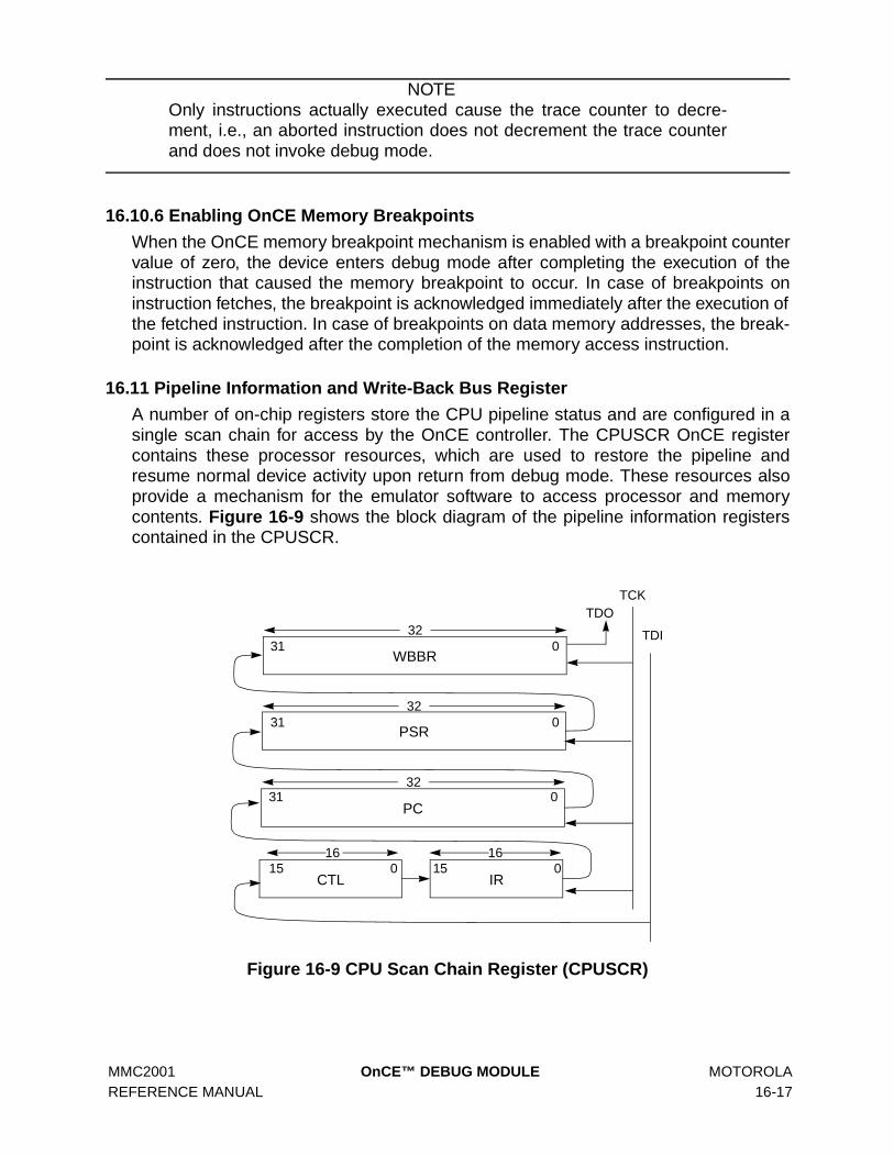
MMC2001 OnCE™ DEBUG MODULE MOTOROLA REFERENCE MANUAL 16-17
NOTEOnly instructions actually executed cause the trace counter to decre-ment, i.e., an aborted instruction does not decrement the trace counterand does not invoke debug mode.
16.10.6 Enabling OnCE Memory Breakpoints
When the OnCE memory breakpoint mechanism is enabled with a breakpoint countervalue of zero, the device enters debug mode after completing the execution of theinstruction that caused the memory breakpoint to occur. In case of breakpoints oninstruction fetches, the breakpoint is acknowledged immediately after the execution ofthe fetched instruction. In case of breakpoints on data memory addresses, the break-point is acknowledged after the completion of the memory access instruction.
16.11 Pipeline Information and Write-Back Bus Register
A number of on-chip registers store the CPU pipeline status and are configured in asingle scan chain for access by the OnCE controller. The CPUSCR OnCE registercontains these processor resources, which are used to restore the pipeline andresume normal device activity upon return from debug mode. These resources alsoprovide a mechanism for the emulator software to access processor and memorycontents. Figure 16-9 shows the block diagram of the pipeline information registerscontained in the CPUSCR.
Figure 16-9 CPU Scan Chain Register (CPUSCR)
TDO
TDI
TCK
PC
PSR
IRCTL
WBBR
32
32
32
1616
31 0
31 0
31 0
15 0 15 0
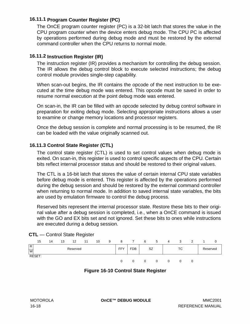
MOTOROLA OnCE™ DEBUG MODULE MMC2001 16-18 REFERENCE MANUAL
16.11.1 Program Counter Register (PC)The OnCE program counter register (PC) is a 32-bit latch that stores the value in theCPU program counter when the device enters debug mode. The CPU PC is affectedby operations performed during debug mode and must be restored by the externalcommand controller when the CPU returns to normal mode.
16.11.2 Instruction Register (IR)The instruction register (IR) provides a mechanism for controlling the debug session.The IR allows the debug control block to execute selected instructions; the debugcontrol module provides single-step capability.
When scan-out begins, the IR contains the opcode of the next instruction to be exe-cuted at the time debug mode was entered. This opcode must be saved in order toresume normal execution at the point debug mode was entered.
On scan-in, the IR can be filled with an opcode selected by debug control software inpreparation for exiting debug mode. Selecting appropriate instructions allows a userto examine or change memory locations and processor registers.
Once the debug session is complete and normal processing is to be resumed, the IRcan be loaded with the value originally scanned out.
16.11.3 Control State Register (CTL)
The control state register (CTL) is used to set control values when debug mode isexited. On scan-in, this register is used to control specific aspects of the CPU. Certainbits reflect internal processor status and should be restored to their original values.
The CTL is a 16-bit latch that stores the value of certain internal CPU state variablesbefore debug mode is entered. This register is affected by the operations performedduring the debug session and should be restored by the external command controllerwhen returning to normal mode. In addition to saved internal state variables, the bitsare used by emulation firmware to control the debug process.
Reserved bits represent the internal processor state. Restore these bits to their origi-nal value after a debug session is completed, i.e., when a OnCE command is issuedwith the GO and EX bits set and not ignored. Set these bits to ones while instructionsare executed during a debug session.
Figure 16-10 Control State Register
CTL — Control State Register 15 14 13 12 11 10 9 8 7 6 5 4 3 2 1 0
RReserved FFY FDB SZ TC Reserved
W
RESET:
0 0 0 0 0 0 0

MMC2001 OnCE™ DEBUG MODULE MOTOROLA REFERENCE MANUAL 16-19
FFY — Feed Forward Y Operand This control bit is used to force the content of the WBBR to be used as the Y operandvalue of the first instruction to be executed following an update of the CPUSCR. Thisgives the debug firmware the capability of updating processor registers by initializingthe WBBR with the desired value, setting the FFY bit, and executing a mov instruc-tion to the desired register.
FDB — Force PSR Debug Enable Mode Setting this control bit places the processor in debug enable mode. In debug enablemode, execution of the bkpt instruction as well as recognition of the BRKRQ inputcauses the processor to enter debug mode, as if the DBGRQ input had beenasserted.
SZ — Prefetch Size This control field is used to drive the CPU SIZ[1:0] outputs on the first instructionprefetch caused by issuing a OnCE command with the GO bit set and not ignored. Itshould be set to indicate a 16-bit size, i.e., 0b10. This field should be restored to itsoriginal value after a debug session is completed, i.e., when a OnCE command isissued with the GO and EX bits set and not ignored.
TC — Prefetch Transfer CodeThis control field is used to drive the CPU TC[2:0] outputs on the first instructionprefetch caused by issuing a OnCE command with the GO bit set and not ignored. Itshould typically be set to indicate a supervisor instruction access, i.e., 0b110. Thisfield should be restored to its original value after a debug session is completed, i.e.,when a OnCE command is issued with the GO and EX bits set and not ignored.
16.11.4 Write-Back Bus Register (WBBR)
The write-back bus register (WBBR) is used as a means of passing operand informa-tion between the CPU and the external command controller. Whenever the externalcommand controller needs to read the contents of a register or memory location, itforces the device to execute an instruction that brings that information to WBBR.
For example, to read the content of processor register r0, a mov r0,r0 instruction isexecuted, and the result value of the instruction is latched into the WBBR. The con-tents of WBBR can then be delivered serially to the external command controller.
To update a processor resource, this register is initialized with a data value to be writ-ten, and a mov instruction is executed which uses this value as a write-back datavalue. The FFY bit in the control state register forces the value of the WBBR to besubstituted for the normal source value of a mov instruction, thus allowing updates toprocessor registers to be performed.
16.11.5 Processor Status Register (PSR)
The OnCE processor status register (PSR) is a 32-bit latch used to read or write theM•CORE processor status register. Whenever the external command controllerneeds to save or modify the contents of the M•CORE processor status register, thisregister is used. This register is affected by the operations performed in debug modeand must be restored by the external command controller when returning to normalmode.

MOTOROLA OnCE™ DEBUG MODULE MMC2001 16-20 REFERENCE MANUAL
16.12 Instruction Address FIFO Buffer (PC FIFO)
To ease debugging activity and keep track of program flow, a first-in-first-out (FIFO)buffer stores the addresses of the last eight instruction change-of-flow prefetches thatwere issued.
The FIFO is implemented as a circular buffer containing eight 32-bit registers and one3-bit counter. All the registers have the same address, but any read access to theFIFO address causes the counter to increment and point to the next FIFO register.The registers are serially available to the external command controller through thecommon FIFO address. Figure 16-11 shows the block diagram of the PC FIFO.
Figure 16-11 OnCE PC FIFO
PC FIFO Register 0
TDOTCK
PC FIFO Register 1
PC FIFO Register 2
PC FIFO Register 3
PC FIFO Register 4
Instruction Fetch Address
CircularBufferPointer
PC FIFO Shift Register
PC FIFO Register 5
PC FIFO Register 6
PC FIFO Register 7

MMC2001 OnCE™ DEBUG MODULE MOTOROLA REFERENCE MANUAL 16-21
The FIFO is not affected by operations performed in debug mode, except for incre-menting the FIFO pointer when the FIFO is read. When debug mode is entered, theFIFO counter points to the FIFO register containing the address of the oldest of theeight change-of-flow prefetches. The first FIFO read obtains the oldest address, andthe following FIFO reads return the other addresses from the oldest to the newest (inorder of execution).
To ensure FIFO coherence, a complete set of eight reads of the FIFO must be per-formed. Each read increments the FIFO pointer, causing it to point to the next loca-tion. After eight reads, the pointer points to the same location as before the start ofthe read procedure.
16.12.1 Reserved Test Control Registers (Reserved, MEM_BIST, FTCR, LSRL)
These registers are reserved for factory testing.
WARNINGTo prevent damage to the device or system, do not access theseregisters during normal operation.
16.13 Serial Protocol Description
The following protocol permits an efficient means of communication between theOnCE external command controller and the MMC2001. Before starting any debug-ging activity, the external command controller must wait for an acknowledgment thatthe device has entered debug mode. The external command controller communicateswith the device by sending 8-bit commands to the OnCE command register and 16 to128 bits of data to one of the other OnCE registers. Both commands and data aresent or received LSB first. After sending a command, the external command control-ler must wait for the processor to acknowledge execution of certain commands beforeit can properly access another OnCE register.
16.13.1 OnCE Commands
The OnCE commands can be classified as follows:
• Read commands (the device delivers the required data)• Write commands (the device receives data and writes the data in one of the
OnCE registers)• Commands that do not have data transfers associated with them.
The commands are eight bits long and have the format shown in Figure 16-4.
16.14 Target Site Debug System Requirements
A typical debug environment consists of a target system in which the MMC2001resides in the user-defined hardware.

MOTOROLA OnCE™ DEBUG MODULE MMC2001 16-22 REFERENCE MANUAL
The external command controller acts as the medium between the MMC2001 targetsystem and a host computer. The external command controller circuit acts as a serialdebug port driver and host computer command interpreter. The controller issuescommands based on the host computer inputs from a user interface program whichcommunicates with the user.
16.15 Interface Connector For JTAG/OnCE Serial PortFigure 16-12 shows the recommended connector pinout and interface requirementsfor debug controllers that access the JTAG/OnCE port. The connector has two rowsof seven pins with 0.1 inch center-to-center spacing between pins in each row andeach column.
Figure 16-12 Recommended Connector Interface to JTAG/OnCE Port
TDI
TDO
TCLK
GPIO/SI
TARGET_RESET
KEY (No Connect)
GND
1 2
3 4
5 6
7 8
9 10
10 kΩ
10 kΩ
TOP VIEW
11 12
13 14
TARGET VDD
GPIO/SO
DBEV
(0.1 inch center-to-center)
10 kΩ
10 kΩ
TARGET VDD
TARGET VDD
TRST 10 kΩ
TMS 10 kΩ
Note: GPIO/SI and GPIO/SO are not required for OnCE operation at this time.
These pins can be used for high speed downloads with a recommended interface.
10 kΩ
Wired Or with target resetcircuit. This signal must be able to assert/monitor system reset.

MMC2001 ELECTRICAL CHARACTERISTICS MOTOROLA REFERENCE MANUAL A-1
PRELIMIN
ARYAPPENDIX A
ELECTRICAL CHARACTERISTICSThis section contains preliminary information on DC/AC electrical characteristics andAC timing specifications of the MMC2001.
A.1 Maximum Ratings
A.2 DC Electrical Specifications
Table A-1 Maximum Ratings
Rating Symbol Value Unit
Internal Supply Voltage VCCI –0.3 to + 4.5 V
External Supply Voltage VCCE –0.3 to + 4.5 V
Operating Temperature Range Ta –40 to + 85 °C
Storage Temperature TSTG –55 to + 150 °C
Table A-2 DC Electrical Specifications
Characteristic Symbol Min Max Unit
Internal Supply Voltage VCCI 1.8 3.6 V
External Supply Voltage VCCE VCCI 3.6 V
Battery Supply Voltage VCCB VCCE – 1.0 VCCE V
Input High Voltage VIH 0.7 * VCCE VCCE + 0.2 V
Input Low Voltage VIL –0.3 0.2 * VCCE V
Input Leakage Current (All Input Only Pins) IIN –10 10 µA
Hi-Z (Off State) Leakage Current (All Input, Non-Crystal Outputs, and I/O Pins)
IOZ –10 10 µA
Signal Low Input Current(TMS, TDI, TCK, TRST, DE, ROW[7:0])
IL –0.015 0.2 mA
Signal High Input Current,(TMS, TDI, TCK, TRST, DE, ROW[7:0])
IH –0.015 0.2 mA
Output High Voltage, IOH = 0.4 mA VOH 0.75 * VCCE VCCE V
Output Low Voltage, IOL = 0.8 mA VOL 0 0.18 * VCCE V
VCCB Standby Current (LVRSTIN asserted)VCCI Supply Current at 2.0 V @ 34 MHz
STOPDOZEWAIT RUN
IBATT_standby
ICC_stopICC_dozeICC_waitICC_run
—
————
3
6033
40
µA
µAmAmAmA
Pin Capacitance CIN — 10 pF
Load Capacitance CL — 50 pF
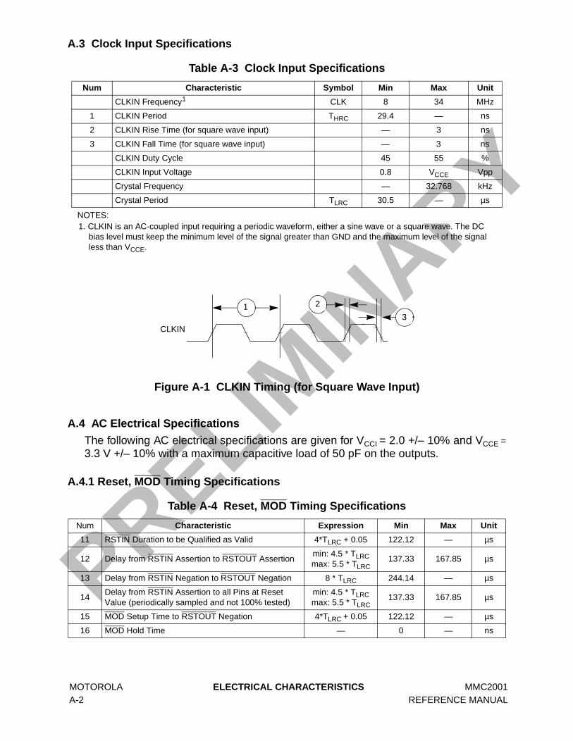
MOTOROLA ELECTRICAL CHARACTERISTICS MMC2001 A-2 REFERENCE MANUAL
PRELIMIN
ARY
A.3 Clock Input Specifications
Figure A-1 CLKIN Timing (for Square Wave Input)
A.4 AC Electrical Specifications
The following AC electrical specifications are given for VCCI = 2.0 +/– 10% and VCCE =3.3 V +/– 10% with a maximum capacitive load of 50 pF on the outputs.
A.4.1 Reset, MOD Timing Specifications
Table A-3 Clock Input Specifications
Num Characteristic Symbol Min Max Unit
CLKIN Frequency1
NOTES:1. CLKIN is an AC-coupled input requiring a periodic waveform, either a sine wave or a square wave. The DC
bias level must keep the minimum level of the signal greater than GND and the maximum level of the signal less than VCCE.
CLK 8 34 MHz
1 CLKIN Period THRC 29.4 — ns
2 CLKIN Rise Time (for square wave input) — 3 ns
3 CLKIN Fall Time (for square wave input) — 3 ns
CLKIN Duty Cycle 45 55 %
CLKIN Input Voltage 0.8 VCCE Vpp
Crystal Frequency — 32.768 kHz
Crystal Period TLRC 30.5 — µs
Table A-4 Reset, MOD Timing Specifications
Num Characteristic Expression Min Max Unit
11 RSTIN Duration to be Qualified as Valid 4*TLRC + 0.05 122.12 — µs
12 Delay from RSTIN Assertion to RSTOUT Assertionmin: 4.5 * TLRCmax: 5.5 * TLRC
137.33 167.85 µs
13 Delay from RSTIN Negation to RSTOUT Negation 8 * TLRC 244.14 — µs
14Delay from RSTIN Assertion to all Pins at Reset Value (periodically sampled and not 100% tested)
min: 4.5 * TLRCmax: 5.5 * TLRC
137.33 167.85 µs
15 MOD Setup Time to RSTOUT Negation 4*TLRC + 0.05 122.12 — µs
16 MOD Hold Time — 0 — ns
CLKIN
1 2
3

MMC2001 ELECTRICAL CHARACTERISTICS MOTOROLA REFERENCE MANUAL A-3
PRELIMIN
ARYFigure A-2 Reset Timing
Figure A-3 MOD Timing
A.4.2 External Interrupt Timing Specifications
Table A-5 External Interrupt Timing Specifications
Num Characteristic Symbol Min Max Unit
21 Minimum Edge-Triggered INTn Width High 2 * THRC+2 60.8 — ns
22 Minimum Edge-Triggered INTn Width Low 2 * THRC+2 60.8 — ns
RSTIN
All Pins
RSTOUT
11
12
14
Reset Value
13
RSTOUT
MOD
15
16

MOTOROLA ELECTRICAL CHARACTERISTICS MMC2001 A-4 REFERENCE MANUAL
PRELIMIN
ARYFigure A-4 External Interrupt Timing
A.4.3 EIM Timing Specifications
Table A-6 EIM Timing Specifications1
NOTES:1. Output timing is measured at the pin. The specifications assume a capacitive load of 50 pF.
Num Characteristic Min Max Unit
31 CLKOUT Rise to Address, R/W Valid 0 27 ns
32 CLKOUT Rise to Address, R/W Invalid (Output Hold) 0 — ns
33 CLKOUT Rise to CS Asserted 0 29 ns
34 CLKOUT Rise to CS Negated (Output Hold) 0 — ns
35CLKOUT Fall to OE, EB Asserted (Read, OEA=0),EB Asserted (Write)2
2. EB outputs are asserted for reads if the EBC bit in the corresponding CS control register is cleared.
0 16 ns
36 CLKOUT Rise to OE, EB Asserted (Read, OEA=1)2 0 16 ns
37 CLKOUT Rise to OE, EB Negated (Output Hold) (Read)2 0 — ns
37 CLKOUT Rise to EB Negated (Output Hold) (Write, WEN=0) 0 — ns
38 CLKOUT Fall to EB Negated (Output Hold) (Write, WEN=1) 0 — ns
39 CLKOUT Fall to OE, EB Asserted (WSC=0)2 0 13 ns
40 CLKOUT Rise to OE, EB Negated (Output Hold) (WSC=0)2 0 — ns
41 Data In Valid to CLKOUT rise (setup) 17 — ns
42 CLKOUT Rise to Data In Invalid (hold) 0 — ns
43 CLKOUT Rise to Data Out Valid (WSC>0) — 15 ns
44 CLKOUT Rise to Data Out Invalid (Output Hold) (WSC>0) 0 — ns
45 CLKOUT Rise to Data Out High Impedance (WSC>0) — 15 ns
46 CLKOUT Fall to Data Out Valid (WSC=0) — 17 ns
47 CLKOUT Rise to Data Out Invalid (Output Hold) (WSC=0) 0 — ns
48 CLKOUT Rise to Data Out High Impedance (WSC=0) — 17 ns
INTn
INTn
21
22

MMC2001 ELECTRICAL CHARACTERISTICS MOTOROLA REFERENCE MANUAL A-5
PRELIMIN
ARY
Figure A-5 EIM Read/Write Timing
CLKOUT
34
33
Address
41Data In(Read)
Data Out (WSC>0)(Write)
43 45
CS
OE, EB (WSC=0)
42
44
40
39
32
31
OE, EB
37
35 (OEA=0)
OE, EB (OEA=1)
37
36
EB (WEN=1)
38
35
46Data Out(Write)
47
(WSC=0)
R/W
48
EB
37
35 (WEN=0)
(Read)
(Read)
(Write)
(Write)

MOTOROLA ELECTRICAL CHARACTERISTICS MMC2001 A-6 REFERENCE MANUAL
PRELIMIN
ARY
A.4.4 ISPI Timing Specifications
Table A-7 ISPI Timing Specifications
Num Characteristic Symbol Min Max Unit
Operating Frequency (SCLK) fop(s) DC 1/8 CLK
51 Cycle Time tcyc 8 1024 CLK
52Enable Lead Time PHA=0 PHA=1
tlead 11
——
SCLK
53Enable Lag Time PHA=0 PHA=1
tlag 11
11
SCLK
54 Clock (SCLK) High Time tw(SCKH) 4 512 CLK
55 Clock (SCLK) Low Time tw(SCKL) 4 512 CLK
56 Data Setup Time (Inputs) tsu 8 — ns
57 Data Hold Time (Inputs) th 8 — ns
58 Access Time Slave ta 1 — SCLK
59 Disable Time (Hold Time) tdis — 1 SCLK
60 Data Valid (After Enable Edge) tv(s) — 5 ns
61 Data Hold Time (Output) (After Enable Edge) tho 0 — ns
62Rise Time (20% VDD to 70% VDD, CL = 20pF) Manual/Interval Mode Slave Mode
trs ——
1010
ns
63Fall Time (20% VDD to 70% VDD, CL = 20pF) Manual/Interval Mode Slave Mode
tfs 00
1010
ns
64 Sequential Transfer Delay1
NOTES:1. Signal depends on software in interval mode.
tbt 1 — SCLK
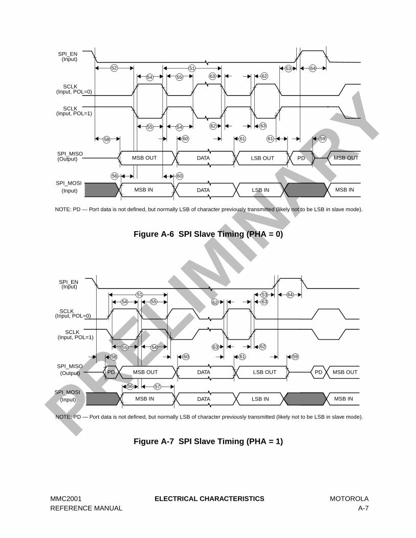
MMC2001 ELECTRICAL CHARACTERISTICS MOTOROLA REFERENCE MANUAL A-7
PRELIMIN
ARYFigure A-6 SPI Slave Timing (PHA = 0)
Figure A-7 SPI Slave Timing (PHA = 1)
SPI_EN(Input)
SCLK(Input, POL=0)
SCLK(Input, POL=1)
SPI_MISO(Output)
SPI_MOSI(Input)
MSB OUT DATA LSB OUT
MSB IN DATA LSB IN
NOTE: PD — Port data is not defined, but normally LSB of character previously transmitted (likely not to be LSB in slave mode).
5554
51
5455
62
63
63
62
53
56
60 61
MSB OUT
MSB IN
6452
61
PD
5958
60
SPI_EN(Input)
SCLK(Input, POL=0)
SCLK(Input, POL=1)
SPI_MISO(Output)
SPI_MOSI(Input)
MSB OUT DATA LSB OUT
MSB IN DATA LSB IN
NOTE: PD — Port data is not defined, but normally LSB of character previously transmitted (likely not to be LSB in slave mode).
54 55
51
55 54
63
62
62
63
53
56
60 61 59
57
MSB OUT
MSB IN
64
PD PD
58
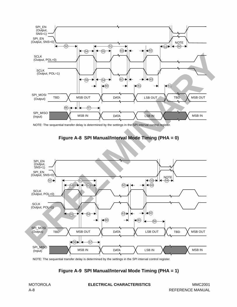
MOTOROLA ELECTRICAL CHARACTERISTICS MMC2001 A-8 REFERENCE MANUAL
PRELIMIN
ARYFigure A-8 SPI Manual/Interval Mode Timing (PHA = 0)
Figure A-9 SPI Manual/Interval Mode Timing (PHA = 1)
SPI_EN(Output,
SPI_EN(Output, SNS=0)
SCLK(Output, POL=0)
SCLK(Output, POL=1)
SPI_MOSI(Output)
SPI_MISO(Input)
MSB OUT DATA LSB OUT
MSB IN DATA LSB IN
5554
51
5455
62
63
63
53
PD*
56
60 61
57
MSB OUT
MSB IN
6452
61
TBD TBD
NOTE: The sequential transfer delay is determined by the settings in the SPI interval control register.
NOTE
62
SNS=1)
SPI_EN(Output,
SPI_EN(Output, SNS=0)
SCLK(Output, POL=0)
SCLK(Output, POL=1)
SPI_MOSI(Output)
SPI_MISO(Input)
MSB OUT DATA LSB OUTTBD
MSB IN DATA LSB IN
54 55
59
55 54
63
62
62
63
53
PD*
56
60
TBD
61
52
57
MSB OUT
MSB IN
64
NOTE: The sequential transfer delay is determined by the settings in the SPI interval control register.
NOTE51
SNS=1)
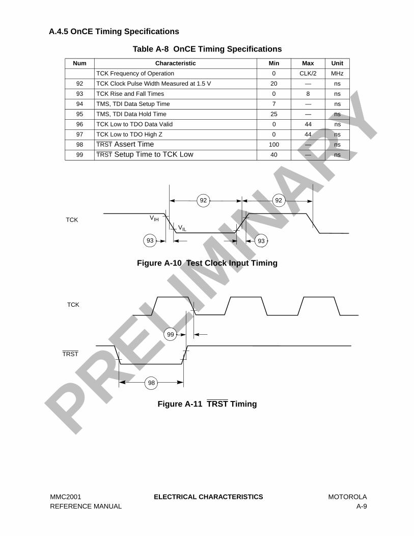
MMC2001 ELECTRICAL CHARACTERISTICS MOTOROLA REFERENCE MANUAL A-9
PRELIMIN
ARY
A.4.5 OnCE Timing Specifications
Figure A-10 Test Clock Input Timing
Figure A-11 TRST Timing
Table A-8 OnCE Timing Specifications
Num Characteristic Min Max Unit
TCK Frequency of Operation 0 CLK/2 MHz
92 TCK Clock Pulse Width Measured at 1.5 V 20 — ns
93 TCK Rise and Fall Times 0 8 ns
94 TMS, TDI Data Setup Time 7 — ns
95 TMS, TDI Data Hold Time 25 — ns
96 TCK Low to TDO Data Valid 0 44 ns
97 TCK Low to TDO High Z 0 44 ns
98 TRST Assert Time 100 — ns
99 TRST Setup Time to TCK Low 40 — ns
TCK VIH
VIL
92 92
93 93
TCK
TRST
98
99

MOTOROLA ELECTRICAL CHARACTERISTICS MMC2001 A-10 REFERENCE MANUAL
PRELIMIN
ARY
Figure A-12 Test Access Port Timing
TCK
TDI
TDO
TDO
TDO
VIH
VIL
Input Data Valid
Output Data Valid
Output Data Valid
TMS
96
94 95
97
96
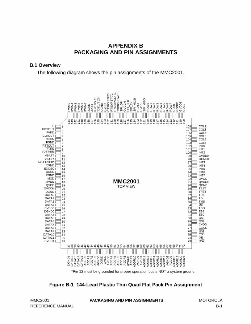
MMC2001 PACKAGING AND PIN ASSIGNMENTS MOTOROLA REFERENCE MANUAL B-1
APPENDIX B PACKAGING AND PIN ASSIGNMENTS
B.1 Overview
The following diagram shows the pin assignments of the MMC2001.
Figure B-1 144-Lead Plastic Thin Quad Flat Pack Pin Assignment
123456789101112131415161718192021222324252627282930313233343536
CS0CS1CGNDCVDDCS2CS3EB0EB1TDODETMSTDITCKTRSTTESTQGNDQVCCHQVCCINT7INT6INT5INT4INT3GGND0
COL4
GVDD0INT2INT1INT0COL7COL6COL5
COL3COL2108
107106105104103102101100
999897969594939291908988878685848382818079787776757473
109
110
111
112
113
114
115
116
117
118
119
120
121
122
123
124
125
126
127
128
129
130
131
132
133
134
135
136
137
138
139
140
141
142
143
144
727170696867666564636261605958575655545352515049484746454443424140393837
MMC2001TOP VIEW
OER/W
DATA10DATA9DATA8DATA7DATA6DATA5DATA4DGND0DVDD0DATA3DATA2DATA1DATA0QGND
QVCCHQVCCXVDDMOD
XGNDXOSC
EXOSCXGND
NOT USED*VSTBY
FVDD
VBATTLVRSTIN
RSTINRSTOUT
FGNDCLKIN
CLKOUT
GPSOUTIF
DATA11DVDD1
GG
ND
1C
OL0
RO
W7
RO
W6
RO
W5
RO
W4
RO
W3
RO
W2
RO
W1
RO
W0
SP
I_M
ISO
HV
DD
HG
ND
SP
I_M
OS
IS
PI_
EN
SP
I_C
LKQ
VC
CH
SP
I_G
PT
XD
0/P
ST
AT
0R
XD
0/P
ST
AT
1R
TS
0 /P
STA
T2
CT
S0 /
PS
TAT
3Q
VC
CQ
GN
D
PW
M3
TX
D1/
SIZ
0R
XD
1/S
IZ1
JVD
DJG
ND
PW
M0
PW
M1
PW
M2
PW
M4
PW
M5
GV
DD
1C
OL1
AD
DR
19A
DD
R18
AV
DD
2A
GN
D2
AD
DR
17A
DD
R16
AD
DR
15A
DD
R14
AD
DR
13A
DD
R12
AD
DR
11A
VD
D1
AG
ND
1A
DD
R10
AD
DR
9Q
VC
CH
AD
DR
8A
DD
R7
AD
DR
6A
DD
R5
AD
DR
4A
VD
D0
QV
CC
QG
ND
DA
TA
13
AG
ND
0A
DD
R3
AD
DR
2A
DD
R1
AD
DR
0D
AT
A15
DA
TA
14
DA
TA
12D
GN
D1
AD
DR
20A
DD
R21
*Pin 12 must be grounded for proper operation but is NOT a system ground.

MOTOROLA PACKAGING AND PIN ASSIGNMENTS MMC2001 B-2 REFERENCE MANUAL

MMC2001 PROGRAMMING REFERENCE MOTOROLA REFERENCE MANUAL C-1
APPENDIX C PROGRAMMING REFERENCE
C.1 Peripheral Module Address Assignment
The register maps of all peripheral devices for MMC2001 are located on 4096-byteboundaries. Table C-1 defines the address assignment for the on-chip components.
Table C-1 MMC2001 Address Map
Address Range (Hex) Use Access
00000000 – 0003FFFF On-Chip ROM Array Supervisor, Selective User
00040000 – 000FFFFF ROM Echoes Supervisor, Selective User
00100000 – 0FFFFFFFNot Used
(Access causes transfer error)—
10000000 – 10000FFF Interrupt Controller Supervisor Only
10001000 – 10001FFF Timer/Reset Unit Supervisor Only
10002000 – 10002FFFNot Used
(Access causes transfer error)—
10003000 – 10003FFF Keypad Port Supervisor Only
10004000 – 10004FFF External Interface Module Supervisor Only
10005000 – 10005FFF Pulse-width Modulator Supervisor Only
10006000 – 10006FFFNot Used
(Access causes transfer error)—
10007000 – 10007FFF GPIO Edge Port Supervisor Only
10008000 – 10008FFF Interval SPI Supervisor Only
10009000 – 10009FFF UART 0 Supervisor Only
1000A000 – 1000AFFF UART 1 Supervisor Only
1000B000 – 1FFFFFFFNot Used
(Access causes transfer error)—
20000000 – 2FFFFFFF External Devices Supervisor, Selective User
30000000 – 30007FFF On-Chip RAM Array Supervisor, Selective User
30008000 – 3000FFFF RAM Echoes Supervisor, Selective User
30100000 – 40000000Not Used
(Access causes transfer error)—
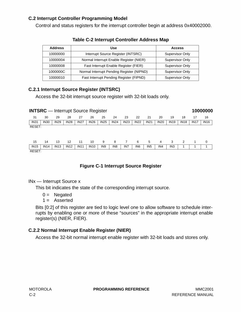
MOTOROLA PROGRAMMING REFERENCE MMC2001 C-2 REFERENCE MANUAL
C.2 Interrupt Controller Programming Model
Control and status registers for the interrupt controller begin at address 0x40002000.
C.2.1 Interrupt Source Register (INTSRC)
Access the 32-bit interrupt source register with 32-bit loads only.
Figure C-1 Interrupt Source Register
INx — Interrupt Source x This bit indicates the state of the corresponding interrupt source.
0 = Negated1 = Asserted
Bits [0:2] of this register are tied to logic level one to allow software to schedule inter-rupts by enabling one or more of these “sources” in the appropriate interrupt enableregister(s) (NIER, FIER).
C.2.2 Normal Interrupt Enable Register (NIER)
Access the 32-bit normal interrupt enable register with 32-bit loads and stores only.
Table C-2 Interrupt Controller Address Map
Address Use Access
10000000 Interrupt Source Register (INTSRC) Supervisor Only
10000004 Normal Interrupt Enable Register (NIER) Supervisor Only
10000008 Fast Interrupt Enable Register (FIER) Supervisor Only
1000000C Normal Interrupt Pending Register (NIPND) Supervisor Only
10000010 Fast Interrupt Pending Register (FIPND) Supervisor Only
INTSRC — Interrupt Source Register 1000000031 30 29 28 27 26 25 24 23 22 21 20 19 18 17 16
IN31 IN30 IN29 IN28 IN27 IN26 IN25 IN24 IN23 IN22 IN21 IN20 IN19 IN18 IN17 IN16
RESET:
15 14 13 12 11 10 9 8 7 6 5 4 3 2 1 0
IN15 IN14 IN13 IN12 IN11 IN10 IN9 IN8 IN7 IN6 IN5 IN4 IN3 1 1 1
RESET:

MMC2001 PROGRAMMING REFERENCE MOTOROLA REFERENCE MANUAL C-3
Figure C-2 Normal Interrupt Enable Register
ENx — Enable Normal Interrupt Flag xThis bit enables the corresponding interrupt source to request a normal interrupt.
0 = Disable 1 = Enable
A reset operation clears this bit.
When the enable flag is set and the corresponding interrupt line is asserted, the inter-rupt controller asserts a normal interrupt request. Enabling an interrupt source whichhas an asserted request causes that interrupt to become pending, and a request tothe CPU is asserted if not already outstanding.
C.2.3 Fast Interrupt Enable Register (FIER)
Access the 32-bit fast interrupt enable register with 32-bit loads and stores only.
Figure C-3 Fast Interrupt Enable Register
EFx — Enable Fast Interrupt Flag xThis bit enables the corresponding interrupt source to request a fast interrupt.
0 = Disable 1 = Enable
A reset operation clears this bit.
NIER — Normal Interrupt Enable Register 1000000431 30 29 28 27 26 25 24 23 22 21 20 19 18 17 16
EN31 EN30 EN29 EN28 EN27 EN26 EN25 EN24 EN23 EN22 EN21 EN20 EN19 EN18 EN17 EN16
RESET:
0 0 0 0 0 0 0 0 0 0 0 0 0 0 0 0
15 14 13 12 11 10 9 8 7 6 5 4 3 2 1 0
EN15 EN14 EN13 EN12 EN11 EN10 EN9 EN8 EN7 EN6 EN5 EN4 EN3 EN2 EN1 EN0
RESET:
0 0 0 0 0 0 0 0 0 0 0 0 0 0 0 0
FIER — Fast Interrupt Enable Register 1000000831 30 29 28 27 26 25 24 23 22 21 20 19 18 17 16
EF31 EF30 EF29 EF28 EF27 EF26 EF25 EF24 EF23 EF22 EF21 EF20 EF19 EF18 EF17 EF16
RESET:
0 0 0 0 0 0 0 0 0 0 0 0 0 0 0 0
15 14 13 12 11 10 9 8 7 6 5 4 3 2 1 0
EF15 EF14 EF13 EF12 EF11 EF10 EF9 EF8 EF7 EF6 EF5 EF4 EF3 EF2 EF1 EF0
RESET:
0 0 0 0 0 0 0 0 0 0 0 0 0 0 0 0

MOTOROLA PROGRAMMING REFERENCE MMC2001 C-4 REFERENCE MANUAL
When the enable flag is set and the corresponding interrupt line is asserted, the inter-rupt controller asserts a fast interrupt request. Enabling an interrupt source that hasan asserted request causes that interrupt to become pending, and a request to theCPU is asserted if not already outstanding.
C.2.4 Normal Interrupt Pending Register (NIPND)
Access the 32-bit normal interrupt pending register with 32-bit loads only.
Figure C-4 Normal Interrupt Pending Register
NPx — Normal Interrupt Pending Flag xThis bit indicates a pending normal interrupt request from the corresponding interruptsource.
0 = No request1 = Interrupt request pending
When a normal interrupt enable flag is set and the corresponding interrupt line isasserted, the interrupt controller asserts a normal interrupt request. The normal inter-rupt pending flags reflect the interrupt input lines which are asserted and are currentlyenabled to generate a normal interrupt.
C.2.5 Fast Interrupt Pending Register (FIPND)
Access the 32-bit read-only fast interrupt pending register with 32-bit loads only.
Figure C-5 Fast Interrupt Pending Register
NIPND — Normal Interrupt Pending Register 1000000C31 30 29 28 27 26 25 24 23 22 21 20 19 18 17 16
NP31 NP30 NP29 NP28 NP27 NP26 NP25 NP24 NP23 NP22 NP21 NP20 NP19 NP18 NP17 NP16
RESET:
0 0 0 0 0 0 0 0 0 0 0 0 0 0 0 0
15 14 13 12 11 10 9 8 7 6 5 4 3 2 1 0
NP15 NP14 NP13 NP12 NP11 NP10 NP9 NP8 NP7 NP6 NP5 NP4 NP3 NP2 NP1 NP0
RESET:
0 0 0 0 0 0 0 0 0 0 0 0 0 0 0 0
FIPND — Fast Interrupt Pending Register 1000001031 30 29 28 27 26 25 24 23 22 21 20 19 18 17 16
FP31 FP30 FP29 FP28 FP27 FP26 FP25 FP24 FP23 FP22 FP21 FP20 FP19 FP18 FP17 FP16
RESET:
0 0 0 0 0 0 0 0 0 0 0 0 0 0 0 0
15 14 13 12 11 10 9 8 7 6 5 4 3 2 1 0
FP15 FP14 FP13 FP12 FP11 FP10 FP9 FP8 FP7 FP6 FP5 FP4 FP3 FP2 FP1 FP0
RESET:
0 0 0 0 0 0 0 0 0 0 0 0 0 0 0 0

MMC2001 PROGRAMMING REFERENCE MOTOROLA REFERENCE MANUAL C-5
FPx — Fast Interrupt Pending Flag xThis bit indicates a pending fast interrupt request from the corresponding interruptsource.
0 = No request1 = Interrupt request pending
When a fast interrupt enable flag is set and the corresponding interrupt line isasserted, the interrupt controller will assert a fast interrupt request (FINT CPU input).The fast interrupt pending flags reflect the interrupt input lines which are currentlyenabled to generate a fast interrupt and are asserted.
C.3 Timer/Reset Programming Model
Table C-3 shows the timer/reset module address map.
C.3.1 Reset Source/Chip Configuration Register (RSCR)
This status and control register gives the state of the reset sources and serves tocontrol the CLKOUT pin. Writes to this register clear any previously set status bits.
Access this register with 32-bit loads and stores only.
Table C-3 Timer/Reset Module Address Map
Address Use Access
10001000 Reset Source/Chip Configuration Register (RSCR) Supervisor Only
10001004 Time-of-Day Control/Status Register (TODCSR) Supervisor Only
10001008 Time-of-Day Seconds Register (TODSR) Supervisor Only
1000100C Time-of-Day Fraction Register (TODFR) Supervisor Only
10001010 Time-of-Day Seconds Alarm Register (TODSAR) Supervisor Only
10001014 Time-of-Day Fraction Alarm Register (TODFAR) Supervisor Only
10001018 Reserved Supervisor Only
1000101C Watchdog Control Register (WCR) Supervisor Only
10001020 Watchdog Service Register (WSR) Supervisor Only
10001024 Interval Timer Control/Status Register (ITCSR) Supervisor Only
10001028 PIT Data Register (ITDR) Supervisor Only
1000102C PIT Alternate Data Register (ITADR) Supervisor Only
1000102Eto
10001FFFReserved Supervisor Only
10002000to
10002FFFNot Used (Access causes transfer error) Not Applicable

MOTOROLA PROGRAMMING REFERENCE MMC2001 C-6 REFERENCE MANUAL
* = See bit description
Figure C-6 Reset Source Register
CKOS — CLKOUT SourceThis bit controls the clock source for the CLKOUT pin. Modify this pin only when theclock output has been disabled. This bit is cleared by POR, a qualified assertion ofthe RSTIN pin, or a qualified assertion of the LVRSTIN pin.
0 = CLKOUT source is HI_REFCLK1 = CLKOUT source is LOW_REFCLK
CKOE — CLKOUT EnableThis bit controls the drive enable for the CLKOUT pin. It is cleared by POR, a qualifiedassertion of the RSTIN pin, or a qualified assertion of the LVRSTIN pin.
0 = CLKOUT is disabled and forced to the low state1 = CLKOUT is enabled and driven from the source selected by CKOS
LVRSTIN — LVRSTIN PinThis bit is set when the LVRSTIN pin is asserted to reset the MMC2001. It is notaffected by the other reset sources. When the POR bit is set, however, this bit isundefined. This bit is cleared by writing to RSCR.
RST — RSTIN PinThis bit is set when the RSTIN pin is asserted and qualified by the four-cycle qualifierto reset the MMC2001. It is not affected by the other reset sources. When the POR bitis set, however, this bit is undefined. It is cleared by writing to RSCR.
POR — Power-On ResetThis bit is set when an internal POR occurs to reset the chip. It is not affected by theother reset sources. It is cleared by writing to RSCR.
WDR — Watchdog ResetThis bit is set when the watchdog timer expires. It is cleared by POR, a qualifiedassertion of the RSTIN pin, a qualified assertion of the LVRSTIN pin, or by writing toRSCR.
RSCR — Reset Source/Chip Configuration Register 1000100031 30 29 28 27 26 25 24 23 22 21 20 19 18 17 16
R 0 0 0 0 0 0 0 0 0 0 0 0 0 0 0 0
W
RESET:
15 14 13 12 11 10 9 8 7 6 5 4 3 2 1 0
R 0 0 0 0 0 0CKOS CKOE
0 0 0 0LVRST
INRST POR WDR
W
RESET:
0* 0* * * * 0*

MMC2001 PROGRAMMING REFERENCE MOTOROLA REFERENCE MANUAL C-7
C.3.2 Time-of-Day Control/Status Register (TODCSR)
Figure C-7 TOD Control/Status Register
Access this register with 32-bit loads and stores only.
AE — Alarm EnableThis bit controls the function of the TOD alarm
0 = Alarm function is off to save power1 = Alarm function is on
AIE — Alarm Interrupt EnableThis bit controls the alarm interrupt function
0 = AIF is inhibited from reaching the CPU1 = AIF is allowed to request an interrupt
AIF — Alarm Interrupt FlagThis read-only bit is the alarm interrupt flag. It is cleared by writing to the TOD fractionalarm register (TODFAR).
0 = No alarm interrupt is present1 = Alarm interrupt is present
C.3.3 TOD Seconds Register (TODSR)
The time-of-day seconds register is a 32-bit read/write register that holds the numberof elapsed seconds. It is clocked by a 1-Hz signal generated as a carry from the TODfraction register. When TODSR is read, the content of the fraction counter is latchedinto a holding buffer to be read later. This prevents a fraction rollover between readsof the two registers from causing incorrect data to be read. When TODSR is written,the TODFR is cleared to all zeros. TODSR is not affected by the watchdog reset or bya reset initiated by the external reset signal, but is undefined after a POR.
Access this register with 32-bit loads and stores only.
TODCSR — Time-of-Day Control/Status Register 1000100431 30 29 28 27 26 25 24 23 22 21 20 19 18 17 16
R 0 0 0 0 0 0 0 0 0 0 0 0 0 0 0 0
W
RESET:
15 14 13 12 11 10 9 8 7 6 5 4 3 2 1 0
R 0 0 0 0 0 0 0 0 0 0 0 0 0AE AIE AIF
W
RESET:
0 0 0
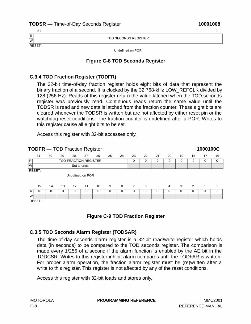
MOTOROLA PROGRAMMING REFERENCE MMC2001 C-8 REFERENCE MANUAL
Figure C-8 TOD Seconds Register
C.3.4 TOD Fraction Register (TODFR)
The 32-bit time-of-day fraction register holds eight bits of data that represent thebinary fraction of a second. It is clocked by the 32.768-kHz LOW_REFCLK divided by128 (256 Hz). Reads of this register return the value latched when the TOD secondsregister was previously read. Continuous reads return the same value until theTODSR is read and new data is latched from the fraction counter. These eight bits arecleared whenever the TODSR is written but are not affected by either reset pin or thewatchdog reset conditions. The fraction counter is undefined after a POR. Writes tothis register cause all eight bits to be set.
Access this register with 32-bit accesses only.
Figure C-9 TOD Fraction Register
C.3.5 TOD Seconds Alarm Register (TODSAR)
The time-of-day seconds alarm register is a 32-bit read/write register which holdsdata (in seconds) to be compared to the TOD seconds register. The comparison ismade every 1/256 of a second if the alarm function is enabled by the AE bit in theTODCSR. Writes to this register inhibit alarm compares until the TODFAR is written.For proper alarm operation, the fraction alarm register must be (re)written after awrite to this register. This register is not affected by any of the reset conditions.
Access this register with 32-bit loads and stores only.
TODSR — Time-of-Day Seconds Register 1000100831 0
RTOD SECONDS REGISTER
W
RESET:
Undefined on POR
TODFR — TOD Fraction Register 1000100C31 30 29 28 27 26 25 24 23 22 21 20 19 18 17 16
R TOD FRACTION REGISTER 0 0 0 0 0 0 0 0
W Set to ones
RESET:
Undefined on POR
15 14 13 12 11 10 9 8 7 6 5 4 3 2 1 0
R 0 0 0 0 0 0 0 0 0 0 0 0 0 0 0 0
W
RESET:
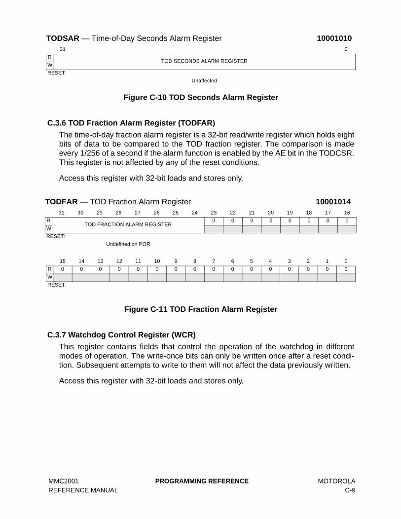
MMC2001 PROGRAMMING REFERENCE MOTOROLA REFERENCE MANUAL C-9
Figure C-10 TOD Seconds Alarm Register
C.3.6 TOD Fraction Alarm Register (TODFAR)
The time-of-day fraction alarm register is a 32-bit read/write register which holds eightbits of data to be compared to the TOD fraction register. The comparison is madeevery 1/256 of a second if the alarm function is enabled by the AE bit in the TODCSR.This register is not affected by any of the reset conditions.
Access this register with 32-bit loads and stores only.
Figure C-11 TOD Fraction Alarm Register
C.3.7 Watchdog Control Register (WCR)
This register contains fields that control the operation of the watchdog in differentmodes of operation. The write-once bits can only be written once after a reset condi-tion. Subsequent attempts to write to them will not affect the data previously written.
Access this register with 32-bit loads and stores only.
TODSAR — Time-of-Day Seconds Alarm Register 1000101031 0
RTOD SECONDS ALARM REGISTER
W
RESET:
Unaffected
TODFAR — TOD Fraction Alarm Register 1000101431 30 29 28 27 26 25 24 23 22 21 20 19 18 17 16
RTOD FRACTION ALARM REGISTER
0 0 0 0 0 0 0 0
W
RESET:
Undefined on POR
15 14 13 12 11 10 9 8 7 6 5 4 3 2 1 0
R 0 0 0 0 0 0 0 0 0 0 0 0 0 0 0 0
W
RESET:
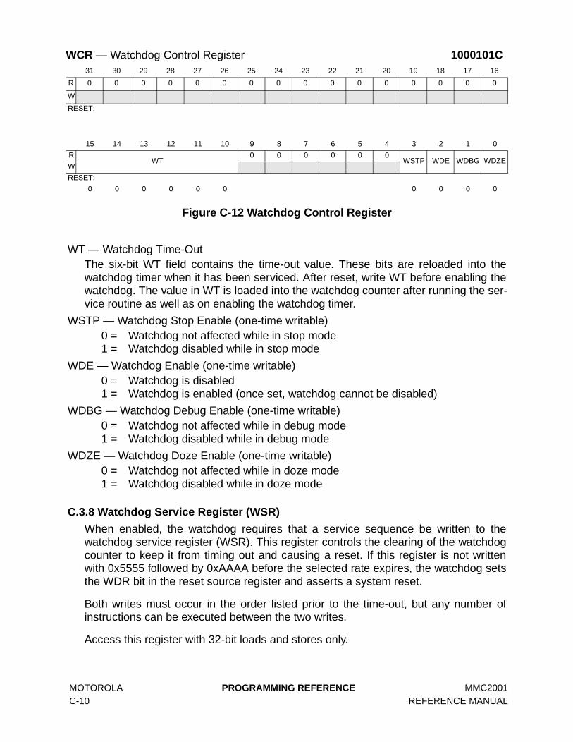
MOTOROLA PROGRAMMING REFERENCE MMC2001 C-10 REFERENCE MANUAL
Figure C-12 Watchdog Control Register
WT — Watchdog Time-Out The six-bit WT field contains the time-out value. These bits are reloaded into thewatchdog timer when it has been serviced. After reset, write WT before enabling thewatchdog. The value in WT is loaded into the watchdog counter after running the ser-vice routine as well as on enabling the watchdog timer.
WSTP — Watchdog Stop Enable (one-time writable)0 = Watchdog not affected while in stop mode1 = Watchdog disabled while in stop mode
WDE — Watchdog Enable (one-time writable)0 = Watchdog is disabled1 = Watchdog is enabled (once set, watchdog cannot be disabled)
WDBG — Watchdog Debug Enable (one-time writable)0 = Watchdog not affected while in debug mode1 = Watchdog disabled while in debug mode
WDZE — Watchdog Doze Enable (one-time writable)0 = Watchdog not affected while in doze mode1 = Watchdog disabled while in doze mode
C.3.8 Watchdog Service Register (WSR)
When enabled, the watchdog requires that a service sequence be written to thewatchdog service register (WSR). This register controls the clearing of the watchdogcounter to keep it from timing out and causing a reset. If this register is not writtenwith 0x5555 followed by 0xAAAA before the selected rate expires, the watchdog setsthe WDR bit in the reset source register and asserts a system reset.
Both writes must occur in the order listed prior to the time-out, but any number ofinstructions can be executed between the two writes.
Access this register with 32-bit loads and stores only.
WCR — Watchdog Control Register 1000101C31 30 29 28 27 26 25 24 23 22 21 20 19 18 17 16
R 0 0 0 0 0 0 0 0 0 0 0 0 0 0 0 0
W
RESET:
15 14 13 12 11 10 9 8 7 6 5 4 3 2 1 0
RWT
0 0 0 0 0 0WSTP WDE WDBG WDZE
W
RESET:
0 0 0 0 0 0 0 0 0 0

MMC2001 PROGRAMMING REFERENCE MOTOROLA REFERENCE MANUAL C-11
Figure C-13 Watchdog Service Register
C.3.9 PIT Control/Status Register (ITCSR)
Figure C-14 PIT Control and Status Register
Access this register with 32-bit loads and stores only.
STOP — Stop Mode ControlThis bit controls the function of the PIT in stop mode
0 = PIT function is not affected while in stop mode1 = PIT function is frozen while in stop mode
DOZE — Doze Mode ControlThis bit controls the function of the PIT in doze mode
0 = PIT function is not affected while in doze mode1 = PIT function is frozen while in doze mode
DBG — Debug Mode ControlThis bit controls the function of the PIT in debug mode
0 = PIT function is not affected while in debug mode1 = PIT function is frozen while in debug mode
WSR — Watchdog Service Register 1000102031 30 29 28 27 26 25 24 23 22 21 20 19 18 17 16
R 0 0 0 0 0 0 0 0 0 0 0 0 0 0 0 0
W
RESET:
15 14 13 12 11 10 9 8 7 6 5 4 3 2 1 0
R 0 0 0 0 0 0 0 0 0 0 0 0 0 0 0 0
W WATCHDOG SERVICE REGISTER
RESET:
0 0 0 0 0 0 0 0 0 0 0 0 0 0 0 0
ITCSR — Interval Timer Control and Status Register 1000102431 30 29 28 27 26 25 24 23 22 21 20 19 18 17 16
R 0 0 0 0 0 0 0 0 0 0 0 0 0 0 0 0
W
RESET:
15 14 13 12 11 10 9 8 7 6 5 4 3 2 1 0
R 0 0 0 0 0 0 0 0STOP DOZE DBG OVW ITIE ITIF RLD EN
W
RESET:
0 0 0 0 0 0 0 0

MOTOROLA PROGRAMMING REFERENCE MMC2001 C-12 REFERENCE MANUAL
OVW — Counter Overwrite EnableThis bit controls what happens to the counter value when the modulus latch is written.
0 = Modulus latch is a holding register for values to be loaded into the counterwhen the count expires to zero.
1 = Modulus latch is transparent. All writes to the latch will also overwrite thecounter contents
ITIE — PIT Interrupt EnableThis bit controls the PIT interrupt function.
0 = ITIF is inhibited from reaching the CPU1 = ITIF is allowed to request an interrupt
ITIF — PIT Interrupt FlagThis bit is the PIT interrupt flag. It is cleared by writing a one to this bit or by writing tothe PIT data register.
0 = No PIT interrupt present.1 = PIT interrupt is present.
RLD — Counter Reload ControlThis bit controls whether the value contained in the modulus latch is reloaded into thecounter when the counter reaches a count of zero or whether the counter rolls overfrom 0 to 0xFFFF.
0 = Counter rolls over to 0xFFFF.1 = Counter is reloaded from the modulus latch.
EN — PIT EnableThis bit controls the PIT enable function.
0 = PIT is disabled1 = PIT is enabled
C.3.10 PIT Data Register (ITDR)
On a write, the data becomes the new timer modulus. This value is retained and isused at the next and all subsequent reloads until changed by another write to ITDR.This value is initialized to the maximum count of 0xFFFF on reset. On a read, theITDR returns the value written in the modulus latch. The only way to directly changethe value of the count is to preload a modulus with the OVW bit set to one. Thecounter value can be read from the PIT alternate data register.
Access this register with 32-bit loads and stores only.
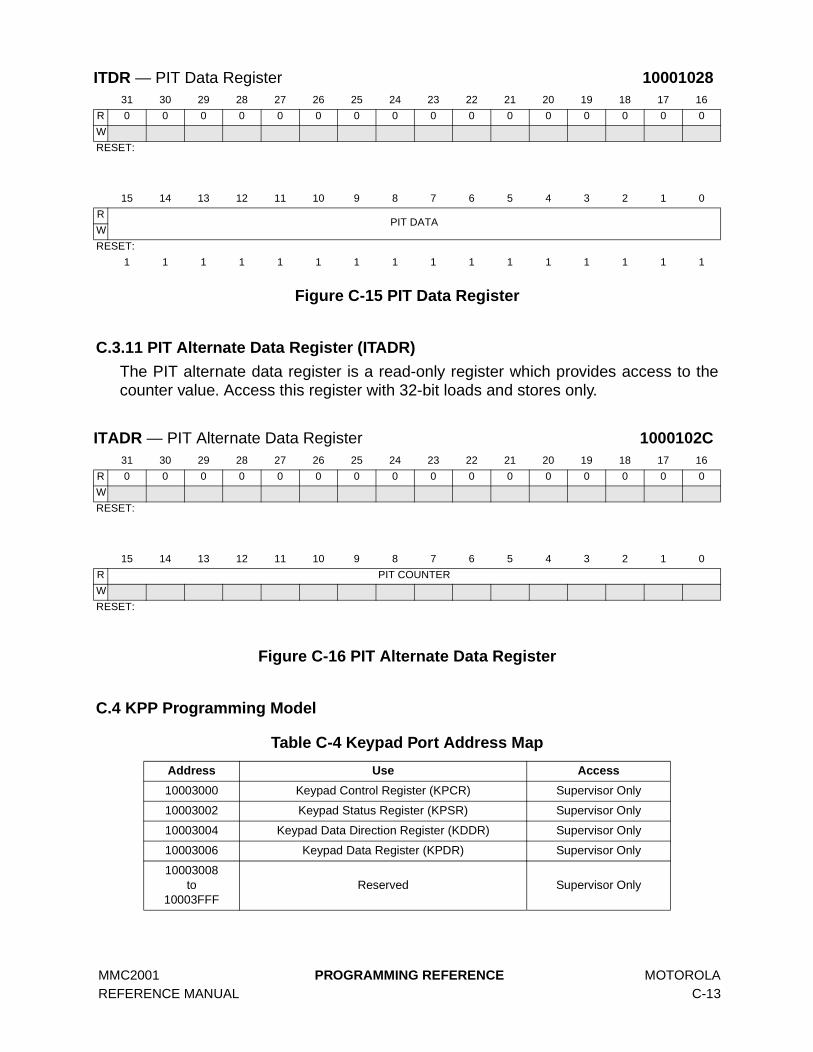
MMC2001 PROGRAMMING REFERENCE MOTOROLA REFERENCE MANUAL C-13
Figure C-15 PIT Data Register
C.3.11 PIT Alternate Data Register (ITADR)
The PIT alternate data register is a read-only register which provides access to thecounter value. Access this register with 32-bit loads and stores only.
Figure C-16 PIT Alternate Data Register
C.4 KPP Programming Model
ITDR — PIT Data Register 1000102831 30 29 28 27 26 25 24 23 22 21 20 19 18 17 16
R 0 0 0 0 0 0 0 0 0 0 0 0 0 0 0 0
W
RESET:
15 14 13 12 11 10 9 8 7 6 5 4 3 2 1 0
RPIT DATA
W
RESET:
1 1 1 1 1 1 1 1 1 1 1 1 1 1 1 1
ITADR — PIT Alternate Data Register 1000102C31 30 29 28 27 26 25 24 23 22 21 20 19 18 17 16
R 0 0 0 0 0 0 0 0 0 0 0 0 0 0 0 0
W
RESET:
15 14 13 12 11 10 9 8 7 6 5 4 3 2 1 0
R PIT COUNTER
W
RESET:
Table C-4 Keypad Port Address Map
Address Use Access
10003000 Keypad Control Register (KPCR) Supervisor Only
10003002 Keypad Status Register (KPSR) Supervisor Only
10003004 Keypad Data Direction Register (KDDR) Supervisor Only
10003006 Keypad Data Register (KPDR) Supervisor Only
10003008to
10003FFFReserved Supervisor Only

MOTOROLA PROGRAMMING REFERENCE MMC2001 C-14 REFERENCE MANUAL
C.4.1 Keypad Control Register (KPCR)
The keypad control register (KPCR) determines which of the eight possible columnstrobes are to be open drain when configured as outputs and which of the eight rowsense lines are considered in generating an interrupt to the core.
The KPCR register is byte or halfword addressable.
Figure C-17 Keypad Control Register
KCOx — Keypad Column Strobe Open-Drain Enable x0 = Column strobe output x is totem-pole drive (P-channel enabled).1 = Column strobe output x is open drain (P-channel disabled).
KREx — Keypad Row Enable x0 = Row x is not included in keypad key press detect. 1 = Row x is included in keypad key press detect.
C.4.2 Keypad Status Register (KPSR)
The keypad status register (KPSR) reflects the state of the keypress detect circuit.
The KPSR register is byte or halfword addressable.
Figure C-18 Keypad Status Register
KRIE — Key Release Interrupt Enable0 = No interrupt request is generated when KPKR is set 1 = An interrupt request is generated when KPKR is set
KDIE — Key Depress Interrupt Enable0 = No interrupt request is generated when KPKD is set 1 = An interrupt request is generated when KPKD is set
KRSS — Key Release Synchronizer SetThe key release synchronizer is set by writing a logic one into this bit. Reads return avalue of zero.
KPCR — Keypad Control Register 1000300015 14 13 12 11 10 9 8 7 6 5 4 3 2 1 0
RKCO7 KCO6 KCO5 KCO4 KCO3 KCO2 KCO1 KCO0 KRE7 KRE6 KRE5 KRE4 KRE3 KRE2 KRE1 KRE0
W
RESET:
0 0 0 0 0 0 0 0 0 0 0 0 0 0 0 0
KPSR — Keypad Status Register 1000300215 14 13 12 11 10 9 8 7 6 5 4 3 2 1 0
R 0 0 0 0 0 0KRIE KDIE
0 0 0 0 0 0KPKR KPKD
W KRSS KDSC
RESET:
0 0 0 0 0 0

MMC2001 PROGRAMMING REFERENCE MOTOROLA REFERENCE MANUAL C-15
KDSC — Key Depress Synchronizer ClearThe key depress synchronizer is cleared by writing a logic one into this bit. Readsreturn a value of zero.
KPKR — Keypad Key Release0 = No key release detected1 = All keys have been released
KPKR is cleared by writing a logic one into this bit.
KPKD — Keypad Key Depress0 = No key presses detected1 = A key has been depressed
KPKD is cleared by writing a logic one into this bit.
C.4.3 Keypad Data Direction Register (KDDR)
The bits in the keypad data direction register (KDDR) control the direction of the key-pad port pins.
The KDDR register is byte or halfword addressable.
Figure C-19 Keypad Data Direction Register
KCDDx — Keypad Column x Data Direction0 = COLx pin is configured as input. 1 = COLx pin is configured as output.
KRDDx — Keypad Row x Data Direction 0 = ROWx pin is configured as input. 1 = ROWx pin is configured as output.
C.4.4 Keypad Data Register (KPDR)
The 16-bit keypad data register is used to access the column and row data. Data writ-ten to this register is stored in an internal latch, and for each pin configured as an out-put, the stored data is driven onto the pin. A read of this register returns the value onthe pin for those bits configured as inputs. Otherwise, the value read is the valuestored in the register.
The KPDR register is byte or halfword addressable.
KDDR — Keypad Data Direction Register 1000300415 14 13 12 11 10 9 8 7 6 5 4 3 2 1 0
RKCDD7 KCDD6 KCDD5 KCDD4 KCDD3 KCDD2 KCDD1 KCDD0 KRDD7 KRDD6 KRDD5 KRDD4 KRDD3 KRDD2 KRDD1 KRDD0
W
RESET:
0 0 0 0 0 0 0 0 0 0 0 0 0 0 0 0
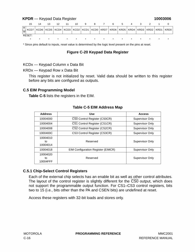
MOTOROLA PROGRAMMING REFERENCE MMC2001 C-16 REFERENCE MANUAL
* Since pins default to inputs, reset value is determined by the logic level present on the pins at reset.
Figure C-20 Keypad Data Register
KCDx — Keypad Column x Data Bit
KRDx — Keypad Row x Data Bit
This register is not initialized by reset. Valid data should be written to this registerbefore any bits are configured as outputs.
C.5 EIM Programming Model
Table C-5 lists the registers in the EIM.
C.5.1 Chip-Select Control Registers
Each of the external chip selects has an enable bit as well as other control attributes.The layout of the control register is slightly different for the CS0 output, which doesnot support the programmable output function. For CS1–CS3 control registers, bitstwo to 15 (i.e., bits other than the PA and CSEN bits) are undefined at reset.
Access these registers with 32-bit loads and stores only.
KPDR — Keypad Data Register 1000300615 14 13 12 11 10 9 8 7 6 5 4 3 2 1 0
RKCD7 KCD6 KCD5 KCD4 KCD3 KCD2 KCD1 KCD0 KRD7 KRD6 KRD5 KRD4 KRD3 KRD2 KRD1 KRD0
W
RESET:
* * * * * * * * * * * * * * * *
Table C-5 EIM Address Map
Address Use Access
10004000 CS0 Control Register (CS0CR) Supervisor Only
10004004 CS1 Control Register (CS1CR) Supervisor Only
10004008 CS2 Control Register (CS2CR) Supervisor Only
1000400C CS3 Control Register (CS3CR) Supervisor Only
10004010to
10004014Reserved Supervisor Only
10004018 EIM Configuration Register (EIMCR) Supervisor Only
10004020to
10004FFFReserved Supervisor Only
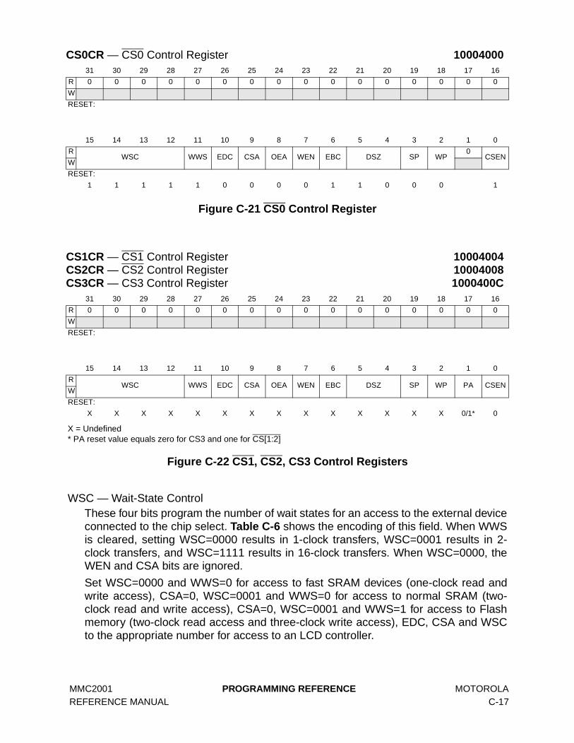
MMC2001 PROGRAMMING REFERENCE MOTOROLA REFERENCE MANUAL C-17
Figure C-21 CS0 Control Register
X = Undefined* PA reset value equals zero for CS3 and one for CS[1:2]
Figure C-22 CS1, CS2, CS3 Control Registers
WSC — Wait-State ControlThese four bits program the number of wait states for an access to the external deviceconnected to the chip select. Table C-6 shows the encoding of this field. When WWSis cleared, setting WSC=0000 results in 1-clock transfers, WSC=0001 results in 2-clock transfers, and WSC=1111 results in 16-clock transfers. When WSC=0000, theWEN and CSA bits are ignored.
Set WSC=0000 and WWS=0 for access to fast SRAM devices (one-clock read andwrite access), CSA=0, WSC=0001 and WWS=0 for access to normal SRAM (two-clock read and write access), CSA=0, WSC=0001 and WWS=1 for access to Flashmemory (two-clock read access and three-clock write access), EDC, CSA and WSCto the appropriate number for access to an LCD controller.
CS0CR — CS0 Control Register 1000400031 30 29 28 27 26 25 24 23 22 21 20 19 18 17 16
R 0 0 0 0 0 0 0 0 0 0 0 0 0 0 0 0
W
RESET:
15 14 13 12 11 10 9 8 7 6 5 4 3 2 1 0
RWSC WWS EDC CSA OEA WEN EBC DSZ SP WP
0CSEN
W
RESET:
1 1 1 1 1 0 0 0 0 1 1 0 0 0 1
CS1CR — CS1 Control Register 10004004CS2CR — CS2 Control Register 10004008CS3CR — CS3 Control Register 1000400C
31 30 29 28 27 26 25 24 23 22 21 20 19 18 17 16
R 0 0 0 0 0 0 0 0 0 0 0 0 0 0 0 0
W
RESET:
15 14 13 12 11 10 9 8 7 6 5 4 3 2 1 0
RWSC WWS EDC CSA OEA WEN EBC DSZ SP WP PA CSEN
W
RESET:
X X X X X X X X X X X X X X 0/1* 0

MOTOROLA PROGRAMMING REFERENCE MMC2001 C-18 REFERENCE MANUAL
WWS — Write Wait StateThis bit is used to determine if an additional wait state is required for write cycles.This is useful for writing to Flash memories that require additional data setup time.
0 = Reads and writes are the same length.1 = An additional wait state is inserted for write cycles unless WSC is set to
1111. Setting WSC to 1111 results in 16-clock transfers regardless of theWWS bit. Read cycles are not affected.
EDC — Extra Dead CycleThis bit is used to determine if an idle cycle is inserted after a read cycle for back-to-back external transfers to eliminate data bus contention. This is useful for slow mem-ory and peripherals.
0 = Back-to-back external transfers occur normally, i.e., no idle cycle is insertedafter a read cycle.
1 = An idle cycle is inserted after a read cycle for back-to-back externaltransfers, unless the next cycle is a read cycle to the same CS bank.
CSA — Chip Select AssertThis bit is used for devices that require additional address setup time and additionaladdress/data hold times. It determines when the chip select is asserted and whetheran idle cycle is inserted between back-to-back external transfers. If WSC=0000, thisbit is ignored.
0 = Chip select is asserted normally, i.e., as early as possible. No idle cycle isinserted between back-to-back external transfers.
1 = Chip select is asserted a clock later during both read and write cycles. Inaddition, an idle cycle is inserted between back-to-back external transfers.
Table C-6 Wait State Control Field Settings
Number of Wait States
WSC[3:0] WWS = 0 WWS = 1
Read Access Write Access Read Access Write Access
0000 0 0 0 1
0001 1 1 1 2
0010 2 2 2 3
0011 3 3 3 4
0100 4 4 4 5
0101 5 5 5 6
0110 6 6 6 7
0111 7 7 7 8
1000 8 8 8 9
1001 9 9 9 10
1010 10 10 10 11
1011 11 11 11 12
1100 12 12 12 13
1101 13 13 13 14
1110 14 14 14 15
1111 15 15 15 15

MMC2001 PROGRAMMING REFERENCE MOTOROLA REFERENCE MANUAL C-19
OEA — OE AssertThis bit is used to determine when OE is asserted during a read cycle. If WSC=0000,this bit is ignored and OE is asserted for one half of a clock cycle only. If EBC in thecorresponding register is cleared, then the EB[0:1] outputs are similarly affected.
0 = OE is asserted normally, i.e., as early as possible.1 = OE is asserted one half of a clock cycle later during a read cycle to this chip
select address space. The cycle length and write cycles are not affected.
WEN — EB NegateThis bit is used to determine when EB[0:1] outputs are negated during a write cycle.This is useful to meet data hold time requirements for slow memories. If WSC=0000,this bit is ignored and EB[0:1] outputs are asserted for one half of a clock cycle only.
0 = EB[0:1] are negated normally, i.e., as late as possible.1 = EB[0:1] are negated one half of a clock cycle earlier during a write cycle to
this chip select address space. The cycle length and read cycles are notaffected.
EBC — Enable Byte Control This bit is used to indicate which access types should assert the enable byte outputs(EB[0:1]).
0 = Read and write accesses are both allowed to assert the EB[0:1] outputs,thus configuring them as byte enables.
1 = Only write accesses are allowed to assert the EB[0:1] outputs, thusconfiguring them as byte write enables. The EB[0:1] outputs should beconfigured as byte write enables for accesses to dual x8 memories.
DSZ — Data Port SizeThis field defines the width of the device data port.
SP — Supervisor ProtectThis bit is used to restrict accesses to the address range defined by the correspond-ing chip select if the access is attempted in the user mode of CPU operation.
0 = User mode accesses are allowed in this chip select address range1 = User mode accesses are prohibited. An attempted access to an address
mapped by this chip select in user mode will result in a TEA to the CPU andno assertion of the chip select output.
Table C-7 Data Port Size Field Settings
Value Meaning
00 8-bit port, resides on DATA[15:8] pins
01 8-bit port, resides on DATA[7:0] pins
10 16-bit port
11 Reserved

MOTOROLA PROGRAMMING REFERENCE MMC2001 C-20 REFERENCE MANUAL
WP — Write ProtectThis bit is used to restrict writes to the address range defined by the correspondingchip select.
0 = Writes are allowed in this chip select address space.1 = Writes are prohibited. An attempt to write to an address mapped by this chip
select will result in a TEA to the CPU and no assertion of the chip selectoutput.
PA — Pin AssertThis bit is used to control the chip select pin when it is operating as a programmableoutput pin (i.e. the CSEN bit clear). This bit is ignored if the CSEN bit is set. At reset,PA bit is set for CS[1:2] and cleared for CS3.
0 = Brings chip select output to logic-low level1 = Brings chip select output to logic-high level
CSEN — Chip Select EnableThis bit controls the operation of the chip select pin.
0 = Chip select function is disabled. An attempted access to an address mappedby this chip select will result in TEA assertion to the CPU and no assertion ofthe chip select output.
When disabled, the pin is a general-purpose output controlled by thevalue of the PA control bit. When CSEN0 is clear, CS0 is inactive.
1 = Chip select is enabled and is asserted when an access address falls withinthe range specified in Table C-8. With the exception of CS0, this bit iscleared by reset, disabling the chip select output pin.
CSEN0 is set at reset to allow CS0 to select from an external boot ROM if MOD isdriven to a logic-low level four LOW_REFCLK clock cycles before RSTOUT negation.
When the chip select is enabled, the PA control bit is ignored.
C.5.2 EIM Configuration Register
The EIM configuration register contains control bits that configure the EIM and otherinternal blocks for certain operation modes.
Access this register with 32-bit loads and stores only.
Table C-8 Chip-Select Address Range
ADDR[31:24] Chip Select
— Inactive
00101101 CS0
00101111 CS1
00101110 CS2
00101100 CS3
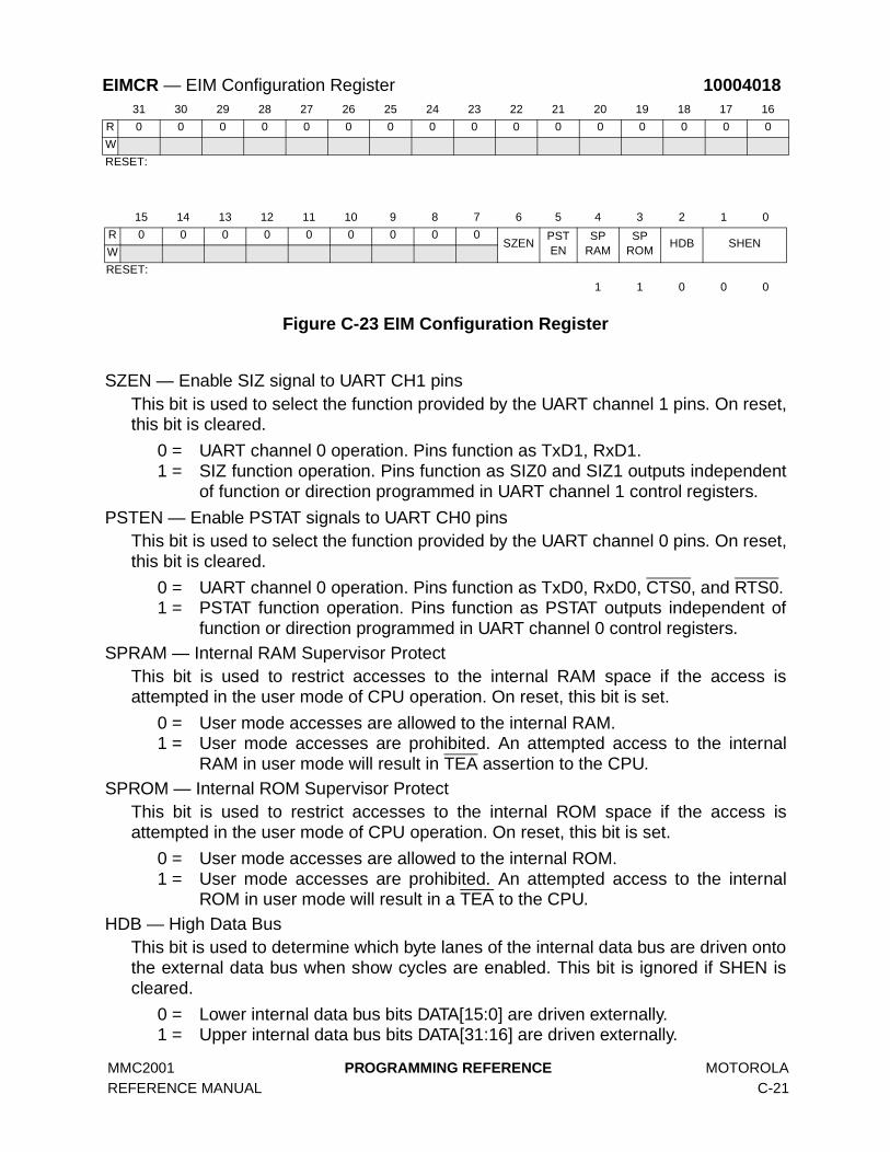
MMC2001 PROGRAMMING REFERENCE MOTOROLA REFERENCE MANUAL C-21
Figure C-23 EIM Configuration Register
SZEN — Enable SIZ signal to UART CH1 pinsThis bit is used to select the function provided by the UART channel 1 pins. On reset,this bit is cleared.
0 = UART channel 0 operation. Pins function as TxD1, RxD1.1 = SIZ function operation. Pins function as SIZ0 and SIZ1 outputs independent
of function or direction programmed in UART channel 1 control registers.
PSTEN — Enable PSTAT signals to UART CH0 pinsThis bit is used to select the function provided by the UART channel 0 pins. On reset,this bit is cleared.
0 = UART channel 0 operation. Pins function as TxD0, RxD0, CTS0, and RTS0.1 = PSTAT function operation. Pins function as PSTAT outputs independent of
function or direction programmed in UART channel 0 control registers.SPRAM — Internal RAM Supervisor Protect
This bit is used to restrict accesses to the internal RAM space if the access isattempted in the user mode of CPU operation. On reset, this bit is set.
0 = User mode accesses are allowed to the internal RAM.1 = User mode accesses are prohibited. An attempted access to the internal
RAM in user mode will result in TEA assertion to the CPU. SPROM — Internal ROM Supervisor Protect
This bit is used to restrict accesses to the internal ROM space if the access isattempted in the user mode of CPU operation. On reset, this bit is set.
0 = User mode accesses are allowed to the internal ROM.1 = User mode accesses are prohibited. An attempted access to the internal
ROM in user mode will result in a TEA to the CPU. HDB — High Data Bus
This bit is used to determine which byte lanes of the internal data bus are driven ontothe external data bus when show cycles are enabled. This bit is ignored if SHEN iscleared.
0 = Lower internal data bus bits DATA[15:0] are driven externally.1 = Upper internal data bus bits DATA[31:16] are driven externally.
EIMCR — EIM Configuration Register 1000401831 30 29 28 27 26 25 24 23 22 21 20 19 18 17 16
R 0 0 0 0 0 0 0 0 0 0 0 0 0 0 0 0
W
RESET:
15 14 13 12 11 10 9 8 7 6 5 4 3 2 1 0
R 0 0 0 0 0 0 0 0 0SZEN
PSTEN
SPRAM
SPROM
HDB SHENW
RESET:
1 1 0 0 0
MOTOROLA PROGRAMMING REFERENCE MMC2001 C-22 REFERENCE MANUAL
SHEN — Show Cycle EnableThese two bits are used to determine what the EIM does with the external bus duringinternal transfers (i.e., an access to the internal ROM, RAM or peripherals). Whenshow cycles are enabled, the internal address and data bus are driven externally. Onreset, show cycles are disabled.
C.6 PWM Module
This section describes the registers and control bits in the PWM module. All registersreset to 0x0000.
These registers must be accessed with halfword accesses. Accesses other than half-word in size result in undefined activity.
Table C-9 Show Cycle Enable Field Settings
Value Meaning
00Show cycles disabled. The external address bus is driven with the last valid external address, and the data bus values are held by bus keepers.
01Show cycles enabled. Internal termination to the CPU during idle cycles caused by EDC or CSA being set follows normal operation. This means that internal transfers that occur during EDC/CSA idle cycles will not be visible externally.
10Show cycles enabled. Internal termination to the CPU during idle cycles caused by EDC or CSA being set is delayed by one clock. This ensures that all internal transfers can be externally monitored, at the expense of performance.
11 Reserved
Table C-10 PWM Address Map
Address Use Access
10005000 PWM0 Control Register (PWMCR0) Supervisor Only
10005002 PWM0 Period Register (PWMPR0) Supervisor Only
10005004 PWM0 Width Register (PWMWR0) Supervisor Only
10005006 PWM0 Counter Register (PWMCTR0) Supervisor Only
10005008 PWM1 Control Register (PWMCR1) Supervisor Only
1000500A PWM1 Period Register (PWMPR1) Supervisor Only
1000500C PWM1 Width Register (PWMWR1) Supervisor Only
1000500E PWM1 Counter Register (PWMCTR1) Supervisor Only
10005010 PWM2 Control Register (PWMCR2) Supervisor Only
10005012 PWM2 Period Register (PWMPR2) Supervisor Only
10005014 PWM2 Width Register (PWMWR2) Supervisor Only
10005016 PWM2 Counter Register (PWMCTR2) Supervisor Only
10005018 PWM3 Control Register (PWMCR3) Supervisor Only
1000501A PWM3 Period Register (PWMPR3) Supervisor Only
1000501C PWM3 Width Register (PWMWR3) Supervisor Only
1000501E PWM3 Counter Register (PWMCTR3) Supervisor Only
10005020 PWM4 Control Register (PWMCR4) Supervisor Only
10005022 PWM4 Period Register (PWMPR4) Supervisor Only
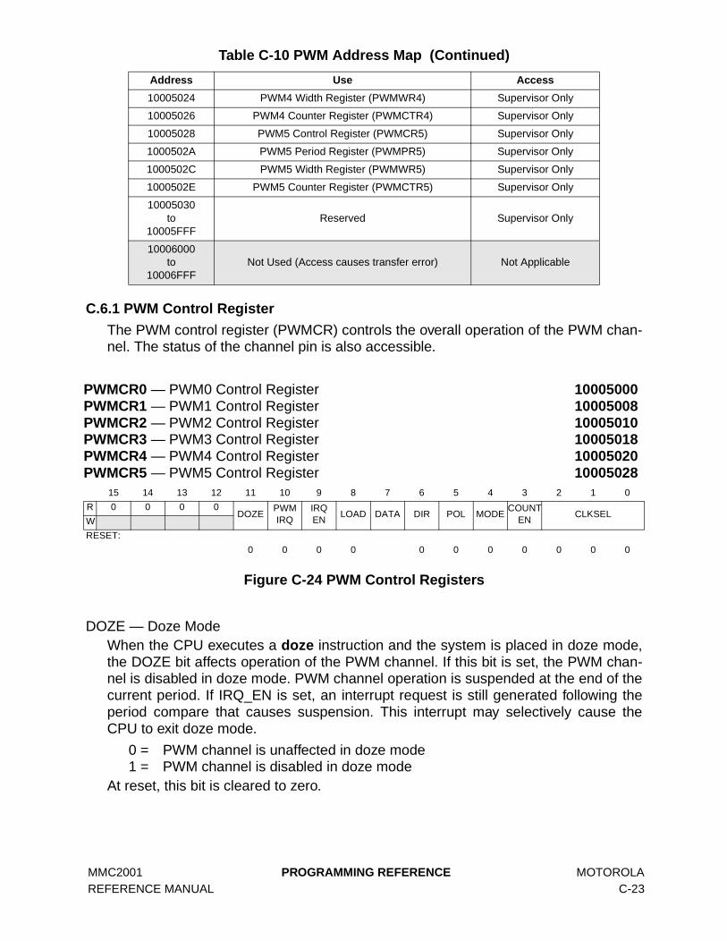
MMC2001 PROGRAMMING REFERENCE MOTOROLA REFERENCE MANUAL C-23
C.6.1 PWM Control Register
The PWM control register (PWMCR) controls the overall operation of the PWM chan-nel. The status of the channel pin is also accessible.
Figure C-24 PWM Control Registers
DOZE — Doze ModeWhen the CPU executes a doze instruction and the system is placed in doze mode,the DOZE bit affects operation of the PWM channel. If this bit is set, the PWM chan-nel is disabled in doze mode. PWM channel operation is suspended at the end of thecurrent period. If IRQ_EN is set, an interrupt request is still generated following theperiod compare that causes suspension. This interrupt may selectively cause theCPU to exit doze mode.
0 = PWM channel is unaffected in doze mode1 = PWM channel is disabled in doze mode
At reset, this bit is cleared to zero.
10005024 PWM4 Width Register (PWMWR4) Supervisor Only
10005026 PWM4 Counter Register (PWMCTR4) Supervisor Only
10005028 PWM5 Control Register (PWMCR5) Supervisor Only
1000502A PWM5 Period Register (PWMPR5) Supervisor Only
1000502C PWM5 Width Register (PWMWR5) Supervisor Only
1000502E PWM5 Counter Register (PWMCTR5) Supervisor Only
10005030to
10005FFFReserved Supervisor Only
10006000to
10006FFFNot Used (Access causes transfer error) Not Applicable
PWMCR0 — PWM0 Control Register 10005000PWMCR1 — PWM1 Control Register 10005008PWMCR2 — PWM2 Control Register 10005010PWMCR3 — PWM3 Control Register 10005018PWMCR4 — PWM4 Control Register 10005020PWMCR5 — PWM5 Control Register 10005028
15 14 13 12 11 10 9 8 7 6 5 4 3 2 1 0
R 0 0 0 0DOZE
PWMIRQ
IRQEN
LOAD DATA DIR POL MODECOUNT
ENCLKSEL
W
RESET:
0 0 0 0 0 0 0 0 0 0 0
Table C-10 PWM Address Map (Continued)
Address Use Access

MOTOROLA PROGRAMMING REFERENCE MMC2001 C-24 REFERENCE MANUAL
PWM IRQ — PWM Interrupt RequestThis bit indicates that an interrupt was posted by a period compare. This bit can beset by the user to post a PWM interrupt immediately for debugging purposes. This bitis cleared automatically after it is read while set. If IRQ EN is cleared, this bit remainscleared.
0 = No interrupt posted1 = PWM period rolled over
IRQ EN — Interrupt Request EnableThis bit controls PWM interrupt generation. While this bit is low, the interrupt is dis-abled.
0 = PWM interrupt disabled1 = PWM interrupt enabled
LOAD — Load PWMPR and PWMWRSetting this bit forces a new period. The period and width registers are loaded into thecomparator latches and the counter is reset. This bit is cleared automatically after theload has been performed. The actual load occurs some time after the CPU writes thisbit, as the load occurs on the next rising PCLK edge following internal synchroniza-tion. Forcing a load of the comparator latches and counter in this manner must bedone with caution to avoid unexpected pin behavior.
DATA — PWM DataThis bit indicates or controls the current state of the PWM pin. When the pin is config-ured as a general-purpose output, the logical value written to this bit is used to drivethe pin. When the pin is configured as a general-purpose input, the pin value isreflected by this bit. When the pin is configured in PWM mode, the bit reflects thevalue being driven on the pin by the PWM logic.
DIR — DirectionThis bit controls the direction of the pin when used as a GPIO pin. This bit has noaffect when MODE indicates PWM mode.
0 = Pin is an input pin1 = Pin is an output pin
POL — PolarityThis bit controls the polarity of the pin when used as a PWM output pin. Normally, theoutput pin is set high at period boundaries and goes low when a width compare eventoccurs.
This bit is ignored if the pin is being used as a GPIO pin.0 = Normal PWM polarity1 = Inverted PWM polarity
MODE — PWM ModeThis bit selects whether the PWM pin is used for GPIO or for the PWM function.
0 = General-purpose I/O mode1 = PWM mode

MMC2001 PROGRAMMING REFERENCE MOTOROLA REFERENCE MANUAL C-25
COUNT EN — Counter EnableThis bit enables or disables the PWM counter. The counter is actually enabled or dis-abled some time after the CPU writes this bit, as the enable occurs on the next risingPCLK edge following internal synchronization. Disabling the counter once it has beenrunning occurs following the next period match.
0 = PWM disabled. While disabled, the counter is in low-power mode and doesnot count. The following events occur:When the output pin is configured to operate in PWM mode (MODE =1), theoutput pin is forced to the setting of the POL bit.The counter is reset to 00 and frozen.
The contents of the width and period registers are loaded into the compara-tors.The comparators are disabled.If the counter has been running, and the actual disable occurs at the occur-rence of a period match, an interrupt request may still be generated, eventhough the counter is being disabled. To avoid this, write the interrupt enablecontrol bit (IRQ_EN) to zero when disabling the counter.
1 = PWM is enabled and begins a new period. The following events occur:The output pin changes state to start a new period (if width != 0 andperiod != 0 and width < period).The counter is released and begins countingThe comparators are enabledThe PWM IRQ bit is set, indicating the start of a new period if IRQ EN is set.
CLK SEL — Clock SelectThese bits select the output of the divider chain.
C.6.2 PWM Period Register
The PWM period register (PWMPR) controls the period of the PWM by defining thenumber of PCLKs in the period. When the counter value matches the value in thisregister, an interrupt is posted and the counter is reset to start another period.
Table C-11 Clock Select Field Values
Value Divide By
000 4
001 8
010 16
011 64
100 256
101 2048
110 16384
111 65536

MOTOROLA PROGRAMMING REFERENCE MMC2001 C-26 REFERENCE MANUAL
Figure C-25 PWM Period Registers
PERIOD — Pulse PeriodThis value causes the counter to be reset. There is one special case. When PERIOD= 0, the output is never set high (0% duty cycle). In this case, the comparator isloaded and the counter is reset on every PCLK. In addition, if enabled, an interruptrequest is generated on every PCLK.
C.6.3 PWM Width Register
The PWM width register (PWMWR) defines the pulse width in PCLKs. When thecounter matches the value in this register, the output is reset for the duration of theperiod. Note that if the value in this register is not less than the period register, theoutput will never be reset, resulting in a 100% duty cycle.
Figure C-26 PWM Width Registers
WIDTH — Pulse WidthWhen the counter reaches the value in this register, the output is reset.
PWMPR0 — PWM0 Period Register 10005002PWMPR1 — PWM1 Period Register 1000500APWMPR2 — PWM2 Period Register 10005012PWMPR3 — PWM3 Period Register 1000501APWMPR4 — PWM4 Period Register 10005022PWMPR5 — PWM5 Period Register 1000502A
15 14 13 12 11 10 9 8 7 6 5 4 3 2 1 0
R 0 0 0 0 0 0PERIOD
W
RESET:
0 0 0 0 0 0 0 0 0 0
PWMWR0 — PWM0 Width Register 10005004PWMWR1 — PWM1 Width Register 1000500CPWMWR2 — PWM2 Width Register 10005014PWMWR3 — PWM3 Width Register 1000501CPWMWR4 — PWM4 Width Register 10005024PWMWR5 — PWM5 Width Register 1000502C
15 14 13 12 11 10 9 8 7 6 5 4 3 2 1 0
R 0 0 0 0 0 0WIDTH
W
RESET:
0 0 0 0 0 0 0 0 0 0

MMC2001 PROGRAMMING REFERENCE MOTOROLA REFERENCE MANUAL C-27
C.6.4 PWM Counter Register
The read-only PWM counter register (PWMCR) holds the current count value. It canbe read at any time without disturbing the counter.
Figure C-27 PWM Count Registers
COUNT — Count ValueThis is the current count value.
C.7 Edge Port Programming Model
Access the edge port registers with halfword accesses.
C.7.1 Edge Port Pin Assignment Register (EPPAR)
The 16-bit read/write edge port pin assignment register (EPPAR) configures each ofthe interrupt pins as either level-sensitive or edge-sensitive. Rising, falling, or bothedges can be selected as the active edge. Requests are always generated out of thisblock but may be masked within the interrupt controller module. The functionality ofthis register is independent of the programmed pin direction.
PWMCR0 — PWM0 Counter Register 10005006PWMCR1 — PWM1 Counter Register 1000500EPWMCR2 — PWM2 Counter Register 10005016PWMCR3 — PWM3 Counter Register 1000501EPWMCR4 — PWM4 Counter Register 10005026PWMCR5 — PWM5 Counter Register 1000502E
15 14 13 12 11 10 9 8 7 6 5 4 3 2 1 0
R 0 0 0 0 0 0COUNT
W
RESET:
0 0 0 0 0 0 0 0 0 0
Table C-12 GPIO Edge Port Address Map
Address Use Access
10007000 Edge Port Pin Assignment Register (EPPAR) Supervisor Only
10007002 Edge Port Data Direction Register (EPDDR) Supervisor Only
10007004 Edge Port Data Register (EPDR) Supervisor Only
10007006 Edge Port Flag Register (EPFR) Supervisor Only
10007008to
10007FFFReserved Supervisor Only
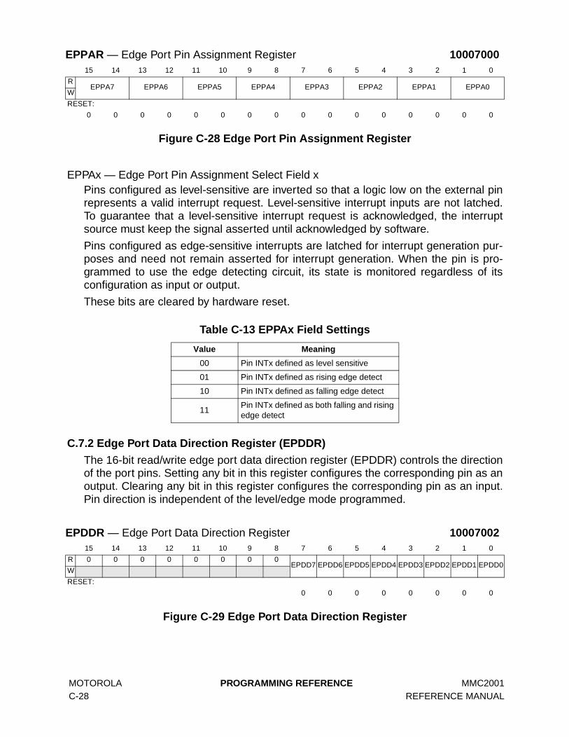
MOTOROLA PROGRAMMING REFERENCE MMC2001 C-28 REFERENCE MANUAL
Figure C-28 Edge Port Pin Assignment Register
EPPAx — Edge Port Pin Assignment Select Field x Pins configured as level-sensitive are inverted so that a logic low on the external pinrepresents a valid interrupt request. Level-sensitive interrupt inputs are not latched.To guarantee that a level-sensitive interrupt request is acknowledged, the interruptsource must keep the signal asserted until acknowledged by software.
Pins configured as edge-sensitive interrupts are latched for interrupt generation pur-poses and need not remain asserted for interrupt generation. When the pin is pro-grammed to use the edge detecting circuit, its state is monitored regardless of itsconfiguration as input or output.
These bits are cleared by hardware reset.
C.7.2 Edge Port Data Direction Register (EPDDR)
The 16-bit read/write edge port data direction register (EPDDR) controls the directionof the port pins. Setting any bit in this register configures the corresponding pin as anoutput. Clearing any bit in this register configures the corresponding pin as an input.Pin direction is independent of the level/edge mode programmed.
Figure C-29 Edge Port Data Direction Register
EPPAR — Edge Port Pin Assignment Register 1000700015 14 13 12 11 10 9 8 7 6 5 4 3 2 1 0
REPPA7 EPPA6 EPPA5 EPPA4 EPPA3 EPPA2 EPPA1 EPPA0
W
RESET:
0 0 0 0 0 0 0 0 0 0 0 0 0 0 0 0
Table C-13 EPPAx Field Settings
Value Meaning
00 Pin INTx defined as level sensitive
01 Pin INTx defined as rising edge detect
10 Pin INTx defined as falling edge detect
11Pin INTx defined as both falling and rising edge detect
EPDDR — Edge Port Data Direction Register 1000700215 14 13 12 11 10 9 8 7 6 5 4 3 2 1 0
R 0 0 0 0 0 0 0 0EPDD7 EPDD6 EPDD5 EPDD4 EPDD3 EPDD2 EPDD1 EPDD0
W
RESET:
0 0 0 0 0 0 0 0

MMC2001 PROGRAMMING REFERENCE MOTOROLA REFERENCE MANUAL C-29
EPDDx — Edge Port Data Direction x0 = Pin INTx is an input.1 = Pin INTx is an output.
These bits are cleared by reset.
C.7.3 Edge Port Data Register (EPDR)
The edge port data register (EPDR) is a 16-bit register. Writes to EPDR are stored inan internal latch, and if any pin of the port is configured as an output, the data storedfor that bit is driven onto the pin. Reads of this register return the value sensed on thepins for those pins configured as inputs, or the data stored in the register for the pinsconfigured as outputs.
X = Unaffected by reset
Figure C-30 Edge Port Data Register
EPD[7:0] — Edge Port Data Bits 7:0See the above description. These bits are not affected by hardware reset.
C.7.4 Edge Port Flag Register (EPFR)
The 16-bit read/write edge port flag register (EPFR) indicates whether the selectededge has been detected on the port pins.
Figure C-31 Edge Port Flag Register
EPFx — Edge Port Flag Bit x0 = Selected edge for INTx pin has not been detected.1 = Selected edge for INTx pin has been detected.
Bits in this register are set when the programmed edge is detected on the corre-sponding pin. A bit remains set until cleared by writing it to a one. Pin transitions donot affect this register if the pin is configured as level sensitive (EPPARn=00), and thecorresponding flag bit(s) are cleared to zero in this case. When a pin is configured asa general-purpose output, writes to EPDR which cause the selected level or edge
EPDR — Edge Port Data Register 1000700415 14 13 12 11 10 9 8 7 6 5 4 3 2 1 0
R 0 0 0 0 0 0 0 0EPD7 EPD6 EPD5 EPD4 EPD3 EPD2 EPD1 EPD0
W
RESET:
X X X X X X X X
EPFR — Edge Port Flag Register 1000700615 14 13 12 11 10 9 8 7 6 5 4 3 2 1 0
R 0 0 0 0 0 0 0 0 EPF7 EPF6 EPF5 EPF4 EPF3 EPF2 EPF1 EPF0
W
RESET:
0 0 0 0 0 0 0 0
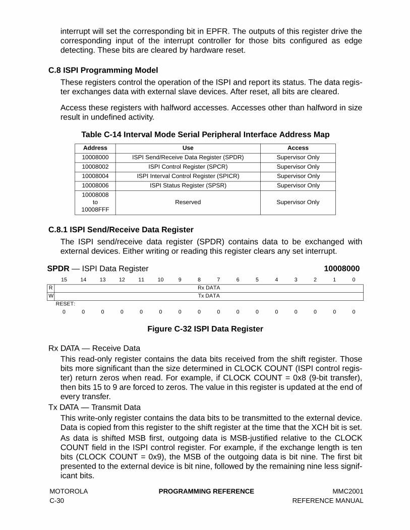
MOTOROLA PROGRAMMING REFERENCE MMC2001 C-30 REFERENCE MANUAL
interrupt will set the corresponding bit in EPFR. The outputs of this register drive thecorresponding input of the interrupt controller for those bits configured as edgedetecting. These bits are cleared by hardware reset.
C.8 ISPI Programming Model
These registers control the operation of the ISPI and report its status. The data regis-ter exchanges data with external slave devices. After reset, all bits are cleared.
Access these registers with halfword accesses. Accesses other than halfword in sizeresult in undefined activity.
C.8.1 ISPI Send/Receive Data Register
The ISPI send/receive data register (SPDR) contains data to be exchanged withexternal devices. Either writing or reading this register clears any set interrupt.
Figure C-32 ISPI Data Register
Rx DATA — Receive DataThis read-only register contains the data bits received from the shift register. Thosebits more significant than the size determined in CLOCK COUNT (ISPI control regis-ter) return zeros when read. For example, if CLOCK COUNT = 0x8 (9-bit transfer),then bits 15 to 9 are forced to zeros. The value in this register is updated at the end ofevery transfer.
Tx DATA — Transmit DataThis write-only register contains the data bits to be transmitted to the external device.Data is copied from this register to the shift register at the time that the XCH bit is set.As data is shifted MSB first, outgoing data is MSB-justified relative to the CLOCKCOUNT field in the ISPI control register. For example, if the exchange length is tenbits (CLOCK COUNT = 0x9), the MSB of the outgoing data is bit nine. The first bitpresented to the external device is bit nine, followed by the remaining nine less signif-icant bits.
Table C-14 Interval Mode Serial Peripheral Interface Address Map
Address Use Access
10008000 ISPI Send/Receive Data Register (SPDR) Supervisor Only
10008002 ISPI Control Register (SPCR) Supervisor Only
10008004 ISPI Interval Control Register (SPICR) Supervisor Only
10008006 ISPI Status Register (SPSR) Supervisor Only
10008008to
10008FFFReserved Supervisor Only
SPDR — ISPI Data Register 1000800015 14 13 12 11 10 9 8 7 6 5 4 3 2 1 0
R Rx DATA
W Tx DATA
RESET:
0 0 0 0 0 0 0 0 0 0 0 0 0 0 0 0

MMC2001 PROGRAMMING REFERENCE MOTOROLA REFERENCE MANUAL C-31
C.8.2 ISPI Control Register
The ISPI control register (SPCR), along with the ISPI interval control register, controlsthe operation of the ISPI. Follow this sequence when changing operating modes:
1. Disable the ISPI (COUNT = 0).
2. Wait for any transfer to complete (XCH bit clear).
3. Update to the new mode.
4. Re-enable the ISPI (COUNT = newcount).
Figure C-33 ISPI Control Register
DOZE — Doze ModeWhen the CPU executes a doze instruction and the system is placed in doze mode,the DOZE bit affects operation of the ISPI. When this bit is set, the ISPI is disabled indoze mode.
0 = ISPI unaffected in doze mode1 = ISPI disabled in doze mode
At reset, this bit is cleared to zero.
SPI_EN — ISPI EnableIn either master mode, this bit controls the value of the SPI_EN pin. The sense of theSPI_EN pin is determined by the SNS bit. In interval mode, the SPI_EN pin isasserted only when XCH is active. The SPI_EN bit must be programmed to a one forany master mode transfer to occur. In slave mode, the ISPI state machine uses theinput value on the SPI_EN pin, and this register bit is ignored. Further, the SPI_ENregister bit will not reflect the value of the SPI_EN pin in slave mode.
0 = Negated1 = Asserted
SNS — SPI_EN SenseThe SNS bit controls the sense of the SPI_EN pin relative to the SPI_EN register bitin the ISPI control register. This is required because in interval mode, the statemachine must assert and then negate the SPI_EN pin. The SNS bit has an affect onlywhen the SPI_EN pin is an output. If the SPI_EN pin is an input, then it is active low,and the SNS bit has no effect.
0 = SPI_EN pin is active low1 = SPI_EN pin is active high
SPCR — ISPI Control Register 1000800215 14 13 12 11 10 9 8 7 6 5 4 3 2 1 0
RDOZE
SPI_EN
SNS DRV MSTRIRQ_EN
PHA POL SPIGP BAUD RATE CLOCK COUNTW
RESET:
0 0 0 0 0 0 0 0 0 0 0 0 0 0 0 0

MOTOROLA PROGRAMMING REFERENCE MMC2001 C-32 REFERENCE MANUAL
DRV — Drive TypeThis bit controls the configuration of the SPI_CLK, SPI_EN and SPI_MOSI outputbuffers in either master mode of the ISPI (MSTR=1). In slave mode, this bit is ignored.
0 = Outputs are totem-pole while in either master mode1 = Outputs are open-drain while in either master mode
MSTR — Master ModeThis bit controls the mode of the ISPI. In slave mode, the SPI_CLK and SPI_EN pinsare inputs; in master modes, they are outputs.
0 = ISPI operates in slave mode1 = ISPI operates in either interval mode or manual mode (see IVL_EN in SICR)
IRQ_EN — Interrupt Request EnableThis bit enables/disables the ISPI interrupt request output signal. This bit is cleared tozero on reset.
0 = Interrupts disabled1 = Interrupts enabled
PHA — PhaseThis bit controls the phase shift of the SPI_CLK.
0 = Normal phase1 = Shift advance to opposite phase
POL — PolarityThis bit controls the polarity of the SPI_CLK.
0 = Normal polarity1 = Inverted polarity
SPIGP — SPI_GP ControlThis bit controls the data on the SPI_GP pin.
0 = Pin driven low1 = Pin driven high
BAUD RATEThese bits select the baud rate of the ISPI bit clock based on divisions of the systemclock. The master clock for the ISPI is HI_REFCLK.
Table C-15 BAUD RATE Values
Value Divide By
000 8
001 16
010 32
011 64
100 128
101 256
110 512
111 1024

MMC2001 PROGRAMMING REFERENCE MOTOROLA REFERENCE MANUAL C-33
CLOCK COUNTThese bits select the length of the transfer and control the justification of data. Fromtwo to 16 bits can be transferred. A count of all zeros causes the ISPI to be disabled.
C.8.3 ISPI Interval Control Register
The ISPI interval control register (SPICR) controls interval mode operation.
Figure C-34 ISPI Interval Control Register
LPBK — LoopbackThis bit enables a loopback test feature in the ISPI. When looping back, the ISPIoperates as if the SPI_MISO and SPI_MOSI pins are wired together and there are noother external devices connected to the ISPI data input pin. Whenever loopback isenabled, the data read from the ISPI data register after a given transfer matches whatwas written to the ISPI data register prior to that transfer, masked if necessary toaccount for the number of bits transferred.
0 = Loopback disabled1 = Loopback enabled
IVL_EN — Interval Mode EnableThis bit, when set, places the ISPI in interval mode. If the MSTR bit in the ISPI controlregister is cleared, then the ISPI is operating in slave mode, and this bit is ignored.
0 = ISPI is not operating in interval mode1 = ISPI is operating in interval mode if MSTR=1
INTERVAL COUNTIn interval mode, this register value is loaded into the ISPI interval timer upon comple-tion of a transfer. Each bit-clock period, the value in this counter is decremented byone. When the value in the register reaches zero, then XCH is set, and a new transferis begun.
Table C-16 CLOCK COUNT Values
Value Meaning
0000 Disable ISPI
0001 2-bit transfer
.
...
0111 8-bit transfer
.
...
1111 16-bit transfer
SPICR — ISPI Interval Control Register 1000800415 14 13 12 11 10 9 8 7 6 5 4 3 2 1 0
R 0LPBK
IVL_EN
INTERVAL COUNTW
RESET:
0 0 0 0 0 0 0 0 0 0 0 0 0 0 0 0
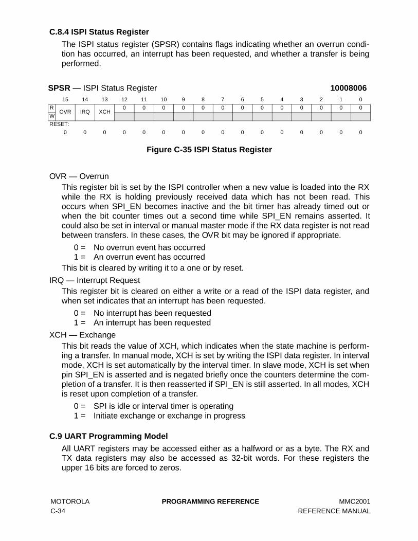
MOTOROLA PROGRAMMING REFERENCE MMC2001 C-34 REFERENCE MANUAL
C.8.4 ISPI Status Register
The ISPI status register (SPSR) contains flags indicating whether an overrun condi-tion has occurred, an interrupt has been requested, and whether a transfer is beingperformed.
Figure C-35 ISPI Status Register
OVR — OverrunThis register bit is set by the ISPI controller when a new value is loaded into the RXwhile the RX is holding previously received data which has not been read. Thisoccurs when SPI_EN becomes inactive and the bit timer has already timed out orwhen the bit counter times out a second time while SPI_EN remains asserted. Itcould also be set in interval or manual master mode if the RX data register is not readbetween transfers. In these cases, the OVR bit may be ignored if appropriate.
0 = No overrun event has occurred1 = An overrun event has occurred
This bit is cleared by writing it to a one or by reset.
IRQ — Interrupt RequestThis register bit is cleared on either a write or a read of the ISPI data register, andwhen set indicates that an interrupt has been requested.
0 = No interrupt has been requested1 = An interrupt has been requested
XCH — ExchangeThis bit reads the value of XCH, which indicates when the state machine is perform-ing a transfer. In manual mode, XCH is set by writing the ISPI data register. In intervalmode, XCH is set automatically by the interval timer. In slave mode, XCH is set whenpin SPI_EN is asserted and is negated briefly once the counters determine the com-pletion of a transfer. It is then reasserted if SPI_EN is still asserted. In all modes, XCHis reset upon completion of a transfer.
0 = SPI is idle or interval timer is operating1 = Initiate exchange or exchange in progress
C.9 UART Programming Model
All UART registers may be accessed either as a halfword or as a byte. The RX andTX data registers may also be accessed as 32-bit words. For these registers theupper 16 bits are forced to zeros.
SPSR — ISPI Status Register 1000800615 14 13 12 11 10 9 8 7 6 5 4 3 2 1 0
ROVR IRQ XCH
0 0 0 0 0 0 0 0 0 0 0 0 0
W
RESET:
0 0 0 0 0 0 0 0 0 0 0 0 0 0 0 0
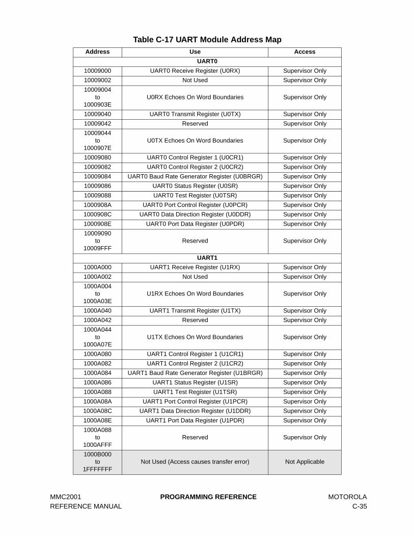
MMC2001 PROGRAMMING REFERENCE MOTOROLA REFERENCE MANUAL C-35
Table C-17 UART Module Address MapAddress Use Access
UART0
10009000 UART0 Receive Register (U0RX) Supervisor Only
10009002 Not Used Supervisor Only
10009004to
1000903EU0RX Echoes On Word Boundaries Supervisor Only
10009040 UART0 Transmit Register (U0TX) Supervisor Only
10009042 Reserved Supervisor Only
10009044to
1000907EU0TX Echoes On Word Boundaries Supervisor Only
10009080 UART0 Control Register 1 (U0CR1) Supervisor Only
10009082 UART0 Control Register 2 (U0CR2) Supervisor Only
10009084 UART0 Baud Rate Generator Register (U0BRGR) Supervisor Only
10009086 UART0 Status Register (U0SR) Supervisor Only
10009088 UART0 Test Register (U0TSR) Supervisor Only
1000908A UART0 Port Control Register (U0PCR) Supervisor Only
1000908C UART0 Data Direction Register (U0DDR) Supervisor Only
1000908E UART0 Port Data Register (U0PDR) Supervisor Only
10009090to
10009FFFReserved Supervisor Only
UART1
1000A000 UART1 Receive Register (U1RX) Supervisor Only
1000A002 Not Used Supervisor Only
1000A004to
1000A03EU1RX Echoes On Word Boundaries Supervisor Only
1000A040 UART1 Transmit Register (U1TX) Supervisor Only
1000A042 Reserved Supervisor Only
1000A044to
1000A07EU1TX Echoes On Word Boundaries Supervisor Only
1000A080 UART1 Control Register 1 (U1CR1) Supervisor Only
1000A082 UART1 Control Register 2 (U1CR2) Supervisor Only
1000A084 UART1 Baud Rate Generator Register (U1BRGR) Supervisor Only
1000A086 UART1 Status Register (U1SR) Supervisor Only
1000A088 UART1 Test Register (U1TSR) Supervisor Only
1000A08A UART1 Port Control Register (U1PCR) Supervisor Only
1000A08C UART1 Data Direction Register (U1DDR) Supervisor Only
1000A08E UART1 Port Data Register (U1PDR) Supervisor Only
1000A088to
1000AFFFReserved Supervisor Only
1000B000to
1FFFFFFFNot Used (Access causes transfer error) Not Applicable

MOTOROLA PROGRAMMING REFERENCE MMC2001 C-36 REFERENCE MANUAL
C.9.1 UART Receive Register (URX)
This read-only register contains received characters and status. After reset, if thereceiver is enabled (RXEN = 1), the CHARRDY bit is zero until the first character isreceived, and the remainder of the register contents are undefined. The RX register isechoed to 16-word addresses in order to support unloading the FIFO with the loadregister quadrant (ldq) instruction.
*Echoes begin at 10009004 and 1000A004 respectively.X = Undefined
Figure C-36 UART Receive Register
CHARRDY — Character ReadyThis read-only bit indicates whether the character in the RX DATA field and associ-ated flags are valid and ready to be read by the host.
0 = Character in RX DATA field and associated flags are invalid1 = Character in RX DATA field and associated flags valid and ready for reading
At reset, this bit is cleared to zero.
ERR — Error DetectWhen set, this read-only bit indicates that the character present in the RX DATA fieldhas an error status. The error can be an OVRRUN, FRMERR, BRK or PRERR. Thisbit is updated and valid for each received character.
0 = No error status detected1 = Error status detected
At reset, this bit is cleared to zero.
OVRRUN — Receiver OverrunWhen set, this read-only bit indicates that the receiver ignored data to prevent over-writing the data in the FIFO. Under normal circumstances, this bit should never beset. It indicates that the user’s software is not keeping up with the incoming data rate.This bit is updated and valid for each received character, and when set indicates thatsome number of characters were lost following the character for which the flag is set.
0 = No FIFO overrun1 = A FIFO overrun was detected
At reset, this bit is cleared to zero.
FRMERR — Frame ErrorWhen set, this read-only bit indicates that the current character had a framing error(missing stop bit). The data is possibly corrupted. This bit is updated for each charac-ter read from the FIFO.
U0RX — UART0 Receive Register 10009000*U1RX — UART1 Receive Register 1000A000*
15 14 13 12 11 10 9 8 7 6 5 4 3 2 1 0
RCHARRDY
ERROVRRUN
FRMERR
BRKPR
ERR0 0 RX DATA
W
RESET:
0 X X X X X X X X X X X X X X X

MMC2001 PROGRAMMING REFERENCE MOTOROLA REFERENCE MANUAL C-37
Every attempt has been made to allow the receiver to correctly interpret data follow-ing a character marked as having a framing error. (This includes ignoring the start bitvalidation logic, if appropriate.) However, when the transmitted data includes two stopbits, and both stop bits are incorrect, then the second stop bit will be interpreted asthe start bit of the next character.
0 = Character has no framing error1 = Character has a framing error
At reset, this bit is cleared to zero.
BRK — Break DetectWhen set, this read-only bit indicates that the current character was detected as abreak. The data bits are all zero and the stop bit is also zero. The frame error bit isalways set when this bit is set. When odd parity is selected, parity error is set whenthis bit is set. This bit is valid for each character read from the FIFO.
0 = Character is not a break character1 = Character is a break character
At reset, this bit is cleared to zero.
PRERR — Parity ErrorWhen set, this read-only bit indicates that the current character was detected with aparity error. The data is possibly corrupted. This bit is updated for each characterread from the FIFO. While parity is disabled, this bit always reads zero.
0 = No parity error detected for data in RX DATA field1 = Parity error detected for data in RX DATA field
At reset, this bit is cleared to zero.
RX DATA — Received DataThese read-only bits are the received character. In 7-bit mode, the MSB is forced tozero. In 8-bit mode, all bits are active.
C.9.2 UART Transmit Register (UTX)
The UART transmit register is used by the host to write the data to be transmitted.The low byte is write-only. When this register is read, bits TX[15:8] always return zero,and TX[7:0] is not driving the bus. The TX register is echoed to 16-word addresses inorder to support filling the transmit FIFO with the store register quadrant (stq) instruc-tion.
*Echoes begin at 10009044 and 1000A044 respectively.X = Undefined
Figure C-37 UART Transmit Register
U0TX — UART0 Transmit Register 10009040*U1TX — UART1 Transmit Register 1000A040*
15 14 13 12 11 10 9 8 7 6 5 4 3 2 1 0
R 0 0 0 0 0 0 0 0
W TX DATA
RESET:
0 0 0 0 0 0 0 0 X X X X X X X X

MOTOROLA PROGRAMMING REFERENCE MMC2001 C-38 REFERENCE MANUAL
TX DATA — Transmit DataThese write-only bits are the parallel transmit data inputs. In 7-bit mode, D7 isignored. In 8-bit mode, all bits are used. Data is transmitted LSB first. A new charac-ter is transmitted when these bits are written. These bits must be written only whileTRDY is high to ensure that corrupted data is not sent.
C.9.3 UART Control Register 1 (UCR1)
UART control register 1 is a read/write register. This register enables the UART andthe transmit and receive blocks. It controls the Tx and Rx FIFO levels and enables theTRDY and RRDY interrupts.
Figure C-38 UART Control Register 1
TxFL — Transmitter FIFO Interrupt Trigger LevelThese bits control the operation of the interrupt generated by the transmitter. Amaskable interrupt is generated whenever the data level in the TX FIFO drops belowthe selected threshold. The bits are encoded as follows:
At reset, these bits are cleared to zero.
TRDYEN — Transmitter Ready Interrupt EnableSetting this bit enables an interrupt when the transmitter has one or more slots avail-able in the TX FIFO. The fill level in the TX FIFO at which an interrupt is generated iscontrolled by the TxFL bits. While this bit is negated, the transmitter interrupt is dis-abled.
0 = TX interrupt disabled1 = TX interrupt enabled
At reset, this bit is cleared to zero.
TXEN — Transmitter EnableThis bit enables or disables the transmitter. While UARTEN and TXEN bits are set,and DOZE bit is cleared, the transmitter is enabled. If this bit is cleared in the middleof a transmission, the UART disables the transmitter immediately and starts markingones.
U0CR1 — UART0 Control Register 1 10009080U1CR1 — UART1 Control Register 1 1000A080
15 14 13 12 11 10 9 8 7 6 5 4 3 2 1 0
RTxFL
TRDY-EN
TXEN RxFLRRDY
ENRXEN IREN
0 RTSDEN
SND-BRK
0 0 DOZE
UARTENW
RESET:
0 0 0 0 0 0 0 0 0 0 0 0 0
Table C-18 TxFL Field Settings
Value Meaning00 Interrupt if TX FIFO has a slot for one or more character
01 Interrupt if TX FIFO has a slot for four or more characters
10 Interrupt if TX FIFO has a slot for eight or more characters
11 Interrupt if TX FIFO has a slot for fourteen or more characters
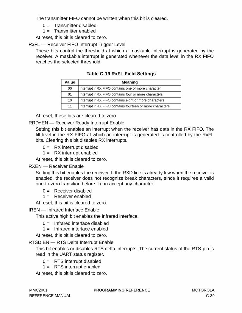
MMC2001 PROGRAMMING REFERENCE MOTOROLA REFERENCE MANUAL C-39
The transmitter FIFO cannot be written when this bit is cleared.
0 = Transmitter disabled1 = Transmitter enabled
At reset, this bit is cleared to zero.
RxFL — Receiver FIFO Interrupt Trigger LevelThese bits control the threshold at which a maskable interrupt is generated by thereceiver. A maskable interrupt is generated whenever the data level in the RX FIFOreaches the selected threshold.
At reset, these bits are cleared to zero.
RRDYEN — Receiver Ready Interrupt EnableSetting this bit enables an interrupt when the receiver has data in the RX FIFO. Thefill level in the RX FIFO at which an interrupt is generated is controlled by the RxFLbits. Clearing this bit disables RX interrupts.
0 = RX interrupt disabled1 = RX interrupt enabled
At reset, this bit is cleared to zero.
RXEN — Receiver EnableSetting this bit enables the receiver. If the RXD line is already low when the receiver isenabled, the receiver does not recognize break characters, since it requires a validone-to-zero transition before it can accept any character.
0 = Receiver disabled1 = Receiver enabled
At reset, this bit is cleared to zero.
IREN — Infrared Interface EnableThis active high bit enables the infrared interface.
0 = Infrared interface disabled1 = Infrared interface enabled
At reset, this bit is cleared to zero.
RTSD EN — RTS Delta Interrupt EnableThis bit enables or disables RTS delta interrupts. The current status of the RTS pin isread in the UART status register.
0 = RTS interrupt disabled1 = RTS interrupt enabled
At reset, this bit is cleared to zero.
Table C-19 RxFL Field Settings
Value Meaning
00 Interrupt if RX FIFO contains one or more character
01 Interrupt if RX FIFO contains four or more characters
10 Interrupt if RX FIFO contains eight or more characters
11 Interrupt if RX FIFO contains fourteen or more characters

MOTOROLA PROGRAMMING REFERENCE MMC2001 C-40 REFERENCE MANUAL
SNDBRK — Send BreakThis bit forces the transmitter to send a break character. The transmitter will finishsending the character in progress (if any) and then send break characters until this bitis reset. The user is responsible for ensuring that this bit is high for a sufficient periodof time to generate a valid break; the transmitter samples SNDBRK after every bit istransmitted.
Following completion of the break transmission, the UART transmits two mark bits.The user can continue to fill the FIFO, and any characters remaining will be transmit-ted when the break is terminated. This bit cannot be changed until the UART EN andTX EN bits in the UART control register 1 (UxCR1) are set.
0 = Do not send break1 = Send break (continuous zeros)
At reset, this bit is cleared to zero.
DOZE When the CPU executes a doze instruction and the system is placed in the dozemode, the DOZE bit affects operation of the UART. If this bit is set when the system isin the doze mode, the UART is disabled.
0 = UART unaffected while the MCU is in doze mode1 = UART disabled while the MCU is in doze mode
At reset, this bit is cleared to zero.
UART EN — UART EnableThis bit enables or disables the UART. If this bit is cleared in the middle of a transmis-sion, the transmitter stops and drives the TXD line to logic one.
0 = UART disabled1 = UART enabled
At reset, this bit is cleared to zero.
C.9.4 UART Control Register 2 (UCR2)
UART control register 2 is a read/write register. This register controls the overall oper-ation of the UART. It controls the clock source, number of bits per character, paritygeneration and checking, and behavior of the RTS, CTS, and DTR pins.
Figure C-39 UART Control Register 2
U0CR2 — UART0 Control Register 2 10009082U1CR2 — UART1 Control Register 2 1000A082
15 14 13 12 11 10 9 8 7 6 5 4 3 2 1 0
R 0 IRTS CTSC CTS 0 0 0 PREN PROE STPB WS 0 0 0 0 0
W
RESET:
0 0 0 0 0 0 0 0

MMC2001 PROGRAMMING REFERENCE MOTOROLA REFERENCE MANUAL C-41
IRTS — Ignore RTSSetting this bit forces the RTS input signal presented to the transmitter to always beasserted, effectively causing the external pin to be ignored. In this mode, the RTS pincan be used as a general-purpose input.
0 = Transmit only while RTS pin is asserted1 = Ignore RTS pin
At reset, this bit is cleared to zero.
CTSC — CTS Pin ControlThis bit controls the operation of the CTS output pin. While this bit is set, the CTS out-put pin is controlled by the receiver. When the RX FIFO has a pending overrun, theCTS output pin is negated to indicate to the far-end transmitter to stop transmitting.While the CTSC bit is negated, the CTS output pin is controlled by the CTS bit. On reset, since this bit is cleared to zero, the CTS pin is controlled by the CTS bit,which is also cleared to zero on reset. This means that on reset the CTS signal isnegated.
0 = CTS pin controlled by the CTS bit1 = CTS pin controlled by the receiver
At reset, this bit is cleared to zero.
CTS — CTS bitThis bit controls the CTS pin while the CTSC bit is negated. While CTSC is assertedthis bit has no function.
0 = CTS pin is driven high (inactive)1 = CTS pin is driven low (active)
At reset, this bit is cleared to zero.PREN — Parity Enable
This bit enables or disables the parity generator in the transmitter and parity checkerin the receiver.
0 = Parity disabled1 = Parity enabled
At reset, this bit is cleared to zero.PROE — Parity Odd/Even
This bit controls the sense of the parity generator and checker. When PROE is set,odd parity is generated and expected. When PROE is cleared, even parity is gener-ated and expected. This bit has no function if PREN is low.
0 = Even parity 1 = Odd parity
At reset, this bit is cleared to zero.STPB — Stop Bits
This bit controls the number of stop bits transmitted after a character. When STPB isset, two stop bits are sent. When STPB is cleared, one stop bit is sent. This bit has noeffect on the receiver, which expects one or more stop bits.
0 = One stop bit transmitted1 = Two stop bits transmitted
At reset, this bit is cleared to zero.

MOTOROLA PROGRAMMING REFERENCE MMC2001 C-42 REFERENCE MANUAL
WS — Word SizeThis bit specifies a character length of eight or seven bits (not including start, stop, orparity bits). When WS is set, the transmitter and receiver are in eight-bit mode. WhenWS is cleared, they are in seven-bit mode. The transmitter then ignores B7, and thereceiver sets B7 to zero. This bit can be changed between transmissions or recep-tions. If it is changed while a transmission or reception is in progress, however, thelength of the current character being transmitted or received is unpredictable.
0 = 7-bit transmit and receive character length1 = 8-bit transmit and receive character length
At reset, this bit is cleared to zero.
C.9.5 UART BRG Register (UBRGR)
This register specifies the divide ratio of the prescaler in the UART bit clock genera-tor.
Figure C-40 UART BRG Register
CD — Clock DividerThese bits determine the bit clock generator output rate. The CD field is used to pre-set a 12-bit counter that is decremented at the system clock rate. The value 0x000produces the maximum clock rate (equal to the system clock). The value 0xFFF pro-duces the minimum clock rate (divide by 4096).
C.9.6 UART Status Register (USR)
The read/write UART status register indicates the status of the RTS pin, input transi-tions on the pin, and status of the transmit and receive FIFOs.
Figure C-41 UART Status Register
U0BRGR — UART0 BRG Register 10009084U1BRGR — UART1 BRG Register 1000A084
15 14 13 12 11 10 9 8 7 6 5 4 3 2 1 0
R 0 0 0 0CD
W
RESET:
0 0 0 0 0 0 0 0 0 0 0 0
U0SR — UART0 Status Register 10009086U1SR — UART1 Status Register 1000A086
15 14 13 12 11 10 9 8 7 6 5 4 3 2 1 0
RTX
MPTYRTSS TRDY 0 0 0 RRDY 0 0 0
RTSD0 0 0 0 0
W
RESET:
1 0 1 0 0

MMC2001 PROGRAMMING REFERENCE MOTOROLA REFERENCE MANUAL C-43
TXMPTY — Transmitter EmptyWhen set, this bit indicates that the transmit FIFO and the transmit shift register areboth empty. This bit is automatically cleared when a write to the TX FIFO is per-formed.
0 = TX FIFO or shifter are not both empty1 = TX FIFO and shifter are both empty
At reset, this bit is set to one.
RTSS — RTS Pin StatusThis bit indicates the current status of the RTS pin. A “snapshot” of the pin is takenimmediately before this bit is presented to the data bus. While IRTS is asserted, thisbit can be used as a general-purpose input.
0 = RTS pin is high (inactive)1 = RTS pin is low (active)
This bit follows the logic value connected to the RTS pin.
TRDY — Transmitter Ready Interrupt FlagWhen set, this bit indicates that the TX FIFO has emptied below its target thresholdand needs data. This bit is automatically cleared when the data level in the TX FIFOgoes beyond the set threshold level.
0 = Transmitter does not need data1 = Transmitter needs data (interrupt posted)
At reset, this bit is set to one.
RRDY — Receiver Ready Interrupt FlagWhen set, this bit indicates that the receive FIFO data level is above the thresholdlevel specified by the RxFL field, and a maskable interrupt is generated. Refer to theRxFL bit description for setting the threshold level. In conjunction with the CHARRDYbit, host software can continue to read the RX FIFO in an interrupt service routineuntil the RX FIFO is empty. This bit is automatically cleared when the data level in theRX FIFO goes below the set threshold level.
0 = No character ready (no interrupt posted)1 = Character(s) ready (interrupt posted)
At reset, this bit is cleared to zero.
RTSD — RTS DeltaWhen set, this bit indicates that the RTS pin changed state. It generates a maskableinterrupt. In STOP mode, RTS assertion sets this bit to wake the CPU. The currentstate of the RTS pin is available in the RTSS bit. The RTSD interrupt is cleared bywriting a one to this bit.
0 = RTS pin did not change state since last cleared1 = RTS pin changed state
At reset, this bit is cleared to zero.
C.9.7 UART Test Register (UTSR)
The UART test register is a read/write register. Unimplemented bits always returnzero when read. This register contains miscellaneous bits to control test features ofthe UART block.

MOTOROLA PROGRAMMING REFERENCE MMC2001 C-44 REFERENCE MANUAL
Figure C-42 UART Test Register
FRC PERR — Force Parity ErrorWhen set, this bit forces the transmitter to generate a parity error if parity is enabled.This bit is provided for system debugging.
0 = Generate normal parity1 = Generate inverted parity (error)
At reset, this bit is cleared to zero.
LOOP — Loop TX and RX for TestThis bit controls loopback for test purposes. When this bit is high, the receiver input isinternally connected to the transmitter and ignores the RxD pin. The transmitter isunaffected by this bit. This loopback operates to connect the data on the TxD pindirectly to the voting logic. If infrared mode is enabled (IR_EN is active), the effect ofactivating this bit is to put an IR-formatted bit stream into the voting logic, which willyield odd results. Do not use this loopback if IR_EN is active.
0 = Normal receiver operation1 = Internal connect transmitter output to receiver input
At reset, this bit is cleared to zero.
LOOP IR — Loop TX and RX for IR TestThis bit controls a loopback from transmitter to receiver in the infrared interface.
0 = No IR loop1 = Connect IR transmit to IR receiver
At reset, this bit is cleared to zero.
C.9.8 UART Port Control Register (UPCR)
The read/write UART port control register controls the functionality of UART GPIOpins.
Figure C-43 UART Port Control Register
U0TSR — UART0 Test Register 10009088U1TSR — UART1 Test Register 1000A088
15 14 13 12 11 10 9 8 7 6 5 4 3 2 1 0
R 0 0 FRC
PERRLOOP
0 LOOP
IR
0 0 0 0 0 0 0 0 0 0
W
RESET:
0 0 0 0 0 0 0 0 0 0 0 0 0 0 0 0
U0PCR — UART0 Port Control Register 1000908AU1PCR — UART1 Port Control Register 1000A08A
15 14 13 12 11 10 9 8 7 6 5 4 3 2 1 0
R 0 0 0 0 0 0 0 0 0 0 0 0PC3 PC2 PC1 PC0
W
RESET:
0 0 0 0
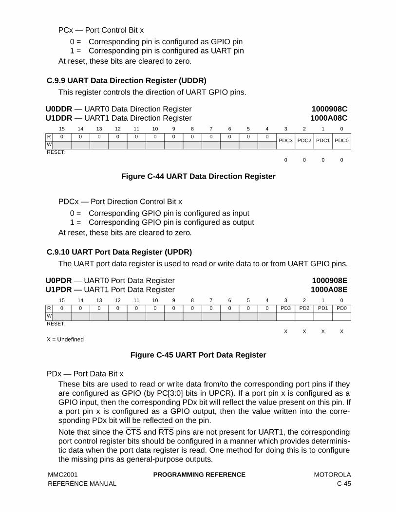
MMC2001 PROGRAMMING REFERENCE MOTOROLA REFERENCE MANUAL C-45
PCx — Port Control Bit x
0 = Corresponding pin is configured as GPIO pin1 = Corresponding pin is configured as UART pin
At reset, these bits are cleared to zero.
C.9.9 UART Data Direction Register (UDDR)
This register controls the direction of UART GPIO pins.
Figure C-44 UART Data Direction Register
PDCx — Port Direction Control Bit x
0 = Corresponding GPIO pin is configured as input1 = Corresponding GPIO pin is configured as output
At reset, these bits are cleared to zero.
C.9.10 UART Port Data Register (UPDR)
The UART port data register is used to read or write data to or from UART GPIO pins.
X = Undefined
Figure C-45 UART Port Data Register
PDx — Port Data Bit x These bits are used to read or write data from/to the corresponding port pins if theyare configured as GPIO (by PC[3:0] bits in UPCR). If a port pin x is configured as aGPIO input, then the corresponding PDx bit will reflect the value present on this pin. Ifa port pin x is configured as a GPIO output, then the value written into the corre-sponding PDx bit will be reflected on the pin.
Note that since the CTS and RTS pins are not present for UART1, the correspondingport control register bits should be configured in a manner which provides determinis-tic data when the port data register is read. One method for doing this is to configurethe missing pins as general-purpose outputs.
U0DDR — UART0 Data Direction Register 1000908CU1DDR — UART1 Data Direction Register 1000A08C
15 14 13 12 11 10 9 8 7 6 5 4 3 2 1 0
R 0 0 0 0 0 0 0 0 0 0 0 0PDC3 PDC2 PDC1 PDC0
W
RESET:
0 0 0 0
U0PDR — UART0 Port Data Register 1000908EU1PDR — UART1 Port Data Register 1000A08E
15 14 13 12 11 10 9 8 7 6 5 4 3 2 1 0
R 0 0 0 0 0 0 0 0 0 0 0 0 PD3 PD2 PD1 PD0
W
RESET:
X X X X
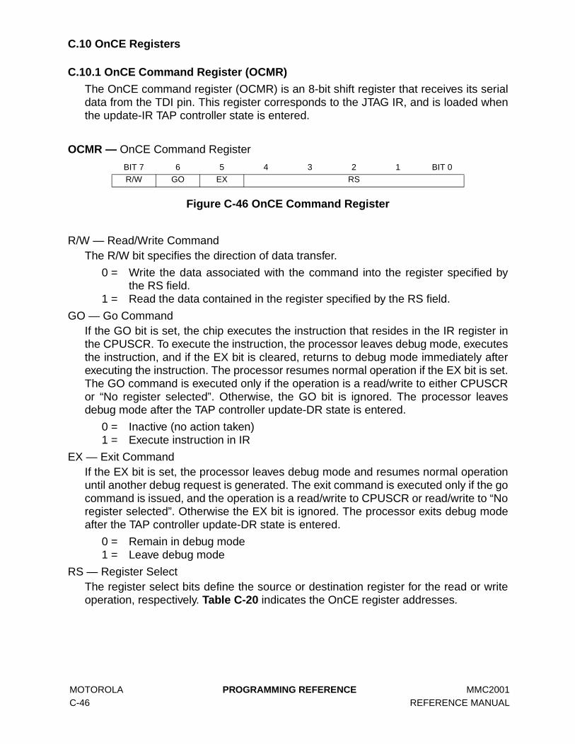
MOTOROLA PROGRAMMING REFERENCE MMC2001 C-46 REFERENCE MANUAL
C.10 OnCE Registers
C.10.1 OnCE Command Register (OCMR)
The OnCE command register (OCMR) is an 8-bit shift register that receives its serialdata from the TDI pin. This register corresponds to the JTAG IR, and is loaded whenthe update-IR TAP controller state is entered.
Figure C-46 OnCE Command Register
R/W — Read/Write CommandThe R/W bit specifies the direction of data transfer.
0 = Write the data associated with the command into the register specified bythe RS field.
1 = Read the data contained in the register specified by the RS field.
GO — Go CommandIf the GO bit is set, the chip executes the instruction that resides in the IR register inthe CPUSCR. To execute the instruction, the processor leaves debug mode, executesthe instruction, and if the EX bit is cleared, returns to debug mode immediately afterexecuting the instruction. The processor resumes normal operation if the EX bit is set.The GO command is executed only if the operation is a read/write to either CPUSCRor “No register selected”. Otherwise, the GO bit is ignored. The processor leavesdebug mode after the TAP controller update-DR state is entered.
0 = Inactive (no action taken)1 = Execute instruction in IR
EX — Exit CommandIf the EX bit is set, the processor leaves debug mode and resumes normal operationuntil another debug request is generated. The exit command is executed only if the gocommand is issued, and the operation is a read/write to CPUSCR or read/write to “Noregister selected”. Otherwise the EX bit is ignored. The processor exits debug modeafter the TAP controller update-DR state is entered.
0 = Remain in debug mode1 = Leave debug mode
RS — Register Select The register select bits define the source or destination register for the read or writeoperation, respectively. Table C-20 indicates the OnCE register addresses.
OCMR — OnCE Command Register
BIT 7 6 5 4 3 2 1 BIT 0R/W GO EX RS

MMC2001 PROGRAMMING REFERENCE MOTOROLA REFERENCE MANUAL C-47
C.10.2 OnCE Control Register (OCR)
The OnCE control register (OCR) is a 32-bit register used to select the events that putthe chip in debug mode and to enable or disable sections of the OnCE logic. The con-trol bits are read/write.
Figure C-47 OnCE Control Register
Table C-20 OnCE Register Addressing
RS Register Selected
00000 Reserved
00001 Reserved
00010 Reserved
00011 Trace Counter (OTC)
00100 Memory Breakpoint Counter A (MBCA)
00101 Memory Breakpoint Counter B (MBCB)
00110 Program Counter FIFO and Increment Counter
00111 Breakpoint Address Base Register A (BABA)
01000 Breakpoint Address Base Register B (BABB)
01001 Breakpoint Address Mask Register A (BAMA)
01010 Breakpoint Address Mask Register B (BAMB)
01011 CPU Scan Register (CPUSCR)
01100 No Register Selected (Bypass)
01101 OnCE Control Register (OCR)
01110 OnCE Status Register (OSR)
01111 Reserved (Factory Test Control Register — do not access)
10000 Reserved (MEM_BIST, do not access)
10001 – 10110 Reserved (Bypass, do not access)
10111 Reserved (LSRL, do not access)
11000 – 11110 Reserved (Bypass, do not access)
11111 Bypass
OCR — OnCE Control Register31 30 29 28 27 26 25 24 23 22 21 20 19 18 17 16
R 0 0 0 0 0 0 0 0 0 0 0 0 0 0SQC
W
RESET:
0 0
15 14 13 12 11 10 9 8 7 6 5 4 3 2 1 0
RDR IDRE TME FRZC RCB BCB RCA BCA
W
RESET:
0 0 0 0 0 0 0 0 0 0 0 0 0 0 0 0

MOTOROLA PROGRAMMING REFERENCE MMC2001 C-48 REFERENCE MANUAL
SQC — Sequential ControlThe SQC field allows memory breakpoint B and trace occurrences to be suspendeduntil a qualifying event occurs. This field is cleared on test logic reset.
DR — CPU Debug Request ControlThis control bit is used to request the CPU to enter debug mode unconditionally. TheCPU indicates that debug mode has been entered via the PM bits in the OnCE statusregister. Once the CPU enters debug mode, it returns there even with a write to theOCMR with GO and EX set until the DR bit is cleared. This bit is cleared on test logicreset.
IDRE — Internal Debug Request EnableThis control bit is used to enable internally generated debug requests. The internaldebug request input to the OnCE control logic (IDR) may not be used in all implemen-tations. In some implementations, the IDR control input may be connected and usedas an additional hardware debug request. This bit is cleared on test logic reset.
0 = Disable IDR input operation1 = Enable IDR input operation
TME — Trace Mode EnableThe TME control bit enables the OnCE trace mode operation. This bit is cleared ontest logic reset. Trace operation is also affected by the SQC field described above.
0 = Disable trace operation1 = Enable trace operation
FRZC — Freeze ControlThis control bit is used in conjunction with memory breakpoint B registers to selectbetween asserting a breakpoint condition when a memory breakpoint B occurs, orfreezing the PC FIFO from further updates when memory breakpoint B occurs whileallowing the CPU to continue execution. The PC FIFO remains frozen until the FRZObit in the OSR is cleared.
Table C-21 Sequential Control Field Definition
SQC[1:0] Meaning
00Disable sequential control operation. Memory breakpoints and trace operation are unaf-fected by this field.
01
Suspend normal trace counter operation until a breakpoint condition occurs for memory breakpoint B. When this mode is selected, memory breakpoint B occurrences no longer cause a breakpoint request to be generated. Instead, trace counter comparisons are sus-pended until the first memory breakpoint B occurrence. After the first memory breakpoint B occurrence, trace counter control is released to perform normally (assuming TME is set). This allows a sequence of breakpoint conditions to be specified prior to trace count-ing.
10
Qualify memory breakpoint B matches with a breakpoint occurrence for memory break-point A. When this bit is set, memory breakpoint A occurrences no longer cause a break-point request to be generated. Instead, memory breakpoint B comparisons are suspended until the first memory breakpoint A occurrence. After the first memory break-point A occurrence, memory breakpoint B is enabled to perform normally. This allows a sequence of breakpoint conditions to be specified.
11
Combine the qualifications specified by the 01 and 10 encodings of this field. In this mode, no breakpoint requests are generated, and trace count operation is enabled (when TME is set) once a memory breakpoint B occurrence follows a memory breakpoint A occurrence.
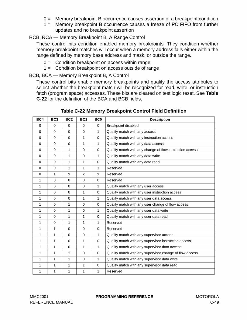
MMC2001 PROGRAMMING REFERENCE MOTOROLA REFERENCE MANUAL C-49
0 = Memory breakpoint B occurrence causes assertion of a breakpoint condition1 = Memory breakpoint B occurrence causes a freeze of PC FIFO from further
updates and no breakpoint assertion
RCB, RCA — Memory Breakpoint B, A Range Control These control bits condition enabled memory breakpoints. They condition whethermemory breakpoint matches will occur when a memory address falls either within therange defined by memory base address and mask, or outside the range.
0 = Condition breakpoint on access within range1 = Condition breakpoint on access outside of range
BCB, BCA — Memory Breakpoint B, A Control These control bits enable memory breakpoints and qualify the access attributes toselect whether the breakpoint match will be recognized for read, write, or instructionfetch (program space) accesses. These bits are cleared on test logic reset. See TableC-22 for the definition of the BCA and BCB fields.
Table C-22 Memory Breakpoint Control Field Definition
BC4 BC3 BC2 BC1 BC0 Description
0 0 0 0 0 Breakpoint disabled
0 0 0 0 1 Qualify match with any access
0 0 0 1 0 Qualify match with any instruction access
0 0 0 1 1 Qualify match with any data access
0 0 1 0 0 Qualify match with any change of flow instruction access
0 0 1 0 1 Qualify match with any data write
0 0 1 1 0 Qualify match with any data read
0 0 1 1 1 Reserved
0 1 x x x Reserved
1 0 0 0 0 Reserved
1 0 0 0 1 Qualify match with any user access
1 0 0 1 0 Qualify match with any user instruction access
1 0 0 1 1 Qualify match with any user data access
1 0 1 0 0 Qualify match with any user change of flow access
1 0 1 0 1 Qualify match with any user data write
1 0 1 1 0 Qualify match with any user data read
1 0 1 1 1 Reserved
1 1 0 0 0 Reserved
1 1 0 0 1 Qualify match with any supervisor access
1 1 0 1 0 Qualify match with any supervisor instruction access
1 1 0 1 1 Qualify match with any supervisor data access
1 1 1 0 0 Qualify match with any supervisor change of flow access
1 1 1 0 1 Qualify match with any supervisor data write
1 1 1 1 0 Qualify match with any supervisor data read
1 1 1 1 1 Reserved

MOTOROLA PROGRAMMING REFERENCE MMC2001 C-50 REFERENCE MANUAL
C.10.3 OnCE Status Register (OSR)
The OnCE status register (OSR) is a 16-bit register used to indicate the reason(s)that debug mode was entered and the current operating mode of the CPU. These sta-tus bits are read only.
Figure C-48 OnCE Status Register
HDRO — Hardware Debug Request Occurrence This read-only status bit is set when the processor enters debug mode as a result ofa hardware debug request from the IDR signal or the DE pin. This bit is cleared ontest logic reset or when debug mode is exited with the GO and EX bits set.
DRO — Debug Request OccurrenceThis read-only status bit is set when the processor enters debug mode and the debugrequest (DR) control bit in the OnCE control register is set. This bit is cleared on testlogic reset or when debug mode is exited with the GO and EX bits set.
MBO — Memory Breakpoint OccurrenceThis read-only status bit is set when a memory breakpoint request has been issued tothe CPU via the BRKRQ input and the CPU enters debug mode. In some situationsinvolving breakpoint requests on instruction prefetches, the CPU may discard therequest along with the prefetch. In this case, this bit may become set due to the CPUentering debug mode for another reason. This bit is cleared on test logic reset orwhen debug mode is exited with the GO and EX bits set.
SWO — Software Debug OccurrenceThis read-only status bit is set when the processor enters debug mode of operationas a result of the execution of the bkpt instruction. This bit is cleared on test logicreset or when debug mode is exited with the GO and EX bits set.
TO — Trace Count OccurrenceThis read-only status bit is set when the trace counter reaches zero with the tracemode enabled and the CPU enters debug mode. This bit is cleared on test logic resetor when debug mode is exited with the GO and EX bits set.
FRZO — FIFO Freeze OccurrenceThis read-only status bit is set when a FIFO freeze occurs. This bit is cleared on testlogic reset or when debug mode is exited with the GO and EX bits set.
SQB — Sequential Breakpoint B Arm OccurrenceThis read-only status bit is set when sequential operation is enabled and a memorybreakpoint B event has occurred to enable trace counter operation. This bit is clearedon test logic reset or when debug mode is exited with the GO and EX bits set.
OSR — OnCE Status Register 15 14 13 12 11 10 9 8 7 6 5 4 3 2 1 0
R 0 0 0 0 0 0 HDRO DRO MBO SWO TO FRZO SQB SQA PM
W
RESET: 0 0 0 0 0 0 0 0 0 0
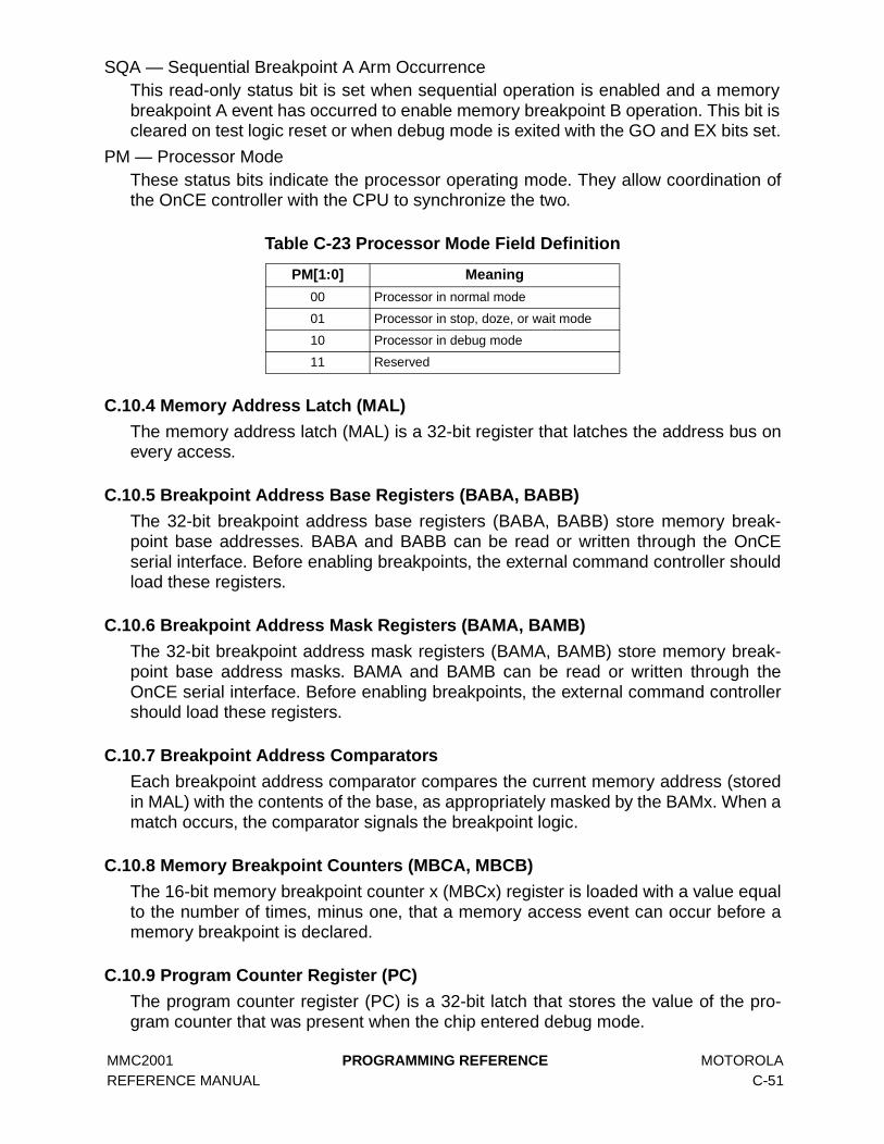
MMC2001 PROGRAMMING REFERENCE MOTOROLA REFERENCE MANUAL C-51
SQA — Sequential Breakpoint A Arm OccurrenceThis read-only status bit is set when sequential operation is enabled and a memorybreakpoint A event has occurred to enable memory breakpoint B operation. This bit iscleared on test logic reset or when debug mode is exited with the GO and EX bits set.
PM — Processor ModeThese status bits indicate the processor operating mode. They allow coordination ofthe OnCE controller with the CPU to synchronize the two.
C.10.4 Memory Address Latch (MAL)
The memory address latch (MAL) is a 32-bit register that latches the address bus onevery access.
C.10.5 Breakpoint Address Base Registers (BABA, BABB)
The 32-bit breakpoint address base registers (BABA, BABB) store memory break-point base addresses. BABA and BABB can be read or written through the OnCEserial interface. Before enabling breakpoints, the external command controller shouldload these registers.
C.10.6 Breakpoint Address Mask Registers (BAMA, BAMB)
The 32-bit breakpoint address mask registers (BAMA, BAMB) store memory break-point base address masks. BAMA and BAMB can be read or written through theOnCE serial interface. Before enabling breakpoints, the external command controllershould load these registers.
C.10.7 Breakpoint Address Comparators
Each breakpoint address comparator compares the current memory address (storedin MAL) with the contents of the base, as appropriately masked by the BAMx. When amatch occurs, the comparator signals the breakpoint logic.
C.10.8 Memory Breakpoint Counters (MBCA, MBCB)
The 16-bit memory breakpoint counter x (MBCx) register is loaded with a value equalto the number of times, minus one, that a memory access event can occur before amemory breakpoint is declared.
C.10.9 Program Counter Register (PC)
The program counter register (PC) is a 32-bit latch that stores the value of the pro-gram counter that was present when the chip entered debug mode.
Table C-23 Processor Mode Field Definition
PM[1:0] Meaning
00 Processor in normal mode
01 Processor in stop, doze, or wait mode
10 Processor in debug mode
11 Reserved

MOTOROLA PROGRAMMING REFERENCE MMC2001 C-52 REFERENCE MANUAL
C.10.10 Instruction Register (IR)
The instruction register (IR) provides a mechanism for controlling the debug sessionby forcing in selected instructions and then causing them to be executed in a con-trolled manner by the debug control block.
C.10.11 Control State Register (CTL)
The control state register (CTL) is used to set control values when debug mode isexited. On scan-in, this register is used to control specific aspects of the CPU. Certainbits reflect internal processor status and should be restored to their original values.
The CTL is a 16-bit latch that stores the value of certain internal CPU state variablesbefore debug mode is entered. This register is affected by the operations performedduring the debug session and should be restored by the external command controllerwhen returning to normal mode. In addition to saved internal state variables, the bitsare used by emulation firmware to control the debug process.
Set reserved bits to ones.
Figure C-49 Control State Register
FFY — Feed Forward Y Operand This control bit is used to force the content of the WBBR to be used as the Y operandvalue of the first instruction to be executed following an update of the CPUSCR. Thisgives the debug firmware the capability of updating processor registers by initializingthe WBBR with the desired value, setting the FFY bit, and executing a mov instruc-tion to the desired register.
FDB — Force PSR Debug Mode A logical OR of this control bit with the PSR(DB) bit determines whether the proces-sor is operating in debug enable mode or not. The processor can be placed in debugenable mode by setting this bit regardless of the state of the PSR(DB) bit. In debugenable mode, execution of the bkpt instruction as well as recognition of the BRKRQinput cause the processor to enter debug mode, as if the DBGRQ input had beenasserted.
SZ — Prefetch Size This control field is used to drive the CPU SIZ[1:0] outputs on the first instructionprefetch caused by issuing a OnCE command with the GO bit set and not ignored. Itshould be set to indicate a 16-bit size, i.e., 0b10. This field should be restored to itsoriginal value after a debug session is completed, i.e., when a OnCE command isissued with the GO and EX bits set and not ignored.
CTL — Control State Register 15 14 13 12 11 10 9 8 7 6 5 4 3 2 1 0
RReserved FFY FDB SZ TC Reserved
W
RESET:
0 0 0 0 0 0 0

MMC2001 PROGRAMMING REFERENCE MOTOROLA REFERENCE MANUAL C-53
TC — Prefetch Transfer CodeThis control field is used to drive the CPU TC[2:0] outputs on the first instructionprefetch caused by issuing a OnCE command with the GO bit set and not ignored. Itshould typically be set to indicate a supervisor instruction access, i.e., 0b110. Thisfield should be restored to its original value after a debug session is completed, i.e.,when a OnCE command is issued with the GO and EX bits set and not ignored.
C.10.12 Write-Back Bus Register (WBBR)
The write-back bus register (WBBR) is used as a means of passing operand informa-tion between the CPU and the external command controller.
To update a processor resource, this register is initialized with a data value to be writ-ten, and a mov instruction is executed which uses this value as a write-back datavalue. The FFY bit in the control state register forces the value of the WBBR to besubstituted for the normal source value of a mov instruction, thus allowing updates toprocessor registers to be performed.
C.10.13 Processor Status Register (PSR)
The OnCE processor status register (PSR) is a 32-bit latch used to read or write theM•CORE processor status register. Whenever the external command controllerneeds to save or modify the contents of the M•CORE processor status register, thisregister is used. This register is affected by the operations performed in debug modeand must be restored by the external command controller when returning to normalmode.
C.10.14 Reserved Test Control Registers (Reserved, MEM_BIST, FTCR, LSRL)
These registers are reserved for factory testing.
WARNINGTo prevent damage to the device or system, do not access theseregisters during normal operation.

MOTOROLA PROGRAMMING REFERENCE MMC2001 C-54 REFERENCE MANUAL

MMC2001 MOTOROLA
REFERENCE MANUAL I-1
–A–
AC electrical specifications A-2ADDR (address bus) signals 4-4, 7-1Address bus 4-4, 7-1AE bit 9-5, C-7AF bit 2-4AIE bit 9-5, 9-6, C-7AIF bit 9-5, 9-6, C-7Alarm Enable bit 9-5, C-7Alarm Interrupt Enable bit 9-5, 9-6, C-7Alarm Interrupt Flag 9-5, 9-6, C-7Alternate file 2-3Alternate File bit 2-4
–B–
BABA 16-14, C-51BABB 16-14, C-51BACA 16-14, C-51BACB 16-14, C-51BAMA 16-14, C-51BAMB 16-14, C-51BAUD RATE field 12-7, C-32BCA bit 16-10, C-49BCB bit 16-10, C-49Big-endian byte ordering 2-5Bit clock generator 11-4Bit time 11-4Boot mode 4-4, 7-2, 7-6Break Detect bit 11-8, C-37Break frame 11-3, 11-4Breakpoint
Address Base Registers 16-14, C-51Address Comparators 16-14, C-51Address Mask Registers 16-14, C-51logic 16-12
BRK bit 11-8, C-37BRKRQ signal 16-5Bus sizing 7-4Bus watchdog 7-6
–C–
C bit 2-3CD bit 11-13, C-42CHARRDY bit 11-7, C-36Chip Select 4-4, 7-2
Assert bit 7-9, C-18Control Registers 7-7, C-16
Enable bit 7-11, C-20CKOE bit 8-7, 9-4, C-6CKOS bit 9-3, C-6Clear to send 4-7, 11-2CLK SEL field 15-6, C-25CLKIN signal 4-5CLKOUT Enable bit 8-7, 9-4, C-6CLKOUT signal 4-5, 8-7CLKOUT Source bit 9-3, C-6CLKSRC bit 11-13Clock
Divider bit 11-13, C-42input 4-5input specifications A-2module 8-1
block diagram 8-3output 4-5, 8-7Select field 15-6, C-25source 8-1Source bit 11-13
CLOCK COUNT field 12-7, C-33Column strobes 4-7Condition Code/Carry bit 2-3Control registers 2-3Control State Register 16-18, C-52COUNT EN bit 15-5, C-25COUNT field 15-7, C-27Counter Enable bit 15-5, C-25Counter Overwrite Enable bit 9-14, C-12Counter Reload Control bit 9-12, 9-13, 9-15, C-12CPU
breakpoint request 16-5debug acknowledge 16-5debug request 16-5Debug Request Control bit 16-9, C-48status signals 16-5
Crystal oscillator 4-5CS signals 4-4, 7-2CSA bit 7-9, C-18CSEN bit 7-11, C-20CSxCR 7-7, C-16CTL 16-18, C-52CTS bit 11-12, C-41CTS Pin Control bit 11-12, C-41CTS signal 11-2CTS0 4-7CTSC bit 11-12, C-41
–D–
DATA (data bus) signals 4-4, 7-2
INDEX

MOTOROLA MMC2001
I-2 REFERENCE MANUAL
DATA bit 15-5, C-24Data bus 4-4, 7-2Data organization
in memory 2-5in registers 2-5
Data Port Size bit 7-10, C-19DBG bit 9-14, C-11DBGACK signal 16-5DBGRQ signal 16-5DC electrical specifications A-1DE signal 4-6, 16-4Debug
event 4-6, 16-4mode
entering 16-16ISP 12-11select 16-3UART 11-24
Mode Control bit 9-14, C-11Request Occurrence bit 16-11, C-50serial clock 16-3serial input 16-3serial output 16-3
DEBUG signal 16-6DIR bit 15-5, C-24Direction bit 15-5, C-24DOZE bit
ISPI 12-6, C-31PIT 9-14, C-11PWM 15-4, C-23UART 11-11, C-40
Doze mode 8-4DR bit 16-9, C-48Drive Type bit 12-6, C-32DRO bit 16-11, C-50DRV bit 12-6, C-32DSZ bit 7-10, C-19
–E–
EB Negate bit 7-10, C-19EB signals 4-4, 7-2EBC bit 7-10, C-19EBRO bit 16-11, C-50EDC bit 7-9, C-18Edge Port 13-1
block diagram 13-1Data Direction Register 13-3, C-28Data Register 13-3, C-29Flag Register 13-4, C-29Pin Assignment Register 13-2, C-27programming model 13-2signals 13-1
Edge-triggered interrupts 13-2, C-27EF flags 10-4, C-3EIM 7-1
bus sizing 7-4Configuration Register 7-11, C-20programming model 7-7signals 7-1
timing specifications A-4EIMCR 7-11, C-20Electrical characteristics A-1EN bit 9-15, C-12EN flags 10-3, C-3Enable
Byte Control bit 7-10, C-19bytes 4-4, 7-2Fast Interrupt Flags 10-4, C-3Normal Interrupt Flags 10-3, C-3
EPDDR 13-3, C-28EPDR 13-3, C-29EPFR 13-4, C-29EPPAR 13-2, C-27EPSR 2-3ERR bit 11-7, C-36Error Detect bit 11-7, C-36EX bit 16-7, C-46Exceptions
cycles 2-14processing 2-3shadow registers 2-4
Exchange flag 12-9, C-34Exit Command bit 16-7, C-46EXOSC pin 4-5External Breakpoint Request Occurrence bit 16-11, C-50External bus
timing diagrams 7-13External interface module. See EIMExternal interrupts 4-6, 13-1
timing specifications A-3Extra Dead Cycle bit 7-9, C-18
–F–
Factory test mode 4-6Fast Interrupt
Enable Register 10-3, C-3Pending Flags 10-5, C-5Pending Register 10-5, C-4
FDB bit 16-19, C-52Feed Forward Y Operand bit 16-19, C-52FFY bit 16-19, C-52FIER 10-3, C-3FIFO buffer 16-20FIFO Freeze Occurrence bit 16-11, C-50FIPND 10-5, C-4Force Parity Error bit 11-15, C-44Force PSR Debug Enable Mode bit 16-19Force PSR Debug Mode bit C-52FP flags 10-5, C-5FPSR 2-3Frame 11-4Frame Error bit 11-8, C-36Framing error 11-5FRC PERR bit 11-15, C-44Freeze Control bit 16-10, C-48FRMERR bit 11-8, C-36FRZC bit 16-10, C-48FRZO bit 16-11, C-50

MMC2001 MOTOROLA
REFERENCE MANUAL I-3
–G–
General-purpose I/O 13-1General-purpose registers 2-3Glitch suppression, KPP 14-7GND pin 4-9GO bit 16-7, C-46GPIO 13-1Ground 4-9
–H–
Hardware Debug Request Occurrence bit 16-11, C-50HDB bit 7-7, 7-12, C-21HDRO bit 16-11, C-50HI_REFCLK 8-1High Data Bus bit 7-7, 7-12, C-21
–I–
IDR signal 16-5IDRE bit 16-9, C-48Ignore RTS bit 11-2, 11-12, C-41IN bits 10-3, C-2Infrared interface 11-4Infrared Interface Enable bit 11-11, C-39Instruction
address FIFO buffer 16-20Register 16-18, C-52timing 2-2
INT signals 4-6Internal
Debug Request Enable bit 16-9, C-48debug request input 16-5RAM Supervisor Protect bit 7-12, C-21ROM
disable 4-4Supervisor Protect bit 7-12, C-21
ROM disable 7-2Interrupt
controller 10-1in low-power modes 8-5programming model 10-2
Request Enable bit 15-4, C-24Request flag 12-9, C-34source assignments 10-5Source bits 10-3, C-2Source Register 10-2, C-2
Interrupt Request Enable bit 12-6, C-32INTERVAL COUNT field 12-8, C-33Interval mode 12-3, 12-10
serial peripheral interface. See ISPIInterval Mode Enable bit 12-8, C-33Interval timer. See PITINTSRC 10-2, C-2IR 16-18, C-52IREN bit 11-11, C-39IRQ bit 12-9, C-34IRQ EN bit 15-4, C-24
IRQ_EN bit 12-6, C-32IRTS bit 11-2, 11-12, C-41ISPI 12-1
block diagram 12-1clock 12-4Control Register 12-5, C-31Data Register 12-5, C-30Debug mode and 12-11Enable bit 12-6, C-31enable signal 12-4general-purpose output 12-4Interval Control Register 12-8, C-33interval mode 12-3, 12-10low-power modes and 8-5low-power operation 12-11manual mode 12-2, 12-9operation 12-1programming model 12-4, C-30signals 12-3slave mode 12-3, 12-10Status Register 12-8, C-34timing specifications A-6
ITADR 9-12, 9-16, C-13ITCSR 9-14, C-11ITDR 9-12, 9-15, C-12ITIE bit 9-13, 9-14, C-12ITIF bit 9-13, 9-14, C-12IVL_EN bit 12-8, C-33
–J–
JTAG Test Access Port 16-1
–K–
KCDD bits 14-5, C-15KCO bits 14-3, C-14KDDR 14-5, C-15KDIE bit 14-4, C-14KDSC bit 14-4, C-15Key Depress Interrupt Enable bit 14-4, C-14Key Depress Synchronizer Clear bit 14-4, C-15Key Release Interrupt Enable bit 14-4, C-14Keypad
Column Data Direction bits 14-5, C-15Column Strobe Open-Drain Enable bits 14-3, C-14Control Register 14-2, C-14Data Direction Register 14-5, C-15Data Register 14-5, C-15Key Depress bit 14-3, 14-4, C-15Key Release bit 14-3, 14-4, C-15Row Data Direction bits 14-5, C-15Row Enable bits 14-3, C-14Status Register 14-3, C-14
Keypad port. See KPPKPCR 14-2, C-14KPDR 14-5, C-15KPKD bit 14-3, 14-4, C-15KPKR bit 14-3, 14-4, C-15
MOTOROLA MMC2001
I-4 REFERENCE MANUAL
KPP 14-1block diagram 14-1configuration 14-6low-power modes and 8-6matrix construction 14-6matrix scanning 14-6multiple key closures 14-8operation 14-6programming model 14-2, C-13signals 14-2standby 14-7
KPSR 14-3, C-14KRDD bits 14-5, C-15KRE bits 14-3, C-14KRIE bit 14-4, C-14
–L–
Level-sensitive interrupts 13-2, C-27Link register 2-3Load and store 2-2LOAD bit 15-4, C-24Load PWMPR and PWMWR bit 15-4, C-24LOOP bit 11-15, C-44LOOP IR bit 11-15, C-44Loop TX and RX for IR Test bit 11-15, C-44Loop TX and RX for Test bit 11-15, C-44Loopback bit 12-8, C-33LOW_REFCLK 8-1Low-power modes 8-1, 8-4
ISPI operation in 12-11peripheral behavior 8-5PWM operation in 15-8UART operation in 11-23
Low-voltage reset 4-5, 8-6LPBK bit 12-8, C-33LPMD (CPU) signals 8-4LVRSTIN bit 9-4, C-6LVRSTIN signal 4-5, 8-6
–M–
M•CORE 2-1architecture 2-2bus interface 2-8data format 2-5instruction set 2-6operand addressing 2-6programming model 2-3
MAL 16-13, C-51Manual mode 12-2, 12-9Master in, slave out 12-3Master Mode bit 12-6, C-32Master out, slave in 12-4Maximum ratings A-1MBCA 16-14, C-51MBCB 16-14, C-51MBO bit 16-11, C-50Memory
Address Latch 16-13, C-51Breakpoint 16-12
B, A Control bits 16-10, C-49B, A Range Control bits 16-10, C-49Counters 16-14, C-51Occurrence bit 16-11, C-50
load and store 2-2map
MMC2001 3-1peripheral modules 3-2, C-1
organization 2-5MFCR instruction 2-4MMC2001
memorymap 3-1
signals 4-1MOD
timing specifications A-2MOD signal 4-4, 7-2, 7-6MODE bit 15-5, C-24Modules
address map 3-2, C-1interface operation 3-2
Move from Control Register 2-4Move to Control Register 2-4MSTR bit 12-6, C-32MTCR instruction 2-4Multiply 2-2
–N–
NIER 10-3, C-2NIPND 10-4, C-4Normal Interrupt
Enable Register 10-3, C-2Pending Flags 10-4, C-4Pending Register 10-4, C-4
NP flags 10-4, C-4
–O–
OCMR 16-6, C-46OCR 16-8, C-47ODEC 16-12OE Assert bit 7-10, C-19OE signal 4-4, 7-2OEA bit 7-10, C-19OnCE 16-1
block diagram 16-1Command Register 16-6, C-46commands 16-21Control Register 16-8, C-47controller 16-2, 16-5debug output 16-6decoder 16-12interface signals 16-5operation 16-1serial interface 16-5signals 16-3

MMC2001 MOTOROLA
REFERENCE MANUAL I-5
Status Register 16-11, C-50timing specifications A-9trace logic 16-14
On-Chip Emulation module. See OnCEOSR 16-11, C-50OTC 16-15Output enable 4-4, 7-2Overrun error 11-5Overrun flag 12-9, C-34OVR bit 12-9, C-34OVRRUN bit 11-7, C-36OVW bit 9-14, C-12
–P–
PA bit 7-11, C-20Parity
Enable bit 11-12, C-41error 11-5Error bit 11-8, C-37Odd/Even bit 11-13, C-41
PC 2-2, 2-3, 16-18, C-51PC FIFO 16-20PD bits 11-17, C-45PERIOD field 15-6, C-26Peripheral modules
address map 3-2, C-1interface operation 3-2
PHA bit 12-7, C-32Phase bit 12-7, C-32Pin Assert bit 7-11, C-20Pipeline information 16-17Pipeline, execution 2-2PIT 9-11
Alternate Data Register 9-12, 9-16, C-13as a "free-running" timer 9-13as a "set-and-forget" timer 9-12block diagram 9-12Control/Status Register 9-14, C-11Data Register 9-12, 9-15, C-12Enable bit 9-15, C-12in Debug mode 9-16Interrupt Enable bit 9-13, 9-14, C-12Interrupt Flag 9-13, 9-14, C-12low-power modes and 9-16operation 9-12registers 9-13
PM field 16-12, C-51POL bit 12-7, 15-5, C-24, C-32Polarity bit 12-7, 15-5, C-24, C-32POR bit 9-4, C-6Port Data bits 11-17, C-45Positive supply 4-9Power and ground pins 4-9Power-On Reset bit 9-4, C-6Prefetch Size field 16-19, C-52Prefetch Transfer Code field 16-19, C-53PREN bit 11-12, C-41PRERR bit 11-8, C-37Prescaler, PWM 15-2
Privilege modes 2-3supervisor 2-3user 2-3
Processor Mode field 16-12, C-51Processor Status Register 16-19, C-53PROE bit 11-13, C-41Program counter 2-2, 2-3Program Counter Register 16-18, C-51Programming model
edge port 13-2EIM 7-7interrupt controller 10-2ISPI 12-4, C-30KPP 14-2, C-13M•CORE 2-3PWM 15-2, C-22timer/reset module 9-1, C-5UART 11-5watchdog timer 9-10
PSR 16-19, C-53PSTAT signals 16-5Pulse Period field 15-6, C-26Pulse Width field 15-7, C-26Pulse width modulator. See PWMPWM 15-1
block diagram 15-1Control Register 15-4, C-23Counter Register 15-7, C-27Data bit 15-5, C-24generating audio 15-1Interrupt Request bit 15-4, C-24IRQ bit 15-4, C-24low-power modes and 8-5, 15-8Mode bit 15-5, C-24operating range 15-8Period Register 15-6, C-25prescaler 15-2programming model 15-2, C-22Width Register 15-7, C-26
PWM signals 4-8PWMCR 15-4, 15-7, C-23, C-27PWMPR 15-6, C-25PWMWR 15-7, C-26
–R–
R/W bit 16-7, C-46R/W signal 4-4, 7-2R0 (stack pointer) 2-3, 2-6R15 (link register) 2-3RCA bit 16-10, C-49RCB bit 16-10, C-49Read/write 7-2
enable 4-4Read/Write Command bit 16-7, C-46Receive data 4-7, 11-3Receive Data Register 12-5, C-30Received Data bits 11-8, C-37Receiver 11-3
Enable bit 11-10, C-39

MOTOROLA MMC2001
I-6 REFERENCE MANUAL
FIFO Interrupt Trigger Level bits 11-10, C-39Overrun bit 11-7, C-36Ready Interrupt Enable bit 11-10, C-39Ready Interrupt flag 11-14, C-43
Register Select field 16-7, C-46Request to send 4-8, 11-2Reset 4-4
block diagram 9-2out 4-5pins 9-2sequence 9-3Source/Chip Configuration Register 9-3, C-6sources 9-2timing specifications A-2
Returnfrom Exception 2-3from Fast Interrupt 2-3
RFI instruction 2-3RISC 2-1RLD bit 9-12, 9-13, 9-15, C-12ROM module 5-1Row senses 4-7RRDY bit 11-14, C-43RRDYEN bit 11-10, C-39RS field 16-7, C-46RSCR 9-3, C-6RST bit 9-4, C-6RSTIN signal 4-4, 9-4, C-6RSTOUT signal 4-5RTE instruction 2-3RTS Delta bit 11-15, C-43RTS Delta Interrupt Enable bit 11-11, C-39RTS Pin Status bit 11-14, C-43RTS signal 11-2RTS0 4-8RTSD bit 11-15, C-43RTSD EN bit 11-11, C-39RTSS bit 11-14, C-43Run mode 8-4RX DATA bits 11-8, C-37Rx DATA register 12-5, C-30RxD signals 4-7, 11-3RXEN bit 11-10, C-39RxFL bit 11-10, C-39
–S–
S bit 2-3Scratch registers 2-3, 2-4Send Break bit 11-11, C-40Sequential Breakpoint A, B Arm Occurrence bits 16-12,
C-51Sequential Control field 16-9, C-48Serial protocol, OnCE 16-21Shadow registers 2-3, 2-4SHEN bits 7-7, 7-12, C-22Show Cycle Enable bits 7-7, 7-12, C-22Signals 4-1
edge port 13-1EIM 7-1
ISPI 12-3KPP 14-2M•CORE bus 2-9OnCE 16-3UART 11-2
Slave mode 12-3, 12-10SNDBRK bit 11-11, C-40SNS bit 12-6, C-31Software Debug Occurrence bit 16-11, C-50SP bit 7-6, 7-10, C-19SPCR 12-5, C-31SPDR 12-5, C-30SPI
data master in/slave out 4-8data master out/slave in 4-8enable 4-8general-purpose output 4-8serial clock 4-8
SPI_CLK signal 4-8, 12-4SPI_EN bit 12-6, C-31SPI_EN Sense bit 12-6, C-31SPI_EN signal 4-8, 12-4SPI_GP Control bit 12-7, C-32SPI_GP signal 4-8, 12-4SPI_MISO signal 4-8, 12-3SPI_MOSI signal 4-8, 12-4SPICR 12-8, C-33SPIGP bit 12-7, C-32SPRAM bit 7-12, C-21SPROM bit 7-12, C-21SPSR 12-8, C-34SQA bit 16-12, C-51SQB bit 16-11, C-50SQC field 16-9, C-48SRAM 6-1Stack pointer 2-3, 2-6Standby battery power 4-9Standby mode 8-6Standby power filter 4-9Start bit 11-4Static RAM 6-1Status registers 2-3Stop bit 11-4STOP bit (PIT) 9-14, C-11Stop bits 11-13, C-41Stop mode 8-4STPB bit 11-13, C-41Subroutine calls 2-3Supervisor mode 2-3Supervisor Protect bit 7-6, 7-10, C-19SWO bit 16-11, C-50SZ field 16-19, C-52
–T–
TAP 16-1TC field 16-19, C-53TCK 4-5TCK signal 16-3TDI signal 4-5, 16-3
MMC2001 MOTOROLA
REFERENCE MANUAL I-7
TDO signal 4-6, 16-3TEA signal 7-6TEST 4-6Test
clock 4-5data input 4-5data output 4-6mode select 4-6reset 4-6, 16-4
Time-of-day timer. See TODTimer/reset module 9-1
programming model 9-1, C-5TME bit 16-9, C-48TMS signal 4-6, 16-3TO bit 16-11, C-50TOD 9-4
Control/Status Register 9-5, C-7Fraction Alarm Register 9-5, 9-7, C-9Fraction Register 9-5, 9-6, C-8low-power modes and 8-6, 9-5Seconds Alarm Register 9-5, 9-7, C-8Seconds Register 9-5, 9-6, C-8
TODFAR 9-5, 9-7, C-9TODFR 9-5, 9-6, C-8TODSAR 9-5, 9-7, C-8TODSCR 9-5, C-7TODSR 9-5, 9-6, C-8Trace
Count Occurrence bit 16-11, C-50Counter 16-15logic, OnCE 16-14Mode Enable bit 16-9, C-48
Transfer error acknowledge 7-6Transmit data 4-7, 11-3Transmit Data bits 11-9, C-38Transmit Data Register 12-5, C-30Transmitter 11-3
Empty bit 11-14, C-43Enable bit 11-10, C-38FIFO Interrupt Trigger Level bits 11-9, C-38Ready Interrupt Enable bit 11-10, C-38Ready Interrupt flag 11-14, C-43
TRDY bit 11-14, C-43TRDYEN bit 11-10, C-38TRST signal 4-6, 16-4TX DATA bits 11-9, C-38Tx DATA Register 12-5, C-30TxD signals 4-7, 11-3TXEN bit 11-10, C-38TxFL bit 11-9, C-38TXMPTY bit 11-14, C-43
–U–
UART 11-1block diagram 11-2BRG Register 11-13, C-42Control Register 1 11-9, C-38Control Register 2 11-11, C-40Data Direction Register 11-16
Debug mode and 11-24Enable bit 11-11, C-40general-purpose I/O 11-16low-power modes and 8-5, 11-23Port Control Register 11-16, C-44Port Data Register 11-17, C-45programming model 11-5Receiver Register 11-7, C-36signals 11-2Status Register 11-14, C-42Test Register 11-15, C-43Transmitter Register 11-8, C-37
UBRGR 11-13, C-42UCR1 11-9, C-38UCR2 11-11, C-40UDDR 11-16UPCR 11-16, C-44UPDR 11-17, C-45URX 11-7, C-36User mode 2-3USR 11-14, C-42UTS 11-15, C-43UTX 11-8, C-37
–V–
VBATT 4-9VDD 4-9VSTBY 4-9
–W–
Wait mode 8-4Wait-State Control bit 7-8, C-17Watchdog 7-6, 9-8
Control Register 9-10, C-9Debug Enable bit 9-11, C-10Debug mode and 9-10Doze Enable bit 9-11, C-10Doze mode and 9-9Enable bit 9-11, C-10low-power modes and 8-6programming model 9-10Reset bit 9-4, 9-11, C-6, C-10reset, following 9-9service operation 9-9Service Register 9-11, C-10Stop Enable bit 9-11, C-10Stop mode and 9-9Time-out field 9-10, C-10Wait mode and 9-9
WBBR 16-19, C-53WCR 9-10, C-9WDBG bit 9-11, C-10WDE bit 9-11, C-10WDR bit 9-4, 9-11, C-6, C-10WDZE bit 9-11, C-10WEN bit 7-10, C-19WIDTH field 15-7, C-26

MOTOROLA MMC2001
I-8 REFERENCE MANUAL
Word Size bit 11-13, C-42WP bit 7-6, 7-11, C-20Write Protect bit 7-6, 7-11, C-20Write Wait State bit 7-9, C-18Write-Back Bus Register 16-17, 16-19, C-53WS bit 11-13, C-42WSC bit 7-8, C-17WSR 9-11, C-10WSTP bit 9-11, C-10WT field 9-10, C-10WWS bit 7-9, C-18
–X–
XCH bit 12-9, C-34XOSCpin 4-5
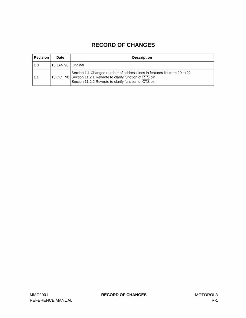
MMC2001 RECORD OF CHANGES MOTOROLA REFERENCE MANUAL R-1
RECORD OF CHANGES
Revision Date Description
1.0 15 JAN 98 Original
1.1 15 OCT 98Section 1.1 Changed number of address lines in features list from 20 to 22Section 11.2.1 Rewrote to clarify function of RTS pinSection 11.2.2 Rewrote to clarify function of CTS pin

MOTOROLA RECORD OF CHANGES MMC2001 R-2 REFERENCE MANUAL
This manual is a product of the Motorola M•Core Technology Center Design Documentation team. Technical writing,illustration, and production editing performed with Adobe® FrameMaker® running on multiple platforms. Cover graphicdesign by Bazzirk, Inc. of Austin, Texas. Printed by Imperial Lithographics, Phoenix, Arizona.