ltr-x130p product data sheet optical sensor
TRANSCRIPT

LITE-ON DCC
RELEASE
BNS-OD-FC001/A4
LITE-ON Technology Corp. / OptoelectronicsNo.90,Chien 1 Road, Chung Ho, New Taipei City 23585, Taiwan, R.O.C.
Tel: 886-2-2222-6181 Fax: 886-2-2221-1948 / 886-2-2221-0660http://www.liteon.com/opto
Optical SensorProduct Data SheetLTR-X130P
Spec No. :DS86-2020-0021Effective Date: 10/22/2020Revision: -

1/30 Part No. : LTR-X130P
BNS-OD-FC002/A4
Optical Sensor LTR-X130P
1. Description
The LTR-X130P is an integrated low voltage I2C proximity sensor (PS), with built-in emitter in a single miniature chipled
lead-free surface mount package.
The PS offers a feature to detect object at user configurable distance up to 10cm, it also provides excellent ambient light
suppression under 100k lux direct sunlight. The sensor has a programmable interrupt with hysteresis to response to events
and that removes the need to poll the sensor for a reading which improves system efficiency. This CMOS design and
factory-set one time trimming capability ensure minimal sensor-to-sensor variations for ease of manufacturability to the end
customers.
2. Features • I2C interface (Standard mode @100kHz or Fast mode @400kHz)
• Ambient Light and Proximity Sensing in one ultra-small ChipLED package
• Very low power consumption with sleep mode capability suited for battery operated devices
• Operating voltage ranges: 1.7V to 3.6V
• Operating temperature ranges: -40 to +85 ºC
• Built-in temperature compensation circuit
• Programmable interrupt function for PS with adjustable upper and lower thresholds
• RoHS and Halogen free compliant
• Fast Response Time
PS Features
Built-in LED driver and detector
High ambient light suppression
8 , 9, 10, 11-bit(selectable) effective resolution
Cancellation of crosstalk
Programmable LED drive settings
Programmable Interrupt
3. Applications • Control brightness of display panel
• Object detection in mobile, computing, and consumer devices.
2/30 Part No. : LTR-X130P
BNS-OD-FC002/A4
Optical Sensor LTR-X130P
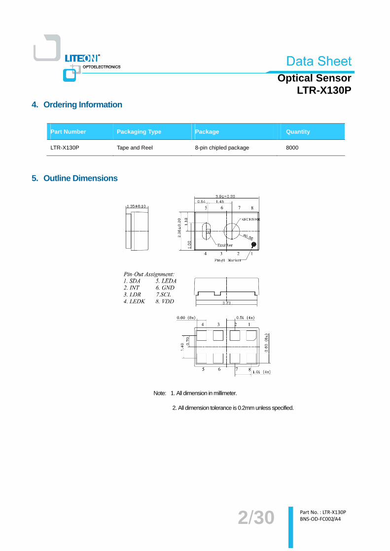
4. Ordering Information
Part Number Packaging Type Package Quantity
LTR-X130P Tape and Reel 8-pin chipled package 8000
5. Outline Dimensions
Note: 1. All dimension in millimeter.
2. All dimension tolerance is 0.2mm unless specified.

3/30 Part No. : LTR-X130P
BNS-OD-FC002/A4
Optical Sensor LTR-X130P
6. Functional Block Diagram
LTR-X130P contains 2 photodiodes (Visible and IR diode) for respective photocurrent measurement. The photodiode currents
are converted to digital values by ADCs. The sensor also included an emitter LED, as well as some peripheral circuits such as
an internal oscillator, a current source, voltage reference, and internal fuses to store trimming information.

4/30 Part No. : LTR-X130P
BNS-OD-FC002/A4
Optical Sensor LTR-X130P
7. Application Circuit
Note: It is a must that VDD and VLED to be separated.
I/O Pins Configuration Table
Pin I/O Type Symbol Description
1 IN/OUT SDA I2C serial data
2 OUT INT Interrupt
3 OUT LDR Connect to LED Cathode
4 OUT LEDK LED Cathode. Connect to LDR pin if internal LED driver circuit is used
5 IN LEDA LED Anode.
6 Ground GND Ground
7 IN SCL I2C serial clock
8 Supply VDD Power Supply Voltage
Recommended Application Circuit Components
Component Recommended Value
Rp1, Rp2, Rp3 [1] 1 kΩ to 10 kΩ
C1, C3 1uF ±20%, X7R / X5R Ceramic
C2 0.1uF
[1] Selection of pull-up resistors value is dependent on bus capacitance values. For more details, please refer to I2C Specifications:
http://www.nxp.com/documents/user_manual/UM10204.pdf

5/30 Part No. : LTR-X130P
BNS-OD-FC002/A4
Optical Sensor LTR-X130P
8. Ratings and Specifications Absolute Maximum Ratings at Ta = 25°°°°C
Parameter Symbol Min. Max Unit
Supply Voltage VDD 4.0 V
Digital Voltage Range SCL, SDA, INT -0.5 4.0 V
Max Voltage Range LDR -0.5 4.0 V
Storage Temperature Tstg -40 100 °C
Electrostatic Discharge Protection
(Human Body Model JESD22-A114) VHBM 2000 V
Note: Exceeding these ratings could cause damage to the sensor. All voltages are with respect to ground. Currents are positive into, negative out of the specified terminal.
Recommended Operating Conditions
Description Symbol Min. Typ. Max. Unit
Supply Voltage VDD 1.7 3.6 V
LED Supply Voltage VLED 3 4.5 V
Interface signal input high VI2Chigh 1.5 VDD V
Interface signal input low VI2Clow 0 0.4 V
Operating Temperature Tope -40 85 °C
Electrical & Optical Specifications
All specifications are at VDD = 2.8V, Tope = 25°C, unless otherwise noted.
Parameter Min. Typ. Max. Unit Condition
Supply Current 95 uA Max. duty cycle, Vdd=2.8V
Standby Current 1 uA Shutdown Mode
Wakeup Time from Standby 5 10 ms From Standby to Active mode
where measurement can start

6/30 Part No. : LTR-X130P
BNS-OD-FC002/A4
Optical Sensor LTR-X130P
Characteristics Proximity Sensor
Parameter Min. Typ. Max. Unit Condition
PS Resolution 8 11 Bit
Sensitivity Range 940 nm
Detection Distance 10 cm No window, 32 pulses, 60kHz, 100mA, 18% Gray Card
LED Pulse Current 2.5 125 mA Configurable for 2.5,5,10,25,50,75,100 & 125mA
LED Pulse Frequency 60 100 kHz
LED Duty Cycle 50 %
Number of LED Pulses 1 255 Pulses
Ambient Light Suppression 100 klux Direct sunlight
Typical Device Parameter
(VDD = 2.8V, Ta=25°C, Default power-up settings, un less otherwise noted)
PS response
Figure 4.1 PS count Vs distance
Angular of LED
Figure 4.2 Emitter Angular of incidence

7/30 Part No. : LTR-X130P
BNS-OD-FC002/A4
Optical Sensor LTR-X130P
AC Electrical Characteristics
All specifications are at VBus = 1.7V, Tope = 25°C, unless otherwise noted.
Parameter Symbol Min. Max. Unit
SCL clock frequency SCLf 1 400 kHz
Bus free time between a STOP and START condition BUFt 1.3 us
Hold time (repeated) START condition. After this period, the first clock pulse is generated STAHDt ; 0.6 us
LOW period of the SCL clock LOWt 1.3 us
HIGH period of the SCL clock HIGHt 0.6 us
Set-up time for a repeated START condition STASUt ; 0.6 us
Set-up time for STOP condition STOSUt ; 0.6 us
Rise time of both SDA and SCL signals rt -- 300 ns
Fall time of both SDA and SCL signals ft -- 300 ns
Data hold time DATHDt ; 0 us
Data setup time DATSUt ; 100 ns
Pulse width of spikes which must be suppressed by the input filter SPt 0 50 ns
Definition of timing for I2C bus

8/30 Part No. : LTR-X130P
BNS-OD-FC002/A4
Optical Sensor LTR-X130P
9. Principles of Operation
I2C Protocols
....I2C Write Protocol (type 1):
....I2C Write Protocol (type 2):
....I2C Read Protocol:
9/30 Part No. : LTR-X130P
BNS-OD-FC002/A4
Optical Sensor LTR-X130P
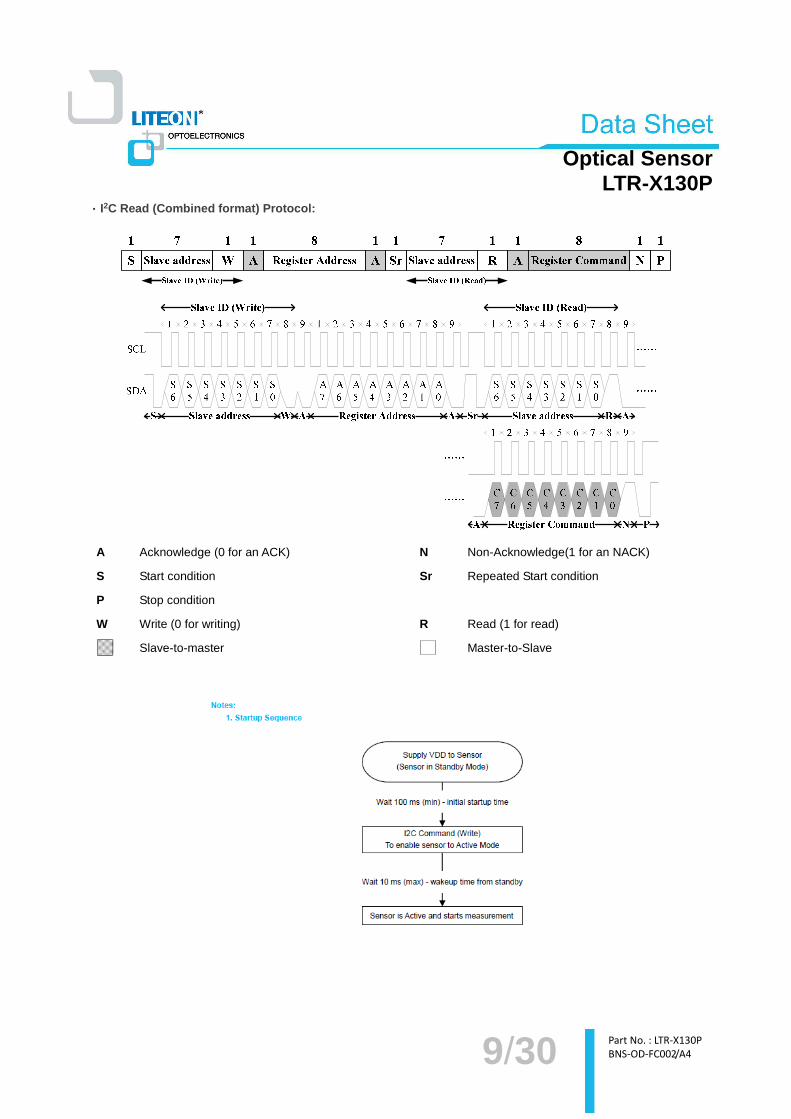
....I2C Read (Combined format) Protocol:
A Acknowledge (0 for an ACK) N Non-Acknowledge(1 for an NACK)
S Start condition Sr Repeated Start condition
P Stop condition
W Write (0 for writing) R Read (1 for read)
Slave-to-master Master-to-Slave

10/30 Part No. : LTR-X130P
BNS-OD-FC002/A4
Optical Sensor LTR-X130P
I2C Slave Address
The 7 bits slave address for this sensor is 0x53H. A read/write bit should be appended to the slave address by the master device
to properly communicate with the sensor.
I2C Slave Address
Command Type
(0x53H) W/R value
Bit7 Bit6 Bit5 Bit4 Bit3 Bit2 Bit1 Bit0
Write 1 0 1 0 0 1 1 0 0xA6H
Read 1 0 1 0 0 1 1 1 0xA7H
Register Set
Addr R / W Register Name Description Reset Value
0x00 RW MAIN_CTRL PS operation mode control, SW reset 0x00
0x01 R/W PS_ LED PS LED settings 0x36
0x02 R/W PS_PULSES PS number of LED pulses 0x08
0x03 R/W PS_MEAS_RATE PS measurement rate in active mode 0x45
0x06 R PART_ID Part number ID and revision ID 0xB1
0x07 R MAIN_STATUS Power-On status, Interrupt status, Data status 0x20
0x08 R PS_DATA_0 PS measurement data, least significant bits 0x00
0x09 R PS_DATA_1 PS measurement data, most significant bits, and overflow 0x00
0x19 R/W INT_CFG Interrupt configuration 0x10
0x1A R/W INT_PST Interrupt persist setting 0x00
0x1B R/W PS_THRES_UP_0 PS interrupt upper threshold, LSB 0xFF
0x1C R/W PS_THRES_UP_1 PS interrupt upper threshold, MSB 0x07
0x1D R/W PS_THRES_LOW_0 PS interrupt lower threshold, LSB 0x00
0x1E R/W PS_THRES_LOW_1 PS interrupt lower threshold, MSB 0x00
0x1F R/W PS_CAN_0 PS intelligent cancellation level setting, LSB 0x00
0x20 R/W PS_CAN_1 PS intelligent cancellation level setting, MSB 0x00

11/30 Part No. : LTR-X130P
BNS-OD-FC002/A4
Optical Sensor LTR-X130P
MAIN_CTRL Register (0x00) (Read/Write)
This register controls the operation modes of PS, which can be set to either standby or active mode. When writing to this
register, it will cause a stop to any ongoing measurements and start new measurement.
0x00 MAIN_CTRL (default = 0x00)
B7 B6 B5 B4 B3 B2 B1 B0
Reserved Software
Reset Reserved PS Enable
Field Bits Default Description
Reserved 7:5 000 -- --
SW Reset 4 0 0 Software reset is NOT triggered (default)
1 Software reset is triggered
Reserved 3:1 00 -- --
PS Enable 0 0 0 PS standby(default)
1 PS active
PS_LED Register (0x01) (Read/Write)
This register controls the LED driving current and the LED pulse modulation frequency.
0x01 PS_LED (default = 0x36)
B7 B6 B5 B4 B3 B2 B1 B0
Reserved LED Pulse Modulation Frequency Reserved LED Current
Field Bits Default Description
Reserved 7 0 - -
LED pulse 4:6 011 000 Reserved

12/30 Part No. : LTR-X130P
BNS-OD-FC002/A4
Optical Sensor LTR-X130P
modulation
Frequency
001 Reserved
010 Reserved
011 LED pulse period = 60kHz(default)
100 LED pulse period = 70kHz
101 LED pulse period = 80kHz
110 LED pulse period = 90kHz
111 LED pulse period = 100kHz
Reserved 3 0 - -
LED current 2:0 110
000 LED pulsed current level = 2.5mA
001 LED pulsed current level = 5.0mA
010 LED pulsed current level = 10mA
011 LED pulsed current level = 25mA
100 LED pulsed current level = 50mA
101 LED pulsed current level = 75mA
110 LED pulsed current level = 100mA (default)
111 LED pulsed current level = 125mA
PS_PULSES Register (0x02) (Read/Write)
This register controls number of PS LED pulses emitted.
0x02 PS_PULSES (default = 0x08)
B7 B6 B5 B4 B3 B2 B1 B0
Number of LED Pulses
Field Bits Default Description
Number of
LED
pulses
7:0 0000 1000
00 0000 0 pulse (no light emission)
00 0001 1 pulse
00 0010 2 pulses
… …

13/30 Part No. : LTR-X130P
BNS-OD-FC002/A4
Optical Sensor LTR-X130P
00 1000 8 pulses (default)
… …
10 0000 32 pulses
1111 1111 255 pulses
PS_MEAS_RATE Register (0x03) (Read/Write)
This register controls the timing of the periodic measurements of the PS during active mode. When the measurement
rate is programmed to be faster than possible for the programmed ADC measurement, the rate will be lowered than
programmed (maximum speed).
0x03 PS_MEAS_RATE (default = 0x45)
B7 B6 B5 B4 B3 B2 B1 B0
0 1 0 PS Resolution/Bit
Width PS Measurement Rate
Field Bits Default Description
Reserved 7:5 010 Must write 010
PS
Resolution/Bit
Width
4:3 00
00 8 bit(default)
01 9 bit
10 10 bit
11 11 bit
PS
Measurement
Rate
2:0 101
000 Reserved
001 6.25ms
010 12.5ms
011 25 ms
100 50ms
101 100ms(default)
110 200ms
111 400ms

14/30 Part No. : LTR-X130P
BNS-OD-FC002/A4
Optical Sensor LTR-X130P
PART_ID Register (0x06) (Read Only)
This register defines the part number and revision identification of the sensor.
0x06 PART_ID (default = 0xB1)
B7 B6 B5 B4 B3 B2 B1 B0
Part Number ID Revision ID
Field Bits Default Description
Part Number ID 7:4 1011 Part Number ID
Revision ID 3:0 0001 Revision ID
MAIN_STATUS Register (0x07) (Read Only)
This register stores the information about the PS interrupts and data status. The interrupt status in Bit 1 determines if
the PS interrupt criteria are met in Normal Interrupt Mode. It triggers when the PS data is above the upper or below the
lower threshold for a specified number of consecutive measurements in respective interrupt persist settings. This
register also provides PS logic signal status, which is used for indicating whether the detected object is near (PS data
larger than PS upper threshold settings) or far (PS data smaller than PS lower threshold settings). For details interrupt
behavior, refer to Section 10.
0x07 MAIN_STATUS (default = 0x20)
B7 B6 B5 B4 B3 B2 B1 B0
Reserved Power ON
Status Reserved
PS Logic Signal Status
PS Interrupt Status
PS Data Status
Field Bits Default Description
Reserved 7:6 00 -- --

15/30 Part No. : LTR-X130P
BNS-OD-FC002/A4
Optical Sensor LTR-X130P
Power On
Status 5 0 0
Power on event and All interrupt threshold settings in the registers
have been rest to power on default states (either due to part turned
on or power supply voltage glitch). Flag is cleared after read.
Reserved 4:3 00 -- --
PS Logic
Signal
Status
2 0
0 Object is far (default)
1 Object is near
PS Interrupt Status
1 0 0 Interrupt is NOT triggered (default)
1 Interrupt is triggered and will be cleared after read
PS Data
Status 0 0
0 PS data is old data (Data has been read)
1 PS data is new data (Data has not been read and will be cleared
after read)
PS_DATA Register (0x08 / 0x09) (Read Only)
The PS ADC channel data are expressed as an 11-bit data spread over 2 registers. The PS_DATA_0 and PS_DATA_1
registers provide the lower and upper byte respectively. An overflow bit is available to check if the PS data overflows.
When I2C read operation is active and points to any of the register address between 0x07 and 0x18, both registers
PS_DATA_0 and PS_DATA_1 will be locked until the I2C read operation has been completed or the specified address
range is left. New measurement data is stored into temporary registers and the PS_DATA registers will be updated as
soon as there is no on-going I2C read operation to the address range 0x07 to 0x18.
0x08 PS_DATA_0 (default = 0x00)
B7 B6 B5 B4 B3 B2 B1 B0
PS Data Low
0x09 PS_DATA_1 (default = 0x00)
B7 B6 B5 B4 B3 B2 B1 B0
Reserved Overflow PS Data High

16/30 Part No. : LTR-X130P
BNS-OD-FC002/A4
Optical Sensor LTR-X130P
Field Address Bits Default Description
PS Data,
Low 0x08 7:0 00000000 -- PS ADC lower byte data
Reserved 0x09 7:4 000 -- --
Overflow 0x09 3 0 0 Valid PS data (default)
1 Overflow of PS data
PS Data,
High 0x09 2:0 000 -- PS ADC upper byte data
INT_CFG Register (0x19) (Read/Write)
This register controls the operation of the interrupt pin and functions. PS have independent interrupt signal it is active low.
PS interrupt is enabled by Bit 0, and it is threshold triggered based. Besides, Under Normal Interrupt Mode, the
edge-triggered interrupt signal output will be maintains at active level until MAIN_STATUS register is read. While for PS
Logic Output Mode, the interrupt pin output is updated after every measurement and output state is maintained between
measurements.
0x19 INT_CFG (default = 0x10)
B7 B6 B5 B4 B3 B2 B1 B0
Reserved PS
OUTPUT MODE
PS INT PIN
ENABLE
Field Bits Default Description
Reserved 7:2 00 -- --
PS OUTPUT
MODE 1 0
0 Normal Interrupt Mode: After interrupt event, INT output pin
maintains active level until MAIN_STATUS register is read (default)
1 PS Logic Output Mode: INT output pin is updated after every
measurement and maintains output state between measurements.
PS Interrupt
Pin Enable 0 0
0 PS interrupt enabled (default)
1 PS interrupt enabled
17/30 Part No. : LTR-X130P
BNS-OD-FC002/A4
Optical Sensor LTR-X130P
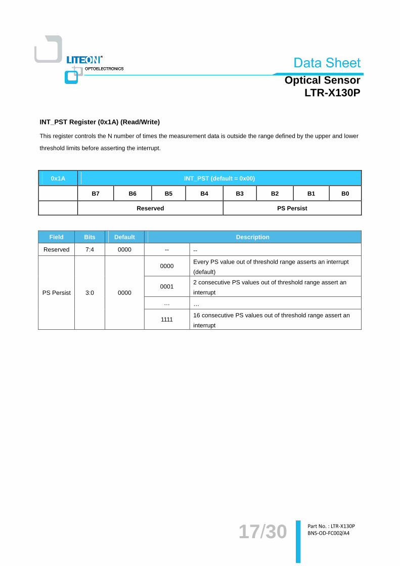
INT_PST Register (0x1A) (Read/Write)
This register controls the N number of times the measurement data is outside the range defined by the upper and lower
threshold limits before asserting the interrupt.
0x1A INT_PST (default = 0x00)
B7 B6 B5 B4 B3 B2 B1 B0
Reserved PS Persist
Field Bits Default Description
Reserved 7:4 0000 -- --
PS Persist 3:0 0000
0000 Every PS value out of threshold range asserts an interrupt
(default)
0001 2 consecutive PS values out of threshold range assert an
interrupt
… …
1111 16 consecutive PS values out of threshold range assert an
interrupt

18/30 Part No. : LTR-X130P
BNS-OD-FC002/A4
Optical Sensor LTR-X130P
PS_THRES Register (0x1B / 0x1C / 0x1D / 0x1E) (Read/Write)
The PS_THRES_UP and PS_THRES_LOW registers determines the upper and lower limit of the interrupt threshold value
respectively. Interrupt will be triggered if measurement data in PS_DATA registers is exceeding the upper and lower limits.
0x1B PS_THRES_UP_0 (default = 0xFF)
B7 B6 B5 B4 B3 B2 B1 B0
PS Upper Threshold, Low
0x1C PS_THRES_UP_1 (default = 0x07)
B7 B6 B5 B4 B3 B2 B1 B0
Reserved PS Upper Threshold, High
0x1D PS_THRES_LOW_0 (default = 0x00)
B7 B6 B5 B4 B3 B2 B1 B0
PS Lower Threshold, Low
0x1E PS_THRES_LOW_1 (default = 0x00)
B7 B6 B5 B4 B3 B2 B1 B0
Reserved PS Lower Threshold, High
Field Address Bits Default Description
PS Upper Threshold, Low
0x1B 7:0 11111111 PS Upper Interrupt Threshold, Low byte
Reserved 0x1C 7:3 00000 --
PS Upper Threshold, High
0x1C 2:0 111 PS Upper Interrupt Threshold, High byte
PS Lower Threshold, Low
0x1D 7:0 00000000 PS Lower Interrupt Threshold, Low byte
Reserved 0x1E 7:3 00000 --
PS Lower Threshold, High
0x1E 2:0 000 PS Lower Interrupt Threshold, High byte

19/30 Part No. : LTR-X130P
BNS-OD-FC002/A4
Optical Sensor LTR-X130P
PS_CAN Register (0x1F / 0x20) (Read/Write)
This register defines the offset compensation value for proximity offsets caused by device variations, optical crosstalk and
other environment factors. This register sets the PS cancellation value to be subtracted from the measured PS data before
the data is transferred to the PS_DATA registers.
0x1F PS_CAN_0 (default = 0x00)
B7 B6 B5 B4 B3 B2 B1 B0
PS Cancellation Level, Low
0x20 PS_CAN_1 (default = 0x00)
B7 B6 B5 B4 B3 B2 B1 B0
Reserved PS Cancellation Level, High
Field Address Bits Default Description
PS Cancellation
Level, Low 0x1F 7:0 00000000 PS Cancellation Level, Low byte
Reserved 0x20 7:3 00000 --
PS Cancellation
Level, High 0x20 2:0 000 PS Cancellation Level, High byte

20/30 Part No. : LTR-X130P
BNS-OD-FC002/A4
Optical Sensor LTR-X130P
10. Application Information
10.1 Device Operation (State Machine and Interrupt Features)
State Machine
Below diagram is the main state machine of LTR-X130P.
During the PS Operation, PS measurement can be activated by setting the PS_Enable bit to 1. As soon as the PS
sensors become activated through an I2C command, the internal support blocks are powered on. Once the voltages and
currents are settled (typically after 5ms), the state machine checks for trigger events from a measurement scheduler to
start PS conversions according to the selected measurement repeat rates. Once PS_Enable is changed back to 0, a
running conversion on the respective channel will be completed and the relevant ADCs and support blocks will move to
power-down state.

21/30 Part No. : LTR-X130P
BNS-OD-FC002/A4
Optical Sensor LTR-X130P
PS Interrupt
The PS interrupt is enabled by Bit 0 (PS Interrupt Pin Enable). It triggers when the PS conversion result is above
the upper or below PS threshold for a specified number of consecutive measurements set in PS Persist in
INT_PST register (0x1A). The PS Logic Signal, Bit 2 of MAIN_STATUS register (0x07), is set to 0 when the PS
data is below the lower PS threshold and it set to 1 if the PS data is above the upper PS threshold.
There are two options to indicate a PS interrupt signal on the INT pin: as a continuous logic signal or as an
edge-triggered interrupt signal, which is cleared with the next read-out of the MAIN-STATUS register. The PS
interrupt signal is also stored in MAIN_STATUS register (0x07) as flag bit in Bit 1 (PS INT Status). This status flag
bit is cleared by reading the MAIN_STATUS register. The PS interrupt behavior is as shown below.

22/30 Part No. : LTR-X130P
BNS-OD-FC002/A4
Optical Sensor LTR-X130P
11. Pseudo Codes Examples
Slave address
Slave_Addr = 0xA6
MAIN_CTRL Register
// This defines the operating modes of the PS // Default settings is 0x00 (PS standby) Register_Addr = 0x00 // MAIN_CTRL register Command = 0x01 // PS in Active Mode, WriteByte(Slave_Addr, Register_Addr, Command);
PS_LED Register
// This defines the LED pulse modulation frequency and Peak current. // Default setting is 0x36 (Pulse Freq = 60kHz, peak current = 100mA). Register_Addr = 0x01 // PS_LED register Command = 0x36 // Pulse Freq = 60kHz, Peak Current =100mA // Command = 0x46 Pulse Freq = 70kHz, Peak Current =100mA
// Command = 0x44 Pulse Freq = 70kHz, Peak Current = 50mA // Command = 0x76 Pulse Freq = 100kHz, Peak Current = 100mA // Command = 0x77 Pulse Freq = 100kHz, Peak Current = 125mA
WriteByte(Slave_Addr, Register_Addr, Command)
PS_PULSES Register
// This controls the number of PS LED pulses emitted. // Default setting of the register is 0x08 (8 Pulses) Register_Addr = 0x02 // PS_PULSES register Command = 0x08 // 8 pulses // Command = 0x00 0 (no light) // Command = 0x04 4 pulses // Command = 0x20 32 pulses WriteByte(Slave_Addr, Register_Addr, Command)
PS_MEAS_RATE Register
//This controls the PS Resolution and measurement rate. // Default setting of the register is 0x45 (PS Resolution = 8 bit, Measurement Rate = 100ms) Register_Addr = 0x03 // PS_MEAS_RATE register Command = 0x45 // Resolution = 8 bit, Meas Rate = 100ms
// Command = 0x47 Resolution = 8 bit Meas Rate = 400ms // Command = 0x5D Resolution = 11 bit Meas Rate = 100ms WriteByte(Slave_Addr, Register_Addr, Command)

23/30 Part No. : LTR-X130P
BNS-OD-FC002/A4
Optical Sensor LTR-X130P
MAIN_STATUS Register (Read Only)
// This Register contains the information on Interrupt, PS data status. Register_Addr = 0x07 // MAIN_STATUS register address Data = ReadByte(Slave_Addr, Register_Addr) Power_ON_Status = Data & 0x20 // If 0x20 Part went through power-up event // If 0x00 Normal PS_Logic_Signal_Status = Data & 0x04 // If 0x04 Object is near // If 0x00 Object is far PS_Interrupt_Status = Data & 0x02 // If 0x02 Interrupt triggered // If 0x00 Interrupt condition not fulfilled PS_Data_Status = Data & 0x01 // If 0x01 PS data is new // If 0x00 Old (previously read) Data
PS_DATA Registers (Read Only)
//The register 0x08 contains PS ADC lower byte data. //The register 0x09 contains PS ADC 3 bits of upper byte data and PS Overflow flag //These registers should be read as a group, with the lower address being read first. Register_Addr = 0x08 // PS_DATA0 low byte address Data0=ReadByte(Slave_Addr, Register_Addr) // Data= PS ADC lower byte data Register_Addr = 0x09 // PS_DATA1 high byte address Data=ReadByte(Slave_Addr, Register_Addr) // Data= PS ADC high byte data Data1=Data&0x03 // Mask with 0x03 to extract data PS_ADC_Data = (Data1 << 8) | Data0 // Shift and combine lower and upper bytes to give 11-bit PS data Overflow_status = Data & 0x08 // If 0x08 PS Data is overflow // If 0x00 PS Data is valid
CLEAR_DATA Registers (Read Only)
//The register 0x0A contains CLEAR_DATA ADC 0 lower byte data. //The register 0x0B contains CLEAR_DATA ADC 1 middle byte data. //The register 0x0C contains CLEAR_DATA ADC 2 upper byte data. //These registers should be read as a group, with the lower address being read first. Register_Addr = 0x0A // CLEAR_DATA_0 low byte address Data0=ReadByte(Slave_Addr, Register_Addr) Register_Addr = 0x0B // CLEAR_DATA_1 middle byte address Data1=ReadByte(Slave_Addr, Register_Addr) Register_Addr = 0x0C // CLEAR_DATA_2 upper byte address Data2=ReadByte(Slave_Addr, Register_Addr) CLEAR_Data =(Data2<<16)| (Data1 << 8) | Data0 // Shift and combine all register data to get CLEAR ADC Data
INT_CFG Register
//This register controls the operation of the interrupt pins and options to trigger interrupt for PS. //The default value for this INT_CFG register is 0x10 (Interrupts inactive for both PS) Register_Addr = 0x19 // INT_CFG Register address Command = 0x15 // Interrupt Enable // Command = 0x17 // PS Logic Output Mode; PS Interrupt Enable

24/30 Part No. : LTR-X130P
BNS-OD-FC002/A4
Optical Sensor LTR-X130P
// Command = 0x05 // Normal Trigger Mode; PS Interrupt Enable // Command = 0x14 // Normal Trigger Mode; PS Interrupt Disable // Command = 0x11 // Normal Trigger Mode; PS Interrupt Enable WriteByte(Slave_Addr, Register_Addr, Command)
INTERRUPT_PERSIST Register
// This register sets the PS persist level. // The default setting is 0x00. Interrupt at every PS reading outside set thresholds. Register_Addr = 0x1A // INT_PST register Command = 0x00 // Interrupt for every PS value outside threshold // Command =0x10 Subsequent every PS value, outside threshold range // Command =0x11 Subsequent 2 PS values, outside threshold range // Command =0x35 Subsequent 6 PS values, outside threshold range WriteByte(Slave_Addr, Register_Addr, Command)
PS_THRES Registers
// The register 0x1B contains PS Interrupt upper threshold lower byte data (PS_THRES_UP_0) // The register 0x1C contains PS Interrupt upper threshold upper byte data (PS_THRES_UP_1) // The register 0x1D contains PS Interrupt lower threshold lower byte data (PS_THRES_LOW_0) // The register 0x1E contains PS Interrupt lower threshold upper byte data (PS_THREH_LOW_1) // To set PS Upper threshold for Interrupt Upper_Threshold_Value=1000 // Example 1000 Data1 = Upper_Threshold_Value >> 8 // Shift right to extract the upper byte Data0 = Upper_Threshold_Value & 0xFF // Mask to extract lower byte. Register_Addr = 0x1B // PS_THRES_UP_0 Register address WriteByte(Slave_Addr, Register_Addr, Data0) Register_Addr = 0x1C // PS_THRES_UP_1 Register address WriteByte(Slave_Addr, Register_Addr, Data1) // To set PS Lower threshold for Interrupt Lower_Threshold_Value=100 // Example 100 Data1 = Lower_Threshold_Value >> 8 // Shift right to extract the upper byte Data0 =Lower_Threshold_Value & 0xFF // Mask to extract lower byte. Register_Addr = 0x1D // PS_THRES_LOW_0 Register address WriteByte(Slave_Addr, Register_Addr, Data0) Register_Addr = 0x1E // PS_THRES_LOW_1 Register address WriteByte(Slave_Addr, Register_Addr, Data1)
PS_CAN Registers
//The register 0x1F contains PS cancellation lower byte data (PS_CAN_0) //The register 0x20 contains 3 bits of PS cancellation upper byte data (PS_CAN_1) //To set PS Cancellation Value (0 to 2047) PS_Cancel_Value=100 // Example 100 Data1 = PS_Cancel_Value >> 8 // Shift right to extract the upper byte Data0 = PS_Cancel_Value & 0xFF // Mask to extract lower byte. Register_Addr = 0x1F // PS_CAN_0 Register address WriteByte(Slave_Addr, Register_Addr, Data0) Register_Addr = 0x20 // PS_CAN_1 Register address WriteByte(Slave_Addr, Register_Addr, Data1)

25/30 Part No. : LTR-X130P
BNS-OD-FC002/A4
Optical Sensor LTR-X130P
12. Recommended Leadfree Reflow Profile
50 100 150 200 250 300t-TIME(SECONDS)
25
80
120
150
180200
230
255
0
T -
TE
MP
ER
AT
UR
E (
°C)
R1
R2
R3 R4
R5
217
MAX 260C
60 sec to 90 secAbove 217 C
P1HEAT UP
P2SOLDER PASTE DRY
P3SOLDERREFLOW
P4COOL DOWN
Process Zone Symbol ∆∆∆∆T Maximum ∆∆∆∆T/∆∆∆∆time or Duration
Heat Up P1, R1 25°C to 150°C 3°C/s
Solder Paste Dry P2, R2 150°C to 200°C 100s to 180s
Solder Reflow P3, R3
P3, R4
200°C to 260°C
260°C to 200°C
3°C/s
-6°C/s
Cool Down P4, R5 200°C to 25°C -6°C/s
Time maintained above liquidus point , 217°C > 217°C 60s to 90s
Peak Temperature 260°C -
Time within 5°C of actual Peak Temperature > 255°C 20s
Time 25°C to Peak Temperature 25°C to 260°C 8mins
It is recommended to perform reflow soldering no more than twice.
26/30 Part No. : LTR-X130P
BNS-OD-FC002/A4
Optical Sensor LTR-X130P
13. Moisture Proof Packaging
All LTR-X130P are shipped in moisture proof package. Once opened, moisture absorption begins. This part is compliant
to JEDEC J-STD-033A Level 3.
Time from Unsealing to Soldering
After removal from the moisture barrier bag, the parts should be stored at the recommended storage conditions and
soldered within seven days. When the moisture barrier bag is opened and the parts are exposed to the recommended
storage conditions for more than seven days, the parts must be baked before reflow to prevent damage to the parts.
Recommended Storage Conditions
Storage Temperature 10°C to 30°C
Relative Humidity Below 60% RH
Baking Conditions
Package Temperature Time
In Reels 60°C 48 hours
In Bulk 100°C 4 hours
Baking should only be done once.

27/30 Part No. : LTR-X130P
BNS-OD-FC002/A4
Optical Sensor LTR-X130P
14. Recommended Land Pattern and Metal Stencil Aperture
Recommended Land Pattern
Note: All dimensions are in millimeters
Metal Stencil
for Solder
Paste Printing
Stencil
Apertur
e
Land
Pattern
PCB

28/30 Part No. : LTR-X130P
BNS-OD-FC002/A4
Optical Sensor LTR-X130P
Recommended Metal Stencil Aperture
It is recommended that the metal stencil used for solder paste printing has a thickness (t) of 0.11mm (0.004 inches / 4 mils)
or 0.127mm (0.005 inches / 5 mils).
The stencil aperture opening is recommended to be 0.75mm x 0.75mm which has the same dimension as the land pattern.
This is to ensure adequate printed solder paste volume and yet no shorting.
2.15
3.78
t
Aperture
Opening

29/30 Part No. : LTR-X130P
BNS-OD-FC002/A4
Optical Sensor LTR-X130P
15. Package Dimension for Tape and Reel
Notes: 1. All dimensions are in millimeters 2. Empty component pockets sealed with top cover tape 3. 13 inch reel - 8000 pieces per reel 4. In accordance with ANSI/EIA 481-1-A-1994 specifications
User direction of unreeling

30/30 Part No. : LTR-X130P
BNS-OD-FC002/A4
Optical Sensor LTR-X130P
Revision Table:
Version Update Page Date
1.0 Datasheet as created Total 30 28-02-2020