ltm4641 - 38v, 10a dc/dc μmodule regulator with advanced ... · l4641 4641 for more information
TRANSCRIPT

LTM4641
14641fe
For more information www.linear.com/LTM4641
Typical applicaTion
FeaTures DescripTion
38V, 10A DC/DC µModule Regulator with Advanced Input and Load Protection
The LTM®4641 is a switch mode step-down DC/DC µModule® (micromodule) regulator with advanced input and load protection features. Trip detection thresholds for the following faults are customizable: input undervoltage, overtemperature, input overvoltage and output overvolt-age. Select fault conditions can be set for latchoff or hysteretic restart response—or disabled. Included in the package are the switching controller and housekeeping ICs, power MOSFETs, inductor, overvoltage drivers, biasing circuitry and supporting components. Operating from input voltages of 4V to 38V (4.5V start-up), the device supports output voltages from 0.6V to 6V, set by an external resis-tor network remote sensing the point-of-load’s voltage.
The LTM4641’s high efficiency design can deliver up to 10A continuous current with a few input and output ca-pacitors. The regulator’s constant on-time current mode control architecture enables high step-down ratios and fast response to transient line and load changes. The LTM4641 is offered in a 15mm × 15mm × 5.01mm with SnPb or RoHS compliant terminal finish.
applicaTions
n Wide Operating Input Voltage Range: 4.5V to 38Vn 10A DC Typical, 12A Peak Output Currentn Output Range: 0.6V to 6Vn ±1.5% Maximum Total Output DC Voltage Errorn Differential Remote Sense Amplifier for POL Regulationn Internal Temperature, Analog Indicator Outputn Overcurrent Foldback and Overtemperature
Protectionn Current Mode Control/Fast Transient Responsen Parallelable for Higher Output Currentn Selectable Pulse-Skipping Operationn Soft-Start/Voltage Tracking/Pre-Bias Start-Upn 15mm × 15mm × 5.01mm BGA Packagen SnPb or RoHS Compliant FinishInput Protectionn UVLO, Overvoltage Shutdown and Latchoff Thresholdsn N-Channel Overvoltage Power-Interrupt MOSFET Drivern Surge Stopper Capable with Few External ComponentsLoad Protectionn Robust, Resettable Latchoff Overvoltage Protectionn N-Channel Overvoltage Crowbar Power MOSFET Driver
n Ruggedized Electronicsn Avionics and Industrial Equipment
L, LT, LTC, LTM, µModule, Burst Mode, Linear Technology and the Linear logo are registered trademarks and LTpowerCAD is a trademark of Linear Technology Corporation. All other trademarks are the property of their respective owners. Protected by U.S. Patents including 5481178, 5847554, 6100678, 6304066, 6580258, 6677210, 8163643.
1V Load Protected from MTOP Short-Circuit at 38VIN
µModule Regulator with Input Disconnect and Fast Crowbar Output Overvoltage Protection
+
IOVRETRY
VING VINGP VINH SW
MCB**
MBOT
MTOP
MSP*
4
3
1
2VOUT
CROWBAR
VOSNS+
VOSNS–
GND
OVPGM
VINL
fSET
750k
5.6M
4641 TA01a
SGND CONNECTS TO GND INTERNAL TO µMODULE REGULATORMSP: (OPTIONAL) SERIES-PASS OVERVOLTAGE POWER INTERRUPT MOSFET, NXP PSMN014-60LSMCB: (OPTIONAL) OUTPUT OVERVOLTAGE CROWBAR MOSFET, NXP PH2625L
***
5.49k
5.49kLTM4641
10µF50V×2
UVLOINTVCCDRVCC
RUN
10nF
TRACK/SS
OVLO FCB LATCH SGND
100µF×3
VOUT1V10A
100µF50V
VIN4V TO 38V
4.5V START-UP
LOAD
Click to view associated TechClip Videos.
VOUT(200mV/DIV)
4µs/DIVTESTED AT WORST-CASE CONDITION: NO LOAD
4641 TA01b
SHORT-CIRCUIT APPLIED
1.1VOUT PEAK
CROWBAR (5V/DIV)
4
32
1
VINL, VINH (25V/DIV)

LTM4641
24641fe
For more information www.linear.com/LTM4641
Table oF conTenTs Features ..................................................... 1Applications ................................................ 1Typical Application ........................................ 1Description.................................................. 1Absolute Maximum Ratings .............................. 3Order Information .......................................... 3Pin Configuration .......................................... 3Electrical Characteristics ................................. 4Typical Performance Characteristics ................... 8Pin Functions .............................................. 10Simplified Block Diagram ............................... 15Decoupling Requirements ............................... 15Operation................................................... 16
Introduction ............................................................ 16Motivation ............................................................... 16Power µModule Regulator Reliability ...................... 16Overview ................................................................. 16
Applications Information—Power Supply Features . 17Power (VINH) and Bias (VINL) Input Pins ................. 17Switching Frequency (On Time) Selection and Voltage Dropout Criteria (Achievable VIN-to-VOUT Step-Down Ratios).................................................. 18Setting the Output Voltage; the Differential Remote Sense Amplifier ......................................... 21Input Capacitors .....................................................23Output Capacitors and Loop Stability/Loop Compensation .........................23Pulse-Skipping Mode vs Forced Continuous Mode ....................................... 24Soft-Start, Rail-Tracking and Start-Up Into Pre-Bias .................................................................. 24INTVCC and DRVCC ............................................................... 271VREF ......................................................................................... 28TEMP, OTBH and Overtemperature Protection ........28Input Monitoring Pins: UVLO, IOVRETRY, OVLO ....29
Applications Information—Input Protection Features .................................................... 29
Start-Up/Shutdown and Run Enable; Power-On Reset and Timeout Delay Time ............... 31
Applications Information—Load Protection Features .................................................... 32
Overcurrent Foldback Protection ............................32Power Good Indicator and Latching Output Overvoltage Protection ...........................................32Power-Interrupt MOSFET (MSP), CROWBAR Pin and Output CROWBAR MOSFET (MCB) ..................33Fast Output Overvoltage Comparator Threshold .....34The Switching Node: SW Pin ..................................35
Applications Information—EMI Performance ........ 35Applications Information—Multimodule Parallel Operation ........................................ 36Applications Information—Thermal Considerations and Output Current Derating ............................ 38
Thermal Considerations and Output Current Derating .........................................38
Applications Information—Output Capacitance Table ........................................................ 45Applications Information—Safety and Layout Guidance ................................................... 46
Safety Considerations .............................................46Layout Checklist/Example ......................................46
Typical Applications ...................................... 48Appendices ................................................ 56
Appendix A. Functional Block Diagram and Features Quick Reference Guide .............................56Appendix B. Start-Up/Shutdown State Diagram .....57Appendix C. Switching Frequency Considerations and Usage of RfSET .................................................58Appendix D. Remote Sensing in Harsh Environments ...............................................59Appendix E. Inspiration For Pulse-Skipping Mode Operation ......................................................60Appendix F. Adjusting the Fast Output Overvoltage Comparator Threshold ............................................60
Package Description ..................................... 63Package Photo ............................................ 63Package Description ..................................... 64Revision History .......................................... 65Typical Application ....................................... 66Related Parts .............................................. 66

LTM4641
34641fe
For more information www.linear.com/LTM4641
pin conFiguraTionabsoluTe MaxiMuM raTings
Terminal Voltages VINL, VINH, SW, fSET ............................... –0.3V to 40V VOUT...................................................... –0.3V to 9.2V VING ............................................ –0.3V to VINH + 20V INTVCC, DRVCC, RUN, TRACK/SS, PGOOD,
CROWBAR, HYST .................................... –0.3V to 6V FCB, TMR................................-0.3V to INTVCC + 0.3V COMP ................................................... –0.3V to 2.7V VOSNS
+, VORB+ ...................................... –0.6V to 9.7V
VOSNS–, VORB
– ..........VOSNS+ – 2.7V to VOSNS
+ + 0.3V OTBH, UVLO, IOVRETRY, OVLO,
LATCH ....................................................–0.3V to 7.5V TEMP, OVPGM ....................................... –0.3V to 1.5VTerminal Currents INTVCC (Continuous)....................................... –30mA INTVCC (Continuous; CROWBAR Sourcing 15mA) ...............................................–15mA CROWBAR (Continuous) ..................................–15mA VINGP (Continuous) ........................... –50mA to 15mA 1VREF (Continuous) ................................–1mA to 1mAInternal Operating Temperature Range (Note 2) E- and I-Grades .................................. –40°C to 125°C MP-Grade .......................................... –55°C to 125°CStorage Temperature Range .................. –55°C to 125°CPeak Package Body Temperature (SMT Reflow) ... 245°C
(Note 1)
SW
BGA PACKAGE144-LEAD (15mm × 15mm × 5.01mm)
TOP VIEW
GND
GND
GND
GND
1 2 3 4 5 6 7 8 109 11 12
L
K
J
H
G
F
E
D
C
B
M
A
OVPGMCROWBARTEMP IOVRETRY
1VREF
OVLOHYSTUVLO
SGND
VORB–
VORB+
VOSNS–
VOSNS+
DRVCC
SGND
VINL
fSET
LATCH
RUNTMROTBH
COMP
PGOODTRACK/SS VINH
VOUT
VINGPVINGSGND INTVCC
FCB
TJMAX = 125°C, θJCtop = 11°C/W, θJCbottom = 2.5°C/W
θJB = 3°C/W, θJA = 10.4°C/W θ VALUES DETERMINED PER JESD51-12
WEIGHT = 2.9 GRAMS
orDer inForMaTionPART NUMBER PAD OR BALL FINISH PART MARKING* PACKAGE
TYPEMSL
RATINGTEMPERATURE RANGE (Note 2)DEVICE FINISH CODE
LTM4641EY#PBF SAC305 (RoHS) LTM4641Y e1 BGA 4 –40°C to 125°CLTM4641IY#PBF SAC305 (RoHS) LTM4641Y e1 BGA 4 –40°C to 125°CLTM4641IY SnPb (63/37) LTM4641Y e0 BGA 4 –40°C to 125°CLTM4641MPY#PBF SAC305 (RoHS) LTM4641Y e1 BGA 4 –55°C to 125°CLTM4641MPY SnPb (63/37) LTM4641Y e0 BGA 4 –55°C to 125°C
Consult Marketing for parts specified with wider operating temperature ranges. *Device temperature grade is indicated by a label on the shipping container. Pad or ball finish code is per IPC/JEDEC J-STD-609.• Pb-free and Non-Pb-free Part Markings:
www.linear.com/leadfree
• Recommended LGA and BGA PCB Assembly and Manufacturing Procedures: www.linear.com/umodule/pcbassembly
• LGA and BGA Package and Tray Drawings: www.linear.com/packaging

LTM4641
44641fe
For more information www.linear.com/LTM4641
elecTrical characTerisTics The l denotes the specifications which apply over the full internal operating temperature range, otherwise specifications are at TA = 25°C (Note 2). VIN = VINH = VINL = 28V, per the typical application shown in Figure 45, unless otherwise noted.
SYMBOL PARAMETER CONDITIONS MIN TYP MAX UNITS
VIN Input DC Voltage l 4.5 38 V
VOUT Output Voltage Range Use RSET1A = RSET1B ≤ 8.2kΩ. RfSET Values Recommended in Table 1
l 0.6 6 V
VOUT(DC) Output Voltage, Total Variation with Line and Load, and Prior to UVLO
4.5V ≤ VIN ≤ 38V, 0A ≤ IOUT ≤ 10A VIN = 4V (Ramped Down from 4.5V), IOUT = 0A
l
l
1.773 1.773
1.800 1.800
1.827 1.827
V V
Input Specifications
VRUN(ON,OFF) RUN On/Off Threshold Run Rising, Turn On Run Falling, Turn Off
l
l
0.8
1.25 1.15
2 V V
IRUN(ON) RUN Pull-Up Current VRUN = 0V VRUN = 3.3V
l
l
–580 –220
–520 –165
–460 –110
µA µA
IRUN(OFF) RUN Pull-Down Current, Switching Inhibited
VRUN = 3.3V, UVLO = 0V (MHYST On) 1 nA
VINL(UVLO) VINL Undervoltage Lockout VINL Rising VINL Falling Hysteresis
l
l
l
3.5 300
4.2 3.8 400
4.5 4
V V
mV
IINRUSH(VINH) Input Inrush Current Through VINH, at Start-Up
CSS = Open 230 mA
IQ(VINH) Power Stage Bias Current (IVINH) at No Load
IOUT = 0A and: FCB ≥ 0.84V (Pulse-Skipping Mode) FCB ≤ 0.76V (Forced Continuous Mode) Shutdown, RUN = 0
8
29 0.2
mA mA mA
IQ(VINL) Control Bias Current (IVINL) INTVCC Connected to DRVCC and: VIN = 28V, IOUT = 0A VIN = 28V, IOUT = 10A VIN = 28V, Shutdown, RUN = 0
14.5 15.5
5
mA mA mA
IS(VINH) Power Stage Input Current (IVINH) at Full Load
IOUT = 10A and: VIN = 4.5V VIN = 28V VIN = 38V
4.65 790 590
A
mA mA
Output Specifications
IOUT(DC) Output Continuous Current Range (Note 3) l 0 10 A
∆VOUT(LINE)/VOUT Line Regulation Accuracy VIN from 4.5V to 38V, IOUT = 0A l 0.02 0.15 %
∆VOUT(LOAD)/VOUT Load Regulation Accuracy IOUT from 0A to 10A (Note 3) l 0.04 0.15 %
VOUT(AC) Output Voltage Ripple Amplitude IOUT = 0A 16 mVP-P
fS Output Voltage Ripple Frequency IOUT = 0A IOUT = 10A
290 330
kHz kHz
VOUT(START) Turn-On Overshoot IOUT = 0A 10 mV
tSTART VIN-to-VOUT Start-Up Time RUN Electrically Open Circuit, Time Between Application of VIN to VOUT Becoming Regulated, OVPGM = 1.5V, CTMR = CSS = Open
3 ms
tRUN(ON-DELAY) RUN-to-VOUT Turn-On Response Time
VIN Established, (TMR-Set POR Time Expired)Time Between RUN Releasing from GND to PGOOD Going Logic High, CSS = Open, OVPGM = 1.5V
175 400 μs
∆VOUT(LS) Peak Deviation for Dynamic Load Step
IOUT from 0A to 5A at 5A/µs IOUT from 5A to 0A at 5A/µs
40 40
mV mV
tSETTLE(LS) Settling Time for Dynamic Load Step IOUT from 0A to 5A at 5A/µs IOUT from 5A to 0A at 5A/µs
20 20
μs µs
LTM4641
54641fe
For more information www.linear.com/LTM4641
elecTrical characTerisTics The l denotes the specifications which apply over the full internal operating temperature range, otherwise specifications are at TA = 25°C (Note 2). VIN = VINH = VINL = 28V, per the typical application shown in Figure 45, unless otherwise noted.
SYMBOL PARAMETER CONDITIONS MIN TYP MAX UNITS
IOUT(PK) Output Current Limit 5.1kΩ Pull-Up from PGOOD to 5V Source, IOUT Ramped Up Until VOUT Below PGOOD Lower Threshold, PGOOD Pulls Logic Low
24 A
IVINH(IOUT_SHORT) Power Stage Input Current During Output Short Circuit
VOUT Electrically Shorted to GND 45 mA
Control Section
VFB Differential Feedback Voltage from VOSNS
+ to VOSNS–
IOUT = 0A l 591 600 609 mV
ITRACK/SS TRACK/SS Pull-Up Current VTRACK/SS = 0V –0.45 –1 μA
VFCB FCB Threshold 0.76 0.8 0.84 V
IFCB FCB Pin Current VFCB = 0.8V 0 ±1 μA
tON(MIN) Minimum On-Time (Note 4) 43 75 ns
tOFF(MIN) Minimum Off-Time (Note 4) 220 300 ns
VOSNS(DM) Remote Sense Pin-Pair Differential Mode Input Range
Valid Differential VOSNS+ -to- VOSNS
– Range (Use RSET1A = RSET1B ≤ 8.2k)
l 0 2.7 V
VOSNS(CM) Remote Sense Pin-Pair Common Mode Input Range
Valid VOSNS– Common Mode Range
Valid VOSNS+ Common Mode Range
(Use RSET1A = RSET1B ≤ 8.2k)
l
l
–0.3 3
V V
RIN(VOSNS+) Input Resistance VOSNS+ to GND 16318 16400 16482 Ω
INTVCC, DRVCC, 1VREF
VINTVCC Internal VCC Voltage 6V ≤ VIN ≤ 38V, INTVCC Not Connected to DRVCC, DRVCC = 5.3V
l 5.1 5.3 5.4 V
∆VINTVCC(LOAD)
VINTVCC
INTVCC Load Regulation RUN = 0V, INTVCC Not Connected to DRVCC, DRVCC = 5.3V and: IINTVCC Varied from 0mA to –20mA IINTVCC Varied from 0mA to –30mA
–0.7 –1
±2 ±3
% %
VINTVCC(LOWLINE) INTVCC Voltage at Low Line VIN = 4.5V, RSET1A = RSET1B = 0Ω (~0.6VOUT, RfSET Value Recommended in Table 1)
l 4.2 4.3 V
DRVCC(UVLO) DRVCC Undervoltage Lockout DRVCC Rising DRVCC Falling
l
l
3.9 3.2
4.05 3.35
4.2 3.5
V V
IDRVCC DRVCC Current INTVCC Not Connected to DRVCC, DRVCC = 5.3V, RSET1A, RSET1B and RSET2 Setting VOUT to: 1.8VOUT, RfSET = 2MΩ, 0A ≤ IOUT ≤ 10A 6.0VOUT, RfSET = Open, 0A ≤ IOUT ≤ 10A (Use RSET1A = RSET1B ≤ 8.2k)
11 20
18 27
mA mA
V1VREF(DC) 1VREF DC Voltage Regulation I1VREF = 0mA I1VREF = ±1mA
l
l
0.985 0.980
1.000 1.000
1.015 1.020
V V
PGOOD Output
VPGOOD(TH) Power Good Window, Logic State Transition Thresholds
Ramping Differential VOSNS+ – VOSNS
– Voltage: Up, PGOOD Goes Logic Low → High Up, PGOOD Goes Logic High → Low Down, PGOOD Goes Logic Low → High Down, PGOOD Goes Logic High → Low
533 645 621 525
556 660 644 540
579 675 667 555
mV mV mV mV
VPGOOD(HYST) Hysteresis Differential VOSNS+ – VOSNS
– Voltage Returning 8 16 24 mV
VPGOOD(VOL) Logic-Low Output Voltage IPGOOD = 5mA l 75 400 mV
tPGOOD(DELAY) PGOOD Logic-Low Blanking Time Delay Between Differential VOSNS+ – VOSNS
– Voltage Exiting PGOOD Valid Window to PGOOD Going Logic Low (Note 4)
12 μs

LTM4641
64641fe
For more information www.linear.com/LTM4641
elecTrical characTerisTics The l denotes the specifications which apply over the full internal operating temperature range, otherwise specifications are at TA = 25°C (Note 2). VIN = VINH = VINL = 28V, per the typical application shown in Figure 45, unless otherwise noted.
SYMBOL PARAMETER CONDITIONS MIN TYP MAX UNITS
Power-Interrupt MOSFET Drive
VVING Gate Drive Voltage for Power-Interrupt MOSFET, MSP
VIN = 4.5V, 0A ≤ IOUT ≤ 10A, VING Sourcing 1µA VIN = 28V, 0A ≤ IOUT ≤ 10A, VING Sourcing 1µA VIN = 38V, 0A ≤ IOUT ≤ 10A, VING Sourcing 1µA VIN = 4V (Ramped Down from 4.5V), IOUT = 0A, VING Sourcing 1µA
l
l
l
l
11.5 35 45
10.5
13.3 38.4 48.4 11.5
15.5 41
51.5 14.2
V V V V
IVING(UP) VING Pull-Up Current VING Tied to VINGP, and: VIN = 4.5V, VING Pulled to 6.5V VIN = 28V, VING Pulled to 30V
l
l
350 425
475 550
600 675
µA µA
IVING_DOWN(CROWBAR ACTIVE,CROWBAR INACTIVE)
VING Pull-Down Current VING Tied to VINGP, Pulled to 33V, and: RUN Pulled to 0V (CROWBAR Inactive) OVPGM Pulled to 0V (CROWBAR Active)
l
l
3
24
20 27
30 30
mA mA
tVING(OVP_DELAY) VING OVP Pull-Down Delay OVPGM Driven from 650mV to 550mV, VING Discharge Response Time
l 1.3 2.6 µs
IVINGP(LEAK) Zener Diode Leakage Current VINGP Driven to (VINH + 10V) 1 nA
VINGP(CLAMP) Zener Diode Breakdown Voltage VINGP-to-VINH Differential Voltage; IVINGP = 5mA 15 V
Fault Pins and Functions
VOVPGM Default Output Overvoltage Program Setting
OVPGM Electrically Open Circuit l 650 666 680 mV
IOVPGM(UP) OVPGM Pull-Up Current OVPGM = 0V l –2.07 –2 –1.91 μA
IOVPGM(DOWN) OVPGM Pull-Down Current OVPGM = 1V l 0.945 1 1.06 μA
OVPTH Output Overvoltage Protection Inception Threshold
Ramping Up Differential VOSNS+-to-VOSNS
– Voltage Until CROWBAR Outputs Logic High
l 647 666 683 mV
OVPERR Output Overvoltage Protection Inception Error
Difference Between OVPTH and VOVPGM (OVPTH-VOVPGM)
l –12 0 12 mV
tCROWBAR(OVP_DELAY) CROWBAR Response Time OVPGM Driven from 650mV to 550mV l 400 500 ns
VCROWBAR(OH) CROWBAR Output, Active High Voltage
OVPGM Pulled to 0V and: ICROWBAR = –100μA, IINTVCC = –20mA ICROWBAR = –4mA, IINTVCC = –20mA
l
l
4.3 4.2
4.65 4.55
5
4.9
V V
VCROWBAR(OL) CROWBAR Output, Passive Low Voltage
ICROWBAR = 1μA l 260 500 mV
VCROWBAR(OVERSHOOT) CROWBAR Peak Voltage Overshoot at VINL Start-Up and Shutdown
VINL Ramped Up from/Down to 0V l 550 900 mV
VCROWBAR(TH) CROWBAR Latchoff Threshold CROWBAR Ramped Up Until HYST Goes Logic Low
l 1.4 1.5 1.6 V
VTEMP TEMP Voltage RUN = 0V, TA = 25°C RUN = 0V, TA = 125°C (See Figure 10 for Reference)
950 980 585
1010 mV mV
OTTH(INCEPTION) TEMP Overtemperature Inception Threshold
Ramping TEMP Downward Until HYST Outputs Logic Low
l 428 438 448 mV
OTTH(RECOVER) TEMP Overtemperature Recovery Threshold
Ramping TEMP Upward Until HYST Outputs Logic High
l 501 514 527 mV
UVOVTH UVLO/OVLO/IOVRETRY Undervoltage/Overvoltage Inception Thresholds
Ramping UVLO, OVLO or IOVRETRY Positive Until HYST Toggles Its State
l 488 500 512 mV

LTM4641
74641fe
For more information www.linear.com/LTM4641
elecTrical characTerisTics The l denotes the specifications which apply over the full internal operating temperature range, otherwise specifications are at TA = 25°C (Note 2). VIN = VINH = VINL = 28V, per the typical application shown in Figure 45, unless otherwise noted.
SYMBOL PARAMETER CONDITIONS MIN TYP MAX UNITS
tUVOVD UVLO/OVLO/IOVRETRY/ TEMP Response Time
±50mV Overdrive (All Pins) ±5mV Overdrive, UVLO/OVLO/IOVRETRY Pins Only (Note 4)
l 50
25 125
100 500
µs µs
IUVOV Input Current of UVLO, OVLO and IOVRETRY
UVLO = 0.55V or OVLO = 0.45V or IOVRETRY = 0.45V
l ±30 nA
VHOUSEKEEPING(UVLO) Housekeeping Circuitry UVLO Voltage on INTVCC, INTVCC Rising (Note 4) Hysteresis, INTVCC Returning (Note 4)
1.9 5
2 25
2.1 50
V mV
VHYST(SWITCHING ON) HYST Voltage (MHYST Off, RUN Logic High)
RUN Electrically Open Circuit RUN = 1.8V
l
l
4.9 1.85
5.1 2.1
5.25 2.35
V V
VHYST(SWITCHING OFF, RUN)
HYST Voltage (MHYST Off, RUN Logic Low)
RUN = 0V l 170 350 480 mV
VHYST(SWITCHING OFF, FAULT)
HYST Voltage, Switching Action Inhibited (MHYST On)
UVLO < UVOVTH or OVLO > UVOVTH or IOVRETRY > UVOVTH or TEMP < OTTH(INCEPTION) or CROWBAR > VCROWBAR(TH) or DRVCC < DRVCCUVLO(FALLING) (See Figures 62, 63)
l 30 65 mV
TMRUOTO Timeout and Power-On Reset Period CTMR = 1nF, Time from Fault Clearing to HYST Being Released by Internal Circuitry
l 5 9 14 ms
VLATCH(IH) LATCH Clear Threshold Input High l 1.2 V
VLATCH(IL) LATCH Clear Threshold Input Low l 0.8 V
ILATCH LATCH Input Current VLATCH = 7.5V l ±1 μA
ITMR(UP) TMR Pull-Up Current VTMR = 0V l –1.2 –2.1 –2.8 μA
ITMR(DOWN) TMR Pull-Down Current VTMR = 1.6V l 1.2 2.1 2.8 μA
VTMR(DIS) Timer Disable Voltage Referenced to INTVCC l –180 –270 mV
OTBHVIL OTBH Low Level Input Voltage l 0.4 V
OTBHVZ OTBH Pin Voltage When Left Electrically Open Circuit
–10μA ≤ IOTBH ≤ 10μA l 0.6 0.9 1.2 V
IOTBH(MAX) Maximum OTBH Current OTBH Electrically Shorted to SGND l 30 μA
Note 1: Stresses beyond those listed under Absolute Maximum Ratings may cause permanent damage to the device. Exposure to any Absolute Maximum Rating condition for extended periods may affect device reliability and lifetime.The LTM4641 SW absolute maximum rating of 40V is verified in ATE by regulating VOUT while at 40VIN, in a controlled manner guaranteed to not affect device reliability or lifetime. Static testing of SW leakage current at 40VIN is performed at control IC wafer level only.Note 2: The LTM4641 is tested under pulsed load conditions such that TJ ≈ TA. The LTM4641E is guaranteed to meet performance specifications from 0°C to 125°C junction temperature. Specifications over the
–40°C to 125°C operating junction temperature range are assured by design, characterization and correlation with statistical process controls. The LTM4641I is guaranteed over the –40°C to 125°C operating junction temperature range. The LTM4641MP is tested and guaranteed over the full –55°C to 125°C operating temperature range. Note that the maximum ambient temperature consistent with these specifications is determined by specific operating conditions in conjunction with board layout, the rated package thermal impedance and other environmental factors.Note 3: See output current derating curves for different VIN, VOUT and TA.Note 4: 100% tested at wafer level only.

LTM4641
84641fe
For more information www.linear.com/LTM4641
Typical perForMance characTerisTics
Pulse-Skipping vs Forced Continuous Mode Efficiency, 28VIN to 3.3VOUT 1V Transient Response, 38VIN
1V Transient Response, 4.5VIN
3.3V Transient Response, 28VIN to 3.3VOUT Output Start-Up, No Load
Efficiency vs Load Current at 36VIN
Efficiency vs Load Current at 6VIN
Efficiency vs Load Current at 24VIN Efficiency vs Load Current at 12VIN
(Figure 45 circuit with RfSET per Table 1 and RSET1A, RSET1B and RSET2 per Table 2, unless otherwise noted)
OUTPUT CURRENT (A)0
60
EFFI
CIEN
CY (%
)
65
75
80
85
95
1 5 7
4641 G01
70
90
4 9 102 3 6 8
6.0VOUT5.0VOUT3.3VOUT2.5VOUT1.8VOUT
1.5VOUT1.2VOUT1.0VOUT0.9VOUT
OUTPUT CURRENT (A)0
60
EFFI
CIEN
CY (%
)
65
75
80
85
95
1 5 7
4641 G02
70
90
4 9 102 3 6 8
6.0VOUT5.0VOUT3.3VOUT2.5VOUT1.8VOUT
1.5VOUT1.2VOUT1.0VOUT0.9VOUT
OUTPUT CURRENT (A)0
60
EFFI
CIEN
CY (%
)
65
75
80
85
95
1 5 7
4641 G03
70
90
4 9 102 3 6 8
6.0VOUT5.0VOUT3.3VOUT2.5VOUT1.8VOUT
1.5VOUT1.2VOUT1.0VOUT0.9VOUT
OUTPUT CURRENT (A)0
60
EFFI
CIEN
CY (%
)
65
75
80
85
95
1 5 7
4641 G04
70
90
4 9 102 3 6 8
3.3VOUT2.5VOUT1.8VOUT1.5VOUT
1.2VOUT1.0VOUT0.9VOUT
OUTPUT CURRENT (A)0.001
EFFI
CIEN
CY (%
)
50
60
70
10
4641 G05
40
30
0
10
0.01 0.1 1
20
90
80
FCB = INTVCC(PULSE-SKIPPING)
FCB = SGNDFORCEDCONTINUOUS
VOUT50mV/DIV
AC-COUPLED
IOUT2.5A/DIV
20µs/DIV0A TO 5A LOAD STEPS AT 5A/µsFRONT PAGE CIRCUIT WITH OVPGM = OPEN CIRCUIT
4641 G06
VOUT50mV/DIV
AC-COUPLED
IOUT2.5A/DIV
20µs/DIV 4641 G07
0A TO 5A LOAD STEPS AT 5A/µsFRONT PAGE CIRCUIT WITH OVPGM = OPEN CIRCUIT
VOUT50mV/DIV
AC-COUPLED
IOUT2.5A/DIV
20µs/DIV 4641 G08
0A TO 5A LOAD STEPS AT 5A/µsFIGURE 46 CIRCUIT
VOUT1V/DIV
IIN200mA/DIV
RUN5V/DIV
800µs/DIV 4641 G09
VIN = 24VCIN(MLCC) = 2 × 10µF X7R

LTM4641
94641fe
For more information www.linear.com/LTM4641
Output Start-Up, 10A Load
(Figure 45 circuit with RfSET per Table 1 and RSET1A, RSET1B and RSET2 per Table 2, unless otherwise noted)Typical perForMance characTerisTics
Start-Up with VINH Shorted to SW Node, 1VOUT(NOM)
Start-Up with VINH Shorted to SW Node, 3.3VOUT(NOM)
Autonomous Restart with VINHShorted to SW Node, 3.3VOUT(NOM)
Paralleled Modules, Current-Sharing Performance. cf. Figure 66 Circuit. 28VIN
Control IC Bandgap and 1VREF Voltages vs Temperature. 28VIN
Output Start-Up, Pre-Bias Condition
Output Short-Circuit, No Initial Load
Output Short-Circuit, 10A Initial Load
VOUT1V/DIV
IIN1A/DIV
RUN5V/DIV
800µs/DIV 4641 G10
VIN = 24VCIN(MLCC) = 2 × 10µF X7R
VOUT1V/DIV
IIN200mA/DIV
ILOAD1mA/DIV
RUN5V/DIV
800µs/DIV 4641 G11
VIN = 24VCIN(MLCC) = 2 × 10µF X7R
VOUT1V/DIV
IIN1A/DIV
20µs/DIV 4641 G12
VIN = 24VCIN(MLCC) = 2 × 10µF X7R
VOUT1V/DIV
IIN1A/DIV
20µs/DIV 4641 G13
VIN = 24VCIN(MLCC) = 2 × 10µF X7R
VIN20V/DIV
VINH2V/DIV
CROWBAR5V/DIV
VOUT200mV/DIV
400µs/DIV 4641 G14
FRONT PAGE CIRCUIT WITH VINH SHORTCIRCUITED TO SW PRIOR TO POWER-UP.APPLYING UP TO 38VIN. NO LOAD
VIN10V/DIV
VINH5V/DIV
CROWBAR5V/DIV
VOUT1V/DIV
800µs/DIV 4641 G15
FIGURE 46 CIRCUIT WITH VINH SHORTCIRCUITED TO SW PRIOR TO POWER-UP.APPLYING UP TO 38VIN. NO LOAD
VIN10V/DIV
VINH10V/DIV
CROWBAR5V/DIV
VOUT1V/DIV
100ms/DIV 4641 G16
FIGURE 46 CIRCUIT, SHORT CIRCUITING VINHTO SW IN SITU, OPERATING AT 38VIN ANDNO LOAD. LATCH CONNECTED TO INTVCC ANDCTMR = 47nF
TOTAL OUTPUT CURRENT (A)0
8
10
12
16
4641 G17
6
4
4 8 12 20
2
0
–2
MOD
ULE
OUTP
UT C
URRE
NT (A
)
U1 IOUT
U2 IOUT
JUNCTION TEMPERATURE (°C)–75
0.594
V FB
BAND
GAP
VOLT
AGE
(V)
1VREF VOLTAGE (V)
0.596
0.600
0.602
0.604
–25 25 50 150
4641 G18
0.598
–50 0 75 100 125
0.606
0.994
0.996
1.000
1.002
1.004
0.998
1.006
V1VREF(DC)
VFB

LTM4641
104641fe
For more information www.linear.com/LTM4641
pin FuncTionsSGND (A1-A3; B1-B3; C1-C4; K1, K3; L3; M1-M3): Signal Ground Pins. This is the return ground path for all analog control and low power circuitry. SGND is tied to GND in-ternal to the µModule regulator in a manner that promotes the best internal signal integrity—therefore, SGND should not be connected to GND in the user’s PCB layout. See the Layout Checklist/Example section of the Applications Information section for more information pertaining to SGND and layout. All SGND pins are electrically connected to each other, internally.
HYST (A4): Input Undervoltage Hysteresis Programming Pin. Normally used as an output, but can be used as an input. If the LTM4641’s inherent, default undervoltage lockout (UVLO) settings are satisfactory, 4.5VIN(RISING, MAX) and 4VIN(FALLING, MAX), HYST can be left electrically open circuit. See the Applications Information section to customize the LTM4641’s UVLO thresholds.
HYST is a logic-high output with moderate pull-up strength that commands LTM4641’s internal control IC to regulate the module’s output voltage when conditions on the RUN, UVLO, OVLO, IOVRETRY, TEMP, CROWBAR, INTVCC and DRVCC pins permit it (any recent latchoff events notwithstanding, otherwise OTBH and LATCH can also play a role). When a fault condition is detected, internal circuitry (MHYST; see Figure 1) drives HYST logic low and the LTM4641’s output is turned off. HYST can be used as a fault-indicator. See the Applications Information section.
HYST is pulled low when the RUN pin is pulled low, via an internal Schottky diode. HYST can be driven low by external open-collector/open-drain circuitry directly—as an alternate to the RUN pin interface. However, external circuitry should never drive HYST high, since doing so (indiscriminately) could cause thermal overstress to MHYST, when MHYST is on.
TEMP (A5): Power Stage Temperature Indicator and Overtemperature Detection Pin. When left electrically open circuit, TEMP’s voltage varies according to an internal NTC (negative temperature coefficient) thermistor, residing in close proximity to LTM4641’s power stage. When TEMP falls below 438mV (corresponding to a thermistor and power stage temperature of ~145°C), the LTM4641 pulls HYST low to inhibit regulation of its output voltage. HYST
may be deasserted when TEMP subsequently exceeds 514mV (nominally corresponding to a cool-off hysteresis of ~10°C), depending on the OTBH setting. (See OTBH and the Applications Information section.)
To disable the µModule regulator’s overtemperature shutdown feature, connect the TEMP and 1VREF pins. The thermal shutdown inception threshold can also be modi-fied, see the Applications Information section.
IOVRETRY (A6): Nonlatching Input Overvoltage Threshold Programming Pin. The LTM4641 pulls HYST low to inhibit regulation of its output voltage when IOVRETRY exceeds 0.5V. The LTM4641 can resume switching action when IOVRETRY is below 0.5V. If no nonlatching input over-voltage shutdown behavior is desired, connect this pin to SGND. Do not leave this pin open circuit.
GND (A7-A12; B6-B8, B11-B12; C7-C8; D6-D8; E1-E8; F1-F12; G1-G12; H3-H9, H11-H12; J5-J12; K5-K6, K11-K12; L4-L6; M4-M6): Power ground pins for input and output returns. See the Layout Checklist/Example section of the Applications Information section. All GND pins are electrically connected to each other, internally.
UVLO (B4): Input Undervoltage Lockout Programming Pin. The LTM4641 pulls HYST low to inhibit regulation of its output voltage whenever UVLO is less than 0.5V. The LTM4641 can resume switching action when UVLO exceeds 0.5V. Do not leave this pin open circuit.
If the LTM4641’s default UVLO settings are used, 4.5VIN(RISING, MAX) and 4VIN(FALLING, MAX), then the UVLO pin should be electrically connected to 1VREF or INTVCC. Otherwise, see HYST and the Applications Information section for using a resistor-divider network to implement personalized UVLO rising and UVLO falling settings.
OVLO (B5): Input Overvoltage Latchoff Programming Pin. LTM4641 pulls HYST low to inhibit regulation of its output voltage when OVLO exceeds 0.5V. If OVLO subsequently falls below 0.5V, the module’s output remains latched off; the LTM4641 cannot resume regulation of the output voltage until either the LATCH pin is toggled high or VINL is power cycled. If input overvoltage latchoff behavior is not desired, electrically short this pin to SGND. Do not leave this pin open circuit.

LTM4641
114641fe
For more information www.linear.com/LTM4641
pin FuncTionsCROWBAR (B9): Crowbar Output Pin. Normally logic low, with moderate pull-down strength to SGND.
When an output overvoltage (OOV) condition is detected, the LTM4641’s fast OOV comparator pulls CROWBAR logic high through a series-connected internal diode. If utilizing LTM4641’s OOV feature, CROWBAR should connect to the gate of a logic-level N-channel MOSFET configured to crowbar the module’s output voltage (MCB, in Figure 1).
Furthermore, the LTM4641 latches off its output when CROWBAR nominally exceeds 1.5V and latches HYST logic low (see HYST).
If not using the OOV protection features of the LTM4641, leave CROWBAR electrically open circuit.
OVPGM (B10): Output Overvoltage Threshold Programming Pin. The voltage on this pin sets the trip threshold for the inverting input pin of LTM4641’s fast OOV comparator. When left electrically open circuit, resistors internal to the LTM4641 nominally bias OVPGM to 666mV (OVPTH)—11% above the nominal VFB feedback voltage (600mV) that the control loop strives to present to the noninverting input pin of LTM4641’s fast OOV comparator. The aforementioned voltages correspond proportionally to the module’s OOV inception threshold and VOUT’s nominal voltage of regula-tion, respectively. Altering the OVPGM voltage provides a means to adjust the OOV threshold; its DC-bias setpoint can be tightened with simple connections to external components (see the Applications Information section). Trace route lengths and widths to this sensitive analog node should be minimized. Minimize stray capacitance to this node unless altering the OOV threshold as described in the Applications Information section and Appendix F.
LATCH (C5): Latchoff Reset Pin. When a latchoff fault oc-curs, the LTM4641 turns off its output and latches MHYST on to indicate a fault condition has occurred (see HYST). To configure the LTM4641 for latched off response to latchoff faults, connect LATCH to SGND. As long as LATCH is logic low, the LTM4641 will not unlatch. Regulation can be re-sumed by cycling VINL or by toggling LATCH from logic low to high. It is also permissible to connect LATCH to INTVCC; this configures the LTM4641 for autonomous restart with a timeout delay (programmed by CTMR—see TMR).
If no latchoff faults are present when LATCH transitions from logic low to logic high, the LTM4641 immediately un-latches. If any latchoff fault is present when LATCH is logic high, a timeout delay timing requirement is imposed: the LTM4641 will not unlatch until all latchoff fault-monitoring pins meet operationally valid states for the full duration of the timeout delay. If LATCH becomes logic low before that timeout delay has expired, the LTM4641 remains latched off and the timeout delay is reset. Unlatching the LTM4641 can be reattempted by pulling LATCH logic high at a later time.
The following are latchoff fault conditions:
• CROWBAR activates (see CROWBAR)
• Input latchoff overvoltage fault (see OVLO)
• Latchoff overtemperature fault (when OTBH is logic low; see TEMP and OTBH)
LATCH is a high impedance input and must not be left elec-trically open circuit. LATCH can be driven by a μController in intelligent systems: a reasonable implementation for unlatching the LTM4641 is to pull LATCH logic high for the maximum anticipated timeout delay time—after which, HYST can be observed to indicate whether the LTM4641 has become unlatched.
1VREF (C6): Buffered 1V Reference Output Pin. Minimize capacitance on this pin, to assure the OVPGM and TEMP pins are operational in a timely manner at power-up. 1VREF should never be externally loaded except as explained in the Applications Information section.
VOUT (C9-C12; D9-D12; E9-E12): Power Output Pins of the LTM4641 DC/DC Converter Power Stage. All VOUT pins are electrically connected to each other, internally. Apply output load between these pins and the GND pins. It is recommended to place output decoupling capacitance directly between these pins and the GND pins. Review Table 9. See the Layout Checklist/Example section of the Applications Information section.
VORB+ (D1): VOSNS
+ Readback Pin. This pin connects to VOSNS
+ internal to the µModule regulator. It is recom-mended to route this pin (differentially with VORB
–) to a test point so as to allow the user a way to confirm the integrity

LTM4641
124641fe
For more information www.linear.com/LTM4641
pin FuncTionsof the remote-sense connections prior to powering up the LTM4641. VORB
+ can also be connected as a redundant feedback connection to VOSNS
+ on the user’s motherboard.
VORB– (D2): VOSNS
– Readback Pin. This pin connects to VOSNS
– internal to the µModule regulator. It is recom-mended to route this pin (differentially with VORB
+) to a test point so as to allow the user a way to confirm the integrity of the remote-sense connections prior to powering up the LTM4641. VORB
– can also be connected as a redundant feedback connection to VOSNS
– on the user’s motherboard.
OTBH (D3): Overtemperature Behavior Programming Pin. When an overtemperature condition is detected (see TEMP), HYST pulls logic low to inhibit switching. If OTBH is connected to SGND, the LTM4641 latches HYST low. If OTBH is left floating, output voltage regulation can resume when the overtemperature event clears.
TMR (D4): Timeout Delay Timer and Power-On Reset (POR) Programming Pin. Connect a capacitor (CTMR) from TMR to SGND to program the POR and timeout delay time of the LTM4641; 9ms delay time per nanofarad of capacitance. The minimum delay time is ~90μs, when TMR is left electrically open circuit. Even though they use the same capacitor, the power-on reset and timeout delay timers operate independently of each other. Any nonlatching fault or latching fault will reset the respective timer to the full delay time without impacting the other timer.
The timeout delay time programmed by a CTMR capacitor can be negated by pulling TMR to INTVCC.
RUN (D5): Run (On/Off) Control Pin. A RUN pin voltage below 0.8V will turn off the module. A voltage above 2V will command the module to turn on, if HYST is not as-serted low by MHYST. The LTM4641 contains a moderate (10k) pull-up resistor from HYST to INTVCC, and a pull-up Schottky diode from RUN to HYST (see Figure 1). When RUN is pulled logic low, HYST is pulled logic low via the internal Schottky diode. RUN is compatible with direct-drive (totem-pole output drive) as well as open-collector/open-drain interfaces.
VOSNS+ (H1): Positive Input to the Remote Sense Differ-
ential Amplifier. This pin connects to the positive side of the output voltage remote sense point (VOUT potential) via a resistor (RSET1A). When regulating the output voltage,
the LTM4641 control loop drives the differential voltage between VOSNS
+ and VOSNS– to the lesser of TRACK/
SS and 0.6V. VOSNS+ is connected to VORB
+ internal to the module (see VORB
+). A resistor may be needed from VOSNS
+ to VOSNS– for some output voltage settings. (See
the Applications Information section: Setting the Output Voltage.) Minimize stray capacitance to this pin to protect the integrity of the output voltage feedback signal.
VOSNS– (H2): Negative Input to the Remote Sense Dif-
ferential Amplifier. This pin connects to the negative side of the output voltage remote sense point (GND potential) via a resistor (RSET1B). When switching action is on, the LTM4641 control loop drives the differential voltage between VOSNS
+ and VOSNS– to the lesser of TRACK/
SS and 0.6V. VOSNS– is connected to VORB
– internal to the module (see VORB
–). A resistor may be needed from VOSNS
+ to VOSNS– for some output voltage settings. (See
the Applications Information section.) Minimize stray ca-pacitance to this pin to protect the integrity of the output voltage feedback signal.
SW (H10): Switching Node of the Power Stage. Mainly used for testing purposes, however, one may optionally connect a snubber (series-configured capacitor CSW and resistor RSW) from SW to GND to reduce radiated EMI—in exchange for a minor compromise to power conversion efficiency. (See the Applications Information section.)
COMP (J1): Current Control Threshold and Error Amplifier Compensation Point. The current comparator threshold of LTM4641’s valley current mode control loop—and corre-spondingly, the commanded trough of the power inductor current—increases as this control voltage increases. It can be useful to make COMP available for observation on a PCB via or test pad with an oscilloscope probe. However, stray capacitance and trace lengths to this sensitive analog node should be minimized.
fSET (J2): Switching Frequency Setting and Adjustment Pin. This pin interfaces directly to the ION pin of LTM4641’s internal control IC. Current flow into the ION pin programs the on-time of the control loop’s one-shot timer and power control MOSFET, MTOP. Minimize stray capacitance and any tracelengths to this pin.
For applications requiring regulated output voltages of 3V or less at any time including during voltage rail tracking,
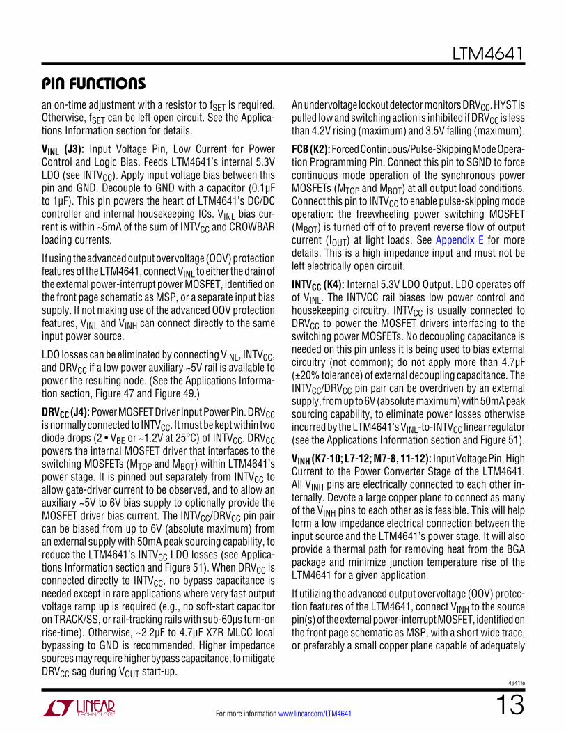
LTM4641
134641fe
For more information www.linear.com/LTM4641
pin FuncTionsan on-time adjustment with a resistor to fSET is required. Otherwise, fSET can be left open circuit. See the Applica-tions Information section for details.
VINL (J3): Input Voltage Pin, Low Current for Power Control and Logic Bias. Feeds LTM4641’s internal 5.3V LDO (see INTVCC). Apply input voltage bias between this pin and GND. Decouple to GND with a capacitor (0.1µF to 1µF). This pin powers the heart of LTM4641’s DC/DC controller and internal housekeeping ICs. VINL bias cur-rent is within ~5mA of the sum of INTVCC and CROWBAR loading currents.
If using the advanced output overvoltage (OOV) protection features of the LTM4641, connect VINL to either the drain of the external power-interrupt power MOSFET, identified on the front page schematic as MSP, or a separate input bias supply. If not making use of the advanced OOV protection features, VINL and VINH can connect directly to the same input power source.
LDO losses can be eliminated by connecting VINL, INTVCC, and DRVCC if a low power auxiliary ~5V rail is available to power the resulting node. (See the Applications Informa-tion section, Figure 47 and Figure 49.)
DRVCC (J4): Power MOSFET Driver Input Power Pin. DRVCC is normally connected to INTVCC. It must be kept within two diode drops (2 • VBE or ~1.2V at 25°C) of INTVCC. DRVCC powers the internal MOSFET driver that interfaces to the switching MOSFETs (MTOP and MBOT) within LTM4641’s power stage. It is pinned out separately from INTVCC to allow gate-driver current to be observed, and to allow an auxiliary ~5V to 6V bias supply to optionally provide the MOSFET driver bias current. The INTVCC/DRVCC pin pair can be biased from up to 6V (absolute maximum) from an external supply with 50mA peak sourcing capability, to reduce the LTM4641’s INTVCC LDO losses (see Applica-tions Information section and Figure 51). When DRVCC is connected directly to INTVCC, no bypass capacitance is needed except in rare applications where very fast output voltage ramp up is required (e.g., no soft-start capacitor on TRACK/SS, or rail-tracking rails with sub-60µs turn-on rise-time). Otherwise, ~2.2µF to 4.7μF X7R MLCC local bypassing to GND is recommended. Higher impedance sources may require higher bypass capacitance, to mitigate DRVCC sag during VOUT start-up.
An undervoltage lockout detector monitors DRVCC. HYST is pulled low and switching action is inhibited if DRVCC is less than 4.2V rising (maximum) and 3.5V falling (maximum).
FCB (K2): Forced Continuous/Pulse-Skipping Mode Opera-tion Programming Pin. Connect this pin to SGND to force continuous mode operation of the synchronous power MOSFETs (MTOP and MBOT) at all output load conditions. Connect this pin to INTVCC to enable pulse-skipping mode operation: the freewheeling power switching MOSFET (MBOT) is turned off of to prevent reverse flow of output current (IOUT) at light loads. See Appendix E for more details. This is a high impedance input and must not be left electrically open circuit.
INTVCC (K4): Internal 5.3V LDO Output. LDO operates off of VINL. The INTVCC rail biases low power control and housekeeping circuitry. INTVCC is usually connected to DRVCC to power the MOSFET drivers interfacing to the switching power MOSFETs. No decoupling capacitance is needed on this pin unless it is being used to bias external circuitry (not common); do not apply more than 4.7µF (±20% tolerance) of external decoupling capacitance. The INTVCC/DRVCC pin pair can be overdriven by an external supply, from up to 6V (absolute maximum) with 50mA peak sourcing capability, to eliminate power losses otherwise incurred by the LTM4641’s VINL-to-INTVCC linear regulator (see the Applications Information section and Figure 51).
VINH (K7-10; L7-12; M7-8, 11-12): Input Voltage Pin, High Current to the Power Converter Stage of the LTM4641. All VINH pins are electrically connected to each other in-ternally. Devote a large copper plane to connect as many of the VINH pins to each other as is feasible. This will help form a low impedance electrical connection between the input source and the LTM4641’s power stage. It will also provide a thermal path for removing heat from the BGA package and minimize junction temperature rise of the LTM4641 for a given application.
If utilizing the advanced output overvoltage (OOV) protec-tion features of the LTM4641, connect VINH to the source pin(s) of the external power-interrupt MOSFET, identified on the front page schematic as MSP, with a short wide trace, or preferably a small copper plane capable of adequately

LTM4641
144641fe
For more information www.linear.com/LTM4641
pin FuncTionshandling the input current to LTM4641’s power stage. Do not decouple the VINH pins with any bypass capacitance in this case. Instead, place all decoupling capacitance directly between the drain of MSP to GND.
If not utilizing the advanced OOV protection features of the LTM4641, do decouple the VINH pins to GND with local ceramic and bulk decoupling capacitance (see the Applications Information section).
PGOOD (L1): Output Voltage Power Good Indicator. This is an open-drain logic output pin that is pulled to ground when the output voltage (and accordingly, the divided-down representation of the output voltage, VFB, as presented to the control loop) is outside ±10% of the nominal target for regulation.
TRACK/SS (L2): Output Voltage Tracking and Soft-Start Programming Pin. This pin has a 1.0μA pull-up current source, typical. A capacitor can be placed from this pin to
SGND to obtain an output voltage soft-start ramp-up rate whose turn-on time is 0.6ms per nanofarad of capacitance. Alternatively, when a voltage is applied to TRACK/SS through a resistor-divider network from another rail, the LTM4641 output is able to track the external voltage to satisfy coincident and ratiometric rail-voltage sequencing requirements. See the Applications Information section.
VING (M9): Gate Drive Output Pin. If utilizing the advanced output overvoltage (OOV) protection features of the LTM4641, connect VING to VINGP and to the gate of the external power-interrupt N-channel MOSFET feeding VINH, identified on the front page schematic as MSP; otherwise, leave this pin electrically open circuit.
VINGP (M10): Gate Drive Protection Pin. If utilizing the ad-vanced OOV protection features of the LTM4641, connect VINGP to VING and to the gate of the external power-interrupt N-channel MOSFET feeding VINH, MSP; otherwise, leave this pin electrically open circuit.
LTM4641
154641fe
For more information www.linear.com/LTM4641
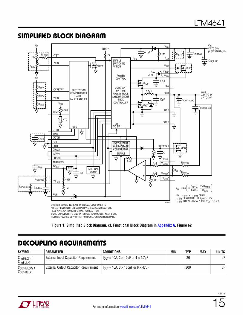
siMpliFieD block DiagraM
Decoupling requireMenTs
Figure 1. Simplified Block Diagram. cf. Functional Block Diagram in Appendix A, Figure 62
SYMBOL PARAMETER CONDITIONS MIN TYP MAX UNITS
CIN(MLCC) + CIN(BULK)
External Input Capacitor Requirement IOUT = 10A, 2 × 10μF or 4 × 4.7μF 20 μF
COUT(MLCC) + COUT(BULK)
External Output Capacitor Requirement IOUT = 10A, 3 × 100μF or 6 × 47μF 300 μF
+
–
+
8.2k
RSET2
R C
MCB
MBOT
10µF
CIN(MLCC)0.1µF
2.2µF
COUT(MLCC)
VOUT0.6V TO 6VUP TO 10A
VIN4V TO 38V(4.5V START-UP)
COUT(BULK)
+CIN(BULK)
8.2k
8.2k RSET1B
RSET1A
4641 F01
VORB+
VORB–
CROWBAR
DASHED BOXES INDICATE OPTIONAL COMPONENTS*RfSET REQUIRED FOR CERTAIN VIN/VOUT COMBINATIONS SEE APPLICATIONS INFORMATION SECTIONSGND CONNECTS TO GND INTERNAL TO MODULE, KEEP SGNDROUTES/PLANES SEPARATE FROM GND, ON MOTHERBOARD
SGND
VOSNS+
VOSNS–8.2k
ENABLE
FAST OUTPUTOVERVOLTAGECOMPARATOR
POWERCONTROL
ENABLESWITCHINGACTION
CONSTANTON-TIME
VALLEY MODESYNCHRONOUS
BUCKCONTROLLER
MSP
RfSET*1.3M10k
VFBTO E/A
GND
SW
15VZENER
VOUT
VINH
VINGP
VING
VINL
fSETION
INTVCC
VIN
VIN
0.8µH
MTOP
MHYST
HYSTRHYSTRTUV
RBUV
RTOV
RMOV
RBOV
3.48k
499k
1M
1VREF
NTC
UVLO
IOVRETRY
OVLO
TEMP
OTBH
LATCHTMR
FCB
COMPDRVCC
INTVCC
PGOOD
PROTECTIONCOMPARATORS
ANDFAULT LATCHES
OSC
REF
CTMR
CSS
4µF
TRACK/SS1VREF
OVPGM
RUN
RTOVPGM
RBOVPGM COVPGM
INTERNALCOMP
USE RSET1A = RSET1B ≤8.2kRSET2 REQUIRED FOR VOUT > 1.2VRSET2 NOT NECESSARY FOR VOUT ≤ 1.2V
VOUT = 0.6 1+ RSET1A
8.2kΩ+ 2 •RSET1A
RSET2
LTM4641
164641fe
For more information www.linear.com/LTM4641
operaTionIntroduction
The LTM4641 contains a buck-topology regulator employ-ing a constant on-time current mode control scheme, including built-in power MOSFET devices with fast switching speed and a power inductor. In its most basic configuration (see Figure 45), the module operates as a standalone nonisolated switching mode DC/DC step-down power supply. It can provide up to 10A of output current with a few external input and output capacitors and output feedback resistors. The supported output voltage range is from 0.6V DC to 6V DC. The supported input voltage range is 4V to 38V, with a maximum start-up voltage of 4.5V (over temperature). Power conversion from lower input voltages can be realized if an auxiliary bias supply is avail-able to power LTM4641’s control and housekeeping bias input pin, VINL. The LTM4641 Simplified Block Diagram is found in Figure 1. For a more detailed look, the Functional Block Diagram is found in Appendix A, Figure 62.
Motivation
Pulsed loading conditions and abnormal disturbances within the electrical systems found in industrial, vehicle, aeronautic, and military applications can induce wildly varying voltage transients (surges) on what is nominally a 24V DC to 28V DC distributed bus (28V DC bus). The duration of such disturbances can extend for periods of time between a millisecond to a minute in length, with excursions sometimes reaching (or exceeding) 40V and falling below 6V.
While switching buck regulators are of universal inter-est due to their compact size and ability to deliver DC/DC power conversion at high efficiency, FMEA (failure modes and effects analysis) leads one to believe that there is no way to reduce the severity rating and effects of an electrical short from the input source to the output load—however improbable. The LTM4641 challenges this notion by protecting the load from seeing excessive voltage stress, even when its high side switching MOSFET is short circuited.
Power µModule Regulator Reliability
First and foremost, Linear Technology μModule products adhere to rigorous testing and high reliability control, fabrication, and manufacturing processes—as is required of all its products. Furthermore, as part of its commit-ment to excellence, the Linear Technology Quality Control program periodically updates its Reliability Data report for LTM4600 series products to include cumulative data obtained from ongoing and routine in-house testing relating to operational life, highly accelerated stress, power and temperature cycling, thermal and mechanical shock, and much more. To view the latest report visit http://www.linear.com/docs/13557.
The LTM4641 easily supports high step-down ratios with few external components. The additional protection features when implemented provide an extra degree of insurance beyond other μModule regulators.
Overview
When configured as shown in Figure 46, the LTM4641 can regulate an output voltage between 0.6V and 6V from an input voltage between 4V and 38V (4.5VIN start-up, maximum).
If an optional N-channel power MOSFET, MSP, is placed between the input power source (VIN) and the power stage input pins (VINH), MSP’s role becomes that of a resettable electronic power-interrupt switch. The gate of MSP is operated by VING, and its gate-to-source voltage is assured to be clamped by a built-in 15V Zener diode accessed via VINGP. When switching action is engaged, VING charges the gate of MSP to nominally 10V above VINH potential—suitable for driving a standard-logic MOS-FET—and MSP becomes enhanced to pull VINH up to the input source supply’s electrical potential. The switching regulator steps down VINH potential to VOUT when MSP is on. When switching action is inhibited by pulling the RUN pin low or when a fault condition is detected by LTM4641’s internal circuitry—such as an output overvoltage (OOV) condition—the gate of MSP is discharged and MSP turns off. The input source supply is thus disconnected from LTM4641’s power stage input (VINH).

LTM4641
174641fe
For more information www.linear.com/LTM4641
applicaTions inForMaTion—power supply FeaTuresThe operation of MSP as a power interrupter provides a critical element of robust OOV protection: it removes a means for input power to flow through a damaged power stage to any precious loads on the output voltage rail, even when input power is cycled.
For even greater resilience to a short-circuit between VINH and the SW switching node of the power stage, an external logic-level N-channel power MOSFET, MCB, is optionally placed—in a crowbar configuration—on the output of the power module. When an OOV condition is detected, CROWBAR turns on MCB (within 500ns, maximum) to discharge the output capacitors and transform any residual energy in LTM4641’s power stage into a trivial amount of heat—energy which would otherwise have only served to inject charge into (further pump up the voltage on) the output capacitors, where precious loads reside.
The control and monitoring circuitry within the LTM4641 power module provide the following:
• Fast, accurate, latching output overvoltage detector (<500ns response time, <±12mv threshold error)
• N-channel output overvoltage crowbar power MOSFET drive
• Accurate (<±2.4%) nonlatching and resettable latching input overvoltage shutdown thresholds
• N-channel overvoltage power-interrupt MOSFET drive
• Accurate (<±2.4%) Input UVLO rising and UVLO falling thresholds
• Built-in and adjustable overtemperature shutdown protection, programmable for resettable latching or nonlatching (hysteretic restart) response
• Analog temperature indicator output pin
• Adjustable power-on reset and timeout delay time
• Latchoff behavior that can be altered to instead provide autonomous restart after timeout delay time expires
• Parallelable for higher output power
• Differential remote sensing of POL voltage
• Internal loop compensation
• Output current foldback protection
• Selectable pulse-skipping mode operation
• Output voltage soft-start and rail tracking
• Power-up into pre-biased conditions without sinking current from the output capacitors
• Adjustable switching frequency
• Power good indicator
• RUN enable pin
Novel and simple circuit implementations with LTM4641 and a few external components enable surge ride-through protection and overtemperature detection of a power-interrupt MOSFET. (See Figure 47, for example.) The aforementioned features enabled by LTM4641 are grouped by function and described in the remainder of the Applica-tions Information section.
Power (VINH) and Bias (VINL) Input Pins
LTM4641’s power stage (VINH) and control bias (VINL) input pins are brought out separately to allow freedom for implementing more sophisticated system configura-tions, such as: fully utilizing LTM4641’s advanced output overvoltage (OOV) protection features to protect the load (e.g., front page schematic or Figure 46); providing rudi-mentary input surge ride-through protection (Figure 47); performing DC/DC down conversion from a power rail below LTM4641’s inherent UVLO thresholds (from a 3.3V bus in Figure 49).
If VINH and VINL are powered from separate rails, it is recommended to power up VINL prior to or concurrently with VINH. VINL should have a final value of at minimum 3.5V within 2ms of VINH exceeding 3.5V. The recommen-dation to sequence VINL ahead of or closely with VINH is not related at all to module device reliability but stems rather from a desire to assure that the control section of LTM4641 drives the MOSFETs in LTM4641’s power stage deterministically whenever any appreciable VINH voltage is present. It is always permissible for VINL voltage to be present—regardless of the state of VINH—however, realize that there is no UVLO detection on VINH.
To prevent the control section from trying to regulate through a dropout condition or commencing switching activity in the absence of VINH potential, it is recommended

LTM4641
184641fe
For more information www.linear.com/LTM4641
applicaTions inForMaTion—power supply FeaTuresto implement a custom UVLO falling setting above the dropout curve in Figure 4 (see also Figure 11).
LT3010-5 is shown in Figure 47 to provide bias for VINL, to enable ride-through of 80V transients on VIN. UVLO detection of VIN is realized in this example by D2 creating a discharge path for VINL in the event of loss of VIN.
VINH and VINL have no specific power-down sequenc-ing requirement, only that VINL should stay above 3.5V whenever VINH is above 3.5V.
VINL and VINH sequencing is inherently addressed by the LTM4641 in the Figure 45 and Figure 46 circuits.
The VIN and VINL start-up and shutdown waveforms of the Figure 47 circuit—but with 1Ω output load and TMR tied to INTVCC—are shown in Figure 2. The effect of the tim-ing capacitor, CTMR, that normally generates a power-on reset (POR) delay at start-up is negated by tying TMR to INTVCC. The ~3ms VIN-to-VOUT start-up delay time seen in Figure 2 is due to POR of the LTM4641’s fault-monitoring circuitry and soft-start ramp (CSS).
scheme. During a load transient step-up, the control loop will command a higher inductor trough current to compensate for a deficiency in output voltage; the effective switching frequency will increase until the output voltage returns to normal (an overcurrent event, notwithstanding). During a load transient step-down, the control loop will command a lower inductor trough current to compensate for an excess of output voltage; the effective switching frequency will decrease until the output voltage returns to normal. The control loop perceives inductor current-sense information via the voltage signal that appears across the synchronous power MOSFET, MBOT, when MBOT is on (this is commonly referred to in the industry as RDS(ON) current sensing).
The on-time of the one-shot timer—and hence the power control MOSFET, MTOP,—is given, in units of seconds, by:
tON = 0.7V • 10pF
IION (1)
where IION is in units of amperes. For output voltages greater than 3V, and for non-rail-tracking applications, no external RfSET resistor is needed, and the IION current (units: amperes) is set solely by the VINL voltage (units: volts) and the internal 1.3MΩ VINL-to-fSET resistor:
IION = VINL
1.3MΩ (2)
The switching frequency of operation of the LTM4641’s buck converter power stage at full load in this scenario is given, in Hz, by:
fSW = VOUT
0.7V • 1.3MΩ • 10pF (3)
where VOUT is the desired nominal output voltage, in units of volts.
An external RfSET resistor can be applied when setting VOUT greater than 3V, if desired, to obtain increased switching frequency. Usually, increasing switching frequency comes from a desire to reduce output voltage ripple and/or output capacitance requirement—but at a moderate penalty to DC/DC conversion efficiency. There are some limitations to how low an RfSET value can be applied in practice due
Figure 2. Start-Up and Shutdown Waveforms of Figure 47 Circuit. TMR Tied to INTVCC to Highlight VIN and VINL Sequencing without POR Delay. 1Ω Load
2ms/DIV 4641 F02
VOUT500mV/DIV
VINL5V/DIV
VIN5V/DIV
Switching Frequency (On Time) Selection and Voltage Dropout Criteria (Achievable VIN-to-VOUT Step-Down Ratios)
The LTM4641 controller employs a current mode constant on-time architecture, in which the COMP voltage corre-sponds to the trough inductor current at which the internal high side power MOSFET (MTOP) is commanded on by the control loop—for a duration of time proportional to controller’s ION pin current (Refer to Figure 1). Regulation is maintained by a pulsed frequency modulation (PFM)

LTM4641
194641fe
For more information www.linear.com/LTM4641
applicaTions inForMaTion—power supply FeaTuresto non-zero minimum off-time, dropout voltage, and maximum achievable switching frequency of operation.
When an RfSET resistor external to the LTM4641 is con-nected between VINL and fSET to decrease the default on-time setting, the total ION current (units: amperes) is given by:
IION = VINL
1.3MΩ+ VINL
RfSET= VINL
1.3MΩ ||RfSET (4)
where VINL is in units of volts and RfSET is in units of ohms. RfSET is needed for output voltage settings less than or equal to 3VOUT, and for rail-tracking applications.
The minimum on-time the LTM4641 supports is 43ns, typi-cal, but guard banded conservatively to 75ns, maximum. Therefore, for a conservative design, tON should be larger than 75ns, typical. From Equation 1, it follows that IION should be designed to be less than 93.3μA.
When an external RfSET resistor is applied between VINL and RfSET (and VINL and VINH are operating from the same rail—Figure 45 and Figure 46), the switching frequency of operation of the power stage at full load, in Hz, is given by:
fSW = VOUT
0.7V • 1.3MΩ ||RfSET( ) • 10pF (5)
where RfSET is in ohms, and VOUT is the desired nominal output voltage, in units of volts.
In the general case, the switching frequency of the buck converter power stage at full load is given, in Hz, by:
fSW = VOUT
VINH • tON= VOUT • IION
VINH • 0.7V • 10pF (6)
See Appendix C for a detailed discussion on the following topics:
• Why should the switching controller be operated at a higher switching frequency (i.e., programmed for a shorter on-time with RfSET) than that yielded by the internal 1.3MΩ VINL-to-fSET resistor alone…
…for nominal output voltages of 3V and less?
…in rail-tracking applications?
• When VINL and VINH are operated from separate supplies…
… why should RfSET ordinarily connect to the VIN power source rather than VINH (Figure 49)?
…when is it okay for RfSET to connect to VINH (Figure 47)?
For application circuits of the form found in Figure 45, Figure 46, Figure 47 and Figure 51: see Figure 3 for the maximum recommended value of RfSET as a function of nominal target output voltage, and resulting full-load switching frequency corresponding to those RfSET values.
Figure 3 can also be interpreted to provide the lowest recommended switching frequency for a given target output voltage. Table 1 summarizes nominal values of RfSET endorsed for some popular output voltages; use of commonly available ±5% tolerance resistors or better with ±100ppm/°C temperature coefficient or better is recommended.
Figure 3. Maximum Recommended RfSET (Nominal Values) for Non-Tracking Applications, and Resulting Full-Load Operating Switching Frequency vs Nominal Output Voltage
NOMINAL OUTPUT VOLTAGE (V)0 0.5 1 1.5
MAX
IMUM
REC
OMM
ENDE
D R f
SET
VALU
E (M
Ω)
TYPICAL fSW AT FULL LOAD (kHz)
1
5
10
50
100
2 2.5 3 3.5 4 4.5 5 5.5 6
4641 F03
0.1
0.5
500
600
700
0
200
300
100
400
RfSET vs VOUTREGION
TO AVOID
RfSET NOTNEEDED FORVOUT > 3V
MAX RECOMMENDED RfSETSWITCHING FREQUENCY

LTM4641
204641fe
For more information www.linear.com/LTM4641
applicaTions inForMaTion—power supply FeaTuresTable 1. Endorsed RfSET Resistor Value vs Output Voltage for Non-Tracking Applications—and Resulting Full-Load Switching Frequency (cf. Figure 45, Figure 46, Figure 47, and Figure 51 Circuits)
VOUT(NOM) (V)RfSET (MΩ) (Nearest EIA-Standard Values) fSW (kHz)
0.6 0.787 175
0.7 0.825 200
0.8 0.887 215
0.9 0.931 235
1.0 1.00 255
1.2 1.13 285
1.5 1.43 315
1.8 2.00 325
2.0 2.55 330
2.5 5.76 335
Greater Than 3.0 ∞ (Not Used) See Figure 2
3.3 ∞ (Not Used) 360
5.0 ∞ (Not Used) 550
6.0 ∞ (Not Used) 660
In rail-tracking applications, it is recommended to use the RfSET value corresponding to the lowest voltage needed to be regulated during output voltage ramp down. For example: to ramp VOUT down to 0.5V requires RfSET to be not more than 750kΩ (nominal) per Figure 3.
It is often permissible to use lower RfSET values than those indicated in Figure 3 and Table 1 if, for example, lower output ripple voltage and/or a lower output capacitance is desired. However, be aware of three guiding principles:
I. Minimum On-Time. Ensure IION < 93.3µA. See Equa-tions 1 and 4.
II. Minimum Off-Time and Dropout Operation. The mini-mum off-time, tOFF(MIN), is the shortest time required for the LTM4641 to perform the following tasks: turn on its power synchronous MOSFET (MBOT), trip the control loop’s current comparator, and turn off MBOT. The minimum input voltage on VINH, in volts, that one can regulate the output at and still avoid dropout is given by:
VIN(DROPOUT) = VOUT • 1+
tOFF(MIN)
tON
+RPS • IOUT
(7)
where:
• VOUT is nominal output voltage in volts.
• tOFF(MIN) is the minimum length of time MBOT can be on, after MTOP turns off. For a conservative de-sign, use a value of 300ns, taken from the Electrical Characteristics Table.
• tON is the on-time of the power control MOSFET, MTOP, as programmed by the current flowing into the ION pin of LTM4641’s internal control IC.
• RPS is the series resistance of the module’s power stage, from VINH to VOUT. For VIN ≥ 6V, this is less than 50mΩ, even at extreme temperatures (TJ ≈ 125°C). For VIN < 6V, the effective series resistance increases due to drop in INTVCC voltage and cor-responding decreased gate-drive enhancement of MTOP. Printed circuit board (PCB) and/or cable resistance present in the copper planes and/or wires that physically connect the output of the module to the load adds to RPS’s effective value.
• IOUT is the load current on VOUT in amperes.
For applications of the form shown in Figure 45, Fig-ure 46 and Figure 47: the minimum allowable VINH voltage of operation to avoid dropout for 3V < VOUT ≤ 6V is shown in Figure 4. The curves are a result of realizing that VIN(DROPOUT) equals VINH (neglecting MSP voltage drop) when dropout actually occurs, and that Equations 1 and 2 yield an expression for tON as a function of VINH. MTOP will be less fully enhanced during its on-time if DRVCC is less than its nominal value of 5.3V (for example, when VINL< 6V and when DRVCC bias is provided by INTVCC). DRVCC’s effect on RPS at low line is illustrated in Figure 4.
III. Maximum Attainable fSW. The maximum attainable switching frequency of operation (in units of Hz) for a given on-time (tON, in seconds) is governed simply by:
fMAX = 1
tON + tOFF(MIN) (8)
where a conservative value of 300ns can be used for tOFF(MIN).

LTM4641
214641fe
For more information www.linear.com/LTM4641
applicaTions inForMaTion—power supply FeaTures
Figure 4. Line Dropout Voltage vs Output Voltage at No Load and Full Load. Figure 45, Figure 46 and Figure 47 Circuit Applications. RfSET = Open and RSET1A, RSET1B, RSET2 Values Setting VOUT for Regulation at or Above 3V
Given that the PFM control scheme increases switching frequency (to as high as fMAX) to maintain regulation during a transient load step-up, the design guidance is: set the steady-state operating frequency fSW to be less than fMAX. Furthermore, when the LTM4641 is in dropout operation, the switching frequency of the converter is fMAX.
It is best to avoid operation in dropout scenarios, because the control loop will rail COMP high to command MTOP at highest possible duty cycle. If input voltage “snaps upwards” at a sufficiently high slew rate when COMP has railed, the control loop may be unable provide satisfactory line rejection.
See Figure 11 to set the UVLO falling response of LTM4641 above the computed VIN(DROPOUT) voltage; this will inhibit switching action for VIN < VIN(DROPOUT). Input voltage ripple, and any line sag between the input source supply and the VINH pins—and voltage drop across the power interrupt MOSFET, MSP, if used—must be taken into account by the system designer.
Setting the Output Voltage; the Differential Remote Sense Amplifier
A built-in differential remote-sense amplifier enables preci-sion regulation at the point-of-load (POL), compensating for any voltage drops in the system’s output distribution path: the total variation of LTM4641’s output DC voltage over line, load, and temperature is better than ±1.5%.
The basic feedback connection between the POL and the module’s feedback sense pins is shown in Figure 5.
Figure 5. Basic Feedback Remote Sense Connections and Techniques; Setting the Output Voltage
+
–
+8.2k VOSNS
+
VOSNS–
VORB+
VORB–
SGND
ICTTESTPOINT
VOUT
COUT(BULK) COUT(MLCC)
RSET2
RSET1A
CFFB
CFFA
ICTTESTPOINT
SGND CONNECTS TO GND INTERNAL TO MODULE. KEEPMODULE SGND ROUTES/PLANES SEPARATE FROM GNDON MOTHERBOARD
4641 F05
PLACE ALLFEEDBACK
COMPONENTSLOCAL TO THE
LTM4641
VFBTO ERRORAMPLIFIER
8.2k
8.2k
8.2k
LTM4641
TRUE DIFFERENTIAL REMOTESENSE AMPLIFIER
GND
VOUT
RSET1B
ROUTE FEEDBACK SIGNAL ASA DIFFERENTIAL PAIR (OR
TWISTED PAIR IF USING WIRES).SANDWICH BETWEEN GROUND
PLANES TO FORM A PROTECTIVE SHIELDGUARDING AGAINST STRAY NOISE
LOAD
CFFA, CFFB: FEEDFORWARD CAPACITORS YEILD IMPROVED TRANSIENTRESPONSE WHEN FILTERING VOUT WITH ONLY MLCC OUTPUT CAPACITORS(COUT(MLCC))
OUTPUT VOLTAGE SETTING (V)3
LINE
DRO
POUT
VOL
TAGE
(V)
6.0
7.0
8.0
54641 F04
5.0
4.0
5.5
6.5
7.5
4.5
3.5
3.03.5 4 4.5 5.5 6
10A OUTPUT, DRVCC BIASED FROM INTVCC (5.3VNOM)10A OUTPUT, DRVCC BIASED TO 5.3V BY EXTERNAL SUPPLYNO LOAD, DRVCC ≥ 4.2V(UVLO RISING) AND 3.5V (UVLO FALLING)
LTM4641
224641fe
For more information www.linear.com/LTM4641
applicaTions inForMaTion—power supply FeaTuresThe output voltage at the POL is differentially sensed via a symmetrical impedance-divider network. In Figure 1 and Figure 5, it is seen that the control loop regulates the output voltage such that the differential VOSNS
+-to-VOSNS–
feedback signal voltage is the lesser of the TRACK/SS pin voltage or the regulator’s nominal bandgap voltage of 600mV. The arrangement and values of the resistors in the symmetrical impedance-divider network set the output voltage.
The remote sense pins (VOSNS+, VOSNS
–) have redundant connections internal to the module to readback pins (VORB
+, VORB–). The readback pins provide a means to
verify the integrity of the feedback signal connection dur-ing motherboard ICT (in circuit test). The importance of verifying the integrity of the connection of the feedback signal to the output voltage prior to powering up the input voltage cannot be understated. If one or both feedback pins are left electrically floating due to manufacturing as-sembly defect, for example, or if the remote-sense pins are short circuited to each other, the control loop and overvoltage-detector circuitry have no awareness of the actual output voltage condition. A compromised feedback connection presents a very real danger of (1) the control loop commanding on MTOP at the highest possible duty cycle—due to the lack of negative feedback—and (2) the LTM4641’s protection circuitry being unaware of any issue. In a production environment, modern day ICT can easily catch any such stuffing or assembly errors; in a lab or prototyping environment, an ohmmeter can do the job.
For many applications that use a mixture of MLCC and bulk (low ESR tantalum or polymer) output capacitors, the symmetrical impedance-divider network that feeds back the POL’s voltage to the module need only be constructed with resistors RSET1A and RSET1B, for output voltages of 1.2VOUT and lower. RSET2 must be present for output voltages in excess of 1.2VOUT. RSET1A and RSET1B should always have the same nominal value. Applications with MLCC-only output capacitors (see Output Capacitors and Loop Stability in following pages) will demonstrate improved transient response when feedforward capaci-tors CFFA and CFFB, nominally equal in value, are installed electrically in parallel with RSET1A and RSET1B, respectively.
Use of 0.1% tolerance resistors (or better) for RSET1A, RSET1B, and RSET2 are recommended—with temperature coefficients of resistance suitable for one’s operating range of PCB temperature—to assure that output voltage error introduced by resistor value variation is acceptable for the application. SMT resistors with T.C.R.s of ±25ppm/°C and better are readily available in the marketplace.
For output voltage settings less than or equal to 1.2VOUT, RSET2 is not needed, and RSET1A and RSET1B are given by:
RSET1A = RSET1B = VOUT
0.6V– 1
• 8.2kΩ
(9)
For output voltages above 1.2VOUT, RSET1A (and RSET1B) should be set equal to 8.2kΩ (or less, if 8.2kΩ is not a convenient value for the user), and RSET2 is then given by:
RSET2 = 2 •RSET1AVOUT0.6
– RSET1A8.2kΩ
− 1
(10)
It is always permissible to select a value for RSET1A (and RSET1B) less than that given by Equation 9—and then calculate a valid value for RSET2 from Equation 10—as long as RSET1A and RSET1B are designed to withstand the higher resulting power dissipation.
When VOUT is in regulation, the voltages at VOSNS+ and
VOSNS– are given by:
VVOSNS+ = 0.6V
8.2kΩ ||RSET1A ||RSET2( )+ ∆VGND
RSET1A
• RSET1A || 16.4kΩ( )
(11)
and
VVOSNS– = VVOSNS
+ – 0.6V (12)
respectively. ∆VGND is the voltage drop between ground at the POL and LTM4641’s SGND pins in volts. This voltage drop is usually entirely a result of I • R drop in the output distribution path—largest when maximum load current is being drawn:
∆VGND = VGND(POL) – VSGND(LTM4641) (13)

LTM4641
234641fe
For more information www.linear.com/LTM4641
applicaTions inForMaTion—power supply FeaTuresWith RSET1A, RSET1B, and RSET2 determined, double-check the output voltage setting with:
VOUT = 0.6V • 1+ RSET1A
8.2kΩ+ 2 •RSET1A
RSET2
(14)
Some recommended values for RSET1A, RSET1B, and RSET2 for popular output voltages are shown in Table 2.
Table 2. Recommended RSET1A, RSET1B and RSET2 Values for Some Popular Output Voltages, cf. Figure 5 Feedback Connections.
VOUT RSET1A, RSET1B RSET2
0.6V 0Ω ∞ (Not Used)
0.7V 1.37kΩ ∞ (Not Used)
0.8V 2.74kΩ ∞ (Not Used)
0.9V 4.12kΩ ∞ (Not Used)
1.0V 5.49kΩ ∞ (Not Used)
1.2V 8.2kΩ ∞ (Not Used)
1.5V 8.2kΩ 33.2kΩ
1.8V 8.2kΩ 16.5kΩ
2.0V 8.2kΩ 12.4kΩ
2.5V 8.2kΩ 7.5kΩ
3.3V 8.2kΩ 4.7kΩ
5.0V 8.2kΩ 2.61kΩ
6.0V 8.2kΩ 2.05kΩ
See Appendix D for a detailed discussion on the following topics:
• What is the rationale for using a symmetrical resistor network?
• What should I do if I cannot shield the differential sense feedback lines with GND? (I anticipate differential mode noise in the feedback signal?)
• What should I do if the module and the load(s) are separated by a significant distance (~50cm or more), or if the load current flows through a cable assembly or power connector? (I anticipate common mode noise in the feedback signal?)
Input Capacitors
The LTM4641 module should be connected to a low AC impedance, nominally DC output voltage source. MLCC input bypass capacitors must be provided externally, as
close in proximity to the module as possible (see Figure 43). If external MOSFET MSP is not used (Figure 45), two 10μF or four 4.7μF ceramic capacitors should be electrically connected directly between the VINH and GND pins. If MSP is used (Figure 46, Figure 47 and Figure 49), then MSP must be placed as close to the LTM4641’s VINH pins as possible, and two 10μF or four 4.7μF ceramic capacitors should be electrically connected directly between the drain of MSP and GND (see Figure 44). A 47μF to 100μF surface mount bulk capacitor can be used to supplement input power bypassing, and can share the burden of any local ceramic capacitors in filtering the power stage’s ripple current. If low impedance power planes are used to bring VIN to the vicinity of the module, input source impedance will be low enough that bulk capacitors will not be needed. A localized bulk input capacitor is needed when an underdamped LC-resonant tank is formed by routing long input leads or traces (low ESR inductance) bypassed only with MLCCs (ultralow ESR capacitance).
Neglecting the inductor peak-to-peak current ripple, the RMS current of the input capacitor can be estimated as:
ICIN(RMS) =
IOUT(MAX)
η• D • 1– D( )
(15)
where η is the power conversion efficiency of the LTM4641 module and D is the duty cycle on-time of MTOP. The bulk capacitor can be a switcher-rated electrolytic aluminum capacitor or a polymer capacitor.
For a buck converter, the switching duty cycle of MTOP can be estimated as:
D = VOUT
VIN (16)
Output Capacitors and Loop Stability/Loop Compensation
The current mode constant on-time architecture enables very high step-down input-to-output ratios with compel-ling transient response. It also enables cycle-by-cycle fast current limit and foldback current limit in an overcurrent condition. The LTM4641 is internally compensated to yield stability over all operating conditions.

LTM4641
244641fe
For more information www.linear.com/LTM4641
applicaTions inForMaTion—power supply FeaTuresThe output capacitors COUT(BULK) and COUT(MLCC) must be chosen with low enough effective series resistance (ESR) to meet the output voltage ripple requirements and provide localized bypassing for the load. Although the LTM4641 provides fast transient response, the output voltage at the POL is reliant on nearby charge stored in a reservoir of ceramic capacitors COUT(MLCC) to minimize sag and overshoot in the initial microseconds of a high dI/dt transient load step-up and step-down, respectively. If used, COUT(BULK) can be comprised of low ESR tantalum or low ESR polymer capacitor(s); these capacitors then serve as a local reservoir to replenish the MLCCs during transient load events. It is also possible to use COUT(MLCC)only, however, the use of feedforward capacitors, CFF, should then be installed in the remote-sense feedback path, to obtain an optimized transient response (see Figure 5 feedback connections).
The COUT(MLCC) ceramic capacitors should be at least X5R-type material. X5R-type and X7R-type MLCCs are recommended when operating PCB temperatures are not more than 85°C and 125°C, respectively. Both materials are renown in the industry for having a relatively low ca-pacitance change over their respective temperature range of operation (±15%). However, X5R and X7R MLCCs do exhibit significant loss of capacitance with applied DC voltage and are subject to aging effects, and this must be taken into account in any system design. Refer to the capacitor manufacturer’s specifications for details.
The typical output capacitance range is between 200μF to 800μF. The system designer should use discretion in determining whether additional output filtering may be needed, if further reduction of output ripple—or output voltage deviation during dynamic load or line transient events—is required.
In Table 9, guidelines are provided for output capacitor selection, for various operating conditions. The table optimizes total equivalent ESR and total bulk capacitance for the transient load step performance. Stability criteria is considered. The Linear Technology LTpowerCAD™ de-sign tool is available for transient simulation and stability analysis, if desired.
Pulse-Skipping Mode vs Forced Continuous Mode
In applications where high DC/DC conversion efficiency at light-load currents is highly desired—when the input voltage source is a battery, for example—pulse-skipping mode operation should be employed. Pulse-skipping mode operation prevents power flow from the output capacitors to the input source. Be aware, however, due to MBOT’s re-sulting asynchronous operation at light load, applications employing pulse-skipping mode may necessitate more output capacitance and/or a higher OVPGM setting than operation in forced continuous mode would.
Pulse-skipping mode is activated by connecting FCB to INTVCC. Forced continuous operation is activated by con-necting FCB to SGND.
Be aware that in pulse-skipping mode and ultralight loads (say, less than 20mA out), the VING voltage may appear as a sawtooth waveform as a result of being charge-pumped at a slower rate, to conserve energy.
See Appendix E for more information on how pulse-skipping mode works.
Soft-Start, Rail-Tracking and Start-Up Into Pre-Bias
The TRACK/SS pin can be used to either soft-start the output of the LTM4641 regulator, or make LTM4641’s output voltage track another rail coincidentally or ratio-metrically. When RUN or HYST is low, the TRACK/SS pin is discharged. When RUN and HYST are released, TRACK/SS sources a microamp of current.
When a soft-start capacitor, CSS, is applied to the pin, the current source is responsible for generating an output volt-age turn-on time of 0.6ms per nanofarad of capacitance. The power stage is high impedance (MTOP and MBOT are off) until the TRACK/SS pin voltage exceeds VFB, the remote-sense differential amplifier’s output voltage. This allows power-up into pre-biased output voltage conditions without sinking of current from the output capacitors. When TRACK/SS exceeds the control IC’s 600mV bandgap voltage, VFB is regulated at 600mV and VOUT reaches its nominal output voltage.

LTM4641
254641fe
For more information www.linear.com/LTM4641
applicaTions inForMaTion—power supply FeaTuresFigure 6 shows idealized output voltage waveforms for applications in which LTM4641’s output (VOUT) tracks a master rail (VMASTER) coincidently and ratiometrically, respectively.
(3) Choose output capacitors and input capacitors for the design in the same manner as is done for nontracking applications.
To fulfill a coincident rail-tracking requirement, recognize that when the output voltage of the master rail reaches the tracking rail’s nominal FS voltage, the TRACK/SS pin of the LTM4641 (tracking slave) needs to be 600mV. This can be satisfied by forming a resistor-divider network composed of RTAC and RTBC, interfacing VOUT_MASTER to TRACK/SS of the LTM4641 tracking slave, and terminating to SGND of the LTM4641 tracking slave. In Figure 7 and Figure 8, U1 generates a master rail while U2 generates a coincident-tracking rail that follows U1’s output. Values of RTAC and RTBC are selected such that:
RTAC =
VOUT_SLAVE_C (FS OUTPUT)
0.6V– 1
•RTBC
(17)
In the example circuit of Figure 7, the master rail generated by U1 ramps up its output to 1.8V. The coincident-tracking rail is generated by U2 and has a nominal FS output voltage of 1V. Values of RTAC and RTBC are determined such that when U1’s output reaches 1V, the TRACK/SS pin of U2 reaches ~600mV; choosing RTBC to be 10kΩ yields RTAC = (1V/0.6V – 1) • 10kΩ, or ~6.65kΩ. It is common to choose resistor values of 10k or less for this task, so that voltage offset errors introduced by the 1µA current source on TRACK/SS working into the RTAC/RTBC network are sufficiently small.
To fulfill a ratiometric rail-tracking requirement, recognize that when the output voltage of the master rail reaches its final FS value, the TRACK/SS pin of the LTM4641 (tracking slave) needs to reach 600mV. This can be satisfied by forming a resistor-divider network composed of RTAR and RTBR, interfacing VOUT_MASTER to TRACK/SS of the LTM4641 tracking slave, and terminating to SGND of the LTM4641 tracking slave. In Figure 7 and Figure 8, U3 generates a ratiometric-tracking rail that follows U1’s output. Values of RTAR and RTBR are selected such that:
RTAR =
VOUT_MASTER (FS_OUTPUT)
0.6V– 1
•RTBR
(18)
TIME
VMASTER
VOUT
OUTP
UT V
OLTA
GE
4641 F06a
TIME
VMASTER
VOUT
OUTP
UT V
OLTA
GE
4641 F06b
(6a) Coincident Tracking
(6b) Ratiometric Tracking
Figure 6. Two Different Modes of Output Voltage Tracking
To configure LTM4641 for coincident or ratiometric tracking, begin the design (initially) the same way as for nontracking applications:
(1) Determine the RSET1A , RSET1B, and RSET2 values ap-propriate for the final, “full-scale” (FS) output voltage.
(2) Determine the RfSET resistor needed to guarantee ramp down of the output voltage to the desired value. For example, if it is necessary for VOUT to ramp down to 0.8V while tracking the master rail, then RfSET is recommended from Table 1 to be ~887kΩ. If ramp-down tracking is not needed, then RfSET can be chosen according to Table 1 (or Figure 3) and the FS output voltage of the LTM4641 generated rail.

LTM4641
264641fe
For more information www.linear.com/LTM4641
applicaTions inForMaTion—power supply FeaTures
Figure 7. Examples of LTM4641 Performing Coincident and Ratiometric Rail-Tracking. cf. Figure 8 Waveforms
+
RSETM216.4k
RSETR233.2k
4641 F07
RMfSET2M
U1 VOUT RAMP TIMEtSOFTSTART = 0.6ms/nF • CSS (CSS IN nF)
COUTM(MLCC)100µF6.3V×3
CINM(MLCC)10µF50V×2
CINM(BULK)50V
VIN4V TO 38V
(4.5V START-UP)
VOUT_MASTER1.8VUP TO 10A
LOCAL HIGHFREQUENCYDECOUPLING
RSETM1A8.2k
RSETM1B8.2k LOAD
VOSNS+
VOUTVINL
fSET
INTVCCDRVCC
IOVRETRYOVLO
RUNRUN
RUN
VOSNS–
VORB+
UVLOHYSTFCB
GNDSGNDCOMPTMR
CSS4.7nF
TRACK/SS
VING VINGP SWVINH
U1LTM4641
CROWBAR
LATCH
VORB–
TEMP1VREF
OVPGMOTBH
PGOOD
1
1
1
1
1
+
RCfSET680k
RTAC6.65k
RTBC10k
COUTSC(MLCC)100µF6.3V×4
CINSC(MLCC)10µF50V×2
CINSC(BULK)50V
VOUT_SLAVE_C1VUP TO 10A
LOCAL HIGHFREQUENCYDECOUPLING
RSETC1A5.49k
RSETC1B5.49k
COINCEDENT TRACKINGOF THE 1.8V RAIL
LOAD
VOSNS+
VOUTVINL
fSET
INTVCCDRVCC
IOVRETRYOVLO
RUN
VOSNS–
VORB+
UVLOHYSTFCB
GNDSGNDCOMPTMRTRACK/SS
VING VINGP VINH
U2LTM4641
CROWBAR
LATCH
VORB–
TEMP1VREF
OVPGMOTBH
PGOOD
2
2
2VOUT_MASTER
2
2
RUN
RRfSET1M
RTAR20k
RTBR10k
COUTSR(MLCC)100µF6.3V×4
CINSR(MLCC)10µF50V×2 VOUT_SLAVE_R
1.5VUP TO 10A
LOCAL HIGHFREQUENCYDECOUPLING
RSETR1A8.2k
CFFRA220pF
CFFRB220pF
CFFMA220pF
CFFMB220pF
RSETR1B8.2k
RATIOMETRIC TRACKINGOF THE 1.8V RAIL
LOAD
VOSNS+
VOUTVINL
fSET
INTVCCDRVCC
IOVRETRYOVLO
RUN
1,U1, U2 AND U3 SGND ( ) CONNECT TO GND INTERNAL TO THEIR RESPECTIVE MODULES.KEEP SGND ROUTES/PLANES OF MODULES SEPARATE FROM EACH OTHER AND FROM GND ON MOTHERBOARD
VOSNS–
VORB+
UVLOHYSTFCB
GNDSGNDCOMPTMRTRACK/SS
VING VINGP VINH
U3LTM4641
CROWBAR
LATCH
VORB–
TEMP1VREF
OVPGMOTBH
PGOOD
3
2, 3
3
3VOUT_MASTER
3
3
+CINSR(BULK)50V
SW
SW

LTM4641
274641fe
For more information www.linear.com/LTM4641
applicaTions inForMaTion—power supply FeaTuresIn the example circuit of Figure 7, the master rail generated by U1 ramps up its output to 1.8V. The ratiometric-tracking rail is generated by U3 and has a nominal FS output volt-age of 1.5V. Values of RTAR and RTBR are determined such that when U1’s output reaches its final value, 1.8V, the TRACK/SS pin of U3 reaches ~600mV: choosing RTBR to be 10kΩ yields RTAR = (1.8V/0.6V – 1) • 10kΩ, or ~20kΩ. It is common to choose resistor values of 10k or less for this task, so that errors introduced by the 1µA current source on TRACK/SS are sufficiently small.
Figure 8 shows an oscilloscope snapshot of the output voltage waveforms of the modules configured per the Figure 7 circuit, with 6Ω load on VOUT_MASTER and no load on the VOUT_SLAVE_C and VOUT_SLAVE_R outputs.
Figure 8. Output Voltage Waveforms of U1, U2 and U3. cf. Figure 7 Circuit.
pin to the MOSFET driver circuitry. In most cases, connect INTVCC to DRVCC. The INTVCC regulator can source up to 30mA, continuous, which is sufficient for powering DRVCC, even at the LTM4641’s highest recommended switching frequency (6VOUT condition).
The power loss in the LDO can be considerable at high input voltage, given by:
PLOSS(INTVCC_LDO) = (VINL – 5.3V) • (5mA + IDRVCC) (19)
This power loss can be virtually eliminated when a ~5V to 6V rail is available to overdrive the INTVCC/DRVCC pins through a Schottky diode, as shown in the Figure 51 circuit. This is because the LDO can only pull INTVCC’s voltage in an upward direction—that is to say, the series-pass element turns off when INTVCC exceeds the LDO control loop’s regulation setpoint. Infrared thermal images in Figures 52 to 55 illustrate operating conditions in which up to ~5°C reduction in package surface temperature is obtained by employing this technique. Note the importance to provide a diode-ORed path from VIN to VINL and from INTVCC/DRVCC to VINL when INTVCC/DRVCC is overdriven by an auxiliary rail (or VOUT). This assures proper MOSFET driver behavior regardless of disappearance/appearance of VINL versus VAUX, in any combination or sequence of rail ramp-up/ramp-down events. The series-connected Schottky diode internal to the LTM4641 that feeds the LDO from VINL assures proper MOSFET driver and internal logic behavior, even in the event of rapid discharging and restoration of VINL.
A housekeeping circuit that monitors DRVCC voltage in-hibits switching action until DRVCC exceeds 4.05V. Once switching action commences, DRVCC is allowed to fall to 3.35V before switching action is inhibited. The DRVCC voltage monitor has glitch immunity characteristics as shown in Figure 12.
DRVCC current is proportional to switching frequency. For applications with extremely fast output voltage start-up (e.g., CSS < 100pF on TRACK/SS, or rail tracking very fast rails with sub 60μs turn-on time), switching frequency may
U1 VOUT1V/DIV
U2 VOUT1V/DIV
U3 VOUT1V/DIV
RUN5V/DIV
2ms/DIV 4641 F08
For applications that do not require tracking or sequencing, applying at least 100pF on the TRACK/SS pin is recom-mended, corresponding to ~60μs output voltage start-up ramp time. The resulting soft-start period will limit start-up input surge current and output voltage overshoot.
INTVCC and DRVCC
The LTM4641 module has an internal 5.3V low dropout regulator whose input is fed from the low current input voltage bias pin, VINL, through a Schottky diode. The out-put, INTVCC, is used to power control and housekeeping circuitry and the MOSFET drivers, and is up-and-running whenever bias on VINL is present. DRVCC is the power input

LTM4641
284641fe
For more information www.linear.com/LTM4641
applicaTions inForMaTion—power supply FeaTuresconceivably approach fMAX at start-up, however briefly (see Equation 8). When biasing DRVCC from INTVCC in such applications, INTVCC may require additional bypass capacitance to ride through the resulting current surge on DRVCC. INTVCC can by bypassed with up to 4.7μF (±20% tolerance) of external decoupling capacitance.
1VREF
A housekeeping IC internal to the LTM4641 generates a 1V ±1.5% reference voltage. This voltage reference is generated independent of the control IC’s 600mV bandgap voltage. The 1VREF should only be used to alter the OVPGM threshold programming voltage for the fast OOV compara-tor (see Fast Output Overvoltage Comparator Threshold section) or to implement an auxiliary overtemperature detector with an NTC having ultrahigh resistance (470k at 25°C, B-value < 5000K)—in the manner shown in Figure 47. Loading 1VREF beyond ±100μA is not recommended.
1VREF must become established quickly at start-up to properly bias OVPGM, and therefore no external capacitance should be applied to this pin. To minimize disturbance to the OVPGM voltage, dynamic step-loading of the 1VREF is not recommended. Figure 9 shows the step response of 1VREF to a 0μA to 100μA step load with 100A/s slew rates, and the resulting impact to OVPGM’s voltage waveform.
TEMP, OTBH and Overtemperature Protection
As seen in Figure 1, a resistor-NTC-divider network formed between 1VREF and SGND generates TEMP, an analog temperature indicator pin. The pin nominally measures ~0.98V at 25°C and colder, and ~585mV at 125°C. A graph of the relationship between junction temperature, NTC resistance, and TEMP voltage is found in Figure 10.
The TEMP pin also connects indirectly to a comparator input whose output can pull HYST low to inhibit switch-ing action. If TEMP falls below 438mV, corresponding to a junction temperature of ~147°C, switching action is inhibited. If OTBH is logic low when TEMP falls below 438mV, a latchoff overtemperature event is registered. Restarting regulation after a latchoff event has occurred is explained in detail in the Start-Up/Shutdown section. If OTBH is open circuit when TEMP falls below 438mV, a nonlatching overtemperature event is registered: switch-ing action can resume when the units cools off and the TEMP pin rises above 514mV, corresponding to a junction temperature of ~136°C.
The LTM4641’s overtemperature protection feature is intended to protect the device during momentary overload conditions. Recognize that the LTM4641 is rated for 125°C junction, absolute maximum, and that junction temperature exceeds 125°C when overtemperature protection is active. Continuous operation above the specified maximum op-erating junction temperature may impair device reliability.
The overtemperature protection circuit can be disabled by connecting TEMP to 1VREF. With moderate linear cir-cuit analysis, the information in Figure 10 and Figure 62 (Appendix A) can be used to alter the overtemperature inception and recovery thresholds. If desired, the thresh-olds can be increased by applying a resistor from TEMP to 1VREF, or decreased by applying a resistor from TEMP to SGND. The overtemperature comparator contains built-in filtering, yielding glitch immunity characteristics shown in Figure 12.
20µs/DIV 4641 F09
OVPGM10mV/DIV
AC-COUPLED
I1VREF50µA/DIV
1VREF100mV/DIV
AC-COUPLED
Figure 9. Response of 1VREF to 0μA ⇔ 100μA Load Steps Applied at 100A/s—and Resulting Disturbance and Recovery of OVPGM. Figure 45 Circuit at 28VIN. Do Not Load 1VREF Arbitrarily

LTM4641
294641fe
For more information www.linear.com/LTM4641
applicaTions inForMaTion—inpuT proTecTion FeaTures
Input Monitoring Pins: UVLO, IOVRETRY, OVLO
The UVLO pin feeds directly into the inverting input of a comparator whose trip threshold is 0.5V. The behavior of the UVLO pin is an example of a nonlatching fault: when the UVLO pin falls below 0.5V, HYST is pulled low and switching action is inhibited; when the UVLO pin exceeds 0.5V, HYST goes logic high and switching action can resume. The IOVRETRY and OVLO pins each feed directly into noninverting inputs of comparators whose trip thresholds are 0.5V. The behavior of the IOVRETRY pin is also an example of a nonlatching fault pin: when the IOVRETRY pin exceeds 0.5V, HYST is pulled low and switching action is inhibited; when IOVRETRY falls below 0.5V, switching action can resume. The behavior of the OVLO pin is an example of a latchoff fault pin: when the OVLO pin exceeds 0.5V, HYST is pulled low and switching action is inhibited; when OVLO subsequently falls below 0.5V, HYST remains latched low, and switching action cannot occur until the latch has been reset. Restarting regulation after a latchoff event has occurred is explained in detail in the Start-Up/Shutdown section.
These three pins give added flexibility to tailor some be-haviors of the LTM4641. The UVLO pin input is primarily used to set customized UVLO rising and UVLO falling thresholds, utilizing a high impedance connection to the HYST pin to obtain hysteresis. There are times when the LTM4641’s default UVLO rising and UVLO falling thresholds of 4.5VIN rising (maximum) and 4VIN falling (maximum)
are not suitable. For example, it can be convenient to ap-ply customized UVLO settings to inhibit switching prior to entering a region of possible dropout operation (Figure 51). It may be desirable to set a very large UVLO hysteresis, if line sag is problematic. UVLO is highly recommended to be customized to monitor the source supply feeding VINH when VINL is biased from an auxiliary rail (Figure 49).
The UVLO pin input may also be used to provide novel circuit solutions such as one found in Figure 47: to detect an overtemperature event in MSP—sensed via an external NTC in close proximity to the power interrupt MOSFET, MSP; and to respond to MSP overtemperature by inhibiting switching action and turning off MSP until the MOSFET returns to normal temperatures.
IOVRETRY is primarily used to set the input voltage (VIN) threshold above which switching action is inhibited, but not latch off. OVLO is primarily used to set the input volt-age (VIN) threshold above which switching action latches off. Just as the UVLO pin can be used in versatile ways, so can IOVRETRY and OVLO.
Consult Appendix A to see the UVLO/IOVRETRY/OVLO pins’ functions in greater detail.
The most common arrangement of components connect-ing VIN to UVLO, HYST, IOVRETRY and OVLO is shown in Figure 11.
JUNCTION TEMPERATURE (°C)–55
NTC
RESI
STAN
CE (Ω
)
TEMP PIN VOLTAGE (V)
10000
100000
1000000
–15 25 65 105 145 185
4641 F10
1000
0.75
0.25
0.35
0.45
0.55
0.65
0.85
0.95
Figure 10. Relationship of NTC Resistance to Junction Temperature and Resulting TEMP Voltage. Curves for Nominal Values and Calculated Extreme Values Shown
Figure 11. Setting the LTM4641 Custom UVLO Rising and UVLO Falling Thresholds, Nonlatching Input Overvoltage Threshold, and Latching Input Overvoltage Threshold
+
VINLVINH
LTM4641UVLO
UVLO < 0.5V = OFF
HYST PULLS UP WHENON, HYST PULLS DOWN
WHEN OFF
HYST
IOVRETRYIOVRETRY > 0.5V = OFF
OVLO > 0.5V = LATCHOFFOVLO
SGND GND
4641 F11
RTUV
CIN(MLCC)10µF×2
CIN(BULK)
VIN
RBUV
RTOV
RMOV
RBOV
RHYST
SGND CONNECTS TO GND INTERNAL TO MODULE. KEEP SGND ROUTES/PLANES SEPARATE FROM GNDON MOTHERBOARD

LTM4641
304641fe
For more information www.linear.com/LTM4641
applicaTions inForMaTion—inpuT proTecTion FeaTuresVariables to define up-front are as follows:
• VSU: VIN start-up voltage, in volts. This is the custom-ized UVLO rising voltage.
• VSD: VIN shutdown voltage, in volts. This is the custom-ized UVLO falling voltage.
• VHYST: The value of the voltage on the HYST pin (in volts) when switching action is on and just prior to the input voltage (VIN) falling below VSD.
• RHYST: The hysteresis-setting resistor. If used, RHYST is recommended to take on a value of 1MΩ or higher, so that the HYST voltage is negligibly affected by external loading.
• VOV: The input voltage above which a latchoff input overvoltage event occurs.
• VRT: The input voltage above which a nonlatching input overvoltage event occurs.
Then, RTUV and RBUV are given by:
RTUV = VSU − VSD
VHYST•RHYST
(20)
and
RBUV = UVOVTHVSU −UVOVTH
RTUV– UVOVTH
RHYST
(21)
UVOVTH is nominally 0.5V, from the Electrical Characteristics Table. The value of VHYST used in the above equations requires more careful consideration. Review Figure 1 and assess system details of the specific application in which the LTM4641 is being placed. It is known from the Electrical Characteristics table that when VINL ≥ 6V that INTVCC = 5.3V; and we see the voltage on the HYST pin, when switching action is on, is VHYST(SWITCHING_ON), 5.1V—nominally. Observe that if the RUN pin were driven high by 3.3V logic, however, that VHYST would be a Schottky diode forward-voltage drop above 3.3V—and VHYST in that instance would be 3.6V. If VSD is targeted below 6VIN, it is necessary to consider that VHYST’s pull-up voltage, INTVCC, is decreasing with VINL. For example, at VINL = 4.5V input, INTVCC is nominally 4.3V (VINTVCC(LOWLINE)),
and it is inferred (in that scenario) that VHYST would be closer to 4.1V, when RUN is floating.
It is the moderately weak pull-up strength of HYST (10kΩ pull-up to INTVCC), and the desire for any loading of the HYST signal to negligibly alter the HYST logic-high output voltage level (less than ~50mV), that motivates a high impedance (~1MΩ) hysteresis-setting resistor to interface between HYST and UVLO, when custom UVLO settings are desired.
The customized UVLO start-up and shutdown input voltage settings can be double-checked with:
VSU = UVOVTH • RTUV
RBUV ||RHYST+ 1
(22)
VSD = VSU –
VHYSTRHYST
•RTUV
(23)
To set the input overvoltage (latching and nonlatching) thresholds, choose first how much current, IDIV, to continu-ally have drawn by the RTOV/RMOV/RBOV resistor-divider string for this function, at ultrahigh line. 10μA to 20µA is a normal amount to allocate.
The total resistance of the divider string is then given by:
RTOT = VOV
IDIV (24)
Then, the resistors in the input overvoltage divider are given by:
RBOV = RTOT •UVOVTH
VOV,
(25)
RMOV = UVOVTH •RTOT • 1
VRT– 1
VOV
,
(26)
RTOV = RTOT – RM – RB (27)
It may be tempting to try rearranging these equations so that RTOV’s value is fixed, first, and to compute RMOV and RBOV subsequently. However, due to large divide-down ratio (usually) of ultrahigh line input voltage down to these pins with ~0.5V thresholds, the rounding off of RMOV and RBOV to nearest EIA standard values after fixing RTOV’s

LTM4641
314641fe
For more information www.linear.com/LTM4641
applicaTions inForMaTion—inpuT proTecTion FeaTuresvalue in place often significantly alters one or both VIN referred overvoltage thresholds. It is more efficient to work through Equations 24 to 27 in the sequence shown and iterate (if necessary) towards finding convenient (EIA standard) resistor values.
The latchoff input overvoltage threshold can be double-checked with:
VOV = UVOVTH •
RTOV +RMOVRBOV
+ 1
(28)
The nonlatching overvoltage threshold can be double-checked with:
VRT = UVOVTH •
RTOVRMOV +RBOV( )
+ 1
(29)
The UVLO, IOVRETRY and OVLO pins do not require any filter capacitance due to built-in filtering in the LTM4641’s housekeeping IC. This results in glitch immunity with characteristics shown in Figure 12.
The LTM4641 powers up its output when the following conditions are met:
• RUN exceeds 1.25V (nominal; 2V, overtemperature); power-on reset (POR) and timeout delay times do not apply to RUN.
• All nonlatching fault-monitor pins have been in their operationally valid states for the full duration of the POR delay time, set optionally by CTMR (the capacitor on the TMR pin). Explicit pins and operationally valid thresholds follow:
a. DRVCC > 4.05V. In the circuits of Figures 45 and 46, this is guaranteed for VINL ≥ 4.5V, minimum. In Figure 49, this requirement is met when the auxiliary bias supply exceeds 4.05V.
b. UVLO > 500mV
c. IOVRETRY < 500mV
d. TEMP > 514mV (when OTBH is electrically open circuit)
• No latchoff fault conditions are present, and the LTM4641 is not in a “latched off” state from any pre-viously detected latchoff fault condition. If a latchoff fault condition occurs/occurred, the LTM4641 must be unlatched by a logic high LATCH signal: if all la-tchoff fault-monitoring pins are in operationally valid states when LATCH transitions from logic low to high, the LTM4641 becomes immediately unlatched; if, in-stead, any latchoff fault-monitoring pin is outside its operationally valid state when LATCH is logic high, the LTM4641 becomes unlatched if LATCH remains logic high after all latchoff fault-monitoring pins have been in their operationally valid states for the full duration of the timeout delay time (set optionally by CTMR). Explicit pins and operationally valid thresholds follow:
a. OVLO < 500mV
b. TEMP > 514mV (when OTBH is logic low)
c. CROWBAR < 1.5V
The POR and timeout delay time is 9ms per nanofarad of CTMR capacitance. If CTMR is not used, the POR and timeout delay time is ~90μs.
Figure 12. Transient Duration vs Comparator Overdrive Glitch Immunity Characteristics. Monitored Signals: UVLO, IOVRETRY, OVLO, TEMP, CROWBAR and DRVCC
COMPARATOR OVERDRIVE PAST THRESHOLD (%)0.1
400
TYPI
CAL
TRAN
SIEN
T DU
RATI
ON (µ
s)
500
600
700
1 10 100
4641 F12
300
200
100
0
RESPECTIVEFAULT CONDITION
BECOMES DETECTED
GLITCHIGNORED
Start-Up/Shutdown and Run Enable; Power-On Reset and Timeout Delay Time
The LTM4641 is a feature-rich and versatile self-contained DC/DC converter system, and includes multiple on-board supply monitors. The inputs to several monitors are avail-able to the user for system customization (UVLO, OVLO, IOVRETRY and TEMP).

LTM4641
324641fe
For more information www.linear.com/LTM4641
applicaTions inForMaTion—loaD proTecTion FeaTuresIf any nonlatching fault conditions occur, internal circuitry pulls HYST low and switching action is inhibited. The power stage will be high impedance until the aforementioned start-up conditions are met. If any latchoff fault condition occurs, HYST is latched low and switching action is inhibited until the LTM4641 is unlatched (by pulling LATCH logic high) or VINL power is recycled (with INTVCC falling below 2V).
The LTM4641 can be configured to restart autonomously after an adjustable timeout delay time—instead of exhibit-ing latchoff behavior—by leaving LATCH logic high (con-nected to INTVCC, for example) and setting the hiccup retry timeout delay time with CTMR (see Figure 47). Be reminded that use of CTMR also introduces POR behavior, yet the POR and timeout delay timers operate independently. The effect of CTMR can be negated by pulling the TMR pin to INTVCC.
Switching action will be inhibited if any of the following occur:
• RUN is less than 1.15V (nominal; 0.8V, overtem-perature). Not a fault; no POR or timeout delay time is imposed.
• Any nonlatching faults occur:
a. DRVCC falls below 3.35V. In the Figure 45 and Figure 46 circuits, this happens at VINL < 4V, maximum.
b. UVLO falls below 0.5V.
c. IOVRETRY exceeds 0.5V.
d. TEMP falls below 438mV when OTBH is electrically open circuit.
• Any latchoff faults occur:
a. OVLO exceeds 0.5V.
b. CROWBAR exceeds 1.5V.
c. TEMP falls below 438mV when OTBH is logic low.
The LTM4641’s state diagram is provided in Appendix B. Start-up and shutdown mechanisms for any given op-erating scenario are identified in the state diagram. The TEMP and DRVCC pins have built-in hysteresis. The UVLO, IOVRETRY, OVLO, TEMP, CROWBAR and DRVCC pins connect to comparators with built-in glitch immunity, with characteristics indicated in Figure 12.
Overcurrent Foldback Protection
The LTM4641 has overcurrent protection (OCP). In a short circuit from VOUT to GND, the internal current comparator threshold folds back during a short to reduce the output current, progressively down to about one-third of its nor-mal value (down from 24A to 8A, typical). To recover from foldback current limit, the excessive load or low imped-ance short needs to be removed. Foldback current limiting action is disabled during soft-start and tracking start-up.
Power Good Indicator and Latching Output Overvoltage Protection
Internal overvoltage and undervoltage comparators assert the open-drain PGOOD output logic low if the output voltage is outside ±10% of nominal, after a 12μs “blanking time”. The blanking time allows the output voltage to experience brief excursions (due to large load-step transients, for example) without nuisance-tripping PGOOD. The PGOOD output is deasserted without any deliberate blanking time when the output voltage returns to (or enters) the power good window, with ~2% to 3% of hysteresis. If the feed-back voltage exceeds the upper PGOOD valid limit, the synchronous power MOSFET, MBOT, turns on (with no blanking time)—to try sinking current from the output to GND, through LTM4641’s power inductor—until the output voltage returns to the PGOOD valid region. If the output voltage exceeds an adjustable threshold set by OVPGM, whose default value corresponds to 11% above nominal, the LTM4641 pulls its CROWBAR output logic high immediately (500ns response time, maximum) and latches off its output voltage: the power stage becomes high impedance, with both MTOP and MBOT turning off and staying latched off; furthermore, MSP’s gate is pulled to VINH potential rapidly (<2.6μs response time, maximum), to disconnect the input source voltage from the module’s power stage. Restarting regulation after a latchoff event has occurred is explained in detail in the Start-Up/Shut-down section.
The behavior of turning on the synchronous MOSFET dur-ing detection of an output overvoltage is a rudimentary and popular kind of output overvoltage protection scheme commonly found in the power supply and semiconductor control IC industry. It can provide mediocre overvoltage

LTM4641
334641fe
For more information www.linear.com/LTM4641
applicaTions inForMaTion—loaD proTecTion FeaTuresprotection during severe load current step-down events, but is not very effective at protecting loads from genuine fault conditions such as a short circuited high side power switching MOSFET. Furthermore, such schemes tend to be implemented with the overvoltage detector’s threshold dependent on the same bandgap voltage that the output is being regulated to. Applications needing superior output overvoltage and load protection require the performance achieved with the output crowbar MOSFET, MCB and power interrupt switch, MSP, and LTM4641’s use of an independent reference voltage(1VREF) to generate an OOV threshold.
Power-Interrupt MOSFET (MSP), CROWBAR Pin and Output CROWBAR MOSFET (MCB)
Within 500ns (maximum) of the control-loop-referred feedback signal, VFB, exceeding the voltage on OVPGM (plus-or-minus OVPERR), an OOV event is detected, and the CROWBAR output swings high enough to turn on an optional crowbaring device (MCB) residing on VOUT. No more than 2.6µs after OOV detection, VING is discharged and an optional power interrupt switch, MSP, disconnects the LTM4641’s power stage from the input source supply.
When MCB and MSP are used in conjunction as shown in the Figure 46 circuit, the LTM4641 is able to provide best-in-class output overvoltage protection against argu-ably the most despised failure mode high step-down buck converters can theoretically suffer: an electrical short between the input source to the output, via the switching node. Turning on MCB upon detection of OOV helps dis-charge the output capacitors and prevent any further posi-tive excursion of output voltage by transforming residual energy in LTM4641’s power stage into heat; meanwhile, turning off MSP removes a path for current flow between the input power source and the output—preventing haz-ardous (input) voltage from reaching the precious load.
It should be noted that when an OOV event is detected, CROWBAR is not held high (equivalently, MCB is not left turned on) indefinitely. The act of pulling CROWBAR high (above 1.5V nominal), whether due to internal or external circuitry, invokes a latchoff response and strong discharge of VING; HYST is latched low and switching action is inhibited after CROWBAR overcomes the glitch immunity require-ment (see Figure 12). The fast OOV comparator’s output
is fed through a blocking PN diode into a 10nF capacitor on the CROWBAR output; internal circuitry interfacing to CROWBAR presents itself as a ~10kΩ load (see Figure 62 in Appendix A). The use of the PN diode and 10nF capaci-tor creates a way for the CROWBAR output to stay logic high, even if the duration of OOV is very brief, and assures the glitch immunity of the latchoff detection circuitry is overcome. The 10kΩ load and 10nF capacitor provide an upper bound for the duration of time MCB might be on after CROWBAR activates: 400μs, or four time constants. Parasitic capacitance on the gate of MCB may increase this time, slightly.
Observe that when HYST is low, the noninverting input to the fast OOV comparator (see Appendix A) is clamped by a Schottky diode. (When RUN is low, the noninvert-ing input to the fast OOV comparator is clamped by two series Schottky diodes.) This differs from when switching action is engaged, where the noninverting input to the fast OOV comparator is normally the VFB signal. Therefore, be aware that the CROWBAR output is nominally inhibited when switching action is inhibited.
Restarting regulation after a latchoff event has occurred is explained in detail in the Start-Up/Shutdown section.
MCB should be placed close to the majority of the load(s)’s bulk and MLCC local bypass capacitors. CROWBAR should be connected to the gate of MCB with a generous signal trace width (20mils, or 0.5mm), to support driving the peak current needed to turn on MCB upon OOV detection. At the instant that MCB turns on, it typically draws hundreds of amps from the output capacitors which are mainly located near the load. When MCB turns off, the B-field that may have been built up in the parasitic inductance in the cop-per plane between the output capacitors and MCB cannot vanish instantaneously, and the collapsing of that B-field can induce a negative voltage across the output capacitors and load. Closer proximity of MCB to the majority of the output capacitors minimizes this parasitic inductance and hence the resulting magnitude of the negative voltage spike.
MCB must be selected according to the following criteria:
• MCB must be a logic-level N-channel MOSFET
• The drain-to-source rating of MCB must be greater than the maximum output voltage, VOUT(PEAK,OOV_DETECTED)

LTM4641
344641fe
For more information www.linear.com/LTM4641
applicaTions inForMaTion—loaD proTecTion FeaTures• When CROWBAR goes logic high, the peak drain current
in MCB will be given by VOUT(PEAK,OOV_DETECTED)/RDS(ON). The peak drain current, and its duration, must not exceed the maximum safe operating area of the MOSFET; consult the MOSFET vendor’s data sheet. An upper bound for MCB’s on-time is 400μs. However, this worst-case conduction time can only happen if the output capacitance on VOUT is extraordinarily large. The length of time that MCB can possibly conduct ultrahigh drain current is also bounded by 4 • RDS(ON) • COUT(TOTAL). In a majority of applications, output capacitance is low enough that MCB does not conduct ultrahigh drain current for longer than a few microseconds, as seen on the front page.
• MCB’s junction temperature must not exceed its specified maximum at any time. Consult the MOSFET vendor’s data sheet for device thermal characteristics for “single shot” thermal transients or “single pulse” power-handling capability. The peak power sustained by MCB is VOUT(PEAK,OOV_DETECTED)
2/RDS(ON).
If MCB is used and it is expected that LATCH will be toggled high (to unlatch the LTM4641) or held logic high continuously (for automatic LTM4641 restart after fault-off), recognize that peak power sustained by MCB during CROWBAR activity may not be single pulse anymore. Therefore, to prevent MCB thermal overstress in such applications, it is recommended to use CTMR to set a rea-sonable cool-down period for the MOSFET. Additionally, one may opt to implement a circuit that shuts down the LTM4641 when MCB temperature is detected to be too high: a minor modification to Figure 47, RT1 would be located as close in proximity to MCB as possible (instead of MSP), and R1, R2, and R3 would be experimentally determined. Consult the MOSFET vendor’s data sheet for maximum rated junction temperature and device thermal characteristics for repeated pulsed-power transients.
When using MSP, connect VING to VINGP and to the gate of MSP. See the Input Capacitors section (earlier) for informa-tion on the input bypassing technique when MSP is used.
MSP must be selected according to the following criteria:
• MSP can be either a standard logic or a logic-level N-channel MOSFET.
• The drain-to-source breakdown voltage of MSP must be greater than the maximum input source voltage. Consult the MOSFET vendor’s data sheet and consider temperature effects.
• In order to support very fast turn-on of output volt-age (e.g., sub 1ms ramp up), MSP should be turned on quickly to bring up VINH quickly. Therefore, a gate input capacitance (CISS) below 4.7nF is preferred (less is better).
• MSP must be able to conduct the maximum input current to the LTM4641’s power stage without getting too hot. Choose a suitable MOSFET package size and RDS(ON) that results in reasonable MOSFET junction temperature rise. Be mindful that IQ(VINH) is highest during low line operation.
Blowing a series-pass input fuse with a crowbaring SCR can be an effective overvoltage protection scheme for higher output voltages, e.g., 5V, but a crowbaring MOSFET on the output of the converter is more effective at clamping the output voltage. For the same current, the power MOSFET will have much less voltage drop than the PN-junction voltage drop of an SCR. SCR-based circuits involving the LTM4641 are not presented here. Evaluation of induced or simulated overvoltage events on a demo board (such as DC1543) is recommended to ensure the end result meets the user’s expectations.
Fast Output Overvoltage Comparator Threshold
OVPGM is nominally biased by internal circuitry to 666mV, according to a 499kΩ and 1MΩ resistor-divider network internal to the LTM4641 driven from the 1VREF. This pin connects directly to the inverting input of the fast OOV comparator—setting the trip threshold that the control-loop-referred feedback voltage, VFB, would have to exceed to result in CROWBAR becoming logic high. Recall that the control-loop pulse frequency modu-lates MTOP such that VFB is driven to the lesser of the TRACK/SS pin or the bandgap reference voltage of 600mV. When TRACK/SS (and hence, the output voltage) has been fully ramped up, the 666mV on OVPGM represents an OOV setting 11% above nominal output voltage. To increase the OOV threshold, a resistor can be connected externally from 1VREF to OVPGM; to decrease the OOV threshold, a resistor can be connected externally from

LTM4641
354641fe
For more information www.linear.com/LTM4641
applicaTions inForMaTion—eMi perForManceOVPGM to SGND. Furthermore, the OVPGM trip voltage can be made more accurate than its default setting by paralleling the existing (internal) OVPGM resistor-divider with an external resistor divider comprised of low T.C.R. ±0.1%-tolerance resistors, for example. See Appendix F for details on how to adjust or tighten the fast OOV comparator trip threshold.
The Switching Node: SW Pin
The SW pin provides access to the midpoint of the power MOSFETs in LTM4641’s power stage.
Connecting an optional series RC network from SW to GND can dampen high frequency (~30MHz+) switch node ringing caused by parasitic inductances and capacitances in the switched-current paths. The RC network is called a snubber circuit because it dampens (or “snubs”) the resonance of the parasitics, at the expense of higher power loss.
To use a snubber, choose first how much power to allocate to the task and how much PCB real estate is available to implement the snubber. For example, if PCB space al-lows a low inductance 1W resistor to be used—derated conservatively to 600mW (PSNUB)—then the capacitor in the snubber network (CSW) is computed by:
CSW = PSNUB
VINH(MAX)2 • fSW (30)
where VINH(MAX) is the maximum input voltage that the input to the power stage (VINH) will see in the application, and fSW is the DC/DC converter’s full load switching frequency of operation. CSW should be NPO, C0G or X7R-type (or better) material.
The snubber resistor (RSW) value is then given by:
RSW = 5nH
CSW (31)
The snubber resistor should be low ESL and capable of withstanding the pulsed currents present in snubber cir-cuits. A value between 0.7Ω and 4.2Ω is normal.
EMI performance of LTM4641 (on DC1543) with and with-out a snubber is compared and contrasted in Figures 13 to 16. In the examples shown, the snubber networks reduce EMI signal amplitude by as much as ~5dB.
Access to SW is also provided to make it possible to deliberately induce a short circuit between the input of LTM4641’s power stage (VINH) and its switch node—to evaluate, in hardware, the performance of the LTM4641 when a high side MOSFET fault condition is simulated.
Figure 13. Radiated Emissions Scan of LTM4641 Producing 5VOUT at 10A, from 12VIN. DC1543 Hardware with No Snubber Network Installed. fSW = 550kHz. CIN(BULK) = 2 × 100μF, CIN(MLCC) = 4 × 10μF X7R + 2 × 4.7μF X7R. Measured in a 10 Meter Chamber. Quasi-Peak Detect Method
Figure 14. Radiated Emissions Scan of LTM4641 Producing 5VOUT at 10A, from 12VIN. DC1543 Hardware with Ad Hoc Snubber Network Installed Directly Between SW Probe Point and GND, CSW = 10nF, RSW = 1Ω (1W-Rated). fSW = 550kHz. CIN(BULK) = 2 × 100μF, CIN(MLCC) = 4 × 10μF X7R + 2 × 4.7μF X7R. Measured in a 10 Meter Chamber. Quasi-Peak Detect Method
FREQUENCY (MHz)30
–10
SIGN
AL A
MPL
ITUD
E (d
B µV
/m)
0
10
30
EN55022CLASS BLIMIT
40
50
70
4641 F13
20
60
422.4 1010226.2 618.6 814.8
FREQUENCY (MHz)30
–10
SIGN
AL A
MPL
ITUD
E (d
B µV
/m)
0
10
30
EN55022CLASS BLIMIT
40
50
70
4641 F13
20
60
422.4 1010226.2 618.6 814.8

LTM4641
364641fe
For more information www.linear.com/LTM4641
applicaTions inForMaTion—MulTiMoDule parallel operaTionFor loads that demand more than 10A of load current, multiple LTM4641 devices can be paralleled to provide more output current. See Figures 56 and 66 for examples of four or two LTM4641 operating in parallel to deliver 40A or 20A load current, respectively, while providing robust output overvoltage protection.
The LTM4641 does not support phase interleaving or clock synchronization, and therefore no ripple-current cancelation effect and no multiplication effect on the output voltage ripple frequency occurs when modules are paral-leled. Therefore, it should be anticipated that paralleled applications contain beat frequencies in the output voltage waveform and are contained in the reflected input current. For example, if one module operates freely at 400kHz while its paralleled sibling operates freely at 410kHz, the conducted EMI content will include not only the switching fundamental frequencies—400kHz and 410kHz—but also a beat frequency at the difference of those frequencies, 10kHz. The system designer may be motivated to apply an external LC (or “pi”) filter on the input to each LTM4641 if attenuation of the reflected input currents is desired.
The LTM4641 device is a current mode controlled device, so paralleled modules demonstrate good current sharing. This helps equilibrate power losses and reduce thermal differences between paralleled modules.
The following pins should be connected to all correspond-ing LTM4641s’ pin(s) when paralleling LTM4641 outputs:
• VOUT
• GND
• VINH
• VINL
• HYST (to synchronize start-up and shutdown)
• TRACK/SS
• COMP (to accomplish current sharing)
• CROWBAR (to synchronize output overvoltage response)
• LATCH (to reset all modules after a latchoff event)
• VING, if MSP is used
applicaTions inForMaTion—eMi perForMance
FREQUENCY (MHz)30
–10
SIGN
AL A
MPL
ITUD
E (d
B µV
/m)
0
10
30
40
50
70
4641 F15
20
60
422.4 1010226.2 618.6 814.8FREQUENCY (MHz)
30–10
SIGN
AL A
MPL
ITUD
E (d
B µV
/m)
0
10
30
40
50
70
4641 F16
20
60
422.4 1010226.2 618.6 814.8
Figure 15. Radiated Emissions Scan of LTM4641 Producing 2.5VOUT at 10A, from 24VIN. DC1543 Hardware with No Snubber Network Installed. fSW = 335kHz. CIN(BULK) = 2 × 100μF,CIN(MLCC) = 4 × 10μF X7R + 2 × 4.7μF X7R. Measured in a 10 Meter Chamber. Quasi-Peak Detect Method
Figure 16. Radiated Emissions Scan of LTM4641 Producing 2.5VOUT at 10A, from 24VIN. DC1543 Hardware with Ad Hoc Snubber Network Installed Directly Between SW Probe Point and GND, CSW = 2.2nF, RSW = 2.2Ω (1W Rated). fSW = 335kHz. CIN(BULK) = 2 × 100μF, CIN(MLCC) = 4 × 10μF X7R + 2 × 4.7μF X7R. Measured in a 10 Meter Chamber. Quasi-Peak Detect Method

LTM4641
374641fe
For more information www.linear.com/LTM4641
applicaTions inForMaTion—MulTiMoDe parallel operaTion• VOSNS
+, differentially bussed with VOSNS–; use GND
shielding
• VOSNS–, differentially bussed with VOSNS
+; use GND shielding
• PGOOD, if used
Pulling any one module’s RUN pin low will pull all mod-ule’s HYST pins low, to cease switching and output voltage regulation. When paralleling LTM4641 outputs, each module should have its own RfSET resistor locally (if needed) to set the on time (IION) consistent with the output voltage setting (cf. Table 1 and Figure 3). Customized UVLO settings, latching and nonlatching input overvolt-age thresholds, and output overvoltage thresholds need only be configured on one LTM4641. INTVCC and DRVCC should be connected to each other, separately on each module (see Figures 56 and 66)—or, if powering DRVCC from an auxiliary bias rail, then by applying the technique of Figure 51 to each module.
If MSP is used, only one VINGP need be connected to the gate of MSP. The routing of MSP’s source pins to the VINH of all modules may be difficult to accomplish in layout without introducing significant loop area; it may be necessary then to use one MSP MOSFET on the input to each LTM4641 power stage for practical routing. Also, the connections of VOSNS
+ and VOSNS– to multiple modules
can be difficult to shield, in practice, so leaving provision for differential-mode filtering of the remote sense signal (CDM1, CDM2) local to each modules’ remote-sense input pins is advisable.
Be aware that the loading of the paralleled remote sense amplifiers on the bussed feedback signal alters the equa-tions for setting output voltage as follows.
When paralleling n modules, for VOUT ≤1.2V, select RSET1A not larger than that given by:
RSET1A = RSET1B = VOUT
0.6V– 1
• 8.2kΩ
n
(32)
For VOUT > 1.2V, select RSET1A not larger than that given by:
RSET1A = RSET1B = 8.2kΩ
n (33)
Then, determine RSET2 by:
RSET2 = 2 •RSET1AVOUT0.6
– n • RSET1A8.2kΩ
– 1
(34)
The output voltage setting can be double-checked by:
VOUT = 0.6V 1+ n •
RSET1A8.2kΩ
+ 2 •RSET1ARSET2
(35)
The voltage on the VOSNS+ pins of the modules during
regulation become:
VVOSNS+ = 0.6V8.2kΩ
n||RSET1A ||RSET2
+ ∆VGNDRSET1A
• RSET1A || 16.4kΩn
(36)
In multimodule parallel scenarios, VOSNS– and ∆VGND are still given by Equations 12 and 13, respectively.
Lastly, be aware that the total charge current on the TRACK/SS net will be n • 1μA.
LTM4641
384641fe
For more information www.linear.com/LTM4641
applicaTions inForMaTion—TherMal consiDeraTions anD ouTpuT currenT DeraTingThermal Considerations and Output Current Derating
The thermal resistances reported in the Pin Configuration section of the data sheet are consistent with those param-eters defined by JESD51-12 and are intended for use with finite element analysis (FEA) software modeling tools that leverage the outcome of thermal modeling, simulation, and correlation to hardware evaluation performed on a µModule package mounted to a hardware test board de-fined by JESD51-9 (“Test Boards for Area Array Surface Mount Package Thermal Measurements”). The motivation for providing these thermal coefficients is found in JESD 51-12 (“Guidelines for Reporting and Using Electronic Package Thermal Information”).
Many designers may opt to use laboratory equipment and a test vehicle such as the demo board to predict the µModule regulator’s thermal performance in their application at various electrical and environmental operating conditions to compliment any FEA activities. Without FEA software, the thermal resistances reported in the Pin Configuration section are in-and-of themselves not relevant to providing guidance of thermal performance; instead, the derating curves provided later in this data sheet can be used in a manner that yields insight and guidance pertaining to one’s application-usage, and can be adapted to correlate thermal performance to one’s own application.
The Pin Configuration section gives four thermal coeffi-cients explicitly defined in JESD 51-12; these coefficients are quoted or paraphrased below:
1 θJA, the thermal resistance from junction to ambient, is the natural convection junction-to-ambient air thermal resistance measured in a one cubic foot sealed enclo-sure. This environment is sometimes referred to as “still air” although natural convection causes the air to move. This value is determined with the part mounted to a JESD 51-9 defined test board, which does not reflect an actual application or viable operating condition.
2 θJCbottom, the thermal resistance from junction to the bottom of the product case, is determined with all of the component power dissipation flowing through the bottom of the package. In the typical µModule regulator, the bulk of the heat flows out the bottom of the pack-age, but there is always heat flow out into the ambient environment. As a result, this thermal resistance value may be useful for comparing packages but the test conditions don’t generally match the user’s application.
3 θJCtop, the thermal resistance from junction to top of the product case, is determined with nearly all of the component power dissipation flowing through the top of the package. As the electrical connections of the typical µModule regulator are on the bottom of the package, it is rare for an application to operate such that most of the heat flows from the junction to the top of the part. As in the case of θJCbottom, this value may be useful for comparing packages but the test conditions don’t generally match the user’s application.
4 θJB, the thermal resistance from junction to the printed circuit board, is the junction-to-board thermal resis-tance where almost all of the heat flows through the bottom of the µModule regulator and into the board, and is really the sum of the θJCbottom and the thermal resistance of the bottom of the part through the solder joints and through a portion of the board. The board temperature is measured a specified distance from the package, using a two sided, two layer board. This board is described in JESD 51-9.
A graphical representation of the aforementioned thermal resistances is given in Figure 17; blue resistances are contained within the µModule regulator, whereas green resistances are external to the µModule package.
As a practical matter, it should be clear to the reader that no individual or sub-group of the four thermal resistance

LTM4641
394641fe
For more information www.linear.com/LTM4641
applicaTions inForMaTion—TherMal consiDeraTions anD ouTpuT currenT DeraTingparameters defined by JESD 51-12 or provided in the Pin Configuration section replicates or conveys normal operating conditions of a µModule regulator. For example, in normal board-mounted applications, never does 100% of the device’s total power loss (heat) thermally conduct exclusively through the top or exclusively through bot-tom of the µModule package—as the standard defines for θJCtop and θJCbottom, respectively. In practice, power loss is thermally dissipated in both directions away from the package—granted, in the absence of a heat sink and airflow, a majority of the heat flow is into the board.
Within the LTM4641, be aware there are multiple power devices and components dissipating power, with a con-sequence that the thermal resistances relative to different junctions of components or die are not exactly linear with respect to total package power loss. To reconcile this complication without sacrificing modeling simplicity—but also, not ignoring practical realities—an approach has been taken using FEA software modeling along with laboratory testing in a controlled-environment chamber to reason-ably define and correlate the thermal resistance values supplied in this data sheet: (1) Initially, FEA software is used to accurately build the mechanical geometry of the LTM4641 and the specified PCB with all of the correct
Figure 17. Graphical Representation of JESD51-12 Thermal Coefficients
material coefficients along with accurate power loss source definitions; (2) this model simulates a software-defined JEDEC environment consistent with JSED 51-9 and JESD 51-12 to predict power loss heat flow and temperature readings at different interfaces that enable the calculation of the JEDEC-defined thermal resistance values; (3) the model and FEA software is used to evaluate the LTM4641 with heat sink and airflow; (4) having solved for and analyzed these thermal resistance values and simulated various operating conditions in the software model, a thorough laboratory evaluation replicates the simulated conditions with thermocouples within a controlled envi-ronment chamber while operating the device at the same power loss as that which was simulated. The outcome of this process and due diligence yields the set of derating curves provided in later sections of this data sheet, along with well-correlated JESD51-12-defined θ values provided in the Pin Configuration section of this data sheet.
The 6V, 3.3V and 1.5V power loss curves in Figures 18, 19 and 20 respectively can be used in coordination with the load current derating curves in Figures 21 to 42 for calculating an approximate θJA thermal resistance for the LTM4641 with various heat sinking and air flow conditions. These thermal resistances represent demonstrated
4641 F17
µMODULE DEVICE
JUNCTION-TO-CASE (TOP)RESISTANCE
JUNCTION-TO-BOARD RESISTANCE
JUNCTION-TO-AMBIENT RESISTANCE (JESD 51-9 DEFINED BOARD)
CASE (TOP)-TO-AMBIENTRESISTANCE
BOARD-TO-AMBIENTRESISTANCE
JUNCTION-TO-CASE(BOTTOM) RESISTANCE
JUNCTION AMBIENT
CASE (BOTTOM)-TO-BOARDRESISTANCE

LTM4641
404641fe
For more information www.linear.com/LTM4641
applicaTions inForMaTion—TherMal consiDeraTions anD ouTpuT currenT DeraTingperformance of the LTM4641 on DC1543 hardware; a 4-layer FR4 PCB measuring 96mm × 87mm × 1.6mm using outer and inner copper weights of 2oz and 1oz, respectively. The power loss curves are taken at room temperature, and are increased with multiplicative factors with ambient temperature. These approximate factors are listed in Table 3. (Compute the factor by interpolation, for intermediate temperatures.) The derating curves are plotted with the output current starting at 10A and the ambient temperature at 40°C. The output voltages are 6V, 3.3V and 1.5V. These are chosen to include the lower and higher output voltage ranges for correlating the thermal resistance. Thermal models are derived from several temperature measurements in a controlled temperature chamber along with thermal modeling analysis. The junction temperatures are monitored while ambient temperature is increased with and without air flow, and with and without a heat sink attached with thermally conductive adhesive tape. The BGA heat sinks evaluated in Table 7 (and attached to the LTM4641 with thermally conductive adhesive tape listed in Table 8) yield very comparable performance in laminar airflow despite being visibly different in construction and form factor. The power loss increase with ambient temperature change is factored into the derating curves. The junctions are maintained at 120°C maximum while lowering output current or power while increasing ambient temperature. The decreased output current will decrease the internal module loss as ambient temperature is increased. The monitored junction temperature of 120°C minus the ambient operating temperature specifies how much module temperature rise can be allowed. As an example in Figure 38, the load current is derated to ~8A at ~81°C ambient with no air or heat sink and the power loss for this 36VIN to 1.5VOUT at
8AOUT condition is ~3.1W. The 3.74W loss is calculated with the ~3.1W room temperature loss from the 36VIN to 1.5VOUT power loss curve at 8A (Figure 20), and the 1.205 multiplying factor at 81°C ambient (interpolating from Table 3). If the 81°C ambient temperature is subtracted from the 120°C junction temperature, then the difference of 39°C divided by 3.74W yields a thermal resistance, θJA, of 10.4°C/W—in good agreement with Table 6. Tables 4, 5 and 6 provide equivalent thermal resistances for 6V, 3.3V and 1.5V outputs with and without air flow and heat sinking. The derived thermal resistances in Tables 4, 5 and 6 for the various conditions can be multiplied by the calculated power loss as a function of ambient temperature to derive temperature rise above ambient, thus maximum junction temperature. Room temperature power loss can be derived from the efficiency curves in the Typical Performance Characteristics section and adjusted with the above ambient temperature multiplicative factors.
Table 3. Power Loss Multiplicative Factors vs Ambient Temperature
AMBIENT TEMPERATUREPOWER LOSS MULTIPLICATIVE
FACTOR
Up to 40°C 1.00
50°C 1.05
60°C 1.10
70°C 1.15
80°C 1.20
90°C 1.25
100°C 1.30
110°C 1.35
120°C 1.40

LTM4641
414641fe
For more information www.linear.com/LTM4641
applicaTions inForMaTion—TherMal consiDeraTions anD ouTpuT currenT DeraTing
OUTPUT CURRENT (A)0
POW
ER L
OSS
(W)
4
5
6
8 9
4641 F18
3
2
02 4 61 103 5 7
1
8
7
36VIN24VIN12VIN
Figure 18. 6VOUT Power Loss, fSW = 660kHz at Full Load, FCB Tied to SGND
Figure 19. 3.3VOUT Power Loss, fSW = 360kHz at Full Load, FCB Tied to SGND
Figure 20. 1.5VOUT Power Loss, fSW = 315kHz at Full Load, FCB Tied to SGND
OUTPUT CURRENT (A)
0
POW
ER L
OSS
(W)
2
4
6
1
3
5
2 4 6 8
4146 F19
1010 3 5 7 9
36VIN24VIN12VIN6VIN
OUTPUT CURRENT (A)0
0
POW
ER L
OSS
(W)
0.5
1.5
2.0
2.5
6 7 8 9
4.5
4641 F20
1.0
1 2 3 4 5 10
3.0
3.5
4.0
36VIN24VIN12VIN6VIN
AMBIENT TEMPERATURE (°C)40
0
MAX
IMUM
LOA
D CU
RREN
T (A
)
1
3
4
5
10
7
60 80 90
4146 F21
2
8
9
6
50 70 100 110 120
400LFM200LFM0LFM
AMBIENT TEMPERATURE (°C)40
0
MAX
IMUM
LOA
D CU
RREN
T (A
)
1
3
4
5
10
7
60 80 90
4146 F22
2
8
9
6
50 70 100 110 120
400LFM200LFM0LFM
AMBIENT TEMPERATURE (°C)40
0
MAX
IMUM
LOA
D CU
RREN
T (A
)
1
3
4
5
10
7
60 80 90
4146 F23
2
8
9
6
50 70 100 110 120
400LFM200LFM0LFM
Figure 21. 12VIN to 6VOUT, No Heat Sink, fSW = 660kHz at Full Load
Figure 24. 12VIN to 6VOUT with Heat Sink, fSW = 660kHz at Full Load
Figure 25. 24VIN to 6VOUT with Heat Sink, fSW = 660kHz at Full Load
Figure 26. 36VIN to 6VOUT with Heat Sink, fSW = 660kHz at Full Load
Figure 22. 24VIN to 6VOUT, No Heat Sink, fSW = 660kHz at Full Load
Figure 23. 36VIN to 6VOUT, No Heat Sink, fSW = 660kHz at Full Load
AMBIENT TEMPERATURE (°C)40
0
MAX
IMUM
LOA
D CU
RREN
T (A
)
1
3
4
5
10
7
60 80 90
4146 F24
2
8
9
6
50 70 100 110 120
400LFM200LFM0LFM
AMBIENT TEMPERATURE (°C)40
0
MAX
IMUM
LOA
D CU
RREN
T (A
)
1
3
4
5
10
7
60 80 90
4146 F25
2
8
9
6
50 70 100 110 120
400LFM200LFM0LFM
AMBIENT TEMPERATURE (°C)40
0
MAX
IMUM
LOA
D CU
RREN
T (A
)
1
3
4
5
10
7
60 80 90
4146 F26
2
8
9
6
50 70 100 110 120
400LFM200LFM0LFM

LTM4641
424641fe
For more information www.linear.com/LTM4641
applicaTions inForMaTion—TherMal consiDeraTions anD ouTpuT currenT DeraTing
Figure 27. 6VIN to 3.3VOUT No Heat Sink, fSW = 360kHz at Full Load
Figure 28. 12VIN to 3.3VOUT No Heat Sink, fSW = 360kHz at Full Load
Figure 29. 24VIN to 3.3VOUT No Heat Sink, fSW = 360kHz at Full Load
AMBIENT TEMPERATURE (°C)40
0
MAX
IMUM
LOA
D CU
RREN
T (A
)
1
3
4
5
10
7
60 80 90
4146 F27
2
8
9
6
50 70 100 110 120
400LFM200LFM0LFM
AMBIENT TEMPERATURE (°C)40
0
MAX
IMUM
LOA
D CU
RREN
T (A
)
1
3
4
5
10
7
60 80 90
4146 F28
2
8
9
6
50 70 100 110 120
400LFM200LFM0LFM
AMBIENT TEMPERATURE (°C)40
0
MAX
IMUM
LOA
D CU
RREN
T (A
)
1
3
4
5
10
7
60 80 90
4146 F29
2
8
9
6
50 70 100 110 120
400LFM200LFM0LFM
Figure 30. 36VIN to 3.3VOUT, No Heat Sink, fSW = 360kHz at Full Load
Figure 33. 24VIN to 3.3VOUT with Heat Sink, fSW = 360kHz at Full Load
Figure 34. 36VIN to 3.3VOUT with Heat Sink, fSW = 360kHz at Full Load
Figure 35. 6VIN to 1.5VOUT No Heat Sink, fSW = 315kHz at Full Load
Figure 31. 6VIN to 3.3VOUT, with Heat Sink, fSW = 360kHz at Full Load
Figure 32. 12VIN to 3.3VOUT, with Heat Sink, fSW = 360kHz at Full Load
AMBIENT TEMPERATURE (°C)40
0
MAX
IMUM
LOA
D CU
RREN
T (A
)
1
3
4
5
10
7
60 80 90
4146 F30
2
8
9
6
50 70 100 110 120
400LFM200LFM0LFM
AMBIENT TEMPERATURE (°C)40
0
MAX
IMUM
LOA
D CU
RREN
T (A
)
1
3
4
5
10
7
60 80 90
4146 F31
2
8
9
6
50 70 100 110 120
400LFM200LFM0LFM
AMBIENT TEMPERATURE (°C)40
0
MAX
IMUM
LOA
D CU
RREN
T (A
)
1
3
4
5
10
7
60 80 90
4146 F32
2
8
9
6
50 70 100 110 120
400LFM200LFM0LFM
AMBIENT TEMPERATURE (°C)40
0
MAX
IMUM
LOA
D CU
RREN
T (A
)
1
3
4
5
10
7
60 80 90
4146 F33
2
8
9
6
50 70 100 110 120
400LFM200LFM0LFM
AMBIENT TEMPERATURE (°C)40
0
MAX
IMUM
LOA
D CU
RREN
T (A
)
1
3
4
5
10
7
60 80 90
4146 F34
2
8
9
6
50 70 100 110 120
400LFM200LFM0LFM
AMBIENT TEMPERATURE (°C)40
0
MAX
IMUM
LOA
D CU
RREN
T (A
)
1
3
4
5
10
7
60 80 90
4146 F35
2
8
9
6
50 70 100 110 120
400LFM200LFM0LFM

LTM4641
434641fe
For more information www.linear.com/LTM4641
applicaTions inForMaTion—TherMal consiDeraTions anD ouTpuT currenT DeraTing
Figure 39. 6VIN to 1.5VOUT, with Heat Sink, fSW = 315kHz at Full Load
Figure 42. 36VIN to 1.5VOUT with Heat Sink, fSW = 315kHz at Full Load
Figure 36. 12VIN to 1.5VOUT No Heat Sink, fSW = 315kHz at Full Load
Figure 37. 24VIN to 1.5VOUT No Heat Sink, fSW = 315kHz at Full Load
Figure 38. 36VIN to 1.5VOUT No Heat Sink, fSW = 315kHz at Full Load
Figure 40. 12VIN to 1.5VOUT, with Heat Sink, fSW = 315kHz at Full Load
Figure 41. 24VIN to 1.5VOUT, with Heat Sink, fSW = 315kHz at Full Load
AMBIENT TEMPERATURE (°C)40
0
MAX
IMUM
LOA
D CU
RREN
T (A
)
1
3
4
5
10
7
60 80 90
4146 F36
2
8
9
6
50 70 100 110 120
400LFM200LFM0LFM
AMBIENT TEMPERATURE (°C)40
0
MAX
IMUM
LOA
D CU
RREN
T (A
)
1
3
4
5
10
7
60 80 90
4146 F37
2
8
9
6
50 70 100 110 120
400LFM200LFM0LFM
AMBIENT TEMPERATURE (°C)40
0
MAX
IMUM
LOA
D CU
RREN
T (A
)
1
3
4
5
10
7
60 80 90
4146 F38
2
8
9
6
50 70 100 110 120
400LFM200LFM0LFM
AMBIENT TEMPERATURE (°C)40
0
MAX
IMUM
LOA
D CU
RREN
T (A
)
1
3
4
5
10
7
60 80 90
4146 F39
2
8
9
6
50 70 100 110 120
400LFM200LFM0LFM
AMBIENT TEMPERATURE (°C)40
0
MAX
IMUM
LOA
D CU
RREN
T (A
)
1
3
4
5
10
7
60 80 90
4146 F40
2
8
9
6
50 70 100 110 120
400LFM200LFM0LFM
AMBIENT TEMPERATURE (°C)40
0
MAX
IMUM
LOA
D CU
RREN
T (A
)
1
3
4
5
10
7
60 80 90
4146 F41
2
8
9
6
50 70 100 110 120
400LFM200LFM0LFM
AMBIENT TEMPERATURE (°C)40
0
MAX
IMUM
LOA
D CU
RREN
T (A
)
1
3
4
5
10
7
60 80 90
4146 F42
2
8
9
6
50 70 100 110 120
400LFM200LFM0LFM
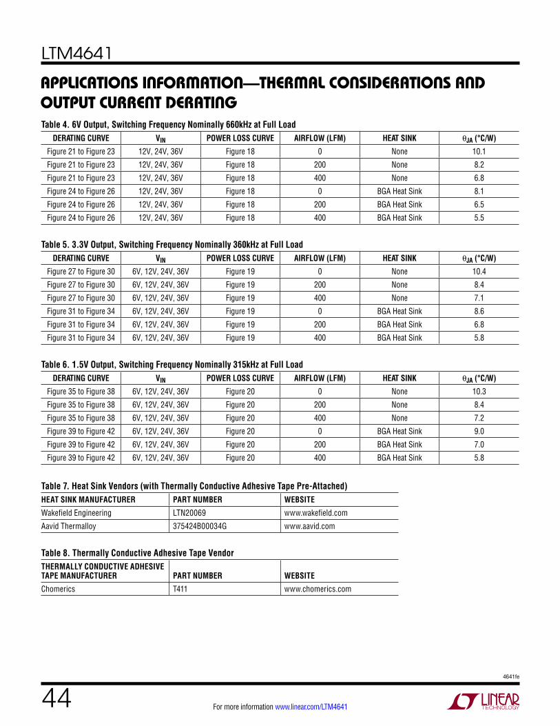
LTM4641
444641fe
For more information www.linear.com/LTM4641
applicaTions inForMaTion—TherMal consiDeraTions anD ouTpuT currenT DeraTingTable 4. 6V Output, Switching Frequency Nominally 660kHz at Full Load
DERATING CURVE VIN POWER LOSS CURVE AIRFLOW (LFM) HEAT SINK θJA (°C/W)
Figure 21 to Figure 23 12V, 24V, 36V Figure 18 0 None 10.1
Figure 21 to Figure 23 12V, 24V, 36V Figure 18 200 None 8.2
Figure 21 to Figure 23 12V, 24V, 36V Figure 18 400 None 6.8
Figure 24 to Figure 26 12V, 24V, 36V Figure 18 0 BGA Heat Sink 8.1
Figure 24 to Figure 26 12V, 24V, 36V Figure 18 200 BGA Heat Sink 6.5
Figure 24 to Figure 26 12V, 24V, 36V Figure 18 400 BGA Heat Sink 5.5
Table 5. 3.3V Output, Switching Frequency Nominally 360kHz at Full LoadDERATING CURVE VIN POWER LOSS CURVE AIRFLOW (LFM) HEAT SINK θJA (°C/W)
Figure 27 to Figure 30 6V, 12V, 24V, 36V Figure 19 0 None 10.4
Figure 27 to Figure 30 6V, 12V, 24V, 36V Figure 19 200 None 8.4
Figure 27 to Figure 30 6V, 12V, 24V, 36V Figure 19 400 None 7.1
Figure 31 to Figure 34 6V, 12V, 24V, 36V Figure 19 0 BGA Heat Sink 8.6
Figure 31 to Figure 34 6V, 12V, 24V, 36V Figure 19 200 BGA Heat Sink 6.8
Figure 31 to Figure 34 6V, 12V, 24V, 36V Figure 19 400 BGA Heat Sink 5.8
Table 6. 1.5V Output, Switching Frequency Nominally 315kHz at Full LoadDERATING CURVE VIN POWER LOSS CURVE AIRFLOW (LFM) HEAT SINK θJA (°C/W)
Figure 35 to Figure 38 6V, 12V, 24V, 36V Figure 20 0 None 10.3
Figure 35 to Figure 38 6V, 12V, 24V, 36V Figure 20 200 None 8.4
Figure 35 to Figure 38 6V, 12V, 24V, 36V Figure 20 400 None 7.2
Figure 39 to Figure 42 6V, 12V, 24V, 36V Figure 20 0 BGA Heat Sink 9.0
Figure 39 to Figure 42 6V, 12V, 24V, 36V Figure 20 200 BGA Heat Sink 7.0
Figure 39 to Figure 42 6V, 12V, 24V, 36V Figure 20 400 BGA Heat Sink 5.8
Table 7. Heat Sink Vendors (with Thermally Conductive Adhesive Tape Pre-Attached)HEAT SINK MANUFACTURER PART NUMBER WEBSITE
Wakefield Engineering LTN20069 www.wakefield.com
Aavid Thermalloy 375424B00034G www.aavid.com
Table 8. Thermally Conductive Adhesive Tape VendorTHERMALLY CONDUCTIVE ADHESIVE TAPE MANUFACTURER PART NUMBER WEBSITE
Chomerics T411 www.chomerics.com

LTM4641
454641fe
For more information www.linear.com/LTM4641
applicaTions inForMaTion—ouTpuT capaciTance TableTable 9. Transient Performance (Typical Values) vs Recommended Output Capacitance. Figure 45 and Figure 46 Circuits
COUT(MLCC) COUT(BULK)
VOUT VENDOR PART NUMBER VENDOR PART NUMBER
≤ 3.3V AVX 12106D107MAT2A (100µF, 6.3V, 1210 Case Size) 12066D226MAT2A (22µF, 6.3V, 1206 Case Size)
Sanyo POSCAP 6TPE680MI (680µF, 6.3V, 18mΩ ESR, D4 Case Size)
Taiyo Yuden JMK325BJ107MM-T (100µF, 6.3V, 1210 Case Size) JMK316BJ226ML-T (22µF, 6.3V, 1206 Case Size)
TDK C3225X5R0J107MT (100µF, 6.3V, 1210 Case Size) C3216X5R0J226MT (22µF, 6.3V, 1206 Case Size)
> 3.3V AVX 1206YD226MAT2A (22µF, 16V, 1206 Case Size) Sanyo POSCAP 10TPF150ML (150µF, 10V, 15mΩ ESR, D3L Case Size)
Taiyo Yuden LMK316BJ476ML-T (47µF, 10V, 1206 Case Size) EMK316BJ226ML-T (22µF, 16V, 1206 Case Size)
TDK C3216X5R1A476M (47µF, 10V, 1206 Case Size) C3216X5R1C226M (22µF, 16V, 1206 Case Size)
VOUT (V) VIN (V)
RfSET (MΩ)
RSET1A, RSET1B (kΩ)
RSET2 (kΩ)
CIN (CERAMIC)
CIN* (BULK)
COUT2 (CERAMIC)
COUT1 (BULK)
CFFA, CFFB
LOAD STEP SLEW RATE (A/µs)
TRANSIENT DROOP, 0A TO 5A LOAD STEP (mV)
TRANSIENT, PEAK-TO-PEAK, 0A TO 5A TO 0A STEP (mVPK-PK)
RECOVERY TIME (µs)
0.9 5, 12, 24, 36 0.931 4.12 – 2 × 10µF 100µF 3 × 22µF 680µF – 5 60 130 25
0.9 5, 12, 24, 36 0.931 4.12 – 2 × 10µF 100µF 4 × 100µF – – 5 60 140 25
1 5, 12, 24, 36 1.00 5.49 – 2 × 10µF 100µF 3 × 22µF 680µF – 5 65 135 25
1 5, 12, 24, 36 1.00 5.49 – 2 × 10µF 100µF 4 × 100µF – – 5 70 150 25
1.2 5, 12, 24, 36 1.13 8.2 – 2 × 10µF 100µF 3 × 22µF 680µF – 5 70 140 25
1.2 5, 12, 24, 36 1.13 8.2 – 2 × 10µF 100µF 4 × 100µF – – 5 80 170 30
1.5 5, 12, 24, 36 1.43 8.2 33.2 2 × 10µF 100µF 3 × 22µF 680µF – 5 75 155 30
1.5 5, 12, 24, 36 1.43 8.2 33.2 2 × 10µF 100µF 4 × 100µF – 220pF 5 90 190 30
1.8 5, 12, 24, 36 2.00 8.2 16.5 2 × 10µF 100µF 3 × 22µF 680µF – 5 80 170 40
1.8 5, 12, 24, 36 2.00 8.2 16.5 2 × 10µF 100µF 3 × 100µF – 220pF 5 100 215 30
2.5 5, 12, 24, 36 5.76 8.2 7.5 2 × 10µF 100µF 3 × 22µF 680µF – 5 100 230 50
2.5 5, 12, 24, 36 5.76 8.2 7.5 2 × 10µF 100µF 3 × 100µF – 220pF 5 140 290 30
3.3 5, 12, 24, 36 – 8.2 4.7 2 × 10µF 100µF 3 × 22µF 680µF – 5 140 275 60
3.3 5, 12, 24, 36 – 8.2 4.7 2 × 10µF 100µF 3 × 100µF – 100pF 5 200 420 30
5 12, 24, 36 – 8.2 2.61 2 × 10µF 100µF 2 × 22µF 150µF 220pF 5 220 450 50
5 12, 24, 36 – 8.2 2.61 2 × 10µF 100µF 3 × 47µF – 100pF 5 250 570 30
6 12, 24, 36 – 8.2 2.05 2 × 10µF 100µF 2 × 22µF 150µF 220pF 5 240 500 55
6 12, 24, 36 – 8.2 2.05 2 × 10µF 100µF 3 × 47µF – 100pF 5 300 660 30
*Bulk Capacitance is optional if VIN has very low input impedance.
LTM4641
464641fe
For more information www.linear.com/LTM4641
applicaTions inForMaTion—saFeTy anD layouT guiDanceSafety Considerations
The LTM4641 modules do not provide galvanic isolation from VIN to VOUT. There is no internal fuse. If fusing is required, a slow blow fuse with a rating twice the maximum input current needs to be provided. The LTM4641 sup-ports overcurrent protection and two kinds of overvoltage protection (see the Power Good Indicator and Latching Output Overvoltage Protection section).
Layout Checklist/Example
The high integration of LTM4641 makes the PCB board layout very straightforward. To optimize its electrical and thermal performance, some layout considerations are necessary. Figure 43 and Figure 44 show recommended layouts for the circuits shown in Figure 45 and Figure 46, respectively.
• Refer to the following document for device land pattern and stencil design: http://www.linear.com/docs/40146.
• The gerber file for demo board DC1543 can be down-loaded at http://www.linear.com/demo
• Use a solid copper GND plane directly underneath the module. This will help form the return path electrical connections to the input source and output load. It will also provide a thermal path for removing heat from the BGA package and minimize junction temperature rise of the LTM4641 for a given application. For consistent ripple and noise from application to application, connect the output GND plane (the one that conducts load side return current back to the module) and the input GND plane (the one that conducts module return current back to the input source) underneath the module, only.
• Use large PCB copper areas for high current paths, including VINH and VOUT.
• Place high frequency ceramic input and output capaci-tors next to the VINH, GND and VOUT pins to minimize high frequency noise. VINH exception: If MSP is used, (1) place MSP as close to the VINH pins of the LTM4641 as possible and (2) bypass the drain of MSP—and not VINH—to GND pins of the LTM4641. Only one or two high frequency MLCCs (COUT(MLCC)) need be placed directly next to the VOUT and GND pins of the LTM4641, to minimize high frequency noise close to the source.
The majority of COUT(MLCC) should be located close to the load to provide high quality bypassing.
• To minimize the via conduction loss and reduce module thermal stress, use multiple vias for interconnection between top layer and other power layers.
• Do not put vias directly under any pads, unless they are capped or plated over.
• Use a separated SGND ground copper area for compo-nents connecting to signal pins. Components connecting to SGND should be placed as close to the module as possible and routed with minimum trace lengths and trace widths, for best noise immunity.
• Note that there are two clusters of SGND pins on the module: one, formed by Pins A1-A3, B1-B3, C1-C4 (A1-quadrant); and a second formed by Pins K1, K3, L3, and M1-M3 (M1-quadrant). It is good PCB design practice to provide a copper plane connecting all A1-quadrant SGND pins together and another plane connecting all M1-quadrant SGND pins together. It is not necessary to connect these two clusters of SGND copper planes to each other in the PCB layout, because all SGND pins are electrically connected to each other internal to the module.
• Do not connect the any SGND pins or SGND plane(s) to the GND plane; the electrical star connection is made internal to the module.
• For parallel module operation, see the Multimodule Parallel Operation section for a list of interconnecting pins across paralleled modules. Circuit Figures 56 and 66 show four and two LTM4641 devices operating in parallel, respectively. Route signal-level (non-power) nets on an internal layer, with GND planes overlapping signal routes to shield them from noise. It is even more effective to surround module-to-module signal connections on the internal layer containing the signal routes with adjacent GND planes or routes, and periodi-cally “punching-through” GND via connections to GND plane shields on adjacent layers. This practice forms the equivalent of a “coaxial cable” structure within the PCB, and is highly effective at shielding sensitive signals from noise sources. Maintain differential routing of the VOSNS
+/VOSNS– pin pair.

LTM4641
474641fe
For more information www.linear.com/LTM4641
applicaTions inForMaTion—saFeTy anD layouT guiDance• Place all feedback components as close to the module
as possible, giving layout priority first to capacitors CFFA, CFFB, CCMA, CCMB and CDM (if used)—followed next by RSET1A, RSET1B and RSET2 (if used). See Figure 5 in the Applications Information section and Figure 64 in Appendix D for more details. Maintain differential routing of the remote-sense lines between the load and the module. Form a “coaxial cable” structure that surrounds the remote-sense lines with GND potential within the PCB, to the extent that layout permits. See
an example of routing the VOUT/GND remote-sense pin pair in Layer 3 of DC1543.
• To facilitate stuffing verification, and test and debug ac-tivities, consider routing control signals of the LTM4641 with short traces to localized test points, test pads or test vias—as PCB layout space permits. Both in-house and contract manufacturers enjoy gaining electrical access to all non low impedance (≥10Ω) pins of an IC or μModule regulator to improve in-circuit test (ICT) coverage.
Figure 43. Recommended PCB Layout, Figure 45 Circuit. View of the LTM4641 from Top of Package
Figure 44. Recommended PCB Layout, Figure 46 Circuit. View of the LTM4641 from Top of Package

LTM4641
484641fe
For more information www.linear.com/LTM4641
Typical applicaTions
+
RSET216.4k
4641 F45
RfSET2M
COUT(MLCC)47µF10V×6
CIN(MLCC)10µF50V×2
CIN(BULK)50V
VIN4V TO 38V
(4.5V START-UP)
VOUT1.8V10A
LOCAL HIGHFREQUENCYDECOUPLING
RSET1A8.2k
RSET1B8.2k LOAD
VOSNS+
VOUTVINL
fSET
INTVCCDRVCC
IOVRETRYOVLO
RUN
VOSNS–
VORB+
UVLOHYSTFCB
GNDSGNDCOMPTMR
CSS4.7nF
TRACK/SS
VING VINGP SWVINH
LTM4641
CROWBAR
LATCH
VORB–
TEMP1VREF
OVPGMOTBH
PGOOD
CTMRN/U
SGND CONNECTS TO GND INTERNAL TO MODULE. KEEP SGNDROUTES/PLANES SEPARATE FROM GND ON MOTHERBOARD
Figure 45. 4VIN to 38VIN, LTM4641 Basic Configuration, 1.8V Output at 10A
+
RSET24.7k
MCB: NXP PSMN5R0-30YLMSP: NXP PSMN7R0-60YS
MCB
MSP
4641 F46
CIN(MLCC)10µF50V×2
100µF6.3V×3
CIN(BULK)100µF50V
4.5V START-UPOPERATION
UP TO 38VIN
VOUT3.3V10A
LOCAL HIGHFREQUENCYDECOUPLING
RSET1A8.2k
CFFA100pF
CFFB100pF
RSET1B8.2k LOAD
VOSNS+
VOUTVINL
fSET
INTVCCDRVCC
IOVRETRYOVLO
RUN
VOSNS–
VORB+
UVLOHYSTFCB
GNDSGNDCOMPTMR
CSS22nF
TRACK/SS
VING VINGP SWVINH
LTM4641
CROWBAR
LATCH
VORB–
TEMP1VREF
OVPGMOTBH
PGOOD
SGND CONNECTS TO GND INTERNAL TO MODULE. KEEP SGNDROUTES/PLANES SEPARATE FROM GND ON MOTHERBOARD
Figure 46. LTM4641 Delivering 3.3V Output at 10A, and Providing Robust Output Overvoltage Protection from up to 38VIN. Dropout Operation May Occur Below 4.8VIN. See Figure 11 to Implement Custom UVLO Rising/Falling Settings to Avoid Dropout Operation
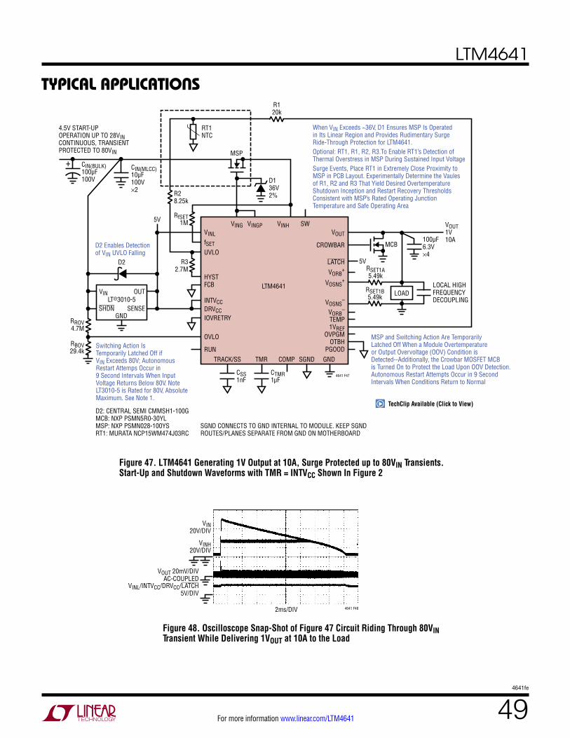
LTM4641
494641fe
For more information www.linear.com/LTM4641
Typical applicaTions
Figure 47. LTM4641 Generating 1V Output at 10A, Surge Protected up to 80VIN Transients.Start-Up and Shutdown Waveforms with TMR = INTVCC Shown In Figure 2
Figure 48. Oscilloscope Snap-Shot of Figure 47 Circuit Riding Through 80VIN Transient While Delivering 1VOUT at 10A to the Load
VIN20V/DIV
VINH20V/DIV
2ms/DIV 4641 F48
VOUT 20mV/DIVAC-COUPLED
VINL/INTVCC/DRVCC/LATCH5V/DIV
4.5V START-UPOPERATION UP TO 28VIN CONTINUOUS, TRANSIENT PROTECTED TO 80VIN
+
MCB
5V
D136V2%R2
8.25k
MSP
R120k
RT1NTC
4641 F47
CIN(MLCC)10µF100V×2
100µF6.3V×4
CIN(BULK)100µF100V
VOUT1V10A
LOCAL HIGHFREQUENCYDECOUPLING
RSET1A5.49k
RSET1B5.49k LOAD
VOSNS+
VOUTVINLfSET
UVLO
HYSTFCB
INTVCCDRVCCIOVRETRY
OVLO
RUN
VOSNS–
VORB+
GNDSGNDCOMPTMR
CSS1nF
TRACK/SS
VING
RfSET1M
R32.7M
VINGP5V
SWVINH
LTM4641
CROWBAR
LATCH
VORB–
TEMP1VREF
OVPGMOTBH
PGOOD
CTMR1µF
SENSE
RBOV29.4k
Switching Action Is Temporarily Latched Off if VIN Exceeds 80V; Autonomous Restart Attemps Occur in 9 Second Intervals When Input Voltage Returns Below 80V. NoteLT3010-5 is Rated for 80V, Absolute Maximum. See Note 1.
D2 Enables Detectionof VIN UVLO Falling
MSP and Switching Action Are TemporarilyLatched Off When a Module Overtemperature or Output Overvoltage (OOV) Condition is Detected--Additionally, the Crowbar MOSFET MCB is Turned On to Protect the Load Upon OOV Detection. Autonomous Restart Attempts Occur in 9 Second Intervals When Conditions Return to Normal
When VIN Exceeds ~36V, D1 Ensures MSP Is Operated in Its Linear Region and Provides Rudimentary Surge Ride-Through Protection for LTM4641. Optional: RT1, R1, R2, R3.To Enable RT1’s Detection of Thermal Overstress in MSP During Sustained Input Voltage Surge Events, Place RT1 in Extremely Close Proximity to MSP in PCB Layout. Experimentally Determine the Vaules of R1, R2 and R3 That Yield Desired Overtemperature Shutdown Inception and Restart Recovery Thresholds Consistent with MSP’s Rated Operating Junction Temperature and Safe Operating Area
RROV4.7M
OUTVIN
GND
LT®3010-5
D2
SHDN
D2: CENTRAL SEMI CMMSH1-100GMCB: NXP PSMN5R0-30YLMSP: NXP PSMN028-100YSRT1: MURATA NCP15WM474J03RC
SGND CONNECTS TO GND INTERNAL TO MODULE. KEEP SGNDROUTES/PLANES SEPARATE FROM GND ON MOTHERBOARD
TechClip Available (Click to View)

LTM4641
504641fe
For more information www.linear.com/LTM4641
Typical applicaTions
Figure 49. LTM4641 Producing 0.9VOUT at 10A, from 3.3VIN, and Providing Advanced Output Overvoltage Protection. VINL, INTVCC, and DRVCC Biased from a Low Power Auxiliary 5V Rail
Figure 50. Oscilloscope Snap-Shot of Figure 49 Circuit, 2Ω Load on VOUT. 3.3VIN Applied Briefly to Highlight UVLO Rising and Falling Thresholds
VIN1V/DIV
VOUT1V/DIV
HYST5V/DIV
PGOOD5V/DIV
4ms/DIV 4641 F50
+
MCB: NXP PH2625LMSP: NXP PSMN013-30LL
MCB
MSP
4641 F49
CIN(MLCC)47µF6.3V×2
100µF6.3V×4
CIN(BULK)
3.3VIN NOMINAL3VIN RISING START-UP
2.3VIN FALLING SHUTDOWN
5VLOW POWER BIAS
<50mA PEAK
VOUT0.9V10A
LOCAL HIGHFREQUENCYDECOUPLING
RSET1A4.12k
RSET1B4.12k
RfSET360k
RHYST1M
RBUV30.9k
100k
RTUV150k
LOAD
VOSNS+
VOUTVINL
fSET
INTVCCDRVCCIOVRETRYOVLO
RUN
VOSNS–
VORB+
FCBHYST
UVLO
GNDSGNDCOMPTMR
CSS4.7nF
TRACK/SS
VING VINGP SWVINH
LTM4641
CROWBAR
LATCH
VORB–
TEMP1VREF
OVPGMOTBH
PGOOD
SGND CONNECTS TO GND INTERNAL TO MODULE, KEEP SGNDROUTES/PLANES SEPARATE FROM GND ON MOTHERBOARD

LTM4641
514641fe
For more information www.linear.com/LTM4641
Typical applicaTions
Figure 51. Over-Driving INTVCC/DRVCC to Reduce VINL-to-INTVCC Linear Regulator Losses (cf. Figures 52 to 54)
Figure 52. Thermal Image of U1 from Figure 51 Circuit. Delivering 5VOUT at 10A from 36VIN, with INTVCC Connected to DRVCC and D1c = Open and D2 = Open. TA = 25°C, Bench Testing, No Airflow
Figure 53. Thermal Image of U1 from Figure 51 Circuit. Delivering 6VOUT at 10A from 36VIN, with INTVCC Connected to DRVCC and D1c = Open and D2 = Open. TA = 25°C, Bench Testing, No Airflow
Figure 54. Thermal Image of U1 from Figure 51 Circuit. Delivering 5VOUT at 10A from 36VIN, with 5VOUT Feeding INTVCC/DRVCC Through D1c Diode. TA = 25°C, Bench Testing, No Airflow
Figure 55. Thermal Image of U1 from Figure 51 Circuit. Delivering 6VOUT at 10A from 36VIN, with 6VOUT Feeding INTVCC/DRVCC Through D1c Diode. TA = 25°C, Bench Testing, No Airflow
+
RSET2~2.05k TO 2.61k
4641 F51
CIN(MLCC)10µF50V×2
VIN8.5V TO 38V
(10V START-UP)
CVINL0.1µF
50V
CDRVCC2.2µF
COUT(MLCC)47µF10V×2
COUT(BULK)150µF10V
LDO Losses in the LTM4641 Can Be Greatly Reduced When an Auxilliary ~5V to 6V Source (VAUX) Is Available toDrive DRVCC Through a Schottky Diode as Shown (D1c). When LTM4641 Is Configured to Produce ~5VOUT to 6VOUT,its Output Can Be VAUX. Provide a Current Path to VINL from VIN and INTVCC/DRVCC Whenever Overdriving INTVCC/DRVCCwith VAUX–Accomplished Here with D1a and D1b
CIN(BULK)
~5VOUTTO 6VOUTUP TO 10A
RSET1A8.2k
RSET1B8.2k
RHYST1M
RBUV15.8k
RTUV294k
LOAD
VOSNS+
VOUTVINL
a
D1
D2
D1, D2: CENTRAL SEMI CMKSH2-4LR SOT-363 PACKAGE
c
b
VAUX
fSET
INTVCCDRVCCIOVRETRYOVLO
RUN
VOSNS–
VORB+
FCBHYST
UVLO
GNDSGNDCOMPTMR
CSS47nF
TRACK/SS
VING VINGP SWVINH
LTM4641
CROWBAR
LATCH
VORB–
TEMP1VREF
OVPGMOTBH
PGOOD
SGND CONNECTS TO GND INTERNAL TO MODULE, KEEP SGNDROUTES/PLANES SEPARATE FROM GND ON MOTHERBOARD

LTM4641
524641fe
For more information www.linear.com/LTM4641
Typical applicaTions
Figure 56: 1V, 40A Fault-Protected Load Powered by Four Parallel LTM4641—from Up to 38VIN. cf. Figure 57
RfSET1750k
4.5VIN START-UPOPERATION UP TO 38VAND DOWN TO 4V
CMLCC(OUT)100µF6.3V×12
CIN(MLCC)10µF50V×4
CIN(BULK)100µF50V×2
VOUT1V40A
LOCAL HIGHFREQUENCYDECOUPLING
RSET1A1.37k
CFF1100pF
CFF2100pF
RSET1B1.37k LOAD
VOSNS+
VOUTVINL
fSET
INTVCCDRVCC
IOVRETRYOVLO
RUNRUN ENABLE
LATCHOFF RESET
PULL LATCH NORMALLY LOW FORLATCHOFF RESPONSE TO OUTPUTOVERVOLTAGE AND OVER-TEMPERATURE EVENTS. PULLLATCH HIGH TO RESTART 1V OUTPUT
ALTERNATIVELY, CONNECT LATCHTO INTVCC AND INSTALL CTMR1,CTMR2, CTMR3 AND CTMR4 TO SET 1V OUTPUT FOR TIMEDAUTONOMOUS RESTART AFTERFAULT SHUTDOWN EVENTS
MCB: NXP PSMN5R0-30YLMSP: NXP PSMN3R0-60BS
FAULT INDICATORCSS
22nFCTMR1
N/U
VOSNS–
VORB+
UVLOHYSTFCB
GNDSGNDCOMPTMRTRACK/SS
VING VINGP
MSP
MCB
VINH
U1LTM4641
CROWBAR
LATCH
VORB–
TEMP1VREF
OVPGMOTBH
PGOOD
1
1
11
1
1
SW
CDM110pF
RfSET2750k
VOSNS+
VOUTVINL
fSET
INTVCCDRVCC
IOVRETRYOVLO
RUN
CTMR2N/U
VOSNS–
VORB+
UVLOHYSTFCB
GNDSGNDCOMPTMRTRACK/SS
VING VINGP VINH
U2LTM4641
CROWBAR
LATCH
VORB–
TEMP1VREF
OVPGMOTBH
PGOOD
2
2
2
2
2
SW
CDM210pF
TO SYSTEM µP(OPTIONAL)
RfSET3750k
VOSNS+
VOUTVINL
fSET
INTVCCDRVCC
IOVRETRYOVLO
RUN
CTMR3N/U
VOSNS–
VORB+
UVLOHYSTFCB
GNDSGNDCOMPTMRTRACK/SS
VING VINGP VINH
U3LTM4641
CROWBAR
LATCH
VORB–
TEMP1VREF
OVPGMOTBH
PGOOD
3
3
3
3
3
SW
CDM310pF
RfSET4750k
VOSNS+
VOUTVINL
fSET
INTVCCDRVCC
IOVRETRYOVLO
RUN
CTMR4N/U
VOSNS–
VORB+
UVLOHYSTFCB
GNDSGNDCOMPTMRTRACK/SS
VING VINGP VINH
U4LTM4641
CROWBAR
LATCH
VORB–
TEMP1VREF
OVPGMOTBH
PGOOD
4
4
4641 F564
4
4
SW
CDM410pF
U1, U2, U3 AND U4 SGND ( 1, 2, 3, 4) CONNECT TO GND INTERNAL TO THEIR RESPECTIVE MODULES. KEEP MODULE SGND ROUTES/PLANES SEPARATE FROM OTHER MODULES AND FROM GND ON MOTHERBOARD

LTM4641
534641fe
For more information www.linear.com/LTM4641
Typical applicaTions
Figure 57: Current-Sharing Performance of Four Paralleled LTM4641. Figure 56 Circuit, Operating at 28VIN
TOTAL OUTPUT CURRENT (A)0
8
10
12
32
4641 F57
6
MOD
ULE
OUTP
UT C
URRE
NT (A
)
4
8 16 24 40
2
0
–2
U1 OUTPUT CURRENTU2 OUTPUT CURRENTU3 OUTPUT CURRENTU4 OUTPUT CURRENT
Figure 58. Negative Output Application. Delivering –5.2VOUT at Up to 10A, from Up to 32.8VIN. cf. Figure 59
CIN(MLCC)10µF50V×4
COUT(MLCC)47µF10V×4
CIN(BULK)50V
OPERATIONUP TO 32.8VIN4.5V START-UP
LOCAL HIGHFREQUENCYDECOUPLING
FOR MORE INFORMATION ABOUT CONFIGURING STEP-DOWN BUCK CONVERTERS AS BUCK-BOOST CONVERTERS, FOR GENERATING NEGATIVE VOUT, SEE http://www.linear.com/docs/39881
RSET1A8.2k
RSET1B8.2k
LOAD
VOSNS+
VOUTVINL
fSET
INTVCCDRVCC
IOVRETRYOVLO
RUN
CSS10nF
VOSNS–
VORB+
UVLOHYSTFCB
GNDSGNDCOMPTMRTRACK/SS
VING VINGP VINH
U1LTM4641
CROWBAR
LATCH
VORB–
TEMP1VREF
OVPGMOTBH
PGOOD
SW
RSET22.46k
100k
D1: CENTRAL SEMI CMPSH1-4LE SGND CONNECTS TO GND INTERNAL TO MODULE, KEEP SGNDROUTES/PLANES SEPARATE FROM GND ON MOTHERBOARD
D1
VOUT–5.2V ATUP TO 10A
4641 F58
+

LTM4641
544641fe
For more information www.linear.com/LTM4641
Typical applicaTions
Figure 60. Fault-Protected Load with Power Supply Management. LTM4641’s Fast Output Overvoltage Latchoff TripThreshold Remains Consistently 11% Above LTC2978-Commanded Target VOUT, Even as VOUT is Margined Via I2C
RfSET1.13M 100µF
6.3V×4
CIN(MLCC)22µF25V×2
CIN(BULK)100µF25V
4.5V < VIN < 15V
ADDITIONALFAULT INDICATOR
VOUT1.2V NOMINALUP TO 10A OUTPUT
LOCAL HIGHFREQUENCYDECOUPLING
MSP: NXP PSMN017-30LLMCB: NXP PSMN5R0-30YL
LTM4641 SGND CONNECTS TO GND INTERNAL TO MODULE.KEEP SGND ROUTES/PLANES SEPARATE FROM GND ON MOTHERBOARD
RSET1A8.2k
RSET1B8.2k
R3035.7k
LOAD
VOSNS+
VOUTVINL
fSET
INTVCCDRVCC
IOVRETRYOVLO
RUN
CSS4.7nF
*
ONLY ONE OF EIGHT LTC2978 CHANNELS SHOWN. LTC2978 PULL-UPS,BYPASSING COMPONENTS, AND SOME PINS NOT SHOWN. FOR DETAILSOF LTC2978 IMPLEMENTATION, SEE LTC2978 DATA SHEET
**
LTC2978 MAY BE POWERED FROM EITHER AN EXTERNAL 3.3VSUPPLY OR THE SYSTEM BUS
†
VOSNS–
VORB+
UVLOHYSTFCB
GNDSGNDCOMPTMRTRACK/SS
VING VINGP
MSP
MCB
LATCHOFFRESET
VINH
LTM4641*
CROWBAR
LATCH
VORB–
TEMP1VREF
OVPGMOTBH
PGOOD
SW
VDD33
VIN_EN
WP
SDASCLALERTCONTROL0
3.3V†
WRITE PROTECT
TO UPSTREAMSYSTEM ENABLE
PMBusINTERFACE
VOUT_EN0
PWRGDWDI/RESET WATCHDOG TIMER INTERRUPT
TO µP RESET INPUT
VDACPOVSENSEPOVSENSEMO
VDACMO
VIN_SNSVPWR
ASEL1GND ASELO
LTC2978**
FAULTOOSHARE_CLK
TO/FROMOTHER
LTC2978s
+
Figure 59. Pulsed Application of VIN. Figure 58 Circuit with 500Ω Load.*Ultralow VF of D1 Minimizes VOUT Overshoot Upon Energization
VIN 10V/DIV
HYST 2V/DIVPGOOD 2V/DIV
VOUT 2V/DIV
20ms/DIV 4641 F59
*

LTM4641
554641fe
For more information www.linear.com/LTM4641
Typical applicaTions
Figure 61. LTM4641’s VOUT Margined High/Low by LTC2978 Via I2C Commands. Figure 60 Circuit. 12VIN.VOUT_COMMAND (0x21) = 1.20V, VOUT_MARGIN_HIGH (0x25) = 1.32V, VOUT_MARGIN_LOW (0x26) = 1.08V
VOUT200mV/DIV
VDACPO500mV/DIV
SDA, SCL2V/DIV
20ms/DIV 4641 F61a
VOUT200mV/DIV
VDACPO500mV/DIVSDA, SCL2V/DIV
20ms/DIV 4641 F61b
VOUT200mV/DIV
VDACPO500mV/DIV
SDA, SCL2V/DIV
20ms/DIV 4641 F61c
VOUT200mV/DIV
VDACPO500mV/DIVSDA, SCL2V/DIV
20ms/DIV 4641 F61d
(61a) PMBus OPERATION (Reg. 0x01): 0x80 → 0xA8 (Margin High) (61b) PMBus OPERATION (Reg. 0x01): 0xA8 → 0x80 (Margin Off)
(61c) PMBus OPERATION (Reg. 0x01): 0x80 → 0x98 (Margin Low) (61d) PMBus OPERATION (Reg. 0x01): 0x98 → 0x80 (Margin Off)
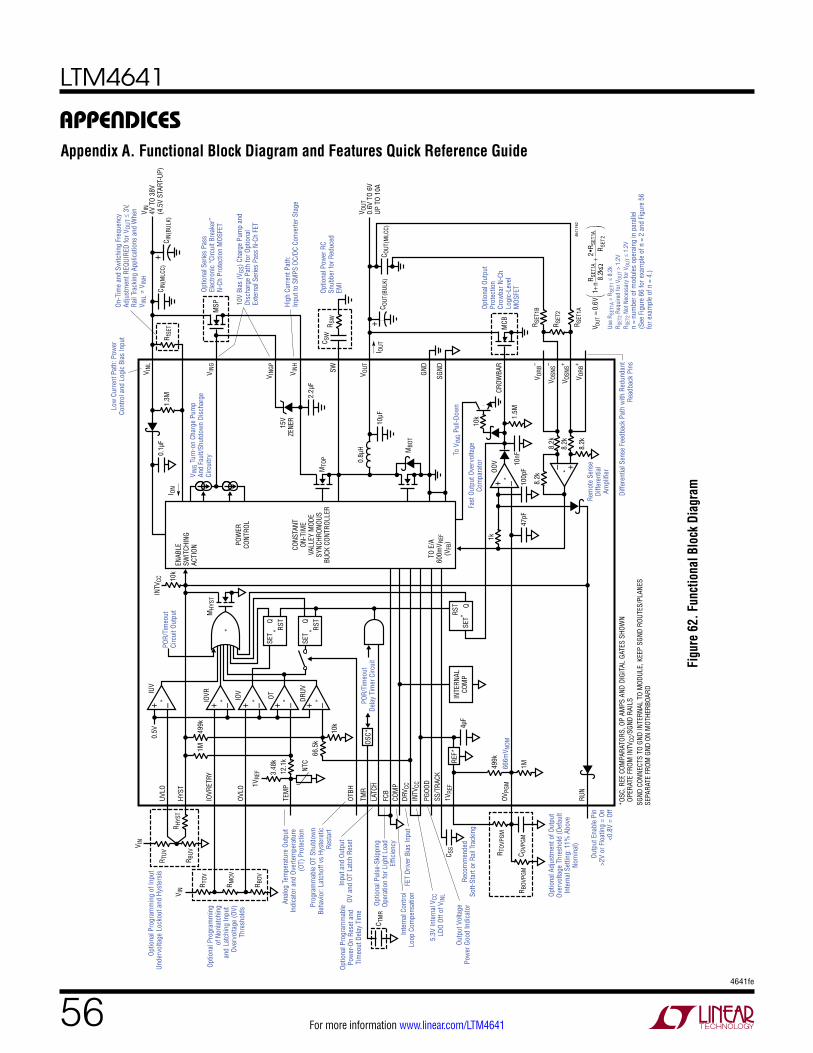
LTM4641
564641fe
For more information www.linear.com/LTM4641
appenDicesAppendix A. Functional Block Diagram and Features Quick Reference Guide
Figu
re 6
2. F
unct
iona
l Blo
ck D
iagr
am
MHY
ST
0.5V
IUV
IOVR
10k
499k
10k
3.48
k
NTC
TEM
P
OTBH
TMR
LATC
H
OVLO
IOVR
ETRY
HYST
UVLO
R HYS
T
66.5
k
1VRE
F 12.1
k
1M
R TUV
R TOV
R MOV
R BOV
V IN
V IN
R BUV
INTV
CCPO
R/Ti
meo
utCi
rcui
t Out
put
Optio
nal P
rogr
amm
ing
of In
put
Unde
rvol
tage
Loc
kout
and
Hys
ters
is
Optio
nal P
rogr
amm
ing
of N
onla
tchi
ngan
d La
tchi
ng In
put
Over
volta
ge (O
V)Th
resh
olds
Anal
og T
empe
ratu
re O
utpu
tIn
dica
tor a
nd O
verte
mpe
ratu
re(O
T) P
rote
ctio
n
Optio
nal P
rogr
amm
able
Pow
er-O
n Re
set a
ndTi
meo
ut D
elay
Tim
e
Inpu
t and
Out
put
OV a
nd O
T La
tch
Rese
t
Inte
rnal
Con
trol
Loop
Com
pens
atio
n
5.3V
Inte
rnal
VCC
LDO
Off o
f VIN
L
Outp
ut V
olta
gePo
wer
Goo
d In
dica
tor
FET
Driv
er B
ias
Inpu
t
Outp
ut E
nabl
e Pi
n>2
V or
Flo
atin
g =
On<0
.8V
= Of
f
Reco
mm
ende
d So
ft-St
art o
r Rai
l Tra
ckin
g
Optio
nal A
djus
tmen
t of O
utpu
tOv
ervo
ltage
Thr
esho
ld (D
efau
ltIn
tern
al S
ettin
g: 1
1% A
bove
Nom
inal
)
Optio
nal P
ulse
-Ski
ppin
gOp
erat
ion
for L
ight
Loa
dEf
ficie
ncy
Prog
ram
mab
le O
T Sh
utdo
wn
Beha
vior
: Lat
chof
f vs
Hyst
eret
icRe
star
t
POR/
Tim
eout
Dela
y Ti
mer
Circ
uit
Fast
Out
put O
verv
olta
geCo
mpa
rato
r
Rem
ote
Sens
eDi
ffere
ntia
lAm
plifi
er
Optio
nal O
utpu
tPr
otec
tion
Crow
bar N
-Ch
Logi
c-Le
vel
MOS
FETOp
tiona
l Pow
er R
CSn
ubbe
r for
Red
uced
EMI
High
Cur
rent
Pat
h:In
put t
o SM
PS D
C/DC
Con
verte
r Sta
ge
Optio
nal S
erie
s Pa
ssEl
ectro
nic
“Circ
uit B
reak
er”
N-Ch
Pro
tect
ion
MOS
FET
Low
Cur
rent
Pat
h: P
ower
Cont
rol a
nd L
ogic
Bia
s In
put
On-T
ime
and
Switc
hing
Fre
quen
cyAd
just
men
t REQ
UIRE
D fo
r VOU
T ≤
3V,
Rail
Trac
king
App
licat
ions
and
Whe
nV I
NL ≠
VIN
H
10V
Bias
(VGS
) Cha
rge
Pum
p an
dDi
scha
rge
Path
for O
ptio
nal
Exte
rnal
Ser
ies
Pass
N-C
h FE
T
Diffe
rent
ial S
ense
Fee
dbac
k Pa
th w
ith R
edun
dant
Read
back
Pin
s
666m
V NOM
To V
ING
Pull-
Dow
n
+ – + –IO
V+ –
OT+ –
DRUV
+ –
+ –
SET
Q
RST
SET
Q
RST
OSC*
REF*
FCB
COM
P
PGOO
DSS
/TRA
CK1V
REF
OVPG
M
RUN
C SS
DRV C
CIN
TVCC
C TM
R
4µF
SET
Q
RST
OOV
100p
F
MCB
1.5M
10nF
47pF
1k
INTE
RNAL
COM
P
499k
R TOV
PGM
R BOV
PGM
C OVP
GM
10k
R SW
C SW
8.2k
8.2k
V OSN
S–
V ORB
–
CROW
BAR
SGND
V ORB
+
V OSN
S+
R SET
1B
R SET
1A46
41 F
62
1M
*OSC
, REF
, COM
PARA
TORS
, OP
AMPS
AND
DIG
ITAL
GAT
ES S
HOW
N O
PERA
TE F
ROM
INTV
CC/S
GND
RAIL
SSG
ND C
ONNE
CTS
TO G
ND IN
TERN
AL T
O M
ODUL
E, K
EEP
SGND
ROU
TES/
PLAN
ESSE
PARA
TE F
ROM
GND
ON
MOT
HERB
OARD
ENAB
LESW
ITCH
ING
ACTI
ON
POW
ERCO
NTRO
L
TO E
/A60
0mV R
EF(V
FB)
CONS
TANT
ON-T
IME
VALL
EY M
ODE
SYNC
HRON
OUS
BUCK
CON
TROL
LER
8.2k
8.2k
R SET
2
+–
GND
SW
V OUT
V INH
V ING
P
V ING
V INL
15V
ZENE
R
I OUT
C OUT
(BUL
K)C O
UT(M
LCC)
V OUT
0.6V
TO
6VUP
TO
10A
V IN
4V T
O 38
V(4
.5V
STAR
T-UP
)
10µF
2.2µ
F
MTO
P
MBO
T
0.8µ
H
MSP
I ON
+
0.1µ
FC I
N(M
LCC)
C IN(
BULK
)1.
3M
V ING
Tur
n-on
Cha
rge
Pum
pAn
d Fa
ult/S
hutd
own
Disc
harg
eCi
rcui
try
R fSE
T
+
V OU
T=
0.6V
1+nR
SET1
A8.
2kΩ
+2•
RSE
T1A
RSE
T2
*
*
*****
* * *
*
Use
R SET
1A =
RSE
T1 ≤
8.2
kR S
ET2
Requ
ired
for V
OUT
> 1.
2VR S
ET2
Not N
eces
sary
for V
OUT
≤ 1.
2Vn
= nu
mbe
r of m
odul
es o
pera
ing
in p
aral
lel
(See
Fig
ure
66 fo
r exa
mpl
e of
n =
2 a
nd F
igur
e 56
fo
r exa
mpl
e of
n =
4.)

LTM4641
574641fe
For more information www.linear.com/LTM4641
appenDicesAppendix B. Start-Up/Shutdown State Diagram
Figu
re 6
3. S
tart-
Up/S
hutd
own
Stat
e Di
agra
m
LTM
4641
SHU
T DO
WN:
HOUS
EKEE
PING
AND
CONT
ROL
SECT
IONS
ARE
UNBI
ASED
; POW
ERST
AGE
IS O
FF; V
ING
ISDI
SCHA
RGED
INTV
CC >
2V,
NOM
INTV
CC <
2V,
NOM
INTV
CC <
2V,
NOM
INTV
CC >
2V,
NOM
AND
LATC
H =
LOW
TIM
EOUT
PER
IOD
BECO
MES
RES
ET
INTV
CC <
2V,
NOM
LTM
4641
HOU
SEKE
EPIN
GAL
IVE
AND
INHI
BITI
NGSW
ITCH
ING
ACTI
ON:
HYST
IS P
ULLE
D LO
W(M
HYST
IS O
N); P
OWER
STAG
E IS
OFF
; VIN
G IS
DISC
HARG
ED
LTM
4641
POW
ER S
TAGE
SWIT
CHIN
G AC
TION
IS O
N: M
HYST
IS O
FF;
V ING
IS C
HARG
E PU
MPE
DAB
OVE
V INH
; CON
TROL
LOOP
REG
ULAT
ES V
OUT
LTM
4641
LAT
CHOF
FCO
NDIT
ION
DETE
CTED
: HY
ST IS
LAT
CHED
LOW
(MHY
ST IS
ON)
; POW
ERST
AGE
IS O
FF; V
ING
ISDI
SCHA
RGED
LTM
4641
PRI
MED
TO
REGU
LATE
: WAI
TING
ONLY
FOR
RUN
PIN
TO
TRAN
SIST
ION
HIGH
AND
INTV
CC T
O EX
CEED
3.6
V NOM
;SW
ITCH
ING
ACTI
ON N
OTIN
HIBI
TED
BY H
OUSE
KEEP
ING
CIRC
UITR
Y (M
HYST
IS O
FF);
POW
ER S
TAGE
IS O
FF;
V ING
IS D
ISCH
ARGE
D
LTM
4641
VER
IFIC
ATIO
NOF
TIM
EOUT
PER
IOD
EXPI
RATI
ON: H
OUSE
KEEP
ING
CIRC
UITR
Y HO
LDS
HYST
LOW
(MHY
ST IS
ON)
UNT
IL A
ND
UNLE
SS T
HE U
VLO/
IOVR
ETRY
/OV
LO/C
ROW
BAR/
TEM
P/DR
V CC
MON
ITOR
OUT
PUTS
REM
AIN
CLEA
R FO
R TH
E FU
LL D
URAT
ION
OF T
HE T
IMEO
UT P
ERIO
D, A
S SE
T BY
TM
R PI
N (C
TMR)
; POW
ER
STAG
E IS
OFF
; VIN
G IS
DIS
CHAR
GED
INTV
CC >
2V,
NOM
;AN
D AN
Y OF
THE
FOL
LOW
ING
NONL
ATCH
ING
COND
ITON
S AP
PEAR
:1.
CUS
TOM
UVL
O IN
PUT
TOO
LOW
(VUL
VO <
UVO
V TH,
~0.
5VTH
)2.
NON
LATC
HING
INPU
T OV
ERVO
LTAG
E (V
IOVR
ETRY
> U
VOV T
H, ~
0.5V
TH)
3. D
RVCC
TOO
LOW
(VDR
VCC
< DR
V CC(
UVLO
_RIS
ING)
, ~3.
9VTH
)4.
NON
LATC
HING
OVE
RTEM
PERA
TURE
(O
TBH
= OP
EN C
IRCU
IT A
ND V
TEM
P <
OTTH
(REC
OVER
), ~5
14m
V TH)
AND
NO L
ATCH
OFF
FAUL
TS A
RE P
RESE
NT:
1. IN
PUT
VOLT
AGE
O.K.
(VOV
LO <
UVO
V TH,
~0.
5VTH
)2.
CRO
WBA
R O.
K. (V
CROW
BAR
< V C
ROW
BAR(
TH),
~1.5
V TH)
3. T
EMPE
RATU
RE O
.K.
(O
TBH
= LO
W A
ND V
TEM
P >
OTTH
(REC
OVER
), ~5
14m
V TH)
INTV
CC >
2V,
NOM
;AN
D AN
Y OF
THE
FOL
LOW
ING
NONL
ATCH
ING
COND
ITON
S AP
PEAR
:1.
CUS
TOM
UVL
O IN
PUT
TOO
LOW
(VUV
LO <
UVO
V TH,
~0.
5VTH
)2.
NON
LATC
HING
INPU
T OV
ERVO
LTAG
E (V
IOVR
ETRY
> U
VOV T
H, ~
0.5V
TH)
3. D
RVCC
TOO
LOW
(VDR
VCC
< DR
V CC(
UVLO
_FAL
LING
), ~3
.35V
TH)
4. N
ONLA
TCHI
NG O
VERT
EMPE
RATU
RE
(OTB
H =
OPEN
CIR
CUIT
AND
VTE
MP
< OT
TH(IN
CEPT
ION)
, ~43
8mV T
H)AN
D NO
LAT
CHOF
F FA
ULTS
ARE
PRE
SENT
:1.
INPU
T VO
LTAG
E O.
K. (V
OVLO
< U
VOV T
H, ~
0.5V
TH)
2. C
ROW
BAR
O.K.
(VCR
OWBA
R <
V CRO
WBA
R(TH
), ~1
.5V T
H)3.
TEM
PERA
TURE
O.K
.
(OTB
H =
LOW
AND
VTE
MP
> OT
TH(IN
CEPT
ION)
, ~43
8mV T
H)
INTV
CC >
2V,
NOM
;AN
D AL
L OF
THE
FOL
LOW
ING
FAUL
T FR
EE C
ONDI
TION
SAR
E PR
ESEN
T (O
R RE
CENT
LY A
PPEA
RED,
EXI
TING
LAT
CHOF
F):
1. C
USTO
M U
VLO
INPU
T O.
K. (V
UVLO
> U
VOV T
H, ~
0.5V
TH)
2. N
O IN
PUT
OVER
VOLT
AGE(
S)
(VIO
VRET
RY <
UVO
V TH
AND
V OVL
O <
UVOV
TH, ~
0.5V
TH)
3. C
ROW
BAR
INAC
TIVE
(VCR
OWBA
R <
V CRO
WBA
R(TH
), ~1
.5V T
H)4.
TEM
PERA
TURE
O.K
. (V T
EMP
> OT
TH(R
ECOV
ER),
~514
mV T
H)5.
DRV
CC A
BOVE
ITS
UVLO
(V
DRVC
C >
DRV C
C(UV
LO_R
ISIN
G), ~
4.05
V TH)
INTV
CC <
2V,
NOM
INTV
CC <
2V,
NOM
INTV
CC <
2V,
NOM
4641
F63
UVLO
/IOVR
ETRY
/OVL
O/CR
OWBA
R/TE
MP/
DRV C
C M
ONIT
OR
OUTP
UTS
HAVE
REM
AINE
D CL
EAR
FOR
THE
FULL
DUR
ATIO
N OF
THE
TIM
EOUT
PER
IOD
INTV
CC >
2V,
NOM
AND
LATC
H =
LOW
INTV
CC >
2V,
NOM
AND
ANY
OF T
HE F
OLLO
WIN
G LA
TCHO
FF F
AULT
S AR
E PR
ESEN
T:1.
LAT
CHOF
F IN
PUT
OVER
VOLT
AGE
(VOV
LO >
UVO
V TH,
~0.
5VTH
)2.
CRO
WBA
R AC
TIVE
(VCR
OWBA
R >
V CRO
WBA
R(TH
), ~1
.5V T
H)3.
LAT
CHOF
F OV
ERTE
MPE
RATU
RE
(OTB
H =
LOW
AND
VTE
MP
< OT
TH(IN
CEPT
ION)
, ~43
8mV T
H)
INTV
CC >
2V,
NOM
AND
ANY
LATC
HOFF
FAU
LTS
ARE
PRES
ENT:
1. L
ATCH
OFF
INPU
T OV
ERVO
LTAG
E (V
OVLO
> U
VOV T
H, ~
0.5V
TH)
2. C
ROW
BAR
ACTI
VE (V
CROW
BAR
> V C
ROW
BAR(
TH),
~1.5
V TH)
3. L
ATCH
OFF
OVER
TEM
PERA
TURE
(O
TBH
= LO
W A
ND V
TEM
P <
OTTH
(REC
OVER
), ~5
14m
V TH)
INTV
CC >
3.2
V, N
OMAN
D AL
L OF
THE
FOL
LOW
ING
FAUL
T FR
EE C
ONDI
TION
S AR
E PR
ESEN
T:1.
CUS
TOM
UVL
O IN
PUT
O.K.
(VUV
LO >
UVO
V TH,
~0.
5VTH
)2.
NO
INPU
T OV
ERVO
LTAG
E(S)
(V
IOVR
ETRY
< U
VOV T
H AN
D V O
VLO
< UV
OVTH
, ~0.
5VTH
)3.
CRO
WBA
R IN
ACTI
VE (V
CROW
BAR
< V C
ROW
BAR(
TH),
~1.5
V TH)
4. T
EMPE
RATU
RE O
.K. (
V TEM
P >
OTTH
(INCE
PTIO
N), ~
438m
V TH)
5. D
RVCC
ABO
VE IT
S UV
LO
(VDR
VCC
> DR
V CC(
UVLO
_FAL
LING
), ~3
.35V
TH)
6. R
UN >
VRU
N(ON
) (2V
TH, M
AX)
INTV
CC >
3.9
V, N
OMAN
D AL
L OF
THE
FOL
LOW
ING
FAUL
T FR
EE C
ONDI
TION
S AR
E PR
ESEN
T:1.
CUS
TOM
UVL
O IN
PUT
O.K.
(VUV
LO >
UVO
V TH,
~0.
5VTH
)2.
NO
INPU
T OV
ERVO
LTAG
E(S)
(V
IOVR
ETRY
< U
VOV T
H AN
D V O
VLO
< UV
OVTH
, ~0.
5VTH
)3.
CRO
WBA
R IN
ACTI
VE (V
CROW
BAR
< V C
ROW
BAR(
TH),
~1.5
V TH)
4. T
EMPE
RATU
RE O
.K. (
V TEM
P >
OTTH
(REC
OVER
), ~5
14m
V TH)
5. D
RVCC
ABO
VE IT
S UV
LO
(VDR
VCC
> DR
V CC(
UVLO
_RIS
ING)
, ~4.
05V T
H)6.
RUN
> V
RUN(
ON) (
2VTH
, MAX
)
EITH
ER IN
TVCC
> 3
.2V
NOM
AND
RUN
= L
OW (0
.8V T
H, M
IN)—
OR 2
V <
INTV
CC <
3.2
V, N
OM—
AND
ADD
ITIO
NALL
Y,
IN E
ITHE
R CA
SE, A
LL O
F TH
E FO
LLOW
ING
FAUL
T FR
EE
COND
ITIO
NS E
XIST
:1.
CUS
TOM
UVL
O IN
PUT
O.K.
(VUV
LO >
UVO
V TH,
~0.
5VTH
)2.
NO
INPU
T OV
ERVO
LTAG
E(S)
(V
IOVR
ETRY
< U
VOV T
H AN
D V O
VLO
< UV
OVTH
, ~0.
5VTH
)3.
CRO
WBA
R IN
ACTI
VE (V
CROW
BAR
< V C
ROW
BAR(
TH),
~1.5
V TH)
4. T
EMPE
RATU
RE O
.K. (
V TEM
P >
OTTH
(REC
OVER
), ~5
14m
V TH)
5. D
RVCC
ABO
VE IT
S UV
LO
(VDR
VCC
> DR
V CC(
UVLO
_FAL
LING
), ~3
.35V
TH)
LATC
HOFF
IS C
LEAR
ED W
HEN
INTV
CC >
2V,
NOM
AN
D LA
TCH
TOGG
LES
FROM
LOG
IC L
OW
TO H
IGH
AND
NO L
ATCH
OFF
FAUL
TS A
RE P
RESE
NT:
1. IN
PUT
VOLT
AGE
O.K.
(VOV
LO <
UVO
V TH,
~0.
5VTH
)2.
CRO
WBA
R O.
K. (V
CROW
BAR
< V C
ROW
BAR(
TH),
~1.5
V TH)
3. T
EMPE
RATU
RE O
.K.
(O
TBH
= LO
W A
ND V
TEM
P >
OTTH
(REC
OVER
), ~5
14m
V TH)
LTM
4641
TIM
EOUT
DEL
AY IM
POSE
D DU
RING
LAT
CHOF
F:HO
USEK
EEPI
NG C
IRCU
ITRY
HOL
DS H
YST
LOW
(MHY
ST IS
ON)
UN
TIL
AND
UNLE
SS A
LL L
ATCH
OFF
FAUL
T-M
ONIT
OR O
UTPU
TS
REM
AIN
CLEA
R FO
R TH
E FU
LL D
URAT
ION
OF T
HE T
IMEO
UT
PERI
OD, A
S SE
T BY
TM
R PI
N (C
TMR)
INTV
CC >
2V,
NOM
AND
LAT
CH =
HIG
HAN
D AN
Y LA
TCHO
FF F
AULT
IS P
RESE
NT:
1. IN
PUT
OVER
VOLT
AGE
(VOV
LO >
UVO
V TH,
~0.
5VTH
)2.
CRO
WBA
R AC
TIVE
(VCR
OWBA
R >
V CRO
WBA
R(TH
), ~1
.5V T
H)3.
LAT
CHOF
F OV
ERTE
MPE
RATU
RE
(OTB
H =
LOW
AND
VTE
MP
< OT
TH(R
ECOV
ER),
~514
mV T
H)
LATC
HOFF
IS C
LEAR
ED W
HEN
INTV
CC >
2V,
NOM
AND
LAT
CH =
HIG
HAN
D AL
L LA
TCHO
FF F
AULT
-MON
ITOR
OUT
PUTS
REM
AIN
OPER
ATIO
NALL
Y VA
LID
FOR
THE
FULL
DUR
ATIO
N OF
THE
TIM
EOUT
PER
IOD:
1. IN
PUT
VOLT
AGE
O.K.
(VOV
LO <
UVO
V TH,
~0.
5V<)
2. C
ROW
BAR
O.K.
(VCR
OWBA
R <
V CRO
WBA
R(TH
), ~1
.5V T
H)3.
TEM
PERA
TURE
O.K
. (OT
BH =
LOW
AND
VTE
MP
> OT
TH(R
ECOV
ER),
~514
mV T
H)

LTM4641
584641fe
For more information www.linear.com/LTM4641
appenDicesAppendix C. Switching Frequency Considerations and Usage of RfSET
There exist many scenarios in which a resistor, RfSET, should be connected externally to LTM4641’s fSET pin—to decrease the on-time of MTOP: most commonly, when the output voltage setting is less than or equal to 3V, and in rail-tracking applications; and less commonly, when VINL and VINH are operating from different source supplies. In the former cases, RfSET is usually applied from fSET to VINL (Figure 45 and front page application circuit); in the latter, RfSET is usually applied from fSET to the voltage source feeding LTM4641’s power stage—upstream of MSP, if a power-interrupt input MOSFET is used (Figure 49). There are several motivations and considerations behind this guidance:
(1) Inherent to LTM4641’s constant on-time architec-ture, the switching frequency of LTM4641 decreases as output voltage decreases. In order to maintain a reasonable output capacitor value solution size and output voltage ripple—even at lower output voltages (≤3VOUT)—RfSET should be applied, so that the control-ler’s ION pin current and the resulting nominal switching frequency is higher than the on-time dictated by the internal VINL-to-fSET-connected 1.3MΩ resistor.
(2) The PFM control scheme employed by LTM4641 yields a switching frequency at zero load current (“no-load operation”) that is typically 20% to 25% lower than what it is at full load. As a result, inductor ripple cur-rent is proportionally higher at no load than what it is at heavy load. Recall that LTM4641 employs RDS(ON) current sensing; furthermore, realize that it is essential for the controller’s current-sense amplifier to be able to perceive and command sufficiently negative inductor trough current, enough to maintain a maximum average inductor current of 0A, so that output voltage can be properly regulated down to no load. A value of RfSET should be used to assure that switching frequency is high enough (or on-time is small enough) at no load so that the current-sense information representing the trough of choke current is never too large in ampli-tude. Figure 3 provides conservative guidance on the maximum value of RfSET (or equivalently, the minimum ION current) that assures proper no-load operation.
(3) In rail-tracking applications, LTM4641’s output voltage must track a reference voltage not only during VOUT ramp up but also during VOUT ramp down; fulfilling the latter requires LTM4641 to sink current from the output capacitors. A value of RfSET should be used that assures the output voltage can be ramped down to one’s minimum desired output voltage of regula-tion—not just the intended nominal output voltage. Figure 3 provides this guidance.
(4) In order to maintain a relatively constant switching frequency for a given output voltage (across the full line voltage), the on-time of MTOP should be inversely proportional to the voltage source feeding the VINH power stage—upstream of MSP, if a power-interrupt MOSFET is used (Figure 46). When VINL and VINH are operated from different rails, this goal can be accom-plished satisfactorily by placing RfSET between fSET and the power VIN input source (see Figure 49: the connection is to VIN and not VINL, and usually not VINH, but see a counterexample in Figure 47 and explana-tion in item number 5 of this list). A minor error term to the on-time is introduced by the internal 1.3MΩ VINL-to-fSET-connected resistor in such scenarios, so calculation of IION at all operating input voltage corner cases (power, VINH and control bias, VINL extremes) and the resulting switching frequency range of opera-tion, given by Equation 6, should be considered.
(5) When MSP is used, and when VINL and VINH are operated from different rails—here is the reason it is recommended to connect RfSET from fSET to the drain of MSP rather than VINH: prior to start-up, MSP is off, and VINH is discharged. Connecting RfSET to VINH would set the on-time at the instant switching activity commenced to be much lower than intended. The on-time would not reach its final settling value until VING circuitry had turned on MSP enough for VINH to become pulled up to VIN potential. It should become apparent that a mechanism may exist for dynamic interaction between how rapidly the output voltage ramps up (depending on TRACK/SS pin usage) versus how rapidly MSP might turn on. We know from item number 2 of this list that on-time should not be arbitrarily large. In general, to avoid any undesirable

LTM4641
594641fe
For more information www.linear.com/LTM4641
appenDicesinteractions—which might at worst result in exces-sive output voltage ripple or non-monotonic output voltage ramp-up, a sufficiently slow output voltage ramp-up time can eliminate the danger of VINH and on-time settling interactions influencing output volt-age ripple—but properly, this requires investigation and hardware evaluation on a case-by-case basis. Figure 47 shows an example where RfSET connects between fSET and VINH—rather than the input source supply. Because MSP limits the VINH voltage during the input voltage surge, the correct ION programming current can only be made with a resistor interface to VINH, in that example.
Appendix D. Remote Sensing in Harsh Environments
The rationale for using the symmetrical resistor network is to provide a consistent feedback structure that enables fully differential remote-sense of output voltages between 0.6V and 6V with the flexibility to filter differential and common mode noise in harsh environments. See Figure 64. The use of not greater than 8.2kΩ nominal resistors for RSET1A (and RSET1B) assures that the remote-sense signal is not attenuated at frequencies of interest by the pole formed by the feedback resistors and parasitic capacitances.
Furthermore, using an RSET1A (and RSET1B) value of 8.2kΩ for 1.2VOUT and larger assures that the common mode range of the remote-sense pins is within their valid range of –0.3V, minimum, to 3V, maximum—even if voltage drop between the module’s ground deviates from the POL’s ground by as much as ±0.6V.
The differential remote-sense feedback signal is routed from the load as a differential pair on PCB traces (or twisted pair, if wires are used) to RSET1A/RSET1B feed-back components. It is very important to place RSET1A/RSET1B and all other components forming the feedback impedance-divider network as close to LTM4641 as is possible. Ground shielding of the differential remote-sense signal is strongly recommended, to prevent stray noise from contaminating the feedback information.
If good shielding of the feedback signals cannot be pro-vided, it is proactive to leave space in one’s layout for a small filter capacitor, CDM, placed directly between VOSNS
+ and VOSNS
–, as close to the pins of the module as pos-sible—in anticipation of the possible need to attenuate differential mode noise.
Finally, if the POL is very far from the LTM4641, such as: the output power connection (VOUT and GND) is made
Figure 64. Feedback Remote Sense Connections and Techniques for Harshest Operating Environments
+
–
+8.2k VOSNS
+
VOSNS–
VORB+
VORB–
SGND
ICTTESTPOINT
VOUT
COUT(BULK) COUT(MLCC)
RSET2
RSET1ACCMA
CFFB
CFFA
ICTTESTPOINT
4641 F064
Place All FeedbackComponents Local
To The LTM4641
VFBTO ERRORAMPLIFIER
8.2k
8.2k
8.2k
LTM4641
TRUE DIFFERENTIAL REMOTESENSE AMPLIFIER
GND
VOUT
RSET1B
Route Feedback Signals asa Differential Pair (or
Twisted Pair if Using Wires).Sandwich Between Ground
Planes to Form a Protective Shield,Guarding Against Stray Noise
CDM
CCMB
LOAD
CFFA, CFFB: Feedforward Capacitors Yeild Improved Transient Response When Filtering VOUT with Only MLCCOutput Capacitors (COUT(MLCC))
CCMA, CCMB: If Appreciable Cable Length Connects the LTM4641’s Outputto the Load (e.g., Through Several Feet of Wire), Leave Provision
for High Frequency Decoupling of Common Mode Ground Noise withThese Capacitors. These Are Not Needed in Purely PCB-Based Designs,
Where the LTM4641 Is Close to the Load
If Effective Ground Shielding of the Feedback Signals CannotBe Implemented, Leave Provision for a Small Capacitor (CDM)To Attenuate Differential Mode Noise if Necessary
SGND CONNECTS TO GND INTERNAL TO MODULE. KEEP SGNDROUTES/PLANES SEPARATE FROM GND ON MOTHERBOARD

LTM4641
604641fe
For more information www.linear.com/LTM4641
appenDicesthrough a board-to-board connector; an inductive length of cable (say, 50cm in length, or more); or, if the load is highly inductive—then it is proactive to leave provision in one’s layout for a pair of small filter capacitors, CCMA and CCMB. CCMA and CCMB should be placed directly from VOSNS
+ to SGND and VOSNS– to SGND, respectively—as
close to the pins of the module as possible. Configured in this manner, CCMA and CCMB can be used to attenuate common mode noise in the remote-sense signal pin pair.
Appendix E. Inspiration For Pulse-Skipping Mode Operation
When MTOP is turned on—for a duration of time propor-tional to IION current—inductor current is ramped upwards, and energy is built up in the inductor’s B-field. Ultimately, a “packet” of energy is transferred from the input capaci-tors to the output capacitors. In forced continuous mode operation (FCB logic low), MTOP and MBOT are operated in a purely synchronous fashion, meaning: when MTOP is on, MBOT is off—and vice versa. Observe that when MTOP is turned off, the B-field in the inductor cannot instantaneously vanish: the collapsing B-field forces inductor current to flow through MBOT’s on-die Schottky diode—resulting in unwanted freewheeling diode power loss; MBOT is turned on for lower power loss, instead. With MBOT on, inductor current ramps downward as energy in its B-field wanes.
In steady-state forced continuous mode operation, the inductor ripple current appears as a triangle waveform whose average value equates to the load’s current. Forced continuous mode operation (forcing synchronous opera-tion of MTOP and MBOT) provides a mechanism for consis-tent output voltage ripple, regardless of the load current. However, in this mode of operation, at light load currents (say, less than 2A out), observe that the inductor current is periodically negative—which means some packets of energy that are transferred from the input capacitors to the output are recirculated and transferred back to the input capacitors. This is a source of inefficiency that brings about the motivation for pulse-skipping mode operation, to turn off MBOT when the inductor current ramps down to 0A. This concept is also described in the industry as “diode emulation”, because MBOT is made to mimic the behavior of a Schottky rectifier. In pulse-skipping mode
operation (FCB logic high), the inductor ripple current at light loads appears as an asymmetrical truncated triangle waveform; inductor current does not go below 0A.
Appendix F. Adjusting the Fast Output Overvoltage Comparator Threshold
The output overvoltage inception threshold (OVPGM volt-age) can be adjusted or tightened from its default value. The following guidelines must be followed, however:
• It is not recommended to change the OVPGM voltage dynamically because the fast OOV comparator has no glitch immunity beyond what is provided by OVPGM’s internal 47pF capacitor, and routing of OVPGM can make it vulnerable to electrostatic noise.
• The 15.6μs time constant filter formed by OVPGM’s in-ternal 47pF capacitor and default 499kΩ||1MΩ resistor-divider network should be maintained for practical values of OVPGM voltage: 0.6V < VOVPGM < 0.9V. Capacitive filtering of OVPGM must not be applied indiscriminately. The OVPGM voltage must come up very rapidly with the 1VREF at start-up, to prevent a race condition that would otherwise result in nuisance OOV detection and a faulty latchoff event—so any externally applied capacitance cannot be arbitrarily high. On the other hand, OVPGM must have some filtering from switching noise sources and should be sufficiently insulated from any possible dynamic activity on 1VREF. (See Figure 9.)
• External resistor(s) applied between OVPGM and 1VREF/SGND should be relatively high impedance, to minimize loading on the 1VREF output. Then, small values of COVPGM achieve a consistent time constant as OVPGM’s resistance-divider network is altered.
Figure 65 shows the optional network one can apply to alter or tighten the OVPGM setpoint.
Figure 65. Optional OVPGM Network to Alter or Tighten VOVPGM
RTOVPGM
RBOVPGM
4641 F65
COVPGM
1VREF
OVPGM
SGND
LTM4641

LTM4641
614641fe
For more information www.linear.com/LTM4641
appenDicesTo nudge the OVPGM setpoint downward, to a new OOV inception threshold voltage at OVPGM(NEW)—using an RBOVPGM resistor, only—calculate:
RBOVPGM = 11V – OVPGM(NEW)
OVPGM(NEW) • 499kΩ– 1
1MΩ
(37)
The new OVPGM threshold can then be double-checked by
OVPGM(NEW) =
1V • 1MΩ ||RBOVPGM( )499kΩ + 1MΩ ||RBOVPGM( )
(38)
When lowering the OVPGM setpoint with application of RBOVPGM only, it is not necessary to apply a COVPGM capacitor, because: for an extreme OVPGM(NEW) setting of 600mV, which is not practical since that is the voltage of VFB during normal regulation, the time-constant of the OVPGM network would have changed by less than 2μs from its default value.
To nudge the OVPGM trip threshold upward to set a new OOV inception threshold voltage at OVPGM(NEW)—using an RTOVPGM resistor only—calculate:
RTOVPGM = 1OVPGM(NEW)
1V – OVPGM(NEW)( ) • 1MΩ– 1
499kΩ
(39)
The new OVPGM setting can then be double-checked by:
OVPGM(NEW) = 1V • 1MΩ
499kΩ ||RTOVPGM + 1MΩ( ) (40)
If RTOVPGM is computed in Equation 39 to be smaller than 10kΩ, connect OVPGM to 1VREF and do not apply any COVPGM capacitor; this will yield an OOV setting of 167% of nominal. Otherwise, use the next smallest standard value of COVPGM available, computed by:
COVPGM = 15.6µs
499kΩ || 1MΩ||RTOVPGM( )– 47pF
(41)
The default VOVPGM setpoint is 665mV ±2.26%, over temperature. To tighten the OVPGM setpoint, begin by choosing RBOVPGM to be a commonly available precision
100kΩ, low T.C.R. resistor. Using tolerances of ±0.1% and a T.C.R. of ±25ppm/°C can provide a considerable improvement in accuracy over the default divider network, over temperature. Next, decide the new value of VOVPGM desired—OVPGM(NEW)—within a practical window of 0.6V < OVPGM(NEW) < 0.9V. Then, compute RTOVPGM according to:
RTOVPGM =1
OVPGM(NEW)
1V – OVPGM(NEW)( ) • 1MΩ||RBOVPGM( )– 1
499kΩ
(42)
The new OVPGM setting can be double-checked by:
OVPGM(NEW) =
1V • 1MΩ ||RBOVPGM( )499kΩ ||RTOVPGM + 1MΩ ||RBOVPGM( )
(43)
Then, use the next smallest standard value of COVPGM available, computed by:
COVPGM(NEW) =15.6µs
499kΩ || 1MΩ||RTOVPGM ||RBOVPGM( )– 47pF
(44)
For example, the OVPGM(NEW) setpoint can be kept at its nominal value of 666mV—but with better accuracy—by using ±0.1% precision resistors with ±25ppm/°C T.C.R. for RBOVPGM = 100k and RTOVPGM = 49.9k, and bypass-ing OVPGM to SGND with COVPGM = 470pF. The resulting VOVPGM OOV setpoint threshold becomes better than ±1.8%, over temperature. The vast majority of the remain-ing variation in the threshold setting comes variation of the 1VREF—a ±1.5% reference, over temperature.
The extreme values of the OOV setpoint voltage, plus the OVPERR term—which is the offset voltage of the fast comparator (±12mV maximum, over temperature)—gives guidance on what the minimum and maximum voltage VFB can be at which the CROWBAR output would swing logic high and invoke latchoff overvoltage protection.
One must take care to set the OVPGM voltage to a practical level and not too aggressively. If OVPGM is set too low, the system will demonstrate nuisance output overvoltage latchoff behavior. The output voltage of any switching
LTM4641
624641fe
For more information www.linear.com/LTM4641
appenDicesregulator can witnesses transient excursions above its ideal DC voltage operating point routinely, owing to:
• Control IC bandgap reference accuracy
• Output voltage ripple and noise
• Load current step-down transient events—including recovery from a short-circuit condition
• Steep line voltage step-up
• Start-up overshoot (little or no soft-starting of VOUT), or rail-tracking a fast master rail
The Linear Technology LTpowerCAD design tool can help quantify some of these dynamic values; LTM4641’s total DC error (including bandgap reference variation) is better than ±1.5%, over temperature.
If OVPGM has been decreased to its lowest practical level and output voltage overshoot during high side MOSFET
short-circuit testing (shorting VINH to SW on evaluation hardware such as DC1543, for example) does not clamp the output voltage to one’s satisfaction, be aware that increasing output capacitance can reduce the maximum output voltage excursion. The reason follows: the larger the output capacitance, the longer it takes for the output voltage to be ramped up, even in the extreme case of deliberately short circuiting VINH to SW. The capacitance on VOUT is mainly what prevents the output voltage from shooting up to VINH—until CROWBAR turns on MCB.
Multimodule parallel applications also have better output voltage overshoot during high side MOSFET short-circuit testing, owing to the fact that the sibling modules whose high side MOSFETs are not short circuited are able to help pull the output voltage down by turning on their low side power MOSFETs. Examples of paralleled LTM4641 power-ing and protecting loads are shown in Figures 56 and 66.

LTM4641
634641fe
For more information www.linear.com/LTM4641
LTM4641
package DescripTion
package phoTo
Table 10. LTM4641 Component BGA PinoutPIN ID FUNCTION PIN ID FUNCTION PIN ID FUNCTION PIN ID FUNCTION PIN ID FUNCTION PIN ID FUNCTION
A1 SGND B1 SGND C1 SGND D1 VORB+ E1 GND F1 GND
A2 SGND B2 SGND C2 SGND D2 VORB– E2 GND F2 GND
A3 SGND B3 SGND C3 SGND D3 OTBH E3 GND F3 GNDA4 HYST B4 UVLO C4 SGND D4 TMR E4 GND F4 GNDA5 TEMP B5 OVLO C5 LATCH D5 RUN E5 GND F5 GNDA6 IOVRETRY B6 GND C6 1VREF D6 GND E6 GND F6 GNDA7 GND B7 GND C7 GND D7 GND E7 GND F7 GNDA8 GND B8 GND C8 GND D8 GND E8 GND F8 GNDA9 GND B9 CROWBAR C9 VOUT D9 VOUT E9 VOUT F9 GND
A10 GND B10 OVPGM C10 VOUT D10 VOUT E10 VOUT F10 GNDA11 GND B11 GND C11 VOUT D11 VOUT E11 VOUT F11 GNDA12 GND B12 GND C12 VOUT D12 VOUT E12 VOUT F12 GND
PIN ID FUNCTION PIN ID FUNCTION PIN ID FUNCTION PIN ID FUNCTION PIN ID FUNCTION PIN ID FUNCTIONG1 GND H1 VOSNS
+ J1 COMP K1 SGND L1 PGOOD M1 SGNDG2 GND H2 VOSNS
– J2 fSET K2 FCB L2 TRACK/SS M2 SGNDG3 GND H3 GND J3 VINL K3 SGND L3 SGND M3 SGNDG4 GND H4 GND J4 DRVCC K4 INTVCC L4 GND M4 GNDG5 GND H5 GND J5 GND K5 GND L5 GND M5 GNDG6 GND H6 GND J6 GND K6 GND L6 GND M6 GNDG7 GND H7 GND J7 GND K7 VINH L7 VINH M7 VINH
G8 GND H8 GND J8 GND K8 VINH L8 VINH M8 VINH
G9 GND H9 GND J9 GND K9 VINH L9 VINH M9 VING
G10 GND H10 SW J10 GND K10 VINH L10 VINH M10 VINGP
G11 GND H11 GND J11 GND K11 GND L11 VINH M11 VINH
G12 GND H12 GND J12 GND K12 GND L12 VINH M12 VINH

LTM4641
644641fe
For more information www.linear.com/LTM4641
package DescripTionPlease refer to http://www.linear.com/designtools/packaging/ for the most recent package drawings.
NOTE
S:1.
DIM
ENSI
ONIN
G AN
D TO
LERA
NCIN
G PE
R AS
ME
Y14.
5M-1
994
2. A
LL D
IMEN
SION
S AR
E IN
MIL
LIM
ETER
S
BAL
L DE
SIGN
ATIO
N PE
R JE
SD M
S-02
8 AN
D JE
P95
5. P
RIM
ARY
DATU
M -Z
- IS
SEAT
ING
PLAN
E
6. S
OLDE
R BA
LL C
OMPO
SITI
ON IS
96.
5% S
n/3.
0% A
g/0.
5% C
u
43
DETA
ILS
OF P
IN #
1 ID
ENTI
FIER
ARE
OPT
IONA
L,BU
T M
UST
BE L
OCAT
ED W
ITHI
N TH
E ZO
NE IN
DICA
TED.
THE
PIN
#1 ID
ENTI
FIER
MAY
BE
EITH
ER A
MOL
D OR
M
ARKE
D FE
ATUR
E
PACK
AGE
TOP
VIEW
4
PIN
“A1”
CORN
ER
X
Y
aaa
Z
aaa Z
PACK
AGE
BOTT
OM V
IEW
PIN
1
3
SEE
NOTE
S
SUGG
ESTE
D PC
B LA
YOUT
TOP
VIEW
BGA
144
1112
REV
A
LTM
XXXX
XXµM
odul
e
TRAY
PIN
1BE
VEL
PACK
AGE
IN T
RAY
LOAD
ING
ORIE
NTAT
ION
COM
PONE
NTPI
N “A
1”DETA
IL A
0.0000
0.00
00
DETA
IL A
Øb (1
44 P
LACE
S)
D
A
DETA
IL B
PACK
AGE
SIDE
VIE
W
Z
MX
YZ
ddd
MZ
eee
0.63
0 ±0
.025
Ø 1
44x
Eb
e
e
b
A2
F
G
BGA
Pack
age
144-
Lead
(15m
m ×
15m
m ×
5.0
1mm
)(R
efer
ence
LTC
DW
G #
05-0
8-19
14 R
ev A
)
0.63
50
0.63
50
1.90
50
1.90
50
3.17
50
3.17
50
4.44
50
4.44
50
5.71
50
5.71
50
6.98
50
6.9850
6.9850
5.7150
5.7150
4.4450
4.4450
3.1750
3.1750
1.9050
1.9050
0.6350
0.6350
6.98
50
DETA
IL B
SUBS
TRAT
E
A1
b1
ccc
Z
MOL
DCA
P
SYM
BOL
A A1 A2 b b1 D E e F G H1 H2 aaa
bbb
ccc
ddd
eee
MIN
4.81
0.50
4.31
0.60
0.60
0.36
3.95
NOM
5.01
0.60
4.41
0.75
0.63
15.0
015
.00
1.27
13.9
713
.97
0.41
4.00
MAX
5.21
0.70
4.51
0.90
0.66
0.46
4.05
0.15
0.10
0.20
0.30
0.15
NOTE
S
DIM
ENSI
ONS
TOTA
L NU
MBE
R OF
BAL
LS: 1
44
// bbb Z
Z
H2H1
0.0
FGHM L JK E ABCD
21
43
56
712
89
1011
7PA
CKAG
E RO
W A
ND C
OLUM
N LA
BELI
NG M
AY V
ARY
AMON
G µM
odul
e PR
ODUC
TS. R
EVIE
W E
ACH
PACK
AGE
LAYO
UT C
AREF
ULLY
!
7
SEE
NOTE
S
BGA
Pack
age
144-
Lead
(15m
m ×
15m
m ×
5.0
1mm
)(R
efer
ence
LTC
DWG
# 05
-08-
1914
Rev
A)

LTM4641
654641fe
For more information www.linear.com/LTM4641
Information furnished by Linear Technology Corporation is believed to be accurate and reliable. However, no responsibility is assumed for its use. Linear Technology Corporation makes no representa-tion that the interconnection of its circuits as described herein will not infringe on existing patent rights.
revision hisToryREV DATE DESCRIPTION PAGE NUMBER
B 02/13 Updated Figure 1. 15
C 05/13 Updated video play buttons. 1, 49
D 10/13 Added patent number 8163643.Changed Figure 9 title from "Figure 43 Circuit” to "Figure 45 Circuit at 28VIN."
128
E 02/14 Added SnPb BGA package option 1, 3
(Revision history begins at Rev B)

LTM4641
664641fe
For more information www.linear.com/LTM4641 LINEAR TECHNOLOGY CORPORATION 2012
LT 0214 REV E • PRINTED IN USALinear Technology Corporation1630 McCarthy Blvd., Milpitas, CA 95035-7417(408) 432-1900 FAX: (408) 434-0507 www.linear.com/LTM4641
relaTeD parTs
Typical applicaTion
RfSET1750k
4.5VIN START-UPOPERATION UP TO 38VAND DOWN TO 4V
CMLCC(OUT)100µF6.3V×6
CIN(MLCC)10µF50V×4
CIN(BULK)100µF50V×2
VOUT1V20A
LOCAL HIGHFREQUENCYDECOUPLING
RSET1A2.74k
CFF1100pF
CFF2100pF
RSET1B2.74k LOAD
VOSNS+
VOUTVINL
fSET
INTVCCDRVCC
IOVRETRYOVLO
RUNRUN ENABLE
LATCHOFF RESET
PULL LATCH NORMALLY LOW FORLATCHOFF RESPONSE TO OUTPUTOVERVOLTAGE AND OVER-TEMPERATURE EVENTS. PULLLATCH HIGH TO RESTART 1V OUTPUT
ALTERNATIVELY, CONNECT LATCHTO INTVCC AND INSTALL CTMR1 ANDCTMR2 TO SET 1V OUTPUT FOR TIMEDAUTONOMOUS RESTART AFTERFAULT SHUTDOWN EVENTS
MCB: NXP PSMN5R0-30YLMSP: NXP PSMN7R0-60YS
FAULT INDICATORCSS
22nFCTMR1
N/U
VOSNS–
VORB+
UVLOHYSTFCB
GNDSGNDCOMPTMRTRACK/SS
VING VINGP
MSP
MCB
VINH
U1LTM4641
CROWBAR
LATCH
VORB–
TEMP1VREF
OVPGMOTBH
PGOOD
1
1
11
1
1
SW
CDM122pF
RfSET2750k
VOSNS+
VOUTVINL
fSET
INTVCCDRVCC
IOVRETRYOVLO
RUN
CTMR2N/U
VOSNS–
VORB+
UVLOHYSTFCB
GNDSGNDCOMPTMRTRACK/SS
VING VINGP VINH
U2LTM4641
CROWBAR
LATCH
VORB–
TEMP1VREF
OVPGMOTBH
PGOOD
2
2
4641 F662
2
2
SW
CDM222pF
TO SYSTEM µP(OPTIONAL)
1,U1 AND U2 SGND ( ) CONNECT TO GND INTERNAL TO THEIR RESPECTIVE MODULES. KEEP MODULE SGND ROUTES/PLANES SEPARATE FROM OTHER MODULES AND FROM GND ON MOTHERBOARD
2
Figure 66. 1V, 20A Fault-Protected Load Powered by Paralleled LTM4641—from Up to 38VIN. cf. Typical Performance Characteristics
PART NUMBER DESCRIPTION COMMENTSLTM4620 Dual 13A, Single 26A µModule
RegulatorUp to 100A with Four Devices; 4.5V ≤ VIN ≤ 16V; 0.6V ≤ VOUT ≤ 2.5V. See LTM4620A for Higher VOUT; 15mm × 15mm × 4.41mm LGA
LTM4613 EN55022B Certified 36V, 8A Step-Down µModule Regulator
5V ≤ VIN ≤ 36V; 3.3V ≤ VOUT ≤ 15V; Synchronizable, Parallelable, 15mm × 15mm × 4.32mm LGA
LTM4627 20V, 15A Step-Down µModule Regulator
4.5V ≤ VIN ≤ 20V; 0.6V ≤ VOUT ≤ 5V; Synchronizable, Parallelable, Remote Sensing, 15mm × 15mm × 4.32mm LGA or 15mm × 15mm × 4.92mm BGA
LTM8027 60V, 4A Step-Down µModule Regulator
4.5V ≤ VIN ≤ 60V; 2.5V ≤ VOUT ≤ 24V; Synchronizable, 15mm × 15mm × 4.32mm LGA
LTM4609 36V, 4A Buck-Boost µModule Regulator
4.5V ≤ VIN ≤ 36V; 0.8V ≤ VOUT ≤ 34V; Synchronizable, Parallelable, Up to 4A in Boost Mode and 10A in Buck Mode, 15mm × 15mm × 2.82mm LGA or 15mm × 15mm × 3.42mm BGA
LT4356 High Voltage Surge Stopper 100VIN Overvoltage and Overcurrent Protection, Latchoff and Auto-Retry Options