ltc3105 - 400ma step-up dc/dc converter with maximum power
TRANSCRIPT

LTC3105
13105fb
For more information www.linear.com/LTC3105
TYPICAL APPLICATION
FEATURES DESCRIPTION
400mA Step-Up DC/DC Converter with Maximum Power
Point Control and 250mV Start-Up
The LTC®3105 is a high efficiency step-up DC/DC converter that can operate from input voltages as low as 225mV. A 250mV start-up capability and integrated maximum power point controller (MPPC) enable operation directly from low voltage, high impedance alternative power sources such as photovoltaic cells, TEGs (thermoelectric generators) and fuel cells. A user programmable MPPC set point maximizes the energy that can be extracted from any power source. Burst Mode operation, with a proprietary self adjusting peak current, optimizes converter efficiency and output voltage ripple over all operating conditions.
The AUX powered 6mA LDO provides a regulated rail for external microcontrollers and sensors while the main output is charging. In shutdown, IQ is reduced to 10µA and integrated thermal shutdown offers protection from overtemperature faults. The LTC3105 is offered in 10-lead 3mm × 3mm × 0.75mm DFN and 12-lead MSOP packages.
Output Current vs Input Voltage
APPLICATIONS
n Low Start-Up Voltage: 250mV n Maximum Power Point Controln Wide VIN Range: 225mV to 5Vn Auxiliary 6mA LDO Regulatorn Burst Mode® Operation: IQ = 24µAn Output Disconnect and Inrush Current Limiting n VIN > VOUT Operationn Antiringing Controln Soft Startn Automatic Power Adjustn Power Good Indicatorn 10-Lead 3mm × 3mm × 0.75mm DFN and 12-Lead
MSOP Packages
n Solar Powered Battery/Supercapacitor Chargersn Energy Harvesting n Remote Industrial Sensorsn Low Power Wireless Transmittersn Cell Phone, MP3, PMP and GPS Accessory Chargers
L, LT, LTC, LTM, Linear Technology, the Linear logo and Burst Mode are registered trademarks and ThinSOT and PowerPath are trademarks of Linear Technology Corporation. All other trademarks are the property of their respective owners.
3105 TA01a
10µF
Li-Ion
1020k
225mV TO 5V
VOUT4.1V
332k
FB
PGOOD
LDO
FBLDO
MPPC
VIN
SHDN
AUX
SW
VOUT
4.7µF
2.2V40.2k
1µF
LTC3105
GND
10µF
10µH
PHOTOVOLTAICCELL
ONOFF
+
–
Single Photovoltaic Cell Li-Ion Trickle Charger
INPUT VOLTAGE (V)0.2
0
OUTP
UT C
URRE
NT (m
A)
20
40
60
0.3 0.4 0.5 0.6 0.80.7 0.9
80
10
30
50
70
1.0
3105 TA01b
VOUT = 5V
VOUT = 3.3V
VOUT = 4.2V
MPPC DISABLED
LTC3105
23105fb
For more information www.linear.com/LTC3105
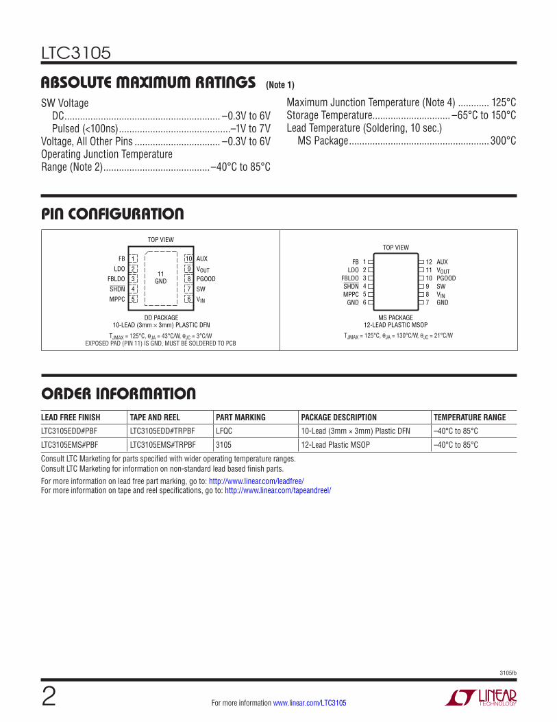
ABSOLUTE MAXIMUM RATINGSSW Voltage DC ............................................................ –0.3V to 6V Pulsed (<100ns) ...........................................–1V to 7VVoltage, All Other Pins ................................. –0.3V to 6VOperating Junction Temperature Range (Note 2) .........................................–40°C to 85°C
(Note 1)
TOP VIEW
11GND
DD PACKAGE10-LEAD (3mm × 3mm) PLASTIC DFN
10
9
6
7
8
4
5
3
2
1 AUX
VOUT
PGOOD
SW
VIN
FB
LDO
FBLDO
SHDN
MPPC
TJMAX = 125°C, θJA = 43°C/W, θJC = 3°C/W
EXPOSED PAD (PIN 11) IS GND, MUST BE SOLDERED TO PCB
123456
FBLDO
FBLDOSHDNMPPC
GND
121110987
AUXVOUTPGOODSWVINGND
TOP VIEW
MS PACKAGE12-LEAD PLASTIC MSOP
TJMAX = 125°C, θJA = 130°C/W, θJC = 21°C/W
PIN CONFIGURATION
ORDER INFORMATIONLEAD FREE FINISH TAPE AND REEL PART MARKING PACKAGE DESCRIPTION TEMPERATURE RANGE
LTC3105EDD#PBF LTC3105EDD#TRPBF LFQC 10-Lead (3mm × 3mm) Plastic DFN –40°C to 85°C
LTC3105EMS#PBF LTC3105EMS#TRPBF 3105 12-Lead Plastic MSOP –40°C to 85°C
Consult LTC Marketing for parts specified with wider operating temperature ranges. Consult LTC Marketing for information on non-standard lead based finish parts.For more information on lead free part marking, go to: http://www.linear.com/leadfree/ For more information on tape and reel specifications, go to: http://www.linear.com/tapeandreel/
Maximum Junction Temperature (Note 4) ............ 125°CStorage Temperature.............................. –65°C to 150°CLead Temperature (Soldering, 10 sec.) MS Package ...................................................... 300°C

LTC3105
33105fb
For more information www.linear.com/LTC3105
ELECTRICAL CHARACTERISTICS
Note 1: Stresses beyond those listed under Absolute Maximum Ratings may cause permanent damage to the device. Exposure to any Absolute Maximum Rating condition for extended periods may affect device reliability and lifetime.Note 2: The LTC3105 is tested under pulsed load conditions such that TJ ≈ TA. The LTC3105E is guaranteed to meet specifications from 0°C to 85°C junction temperature. Specifications over the –40°C to 85°C operating junction temperature range are assured by design, character-ization and correlation with statistical process controls. Note that the maximum ambient temperature consistent with these specifications is determined by specific operating conditions in conjunction with board layout, the rated package thermal impedance and other environmental factors.
The l denotes the specifications which apply over the full operating junction temperature range, otherwise specifications are at TA = 25°C (Note 2). VAUX = VOUT = 3.3V, VLDO = 2.2V, VIN = 0.6V, unless otherwise noted.PARAMETER CONDITIONS MIN TYP MAX UNITS
Step-Up Converter
Input Operating Voltage l 0.225 5 V
Input Start-Up Voltage (Note 5) TJ = 0°C to 85°C (Note 5)
l 0.25 0.4 0.36
V V
Output Voltage Adjust Range l 1.6 5.25 V
Feedback Voltage (FB Pin) l 0.984 1.004 1.024 V
VOUT IQ in Operation VFB = 1.10V 24 µA
VOUT IQ in Shutdown SHDN = 0V 10 µA
MPPC Pin Output Current VMPPC = 0.6V 9.72 10 10.28 µA
SHDN Input Logic High Voltage l 1.1 V
SHDN Input Logic Low Voltage l 0.3 V
N-Channel SW Pin Leakage Current VIN = VSW = 5V, VSHDN = 0V 1 10 µA
P-Channel SW Pin Leakage Current VIN = VSW = 0V, VOUT = VAUX = 5.25V 1 10 µA
N-Channel On-Resistance: SW to GND 0.5 Ω
P-Channel On-Resistance: SW to VOUT 0.5 Ω
Peak Current Limit VFB = 0.90V, VMPPC = 0.4V (Note 3) 0.4 0.5 A
Valley Current Limit VFB = 0.90V, VMPPC = 0.4V (Note 3) 0.275 0.35 A
PGOOD Threshold (% of Feedback Voltage) VOUT Falling 85 90 95 %
LDO Regulator
LDO Output Adjust Range External Feedback Network, VAUX > VLDO l 1.4 5 V
LDO Output Voltage VFBLDO = 0V l 2.148 2.2 2.236 V
Feedback Voltage (FBLDO Pin) External Feedback Network l 0.984 1.004 1.024 V
Load Regulation ILDO = 1mA to 6mA 0.40 %
Line Regulation VAUX = 2.5V to 5V 0.15 %
Dropout Voltage ILDO = 6mA, VOUT = VAUX = 2.2V 105 mV
LDO Current Limit VLDO 0.5V Below Regulation Voltage l 6 12 mA
LDO Reverse-Blocking Leakage Current VIN = VAUX = VOUT = 0V, VSHDN = 0V 1 µA
Note 3: Current measurements are performed when the LTC3105 is not switching. The current limit values measured in operation will be somewhat higher due to the propagation delay of the comparators.Note 4: This IC includes over temperature protection that is intended to protect the device during momentary overload conditions. Junction temperature will exceed 125°C when overtemperature protection is active. Continuous operation above the specified maximum operating junction temperature may impair device reliability. Note 5: The LTC3105 has been optimized for use with high impedance power sources such as photovoltaic cells and thermoelectric generators. The input start-up voltage is measured using an input voltage source with a series resistance of approximately 200mΩ and MPPC enabled. Use of the LTC3105 with lower resistance voltage sources or with MPPC disabled may result in a higher input start-up voltage.

LTC3105
43105fb
For more information www.linear.com/LTC3105
VOUT IQ vs Temperature During Shutdown
MPPC Current Variation vs Temperature
LDO Soft-Start Duration vs LDO Load
Minimum Input Start-Up Voltage vs Temperature
Shutdown Thresholds vs Input Voltage IC Enable Delay vs Input Voltage
TYPICAL PERFORMANCE CHARACTERISTICS TA = 25°C, VAUX = VOUT = 3.3V, VLDO = 2.2V, VIN = 0.6V, unless otherwise noted.
TEMPERATURE (°C)–45
INPU
T VO
LTAG
E (m
V)
280
–15 15 45
240
260
340
220
200
320
300
–30 0 75 9030 60
3105 G01
TEMPERATURE (°C)–45
CHAN
GE F
ROM
25°
C (%
)
0.5
–15 15 45
–0.5
2.0
0
2.5
–1.0
–1.5
1.5
1.0
–30 0 75 9030 60
3105 G05 LDO LOAD CURRENT (mA)1
0.95
SOFT
-STA
RT T
IME
(ms)
1.05
1.15
2 3 4 5
1.25
1.00
1.10
1.20
6
3105 G06
TEMPERATURE (°C)–45
I Q (µ
A)
12
22
–15 15 45
8
18
10
20
6
4
16
14
–30 0 75 9030 60
3105 G07
SHDN = 0V
SUPPLY VOLTAGE, VIN OR VAUX (V)1.25
0
THRE
SHOL
D VO
LTAG
E (m
V)
200
400
600
2.25 3.25 4.25
800
1000
100
300
500
700
900
5.25
3105 G02
IC DISABLE
IC ENABLE
DELA
Y TI
ME
(µs)
3105 G03SUPPLY VOLTAGE, VIN OR VAUX (V)
1.25 2.25 3.25 4.25 5.25
80
60
120
40
100
OUTPUT VOLTAGE (V)1.5
0
MAX
IMUM
INPU
T VO
LTAG
E (V
)
1.0
2.0
3.0
2.0 3.0 4.02.5 3.5 4.5 5.0
4.0
5.0
0.5
1.5
2.5
3.5
4.5
5.5
3105 G09
NONSYNCHRONOUSOPERATION
SYNCHRONOUSOPERATION
VIN for Synchronous Operation

LTC3105
53105fb
For more information www.linear.com/LTC3105
Exiting MPPC Control on Input Voltage Step
IPEAK and IVALLEY Current Limit Change vs Temperature
Input and Output Burst RippleEfficiency vs Output Current and Power Loss, VOUT = 3.3V
Efficiency vs Output Current and Power Loss, VOUT = 5V
No-Load Input Current vs Input Voltage
TYPICAL PERFORMANCE CHARACTERISTICS TA = 25°C, VAUX = VOUT = 3.3V, VLDO = 2.2V, VIN = 0.6V, unless otherwise noted.
INPUT VOLTAGE (V)0.2
0
INPU
T CU
RREN
T (µ
A)
200
400
600
0.4 0.6 0.8 1.0
800
100
300
500
700
1.2
3105 G16
VOUT = 3.3V
OUTPUT CURRENT (mA)
EFFI
CIEN
CY (%
)
POWER LOSS (m
W)
60
70
80
50
40
10
0
30
90
20
100
0.1
1000
10
1
3105 G14
VIN = 0.6VVIN = 0.8VVIN = 1V
EFFICIENCY
POWER LOSS
0.01 10.1 10 100
OUTPUT CURRENT (mA)0.01
EFFI
CIEN
CY (%
)
POWER LOSS (m
W)
60
70
80
50
40
10.1 10 100
30
100
90
20
100
0.1
1000
10
1
3105 G15
VIN = 3VVIN = 2VVIN = 1.5V
EFFICIENCY
POWER LOSS
TEMPERATURE (°C)–45
CHAN
GE F
ROM
25°
C (%
)
–0.5
–15 15 45
–1.5
–1.0
1.0
–2.0
–2.5
0.5
0
–30 0 75 9030 60
3105 G11
IVALLEY
IPEAK
15µs/DIV3105 G10
VIN VOLTAGE200mV/DIV
INDUCTORCURRENT100mA/DIV
MPPC VOLTAGE200mV/DIV
VMPPC = 400mV
INPUT VOLTAGE (V)0.25
40
EFFI
CIEN
CY (%
)
60
80
1.25 2.25 3.25 4.25
100
50
70
90
5.25
3105 G12
VOUT = 3VILOAD = 10mALDO = 2.2V
50µs/DIV3105 G13
OUTPUTVOLTAGE
50mV/DIV
INPUTVOLTAGE5mV/DIV
SW CURRENT200mA/DIV
VIN = 0.6VCIN = 470µF
VOUT = 3.3VIOUT = 15mACOUT = 10µF
Efficiency vs VIN

LTC3105
63105fb
For more information www.linear.com/LTC3105
PIN FUNCTIONSFB (Pin 1/Pin 1): Step-Up Converter Feedback Input. Connect the VOUT resistor divider tap to this input. The output voltage can be adjusted between 1.6V and 5.25V.
LDO (Pin 2/Pin 2): LDO Regulator Output. Connect a 4.7µF or larger capacitor between LDO and GND.
FBLDO (Pin 3/Pin 3): LDO Feedback Input. Connect the LDO resistive divider tab to this input. Alternatively, con-necting FBLDO directly to GND will configure the LDO output voltage to be internally set at 2.2V (nominal).
SHDN (Pin 4/Pin 4): Logic Controlled Shutdown Input. With SHDN open, the converter is enabled by an internal 2MΩ pull-up resistor. The SHDN pin should be driven with an open-drain or open-collector pull-down and floated until the converter has entered normal operation. Excessive loading on this pin may cause a failure to complete start-up.
SHDN = Low: IC Disabled
SHDN = High: IC Enabled
MPPC (Pin 5/Pin 5): Set Point Input for Maximum Power Point Control. Connect a resistor from MPPC to GND to program the activation point for the MPPC loop. To disable the MPPC circuit, connect MPPC directly to GND.
VIN (Pin 6/Pin 8): Input Supply. Connect a decoupling capacitor between this pin and GND. The PCB trace length from the VIN pin to the decoupling capacitor should be as short and wide as possible. When used with high imped-ance sources such as photovoltaic cells, this pin should have a 10µF or larger decoupling capacitor.
GND (Exposed Pad Pin 11/Pins 6, 7) : Small Signal and Power Ground for the IC. The GND connections should be soldered to the PCB ground using the lowest impedance path possible.
SW (Pin 7/Pin 9): Switch Pin. Connect an inductor between SW and VIN. PCB trace lengths should be as short as pos-sible to reduce EMI. While the converter is sleeping or is in shutdown, the internal antiringing switch connects the SW pin to the VIN pin in order to minimize EMI.
PGOOD (Pin 8/Pin 10): Power Good Indicator. This is an open-drain output. The pull-down is disabled when VOUT has achieved the voltage defined by the feedback divider on the FB pin. The pull-down is also disabled while the IC is in shutdown or start-up mode.
VOUT (Pin 9/Pin 11): Step-Up Converter Output. This is the drain connection of the main output internal synchronous rectifier. A 10µF or larger capacitor must be connected between this pin and GND. The PCB trace length from the VOUT pin to the output filter capacitor should be as short and wide as possible.
AUX (Pin 10/Pin 12): Auxiliary Voltage. Connect a 1µF capacitor between this pin and GND. This pin is used by the start-up circuitry to generate a voltage rail to power internal circuitry until the main output reaches regulation. AUX and VOUT are internally connected together once VOUT exceeds VAUX.
(DFN/MSOP)

LTC3105
73105fb
For more information www.linear.com/LTC3105
2MSHDN FBLDO
1.6V TO5.25V
VOUT
AUX
LDO
CIN10µF
RMPPC
L110µH
EXPOSED PAD
USER SHUTDOWN
SHUTDOWN
VALLEY CURRENT LIMIT
PEAK CURRENTLIMIT
VIN 6
4
7
11
9
+–
LOGICSLEEP
R3
R4
SHUTDOWN
CLDO4.7µF
1.004V
1.004V
SLEEPSHUTDOWN
VCC
VAUX
+–+–
+–
VIN
10µAMPPC
SW
5
LOW VOLTAGESTART-UP CURRENT
ADJUST
BURSTCONTROL
225mVTO 5V
+ –
3
PGOOD
FB1
10
2
R1
R2
COUT10µF
CAUX1µF
0.9V
FB8
3105 BD
SHORTCONTROL
WELLCONTROL
OR
VCC
SLEEP
VCCVAUX
VIN
gm
+–
BLOCK DIAGRAM (Pin Numbers for DFN Package Only)
LTC3105
83105fb
For more information www.linear.com/LTC3105
Introduction
The LTC3105 is a unique, high performance, synchronous boost converter that incorporates maximum power point control, 250mV start-up capability and an integrated LDO regulator. This part operates over a very wide range of input voltages from 225mV to 5V. Its Burst Mode architecture and low 24µA quiescent current optimize efficiency in low power applications.
An integrated maximum power point controller allows for operation directly from high impedance sources such as photovoltaic cells by preventing the input power source voltage from collapsing below the user programmable MPPC threshold. Peak current limits are automatically adjusted with proprietary techniques to maintain operation at levels that maximize power extraction from the source.
The 250mV start-up voltage and 225mV minimum operating voltage enable direct operation from a single photovoltaic cell and other very low voltage, high series impedance power sources such as TEGs and fuel cells.
Synchronous rectification provides high efficiency opera-tion while eliminating the need for external Schottky diodes. The LTC3105 provides output disconnect which prevents large inrush currents during start-up. This is particularly important for high internal resistance power sources like photovoltaic cells and thermoelectric generators which can become overloaded if inrush current is not limited during start-up of the power converter. In addition, output disconnect isolates VOUT from VIN while in shutdown.
VIN > VOUT Operation
The LTC3105 includes the ability to seamlessly maintain regulation if VIN becomes equal to or greater than VOUT. With VIN greater than or equal to VOUT, the synchro-nous rectifiers are disabled which may result in reduced efficiency.
Shutdown Control
The SHDN pin is an active low input that places the IC into low current shutdown mode. This pin incorporates an internal 2MΩ pull-up resistor which enables the converter if the SHDN pin is not controlled by an external circuit. The SHDN pin should be allowed to float while the part is in
OPERATIONstart-up mode. Once in normal operation, the SHDN pin may be controlled using an open-drain or open-collector pull-down. Other external loads on this pin should be avoided, as they may result in the part failing to reach regulation. In shutdown, the internal switch connecting AUX and VOUT is enabled.
When the SHDN pin is released, the LTC3105 is enabled and begins switching after a short delay. When either VIN or VAUX is above 1.4V, this delay will typically range be-tween 20µs and 100µs. Refer to the Typical Performance Characteristics section for more details.
Start-Up Mode Operation
The LTC3105 provides the capability to start with voltages as low as 250mV. During start-up the AUX output initially is charged with the synchronous rectifiers disabled. Once VAUX has reached approximately 1.4V, the converter leaves start-up mode and enters normal operation. Maximum power point control is not enabled during start-up, however, the currents are internally limited to sufficiently low levels to allow start-up from weak input sources.
While the converter is in start-up mode, the internal switch between AUX and VOUT remains disabled and the LDO is disabled. Refer to Figure 1 for an example of a typical start-up sequence.
The LTC3105 is optimized for use with high impedance power sources such as photovoltaic cells. For operation from very low impedance, low input voltage sources, it may be necessary to add several hundred milliohms of series input resistance to allow for proper low voltage start-up.
Normal Operation
When either VIN or VAUX is greater than 1.4V typical, the converter will enter normal operation.
The converter continues charging the AUX output until the LDO output enters regulation. Once the LDO output is in regulation, the converter begins charging the VOUT pin. VAUX is maintained at a level sufficient to ensure the LDO remains in regulation. If VAUX becomes higher than required to maintain LDO regulation, charge is transferred from the AUX output to the VOUT output. If VAUX falls too low, current is redirected to the AUX output instead of being used to charge the VOUT output. Once VOUT rises

LTC3105
93105fb
For more information www.linear.com/LTC3105
3105 F01
OUTP
UT V
OLTA
GEIN
DUCT
OR C
URRE
NT
TIME
TIME
NORMAL OPERATION
LDO INREGULATION
1.4V
VOUT SYNCHRONOUSRECTIFIER ENABLED
VAUX VOUT
VOUT INREGULATION
VOUT = VAUX
START-UP MODE
VLDO
above VAUX, an internal switch is enabled to connect the two outputs together.
If VIN is greater than the voltage on the driven output (VOUT or VAUX), or the driven output is less than 1.2V (typical), the synchronous rectifiers are disabled. With the synchro-nous rectifiers disabled, the converter operates in critical conduction mode. In this mode, the N-channel MOSFET between SW and GND is enabled and remains on until the inductor current reaches the peak current limit. It is then disabled and the inductor current discharges completely before the cycle is repeated.
When the output voltage is greater than the input voltage and greater than 1.2V, the synchronous rectifier is enabled. In this mode, the N-channel MOSFET between SW and GND is enabled until the inductor current reaches the peak current limit. Once current limit is reached, the N-channel MOSFET turns off and the P-channel MOSFET between SW and the driven output is enabled. This switch remains on until the inductor current drops below the valley current limit and the cycle is repeated.
Figure 1. Typical Converter Start-Up Sequence
When VOUT reaches the regulation point, the N- and P-channel MOSFETs connected to the SW pin are disabled and the converter enters sleep.
Auxiliary LDO
The integrated LDO provides a regulated 6mA rail to power microcontrollers and external sensors. When the input voltage is above the minimum of 225mV, the LDO is powered from the AUX output allowing the LDO to attain regulation while the main output is still charging. The LDO has a 12mA current limit and an internal 1ms soft-start to eliminate inrush currents. The LDO output voltage is set by the FBLDO pin. If a resistor divider is connected to this pin, the ratio of the resistors determines the LDO output voltage. If the FBLDO pin is connected directly to GND, the LDO will use a 2MΩ internal divider network to program a 2.2V nominal output voltage. The LDO should be programmed for an output voltage less than the pro-grammed VOUT.
OPERATION

LTC3105
103105fb
For more information www.linear.com/LTC3105
When the converter is placed in shutdown mode, the LDO is forced into reverse-blocking mode with reverse current limited to under 1µA. After the shutdown event has ended, the LDO remains in reverse-blocking mode until VAUX has risen above the LDO voltage.
MPPC Operation
The maximum power point control circuit allows the user to set the optimal input voltage operating point for a given power source. The MPPC circuit dynamically regulates the average inductor current to prevent the input voltage from dropping below the MPPC threshold. When VIN is greater than the MPPC voltage, the inductor current is increased until VIN is pulled down to the MPPC set point. If VIN is less than the MPPC voltage, the inductor current is reduced until VIN rises to the MPPC set point.
Automatic Power Adjust
The LTC3105 incorporates a feature that maximizes ef-ficiency at light load while providing increased power
capability at heavy load by adjusting the peak and valley of the inductor current as a function of load. Lowering the peak inductor current to 100mA at light load optimizes efficiency by reducing conduction losses. As the load increases, the peak inductor current is automatically in-creased to a maximum of 500mA. At intermediate loads, the peak inductor current can vary between 100mA to 500mA. This function is overridden by the MPPC function and will only be observed when the power source can deliver more power than the load requires.
PGOOD Operation
The power good output is used to indicate that VOUT is in regulation. PGOOD is an open-drain output, and is disabled in shutdown. PGOOD will indicate that power is good at the beginning of the first sleep event after the output voltage has risen above 90% of its regulation value. PGOOD remains asserted until VOUT drops below 90% of its regulation value at which point PGOOD will pull low.
OPERATION
Component Selection
Low DCR power inductors with values between 4.7µH and 30µH are suitable for use with the LTC3105. For most applications, a 10µH inductor is recommended. In applications where the input voltage is very low, a larger value inductor can provide higher efficiency and a lower start-up voltage. In applications where the input voltage is relatively high (VIN > 0.8V), smaller inductors may be used to provide a smaller overall footprint. In all cases, the inductor must have low DCR and sufficient saturation current rating. If the DC resistance of the inductor is too high, efficiency will be reduced and the minimum operating voltage will increase.
Input capacitor selection is highly important in low voltage, high source resistance systems. For general applications, a 10µF ceramic capacitor is recommended between VIN and GND. For high impedance sources, the input capacitor
APPLICATIONS INFORMATIONshould be large enough to allow the converter to complete start-up mode using the energy stored in the input ca-pacitor. When using bulk input capacitors that have high ESR, a small valued parallel ceramic capacitor should be placed between VIN and GND as close to the converter pins as possible.
A 1µF ceramic capacitor should be connected between AUX and GND. Larger capacitors should be avoided to minimize start-up time. A low ESR output capacitor should be connected between VOUT and GND. The main output capacitor should be 10µF or larger. The main output can also be used to charge energy storage devices including tantalum capacitors, supercapacitors and batteries. When using output bulk storage devices with high ESR, a small valued ceramic capacitor should be placed in parallel and located as close to the converter pins as possible.

LTC3105
113105fb
For more information www.linear.com/LTC3105
APPLICATIONS INFORMATIONStep-Up Converter Feedback Configuration
A resistor divider connected between the VOUT and FB pins programs the step-up converter output voltage, as shown in Figure 2. An optional 22pF feedforward capacitor, CFF1, can be used to reduce output ripple and improve load transient response. The equation for VOUT is:
VOUT = 1.004V •
R1R2
+ 1
LDO Regulator Feedback Configuration
Two methods can be used to program the LDO output voltage, as shown in Figure 3. A resistor divider connected between the LDO and FBLDO pins can be used to program the LDO output voltage. The equation for the LDO output voltage is:
VLDO = 1.004V •
R3R4
+ 1
Alternatively, the FBLDO pin can be connected directly to GND. In this configuration, the LDO is internally set to a nominal 2.2V output.
Figure 2. FB Configuration
3105 F02
LTC3105CFF1 R1
R2
FB
VOUT
Figure 3. FBLDO Configuration
3105 F03
LDO
LTC3105R3
2.2V
R4
LDO
FBLDO FBLDO
LTC3105
MPPC Threshold Configuration
The MPPC circuit controls the inductor current to main-tain VIN at the voltage on the MPPC pin. The MPPC pin voltage is set by connecting a resistor between the MPPC pin and GND, as shown in Figure 4. The MPPC voltage is determined by the equation:
VMPPC = 10µA • RMPPC
In photovoltaic cell applications, a diode can be used to set the MPPC threshold so that it tracks the cell voltage over temperature, as shown in Figure 5. The diode should be thermally coupled to the photovoltaic cell to ensure proper tracking. A resistor placed in series with the diode can be used to adjust the DC set point to better match the maximum power point of a particular source if the selected diode forward voltage is too low. If the diode is located far from the converter inputs, a capacitor may be required to filter noise that may couple onto the MPPC pin, as shown in Figure 5. This method can be extended to stacked cell sources through use of multiple series connected diodes.
Figure 4. MPPC Configuration
Figure 5. MPPC Configuration with Temperature Adjustment
3105 F04
MPPC
LTC3105RMPPC
10µA
3105 F05
MPPC
LTC3105
C610nFVFWD
RMPPC
10µA
+
–

LTC3105
123105fb
For more information www.linear.com/LTC3105
TEMPERATURE (°C)–45
MPP
C VO
LTAG
E (V
)
0.4
–15 15 45
0.2
0.3
0.7
0.1
0
0.6
0.5
–30 0 75 9030 60
3105 TA02a
25µs/DIV
3105 TA02b
INPUT CURRENT25mA/DIV
OUTPUT CURRENT5mA/DIV
INPUT VOLTAGE50mV/DIV
VOUT = 2.8VVMPPC = 0.4VVFB = 0.94V
0.38V
10mA
0.7mA
APPLICATIONS INFORMATIONIndustrial Current Loops
The low 250mV start-up and low voltage operation of the LTC3105 allow it to be supplied by power from a diode placed in an industrial sensor current loop, as shown in Figure 6. In this application, a large input capacitor is required due to the very low available supply current (less than 4mA). The loop diode should be selected for a minimum forward drop of 300mV. The MPPC pin voltage should be set for a value approximately 50mV below the minimum diode forward voltage.
Figure 6. Current Loop Power Tap
3105 F06
GND
MPPC
VIN
LTC3105CINVFWD
RMPPC
4mA TO 20mACURRENT LOOP +
–
3.3V from a Single-Cell Photovoltaic Source with Temperature Tracking
VMPPC vs Temperature MPPC Response to Input Source Current Step
3105 TA02
COUT10µF
R12.26M
VOUT3.3V
R21M
FB
PGOOD
LDO
FBLDO
MPPC
SHDN
AUX
SW
CLDO4.7µF
2.2VRMPPC9.09k
CAUX1µF
* MRA4003T3** COILCRAFT MSS5131-103MX
LTC3105
CMPPC10nF GND
CIN10µF
L1**10µH
+
–
ONOFF
VIN
VOUT
D1*
THERMALLYCOUPLED
TYPICAL APPLICATIONS

LTC3105
133105fb
For more information www.linear.com/LTC3105
TYPICAL APPLICATIONS3.3V from Multiple Stacked-Cell Photovoltaic with Source Temperature Tracking
Thermoelectric Generator to 2.4V Super Capacitor Charger
3105 TA03
COUT10µF
R11.37M
VOUT3.3V
R2604k
FB
PGOOD
LDO
FBLDO
MPPC
SHDN
AUX
SW
CLDO4.7µF
2.2V
CAUX1µF
RMPPC4.99k
CIN10µF
* MRA4003T3** PANASONIC ELL-VEG6R8N
L1**6.8µH
LTC3105
CMPPC10nF
GND
+
–+
–
ONOFF
VIN
VOUT
D1*
D2*
THERMALLYCOUPLED
3105 TA04
CBULK1F2.5V
R11.10M
VOUT2.4V
R2787k
FB
PGOOD
LDO
FBLDO
MPPC
VIN
SHDN
AUX
SW
VOUT
CLDO4.7µF
2.2V
CFF22pF
RMPPC30.1k
* MICROPELT MPG-D751** COILCRAFT MSS5131-103MX
TEG*
∆T ≥ 10°C
CAUX1µF
CIN100µF
L1**10µH
LTC3105
GND
COUT1µF
ONOFF+
+

LTC3105
143105fb
For more information www.linear.com/LTC3105
2ms/DIV3105 TA05a
VIN VOLTAGE50mV/DIV
LOAD CURRENT2mA/DIV
VOUT VOLTAGE250mV/DIV
50ms/DIV 3105 TA05b
VIN VOLTAGE200mV/DIV
LDO VOLTAGE500mV/DIV
VOUT VOLTAGE500mV/DIV
100mV
0V
TYPICAL APPLICATIONSIndustrial Sensor 4mA to 20mA Current Loop Power Tap
Transient Response to Load Pulse with 4mA Loop Current Start-Up VIN, VOUT, VLDO
3105 TA05
R12M
VOUT, 3V
R21M
FB
ENPGOOD
LDO
FBLDO
MPPC
SHDN
AUX
SW
µP
CAUX1µF
RMPPC28k
280mV2.2V
CIN470µF
4mA TO 20mACURRENT LOOP
D1*
L1**10µH
LTC3105
GND
10µF
VFWD = 330mV
RPG499k
* MBRS190T3** COILCRAFT MSS5131-103MX
+
–ONOFF
VIN
VDD
VOUT
CLDO4.7µF
Single-Cell Photovoltaic NiMH Trickle Charger
3105 TA06
NiMH× 2
R11.02M
VOUT3.2V
R2470k
FB
PGOOD
LDO
FBLDO
MPPC
SHDN
AUX
SW
CLDO4.7µF
1.8V
RMPPC40.2k
CAUX1µF
CIN10µF
L1, 10µH
LTC3105
GND
COUT10µF
R31M
R41.27M
+
+
+
–
ONOFF
VIN
VOUT

LTC3105
153105fb
For more information www.linear.com/LTC3105
PACKAGE DESCRIPTION
3.00 ±0.10(4 SIDES)
NOTE:1. DRAWING TO BE MADE A JEDEC PACKAGE OUTLINE M0-229 VARIATION OF (WEED-2). CHECK THE LTC WEBSITE DATA SHEET FOR CURRENT STATUS OF VARIATION ASSIGNMENT2. DRAWING NOT TO SCALE3. ALL DIMENSIONS ARE IN MILLIMETERS4. DIMENSIONS OF EXPOSED PAD ON BOTTOM OF PACKAGE DO NOT INCLUDE MOLD FLASH. MOLD FLASH, IF PRESENT, SHALL NOT EXCEED 0.15mm ON ANY SIDE5. EXPOSED PAD SHALL BE SOLDER PLATED6. SHADED AREA IS ONLY A REFERENCE FOR PIN 1 LOCATION ON THE TOP AND BOTTOM OF PACKAGE
0.40 ±0.10
BOTTOM VIEW—EXPOSED PAD
1.65 ±0.10(2 SIDES)
0.75 ±0.05
R = 0.125TYP
2.38 ±0.10(2 SIDES)
15
106
PIN 1TOP MARK
(SEE NOTE 6)
0.200 REF
0.00 – 0.05
(DD) DFN REV C 0310
0.25 ±0.05
2.38 ±0.05(2 SIDES)
RECOMMENDED SOLDER PAD PITCH AND DIMENSIONS
1.65 ±0.05(2 SIDES)2.15 ±0.05
0.50BSC
0.70 ±0.05
3.55 ±0.05
PACKAGEOUTLINE
0.25 ±0.050.50 BSC
DD Package10-Lead Plastic DFN (3mm × 3mm)
(Reference LTC DWG # 05-08-1699 Rev C)
PIN 1 NOTCHR = 0.20 OR0.35 × 45°CHAMFER
Please refer to http://www.linear.com/product/LTC3105#packaging for the most recent package drawings.

LTC3105
163105fb
For more information www.linear.com/LTC3105
PACKAGE DESCRIPTION
MSOP (MS12) 0213 REV A
0.53 ±0.152(.021 ±.006)
SEATINGPLANE
0.18(.007)
1.10(.043)MAX
0.22 – 0.38(.009 – .015)
TYP
0.86(.034)REF
0.650(.0256)
BSC
12 11 10 9 8 7
NOTE:1. DIMENSIONS IN MILLIMETER/(INCH)2. DRAWING NOT TO SCALE3. DIMENSION DOES NOT INCLUDE MOLD FLASH, PROTRUSIONS OR GATE BURRS. MOLD FLASH, PROTRUSIONS OR GATE BURRS SHALL NOT EXCEED 0.152mm (.006") PER SIDE4. DIMENSION DOES NOT INCLUDE INTERLEAD FLASH OR PROTRUSIONS. INTERLEAD FLASH OR PROTRUSIONS SHALL NOT EXCEED 0.152mm (.006") PER SIDE5. LEAD COPLANARITY (BOTTOM OF LEADS AFTER FORMING) SHALL BE 0.102mm (.004") MAX
0.254(.010) 0° – 6° TYP
DETAIL “A”
DETAIL “A”
GAUGE PLANE
5.10(.201)MIN
3.20 – 3.45(.126 – .136)
0.889 ±0.127(.035 ±.005)
RECOMMENDED SOLDER PAD LAYOUT
0.42 ±0.038(.0165 ±.0015)
TYP
0.65(.0256)
BSC
4.039 ±0.102(.159 ±.004)
(NOTE 3)
0.1016 ±0.0508(.004 ±.002)
1 2 3 4 5 6
3.00 ±0.102(.118 ±.004)
(NOTE 4)
0.406 ±0.076(.016 ±.003)
REF
4.90 ±0.152(.193 ±.006)
MS Package12-Lead Plastic MSOP
(Reference LTC DWG # 05-08-1668 Rev A)
Please refer to http://www.linear.com/product/LTC3105#packaging for the most recent package drawings.

LTC3105
173105fb
For more information www.linear.com/LTC3105
Information furnished by Linear Technology Corporation is believed to be accurate and reliable. However, no responsibility is assumed for its use. Linear Technology Corporation makes no representa-tion that the interconnection of its circuits as described herein will not infringe on existing patent rights.
REVISION HISTORYREV DATE DESCRIPTION PAGE NUMBER
A 01/11 Added (Note 5) notation to Input Start-Up Voltage conditions.Added Note 5.Updated Start-Up Mode Operation section.
338
B 11/15 VOUT range changed.Changed G09 curve.Changed feedback description.Changed VOUT range.
3467

LTC3105
183105fb
For more information www.linear.com/LTC3105 LINEAR TECHNOLOGY CORPORATION 2010
LT 1115 REV B • PRINTED IN USALinear Technology Corporation1630 McCarthy Blvd., Milpitas, CA 95035-7417(408) 432-1900 ● FAX: (408) 434-0507 ● www.linear.com/LTC3105
RELATED PARTS
TYPICAL APPLICATION
PART NUMBER DESCRIPTION COMMENTS
LTC3106 300mA Low Voltage Buck-Boost Converter with PowerPath™ and 1.6μA Quiescent Current
300mV ≤ VIN ≤ 5.1V; Selectable Output Voltages Primary or Rechargeable Backup Batteries, MPPC, 3mm × 4mm QFN-20, TSSOP-20E Packages, Solar and TEG
LTC3330 Dual Input Nanopower Buck-Boost DC/DC with Energy Harvesting Battery Life Extender, Input Prioritizer and Up to 50mA of IOUT
3V ≤ VIN ≤ 19V for EH; 1.8V ≤ VIN ≤ 5V for Battery Full-Wave Bridge Rectifier, Super Cap Balancer 5mm × 5mm QFN-32, Solar and Vibration
LTC3331 Dual Input Nanopower Buck-Boost DC/DC with Energy Harvesting 10mA Shunt Battery Charger Input Prioritizer and Up to 50mA of IOUT
3V ≤ VIN ≤ 19V for EH; 1.8V ≤ VIN ≤ 4.2V for Battery Full-Wave Bridge Rectifier, Super Cap Balancer Programmable Float Voltages, 5mm × 5mm QFN-32, Solar and Vibration
LTC3109 Auto-Polarity, Ultralow Voltage Step-Up Converter and Power Manager
±0.03V ≤ VIN ≤ ±0.50V, Selectable VOUT of 2.35V, 3.3V, 4.1V or 5V Uses Compact Step-Up Transformers, IQ = 7μA; 4mm × 4mm QFN-20 SSOP-20 Packages, TEG and Thermopiles
LTC3108/LTC3108-1
Ultralow Voltage Step-Up Converter and Power Manager
0.03V ≤ VIN ≤ 0.50V, Selectable VOUT of 2.5V, 3V, 3.7V or 4.5V Uses Compact Step-Up Transformers, IQ = 7μA; 3mm × 4mm DFN-12 SSOP-16 Packages, TEG and Thermopiles
LTC4070 Li-Ion/Polymer Shunt Battery Charger System 450nA IQ; 1% Float Voltage Accuracy; 50mA Shunt Current 4.0V/4.1V/4.2V, DFN-8 and MSOP-8E Packages
LTC4071 Li-Ion/Polymer Shunt Battery Charger System with Low Battery Disconnect
550nA IQ; 1% Float Voltage Accuracy; <10nA Low Battery Disconnect; 4.0V/4.1V/4.2V; 8-Lead 2mm × 3mm DFN and MSOP Packages
LTC3588-1/LTC3588-2
Piezoelectric Energy Harvesting Power Supply < 1µA IQ in Regulation; 2.7V to 20V Input Range; Integrated Bridge Rectifier. MSOP-10E and 3mm × 3mm DFN-10 Packages
Single-Cell Powered Remote Wireless Sensor
3105 TA07
R12.32M
VOUT3.3V
R21.02M
FB
PGOOD
LDO
A/D
I/O
XMTR
SENSORµC
FBLDO
MPPC
EN
SHDN
AUX
SW
CLDO4.7µF
2.2V
RMPPC40.2k
RPG499k
CAUX1µF
CIN10µF
L1*10µH
LTC3105
GND GND
COUT100µF
VDD GPIO
* COILCRAFT MSS5131-103MX
2N7000
ONOFF
VIN
VOUT
+
–