lt journal - march 2005...after evaluating various lead-free alternatives, linear technology...
TRANSCRIPT

LINEAR TECHNOLOGYLINEAR TECHNOLOGYLINEAR TECHNOLOGYMARCH 2005 VOLUME XV NUMBER 1
a closed loop battery-charge system, and upgrade components as needed. All of the safety features are taken into account within the battery. This minimizes NRE costs and makes for robust systems, especially important to high reliability battery-backup ap-plications. There is no need to become a battery expert to take advantage of the features of the SBS.
The first part of this article offers an overview of the SBS; the second part describes two of Linear Technology’s Smart Battery Chargers.
, LTC, LT, Burst Mode, OPTI-LOOP, Over-The-Top and PolyPhase are registered trademarks of Linear Technology Cor-poration. Adaptive Power, C-Load, DirectSense, FilterCAD, Hot Swap, LinearView, Micropower SwitcherCAD, Multimode Dimming, No Latency ΔΣ, No Latency Delta-Sigma, No RSENSE, Operational Filter, PanelProtect, PowerPath, PowerSOT, SmartStart, SoftSpan, Stage Shedding, SwitcherCAD, ThinSOT, UltraFast and VLDO are trademarks of Linear Technology Corporation. Other product names may be trademarks of the companies that manufacture the products.
Smart Batteries: Not Just for Notebooks Anymore
by Mark GurriesIntroductionWith the backing of Intel and Micro-soft, Smart Batteries have become the dominant battery pack solution for products that require an accurate gas gauge to predict battery life. The Smart Battery System (SBS) has simplified the design of standalone battery sys-tems so much that it is showing up in applications outside its usual realm of notebook computers. For instance, the SBS is gaining popularity in backup power systems for mission critical high reliability applications.
The attraction of the SBS is that its modular nature makes easy to design continued on page 3
IN THIS ISSUE…
COVER ARTICLESmart Batteries: Not Just for Notebooks Anymore ....................... 1Mark Gurries
Issue Highlights ............................ 2LTC in the News… .......................... 2
DESIGN FEATURESDual Monolithic Ideal Diodes Provide a Single-Chip Power Management Solution .................... 7Andy Bishop
Simplify PoE Implementation with Complete PD Interface and Integrated Switching Regulator .................................................... 11Kirk Su
High Accuracy Clock up to 170MHz in a SOT-23 ........... 14Albert Huntington
Simple, Precise Instrumentation Amplifier Features Digitally Programmable Gains from 1 to 4096 .................................................... 16Michael Kultgen
Flexible Power Supply Sequencing and Monitoring ......... 20Jeff Heath and Akin Kestelli
High Voltage Step-Down Synchronous Controller Offers Single-Supply Operation, Current Mode Control, and 100µA Burst Mode® Operation .......................... 25Jay Celani
DESIGN IDEAS ............................................... 29–36(complete list on page 29)
New Device Cameos ...................... 37Design Tools ................................ 39Sales Offices ................................ 40
PROTECTIONCIRCUIT
DISCHARGE CHARGE
GAS GAUGE
SAFETYSIGNAL
SMARTBATTERYCHARGER
UNRE
GULA
TED
POW
ER(W
ALL
ADAP
TER)
CLK
DATA
CLK
DATA
CLK
DATA
BATTERYCELLS
CURRENTSENSE
SMBUS
SMART BATTERY
Figure 1. Simplified schematic of a Smart Battery and Smart Battery Charger. Smart Batteries have an integrated gas gauge, which communicates the condition of the battery, and requests charge (voltage and current) over the SMBus. Charge requests are satisfied by the Smart Battery Charger, which applies the requested voltage and current to the battery terminals. The beauty of the system is that the charger does not need to know the chemistry of the battery. It is up to the gas gauge to maintain the charge algorithms. The modular nature of the SBS allows for any Smart Battery Charger to charge any Smart Battery.

2 Linear Technology Magazine • March 20052
EDITOR’S PAGE
power point-of-load requirements of distributed power systems. (Page 25)
Design Ideas and CameosThe Design Ideas start on page 29, including a low harmonic distortion, amplitude stable sine wave generator using the LT1968 RMS-to-DC con-verter. Five New Device Cameos appear on page 37.
solution for multivoltage-rail sys-tems, such as telecommunications equipment, memory modules, optical systems, networking equipment, serv-ers, and base stations. (Page 20)
High Voltage DC/DC Conversion The LT®3800 is a feature-packed high voltage synchronous step-down controller that helps meet the high-
Issue Highlights
Linear Technology in the News…Linear Technology Offers All Products in Lead-Free Versions as Part of Broader Commitment to Protecting the Environment All of Linear Technology’s products are now available in lead-free ver-sions as an ordering option. This is part of the company’s commitment to meeting the European Community’s Reduction of Hazardous Substances (RoHS) guidelines, and represents the latest step in Linear Technology’s ongoing commitment to excellence and leadership in protecting the en-vironment.
After evaluating various lead-free alternatives, Linear Technology se-lected Matte Tin as the optimal plating for lead-free products. The company believes that this provides the best drop-in replacement since it has the lowest reflow temperature of the lead-free alternatives, has excellent sol-derability performance, and provides excellent quality and reliability. In order to ensure a smooth transition for customers, Linear Technology will continue to offer solder plated products as well, with unique part numbers for both the lead-free and solder plated versions.
In addition to offering lead-free plating, Linear Technology will also provide by mid-2005 an improved plastic mold compound that eliminates antimony trioxide and elemental bromine for a more environmentally friendly packaging alternative. The company’s goal is to replace these flame retardants with environmentally friendly alternatives that meet flammability standards, while improving the product reliability.
In early 2002, Linear Technology was certified to ISO 14001 compliance by implementing an environmental management system. The company is dedicated to making an ongoing contribution to environmental excellence in all of its operations.
Electronic Products Magazine Awards Linear Technology “Product of the Year” for Compact Photoflash Capacitor ChargerFrom the thousands of products introduced in 2004, the editors of Electronic Products have chosen what they feel are among the most outstanding—based on significant advances in technology or its application, a decided innovation in design, or a substantial gain in price-performance.
The LT3468 photoflash capacitor charger is one of these products (see Electronic Products, Jan. 2004, p. 84 and Linear Technology Magazine, Dec. 2003, p. 1). It enables the use of a Xenon flash lamp in a 3-Mpixel camera phone—providing excellent photographic performance in a small form factor and at a reasonable cost.
With the backing of Intel and Microsoft, Smart Batteries have become the dominant battery
pack solution for products that require an accurate gas gauge to predict bat-tery life. The Smart Battery System (SBS) has simplified the design of standalone battery systems so much that it is showing up in applications outside its usual realm of notebook computers.
Our cover article shows how Linear Technology’s Smart Battery Charger circuits simplify the design of high per-formance Smart Battery Systems.
Featured DevicesBelow is a summary of the other de-vices featured in this issue.
Complete PowerPath™ Management Squeezed into 9mm2
The LTC®4413 dual monolithic ideal diode makes it possible to build an entire power management solution in a 3mm × 3mm footprint. (Page 7)
Power over Ethernet Simplified The LTC4267 reduces the complexity and size of a PD by combining an IEEE 802.3af-compliant PD interface with a current mode switching regulator in a space-saving, low-profile 16-pin SSOP or DFN package. (Page 11)
Tougher than a Crystal Oscillator: An All Silicon ClockThe LTC6905 is an all silicon clock that avoids the pitfalls of sensitive and power hungry crystal oscillators. (Page 14)
Wide Range, Digitally Programmable Voltage GainThe LTC6915 is the simplest, most precise way to obtain digitally pro-grammable voltage gain. (Page 16)
Combo Power Supply Sequencer and SupervisorThe LTC2924 is a complete power supply sequencer and supervisor

Linear Technology Magazine • March 2005 3
DESIGN FEATURES
About the Smart Battery SystemFigure 1 shows a simplified block diagram of a Smart Battery. The biggest benefit of the Smart Battery System is the highly accurate gas gauge integrated into the battery pack. The gas gauge, as the name implies, indicates how much energy is left in the battery.
An integrated gas gauge can moni-tor the battery even when the battery is on the shelf, and the gas gauge is calibrated to a single battery, so ac-curacy is assured. A host-based gas gauge can’t match this. Gas gauge measurement techniques have evolved to the point that the latest gas gauges are self-calibrating—error rates are at 1% over the lifetime of the battery. Because the gas gauge knows the battery better than any other circuit can, it is responsible for charge and discharge management.
Smart Battery ChargersIn an SBS Li-ion battery pack, there are built-in MOSFETS that can block charge or discharge current (see Fig-ure 1). The SBS gas gauge can easily prevent over-discharge by turning off the discharge MOSFET when the bat-tery voltage reaches a certain point; but when it comes to charging the bat-
tery, the gas gauge must work with an external charger. Smart Batteries are designed to work with Smart Battery Chargers. A Smart Battery Charger has advantages over a fixed standalone charger, such as: True Plug and Play operation,
independent of battery chemistry and cell-configuration. Any Smart Battery Pack will work with any Smart Battery Charger. Batteries with different chemistries, cell-configurations, and even differ-ent charge algorithms can be swapped with no modification to the charger circuit.
Built in safety features. The bat-tery, because of its gas gauge, takes care of itself.
A reliable battery detection sys-tem.
Automatic charge management without the need of a host pro-cessor.
Any Smart Battery and Smart Charger form a closed loop charge system that requires no
host processor intervention. A host is welcome to gather gas gauge information if required.To understand how all this is pos-
sible, let’s see how the Smart Battery system actually works.
How SMBus is used for a Closed Loop Charge ProcessThe Smart Battery System utilizes the System Management Bus or SMBus standard, which is a based on, and a subset of, the very popular and now recently made public domain two wire I2C serial bus standard. In practice SMBus devices easily coexist with I2C devices on the same bus.
The Smart Battery Standard defines fixed addresses for the battery and charger, and it defines some com-mands that allow the gas gauge to communicate to the Smart Battery Charger over the SMBus. This forms a closed loop system where the gas gauge determines the charge state of the bat-tery, and evaluates other conditions (such as battery temperature) to see
Smart Batteries, continued from page 1
VDD
DCDIV
CHGEN
ACP
SMBALERT
SCL
SDA
THB
THA
ILIM
VLIM
IDC
DCIN
INFET
CLP
CLN
TGATE
BGATE
PGND
CSP
BAT
VSET
ITH
GND
17
11
6
10
7
9
8
15
16
13
14
20
5
4
24
23
1
3
2
21
22
18
19
12
LTC4100
3VTO 5.5V
0.12µF
0.1µF
0.082µF 0.1µF
0.01µF
0.0015µF6.04k10k
54.9k
100Ω
0.033Ω
20µF
20µF
0.1µF
10µH
0.025Ω
SMBCLK
4.99k
SMBDAT
SMBCLK
SMBDAT
DCIN
CHGEN
SMBALERT#
ACP SMART BATTERY
1.13k
1.21k13.7k
SafetySignal
Figure 2. The LTC4100 in a feature-rich, simple and compact 4A Smart Battery charger
More Information about Smart Batteries… SBS gas gauge ...................www.sbs-forum.org/specs/sbdat110.pdf Smart Batter Charger ........www.sbs-forum.org/specs/sbc110.pdf Smart Battery System Manager
(SBSM) ..............................www.sbs-forum.org/specs/sbsm100b.pdf SMBus ..............................www.smbus.org/specs

4 Linear Technology Magazine • March 2005
DESIGN FEATURES
allows the charger to make its own determination, independent of the gas gauge.
Alarms Warn of Impending ProblemsAn active safety feature called alarms is available to the Smart Battery. Alarms cover temperature, overcharge and over-discharge fault conditions, and are sent when the battery is close to taking direct action to stop the condi-tion of concern. The gas gauge can send alarms to both the host and the Smart Battery Charger via the SMBus.
Over-Discharge Recovery Over-discharge presents a special challenge that is fully addressed by the Smart Battery System. What happens if the battery does not have enough charge to support SMBus communica-tions? One cannot attempt to detect the battery via its terminals, since the gas gauge will have already turned off the discharge MOSFET to protect the battery cells. A Smart Battery Charger, though, can use the safety signal to check for the battery pack, regardless of its state of charge.
A Smart Battery Charger, upon detection of a new battery, applies a constant current charge up to 100mA to the battery terminals. This low cur-rent quickly charges the cells enough
if a safe charge can be performed. The gas gauge requests a charge current and voltage from the Smart Charger via the SMBus. Because the gas gauge is in charge, the charger is not burdened with algorithms involving the battery cell configuration or chemistry.
When the gas gauge requests charge, the Smart Charger evaluates the requested charge parameters and does the best job it can to comply with them while at the same time independently evaluating various safety conditions. In order for charge process to happen, both the battery and the charger must agree it is safe to proceed. This keeps the loop simple and safe.
Flexible CommunicationsAlthough the SMBus standard only allows a single battery and a single charger to exist on a bus, multiple bus masters can coexist on the same bus. This allows the “Smarts” of the Smart Battery System to be distributed or augmented.
If you read Smart Battery Specifi-cations, you might come across the terms called levels such as level 2 and level 3. This has nothing to do with sophistication or revision levels. It simply is a way of defining who is primarily responsible for the com-munication of charge request between the battery and the charger. A level 2 system means the Smart Battery is an SMBus bus master and transmits its charge commands to the charger directly. This is the simplest loop. A level 3 system means any device other than the Smart Battery itself, such as a host, is responsible for sending the commands to the charger. The latter configuration allows for other devices to take more control of the process to implement other unique features beyond those available by default with a level 2 system. Linear technology takes advantage of that capability in the LTC1760 smart charger by build-ing the bus master into the charger. This allows for parallel charge and discharge of dual batteries, which has numerous advantages, explained in the “LTC1760 Dual Smart Battery Charger” section, below.
Safety and Reliability in the SMBusThe SMBus standard incorporates fail-safe mechanisms for SMBus crashes or hangs that allow bus recovery. The charger has watchdog timers that monitor the frequency of charge request commands, and can detect a loss of communication or closed loop operation so that it can pause the charge process and prevent accidental overcharge. For Li-ion batteries this is critically important.
Battery Detection via the Safety Signal Reliable battery detection and addi-tional safety is achieved by use of the Safety Signal, formerly known as the thermistor signal. The Safety Signal is produced by applying a voltage to a resistor, or thermistor in the Smart Battery via the dedicated SS pin (see Figure 1). A Smart Charger can mea-sure the value of the resistance of the SS pin to ground, and from the resulting value, know if the battery is physically present, and if an NTC thermistor is present, determine if the temperature range is acceptable to allow charge.
The thermistor on the Safety Signal is not the same thermistor the gas gauge uses to evaluate temperature. It is a redundant system check that
SWITCH MATRIXCIRCUITRY FOR
POWERPATH CONTROL AND SMBUS
CHARGER4A MAX
LEVEL 3POWER MANAGER
LTC1760
DC/DCCONVERTER BATTERY 1
BATTERY 2SYSTEM
HOST
SMBUS 1 & SAFETY SIGNAL
SYSTEM POWER
SMBUS
LOGIC SUPPLY
SMBUS 2 & SAFETY SIGNAL
POWER
POWER
WALL WART
CONTROL
23
3
CHARGE VOLTAGEAND CURRENT
Figure 5. Simplified schematic of a dual battery system using the LTC1760. The LTC1760 acts as a Level 3 bus master, and handles both charge and discharge of the batteries. Even batteries of different chemistries or cell configurations can be used.

Linear Technology Magazine • March 2005 5
DESIGN FEATURES
to where the gas gauge can come on line and take over the recovery charge process. As soon as the gas gauge sends its first valid charge request commands, the Smart Battery Charger stops applying the wake up charge and immediately implements the requested charge values. A wake up charge is not applied again until a new battery physically takes its place.
As foolproof as this recovery process sounds, there is one more safety issue to address. Consider the case where a new fully-charged Li-ion battery is attached to a Smart Charger, but permanent SMBus communication problems prevent the battery from communicating over the SMBus. The charger would apply the wake up charge indefinitely in the absence of any requests from the gas gauge. This would lead to a potentially dangerous overcharge situation.
To cover this situation, the Safety Signal comes to the rescue again. The resistance of the safety signal can fall into several ranges. Each range defines the acceptable duration of the wake up charge. Batteries thus fall into two categories: those that have the chemistry to receive an indefinite wake up charge and those that can only accept a short 3-minute wake up charge. NiMH batteries fall into the first category where as Li-ion batteries fall into the latter category. In the case of a damaged Li-ion battery, the bat-tery will only receive a short wake up charge, thus preventing the possibility of accidental overcharge. The downside of this important safety feature is that overly discharged batteries must be designed to allow SMBus communi-cation to be established within those three minutes regardless of the state of the cells.
Space Saving, Advanced Smart Battery ChargersAs shown above, the Smart Battery System offers advanced capabilities with little required design effort. Linear Technology’s Smart Battery Chargers take advantage of Smart Battery Sys-tem features and add a few of their own, while maintaining compliance to the standard.
In an SBS, the charger resides in the system, sharing precious PCB real estate with other devices. Linear Tech-nology has two products that directly address those needs: The LTC4100 single Smart Battery Charger and the LTC1760 dual Smart Battery Charger are switching buck regulators that include features defined in the Smart Battery standard and other important performance enhancements.
One of the most important recent advances in DC/DC converter design is the use of high capacitance and voltage (high C/V) ceramic capacitors. In switching regulator applications, their low ESR allows them to handle large ripple current per µF of capaci-tance compared to most other types of capacitors, even while remaining inexpensive to buy.
Ceramics have a problem, though. They have piezo-electric properties that can generate audible noise with the PCB acting as a sounding board. There are conditions where audio-frequency signals are generated by typical switching battery chargers. The LTC4100 and LTC1760 are designed to operate outside of the audio range to avoid this problem.
Another challenge is to use smaller inductors, which usually means a reduction in inductance value while still support high currents. Smaller inductance for a given switching fre-quency means more ripple current and the corresponding increase in capacitor count to handle the higher
ripple current. To keep the ripple cur-rent down, the switcher must switch at higher frequencies than before. The LTC4100 and LTC1760 operate at 300kHz, which allows the use of small inductors.
The LTC4100 Single Smart Battery ChargerSingle battery applications tend to be systems that are smaller or have lower power requirements. The LTC4100 is a Level 2 (slave) Smart Battery Charger specifically designed to reduce PCB space. It is compliant with both the V1.1 of the Smart Battery Charger and SMBus V1.1 standards. Figure 2 shows a typical application circuit.
The LTC4100 includes a host of features to improve charge times in a variety of applications: It can charge batteries up to 4A
and switch continuously down to zero load current, so as to not make audible noise under any conditions and take full advan-tage of ceramic capacitors capa-bilities.
The high 300kHz switching fre-quency allows the use of small, common, low cost 10µH induc-tors and ceramic capacitors for bulk C filtering.
Input voltage range is 6V to 32V while output charge voltage range is from 6.4V to 26V.
Precision charge capabilities are assured by the 10-bit current DAC and an 11-bit voltage DAC
TIME (min)
BATT
ERY
CUR
REN
T (m
A)
350030002500200015001000500
0350030002500200015001000500
0
1960 G10
0 50 100 150 200 250 300
BATTERY TYPE: 10.8V Li-Ion (MOLTECH NI2020)REQUESTED CURRENT = 3AREQUESTED VOLTAGE = 12.3VMAX CHARGER CURRENT = 4.1A
BAT1CURRENT
BAT2CURRENT
SEQUENTIAL
DUALBAT1
CURRENT
100MINUTES
BAT2CURRENT
TIME (min)0
BATT
ERY
VOLT
AGE
(V)
120
12.0
11.0
10.0
9.0
8.0
12.0
11.0
10.0
9.0
8.0
1960 G12
20 18040 60 80 100 140 160
BAT1VOLTAGE
BAT1VOLTAGE
DUAL
SEQUENTIAL
BAT2VOLTAGE
BAT2VOLTAGE
BATTERY TYPE: 10.8V Li-Ion(MOLTECH NI2020)LOAD CURRENT = 3A
11MINUTES
Figure 4. Batteries can run longer when discharged in parallel than they would when discharged sequentially.
Figure 3. Charging batteries in parallel is almost twice as fast as charging them sequentially.

6 Linear Technology Magazine • March 2005
DESIGN FEATURES
with accuracies of 5% and accu-racies of 0.8%, respectively.
A topside P-channel MOSFET al-lows 98% maximum duty cycles, dramatically reducing total part count and IC pin count while providing efficiency greater than 95%.
SMBus accelerators keep the data moving along in high capacitance traces while preventing bus noise from corrupting data. (More in-formation about SMBus accelera-tors is available in the LTC1694 datasheet).
A user adjustable AC present signal with precision 3% accurate user adjustable trip points.
The LTC4100 also includes important protection features: A safety signal circuit that rejects
false thermistor tripping due to ground bounce caused by the sudden presence of high charge currents
A DC input FET DIODE circuit that prevents battery current from flowing backwards into the wall adapter or DC power source
An ultra fast overvoltage com-parator circuit prevents voltage overshoot when the battery is suddenly removed or disconnects itself during charge
An input current limit sensing circuit that is used to reduce
charge current to prevent wall adapter overload as the system power increases.
Many unique features, such as a special current limit and volt-age limit system, which prevents SMBus data corruption errors from generating false charge val-ues that would potentially harm the battery.
The LTC1760 Dual Smart Battery ChargerThe LTC1760 complies to the Smart Battery System Manager (SBSM) specification V1.0.
The LTC1760 has all the same basic electrical specifications as the
3641
32
163747484645134024
2529182220333226
CB1, 0.1µF
CB20.47µF
C30.012µF
R6100
R749.9k
R51.21k
R412.7k
C50.15µF
CL20µF
C70.1µF
R93.3k
D4
C130.1µF
17698111054123435141542434439382827172130311923
C4, 0.22µFQBG
QTG L110µH
RSENSE0.025
CIN20µF
COUT20µF
R14.99k
R2280k
R349.9k
RCL0.03
RSC0.02
VIN
SMBALERT
SCL
SDA
VDDS
R111k
C10.1µF
C8, 1µF
Q1
Q2
Q6
Q5
Q7
Q8
Q4Si6928
Q3Si6928
LOAD
Q9Si6928
Q10Si6928
C121000pF
C10.1µF
C9, 0.1µF
C64.7µF
R10, 100
CLPDCINBAT1BAT2
DCDIVCOMP1GCH2SCH2GCH1SCH1VSETVCCVSS
VCC2SMBALERTSCLSDAVDDSVLIMITILIMITMODE
LTC1760VPLUSGDCI
GDCOGB1I
GB1OGB2I
GB2OSCPSCN
LOPWRCSNCSPITH
ISETSW
BOOSTTGATEBGATEPGNDTH2ATH2BSCL2SDA2TH1ATH1BSCL1SDA1
BAT2 BAT1
BAT2
BAT1
I5I6D3D2
THSCLSDA
THSCLSDA
R2B, 54.9k
R2A, 1.13k
R1B, 54.9k
R1A, 1.13k
C111800pF
RVLIMIT10k
D1
SAFETY 2
SAFETY 1
D1: MBR130T3D2: IN4148 TYPEQ1, Q2, Q5, Q6, Q7, Q8: Si4925DYQ3, Q4, Q9, Q10, QTG, QBG: FDS6912A
PowerPath MUX
RPURPU
VDDS
CHARGE MUX
Figure 6. Dual battery charger/controller safely charges and discharges two Smart Batteries in parallel, even two batteries with different chemistries. Parallel charge and discharge is far more efficient and faster than serial charging, and some high power applications require parallel discharge of batteries to supply higher currents than a single battery can offer.
continued on page 35

Linear Technology Magazine • March 2005 7
DESIGN FEATURES
How it WorksFigure 1 shows an application where the LTC4413 is configured as an automatic power switch between a battery and a wall adapter (or other auxiliary power source) to supply continuous power to the load attached to the output.
The operation of this circuit is shown in Figure 2, where the inputs are ramped slowly to illustrate how the LTC4413 functions.
First the battery input at INA is ramped up from 0V while the auxil-iary input at INB is left floating (A0). Once the battery voltage exceeds the under voltage lock-out (UVLO) rising threshold of 2.2V (A1), the LTC4413 begins to conduct in forward regulation mode, pulling the output voltage up to within 20mV of the battery voltage (the voltage drop across the LTC4413 depends on the load current). As the battery voltage continues to increase (time interval A1–A2) up to 3.5V, the output voltage follows the battery volt-age minus the small forward voltage drop across the LTC4413. During the forward regulation mode of operation (from time A2 to B0), the STAT pin is an open circuit and the 560kΩ resis-tor pulls the STAT pin voltage up to VCC, indicating that the load current is supplied by the battery connected to INA. Alternatively, this resistor
The low forward voltage drop, low RDS(ON), and low reverse leakage current of the LTC4413 offer several additional benefits. The tiny forward voltage drop directly results in ex-tended battery life. The low RDS(ON) reduces power dissipation, further enhancing battery performance. The very low reverse leakage current, when compared with a Schottky diode, is
also beneficial in many applications particularly where leakage current into a battery from a reverse biased Schottky diode could cause damage or failure.
The LTC4413 can be used as a replacement for two LTC4411 mono-lithic ideal diodes, or it can be used in applications that may have used one LTC4411 along with a Schottky diode, thereby providing an improve-ment in terms of space and power consumption.
Dual Monolithic Ideal Diodes Provide a Single-Chip Power Management SolutionIntroductionThe LTC4413 dual monolithic ideal diode helps reduce the size and im-prove the performance of handheld and battery operated devices. It packs so many features into a tiny package that it is possible to build an entire power management solution in a 3mm × 3mm footprint. Figure 1 shows how simple it is to build a complete battery-wall-adapter PowerPath™ manager.
Despite its compact size, the LTC4413 includes features that are necessary in demanding applications, including thermal management, short circuit protection, and system-level power management and control.
Two isolated p-channel MOSFET transistors serve as low voltage (2.5V to 5.5V) monolithic ideal diodes. Each ideal diode channel provides a low for-ward voltage drop (typically as low as 40mV when conducting 10mA) and a low RDS(ON) (below 100mΩ)—important in battery-powered applications.
Furthermore, each channel is capable of providing 2.6A of continu-ous current from a small 10-pin DFN package. If the load attempts to draw more than 2.6A, the internal current limit threshold is reached. At this point the LTC4413 fixes the output current at the over-current maximum. This causes the output voltage to collapse and the power dissipation within the chip to increase. Current limit pro-tects the internal p-channel MOSFET diodes against shorts and overloads. Sustained overloads that result in excessive die heating are mitigated by thermal shutdown.
System-level power management and control are available through a status signal pin to indicate conduc-tion status, and two active-high disable input pins, which independently control the operation of each of the PowerPath ideal diodes.
by Andy Bishop
ENBA
GND
ENBB
560k
VCC
INA
BAT
CIN10µF
COUT4.7µF
TO LOAD
STAT IS HIGH WHENBAT IS SUPPLYINGLOAD CURRENTWALL
ADAPTER(VBATT TO 5.5V)
OUTA
INB OUTB
STAT
LTC4413
IDEAL
IDEAL
Figure 1. Automatic power switch between a battery and a wall adapter
“The LTC4413 packs so many features into a tiny package that it is possible to build an entire power
management solution in a 3mm × 3mm footprint.”

8 Linear Technology Magazine • March 2005
DESIGN FEATURES
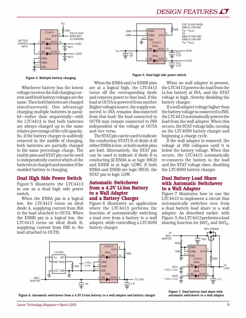
Automatic Dual Battery Load SharingA dual battery load sharing circuit is shown in Figure 3. In this schematic an LTC4413 is used to isolate two bat-teries, perhaps a main and a backup battery, from the load. This circuit takes advantage of the fact that it is more efficient to discharge the batter-ies in parallel than it is to discharge them sequentially.
Whichever battery has the higher voltage provides the load current until it has discharged to the voltage of the other battery. The load is then shared between the two batteries according to the capacity of each battery. The higher capacity battery provides proportion-ally higher current to the load.
As the LTC4413 only allows current to flow in one direction, each battery is isolated from the other so that no reverse current can flow from one battery into the other. This eliminates the possibility of a potentially hazard-ous situation where one battery may uncontrollably discharge curent into the other. The STAT pin may be used to indicate whether the backup battery attached to INA is conducting, thus providing an automatic monitor to indicate when the backup battery is supplying all of the load current.
Multiple Battery ChargingFigure 4 illustrates an application of multiple battery charging using the LTC4413. In this example, one or both of the batteries can be charged from a single battery charger (not shown), regardless of the state of charge of the other battery. This circuit takes advantage of the fact that charging batteries in parallel is more efficient than charging them sequentially.
may be tied to the output as shown in Figures 6, 7 and 8.
Consider next a wall adapter, or other auxiliary supply voltage, applied to pin INB (at time B0). The voltage at INB is then ramped upwards from 0V (starting at time B1). The LTC4413 automatically senses when the voltage at INB is greater than the voltage at the output (at time B2) and reverts to supplying load current from the input applied at pin INB; disconnecting the battery from the load as the voltage at the output rises above the battery voltage at INA. At this point, the STAT pin begins to sink 9µA causing the STAT pin voltage to fall, indicating that the wall adapter at INB is now supplying load current. As the auxil-iary voltage continues to rise to 5.5V (B3) the output voltage follows the auxiliary voltage.
When the wall adapter, or auxiliary voltage, is removed (at time C0) and the voltage at INB drops to zero, the output voltage begins to ramp down as COUT discharges; at a rate depending on the load current. Once the output
voltage drops below the battery voltage (C1) the LTC4413 reverts to supplying load current from the battery. At this time the STAT pin becomes an open circuit, and the 560k resistor pulls the STAT pin voltage to VCC to indicate that the battery is now supplying load current.
As the battery voltage continues to discharge below the under voltage lock-out threshold of 1.9V (at time D0), the LTC4413 turns itself off, and the battery is disconnected from the load. The output voltage then collapses as the load discharges capacitor COUT.
A0 A1 A2 B0 B1 B2 B3 C0 C1 D0
3.48V3.5V
0V
3.48V – VRTO
0V
5.5V
3.48V2.2V (UVLO RISINGTHRESHOLD)1.9V (UVLO FALLINGTHRESHOLD)
2.2V (UVLO RISINGTHRESHOLD)1.9V (UVLO FALLINGTHRESHOLD)
0V
5.48V
VCC
0V
BATTERYCELL
AUXILIARYSUPPLY
OUTPUTTO LOAD
STAT
Figure 2. Operation waveforms of the LTC4413.
LTC4413IDEAL
2
4
3,11
1
5
10
9
6
STAT
INA OUTABACKUP
BATTERY
560k
STAT IS HIGH WHENBACKUP BATTERY ISSUPPLYING ALL OF THE LOAD CURRENT
COUT4.7F
TOLOAD
IDEALINB OUTB
MAINBATTERY
ENBA
GND
ENBB
VCC
Figure 3. Automatic dual battery load sharing with secondary battery monitor
Linear Technology Magazine • March 2005 9
DESIGN FEATURES
When the ENBA and/or ENBB pins are at a logical high, the LTC4413 turns off the corresponding diode and removes power to that load. If the load at OUTA is powered from another (higher voltage) source, the supply con-nected to INA remains disconnected from that load; the load connected to OUTB may remain connected to INB independent of the voltage at OUTA and vice versa.
The STAT pin can be used to indicate the conduction STATUS of diode A (if either ENBA is low, or both enable pins are low). Alternatively, the STAT pin can be used to indicate if diode B is conducting (if ENBA is at logic HIGH and ENBB is at logic LOW). If both ENBA and ENBB are logic HIGH, the STAT pin is logic LOW.
Automatic Switchover from a 4.2V Li-Ion Battery to a Wall Adapter and a Battery ChargerFigure 6 illustrates an application where the LTC4413 performs the function of automatically switching a load over from a battery to a wall adapter, while controlling a LTC4059 battery charger.
When no wall adapter is present, the LTC4413 powers the load from the Li-Ion battery at INA, and the STAT voltage is high, thereby disabling the battery charger.
If a wall adapter voltage higher than the battery voltage is connected to INB, the LTC4413 automatically powers the load from the wall adapter. When this occurs, the STAT voltage falls, turning on the LTC4059 battery charger and beginning a charge cycle.
If the wall adapter is removed, the voltage at INB collapses until it is below the battery voltage. When this occurs, the LTC4413 automatically re-connects the battery to the load and the STAT voltage rises, disabling the LTC4059 battery charger.
Dual Battery Load Share with Automatic Switchover to a Wall AdapterFigure 7 illustrates how to use the LTC4413 to implement a circuit that automatically switches over from a dual battery load share to a wall adapter. As described earlier, with Figure 3, the LTC4413 performs a load sharing function for BATA and BATB,
Whichever battery has the lowest voltage receives the full charging cur-rent until both battery voltages are the same. Then both batteries are charged simultaneously. One advantage charging multiple batteries in paral-lel—rather than sequentially—with the LTC4413 is that both batteries are always charged up to the same relative percentage of the cell capacity. So, if the battery charger is suddenly removed in the middle of charging, both batteries are partially charged to the same percentage charge. The enable pins and STAT pin can be used to independently control which of the batteries is charged and monitor if the enabled battery is charging.
Dual High Side Power SwitchFigure 5 illustrates the LTC4413 in use as a dual high side power switch.
When the ENBA pin is a logical low, the LTC4413 turns on ideal diode A, supplying current from INA to the load attached to OUTA. When the ENBB pin is a logical low, the LTC4413 turns on ideal diode B, supplying current from INB to the load attached to OUTB.
LTC4413IDEAL
ENBA2
4
3,11
1
5
10
9
6
ENBB STAT
GND
INA OUTABATA
1-CELL Li-Ion
665k
100k
560k
4.7F
TOLOAD
5VWALL
ADAPTER 10µF
MP1 FDR8508
IDEALINB OUTB
BATB1-CELL Li-Ion
Figure 7. Dual battery load share with automatic switchover to a wall adapter
LTC4413
IDEAL
ENBA2
4
3,11
1
5
10
9
6
ENBB
STAT
GND
INA OUTA560k
100k1-CELLLi-Ion
IDEALINB OUTB
TO LOAD
4.7F10F
VCC
ENB
Li CC
LTC4059
PROG
WALLADAPTER
BAT
GND
Figure 6. Automatic switchover from a 4.2V Li-Ion battery to a wall adapter and battery charger
LTC4413
IDEAL
ENBA2
4
3,11
1
5
10
9
6
ENBB
STAT
GND
INA OUTA
560k
LOAD1
STAT IS HIGHWHEN BAT1IS CHARGING
BAT1
BATTERYCHARGER
INPUTIDEAL
INB OUTBLOAD2
BAT2
VCC
Figure 4. Multiple battery charging
LTC4413IDEAL
ENBA2
4
3,11
1
5
10
9
6
ENBB STAT
ENBA
ENBB
GND
INA OUTA
560k
OUTA
OUTB
VIN
IDEALINB OUTB
COUT4.7µF
COUT4.7µF
CIN10F
STAT IS HIGH WHENENBA IS LOW AND VIN > VOUTAORENBA IS HIGH AND ENBB IS LOW AND VIN > VOUTA
Figure 5. Dual high side power switch

10 Linear Technology Magazine • March 2005
DESIGN FEATURES
with the addition of an automatic switchover whenever a wall adapter is applied.
When the wall adapter is con-nected, both ENBA and ENBB voltages are pulled higher than the turn-off thresholds of 550mV through a user programmable resistive divider. When this occurs, the STAT voltage falls, turning on MP1 so that the wall adapter can provide load current. If the wall adapter is disconnected, the output voltage droops until the ENBA and ENBB voltages fall through their turn-on threshold of 450mV; enabling both ideal diodes. The LTC4413 then connects the higher of BATA or BATB to the load. If the voltage at BATA is high-est, the STAT voltage rises, otherwise the STAT voltage remains low.
Automatic Switchover from a Battery to an Auxiliary Supply or to a Wall AdapterFigure 8 shows automatic switchover from a battery to either an auxiliary supply or to a wall adapter using the LTC4413. This simple circuit handles all combinations of applied power automatically.
Consider two scenarios. In the first, the auxiliary supply is not present and the battery provides load current when the wall adapter is attached. In the second, the auxiliary is present when the wall adapter is attached.
In the first case (aux supply absent), when the wall adapter is applied, the diode in the external PFET (MP1) for-ward biases pulling the output voltage above the BAT voltage and turning off the ideal diode connected between BAT and the output. This causes the STAT voltage to fall, turning on MP1 and connecting the wall adapter to the load. The load current is then provided by the wall adapter and the battery is disconnected from the load.
When the wall adapter is removed, the output voltage falls until the BAT voltage exceeds the output voltage. When this event occurs the STAT voltage rises, turning off the external
PFET, and the ideal diode between BAT and the output automatically turns on to provide power to the load.
In the second case (aux supply present), the voltage divider (R5 and R4) pull ENBA higher than its turn-off threshold, disconnecting the battery from the load, and the auxiliary supply provides the load current.
When the wall adapter is applied, the LTC4413 senses the presence of the wall adapter as the ENBB pin volt-age is pulled higher than its turn-off threshold; through resistive divider (R2 and R3). When this occurs, the auxiliary is disconnected from the load and the STAT voltage falls, turning on MP1 so that the wall adapter can provide the load current. When the wall adapter is removed, ENBB falls until the auxiliary is enabled and reverts to providing power to the load.
If the auxiliary is removed while the wall adapter is providing load cur-rent, the ENBA voltage falls, enabling the ideal diode between BAT and the output. However, if the wall adapter voltage is higher than the BAT voltage, the ideal diode between BAT and the output is reverse biased and no cur-rent flows into the battery from the wall adapter (through the LTC4413). When the wall adapter is removed, the output voltage falls until the BAT voltage exceeds the the output voltage. At this point, the ideal diode between
BAT and the output turns-on and the STAT voltage rises, disabling MP1.
When the wall adapter is discon-nected while the auxiliary supply is present, the load voltage droops to just below the auxiliary voltage at which point the auxiliary supply begins to source the load current. At this point the STAT voltage rises; disabling MP1. This causes the capacitor C1 to discharge until the ENBA turn-on threshold is reached; this allows the battery to source load current if the output voltage drops below the bat-tery voltage.
If the wall adapter is disconnected when the auxiliary supply is not pres-ent, the load voltage drops until the voltage at the ENBA pin (formed by resistive divider R2 and R3) falls below the turn-on threshold of 450mV. When this occurs, the battery is connected to the load and the STAT voltage is pulled high, disabling MP1.
ConclusionThe LTC4413 dual monolithic ide-al diode provides a simple and efficient single-IC solution for low-loss PowerPath management. This device is ideal for battery-powered portable devices. It extends battery life, sig-nificantly reduce self-heating, and reduces form-factor with its 10-lead 3mm × 3mm footprint and minimal external parts count.
LTC4413IDEAL
ENBB4
ENBA2
3,11
1
5
10
9
6
STAT
GND
INA OUTA
R2665k
R3100k
BAT
560k
C24.7µF
TOLOAD
5VWALL
ADAPTER
2.5V–5.5VAUX
ADAPTER R41000k
R5470k
C110µF
MP1 FDR8508
IDEALINB OUTB
Figure 8. Automatic switchover from a battery to an auxiliary supply or a wall adapter
For more information on parts featured in this issue, seehttp://www.linear.com/designtools
For more information on parts featured in this issue, seehttp://www.linear.com/designtools

Linear Technology Magazine • March 2005 11
DESIGN FEATURES
by Kirk Su
VPORTN
BOLD LINE INDICATES HIGH CURRENT PATH
POUT
–
+
PGND
RCLASS
PWRGD
CONTROLCIRCUITS
INPUT CURRENT LIMIT
POWER GOOD
CLASSIFICATIONCURRENT LOAD
1.237V
EN375mA
140mA
9k
16k
–
+
EN25k
SIGNATURERESISTOR
VPORTP SIGDISA
–
+–
+
SLOPECOMP
CURRENTRAMP
PVCC
GATEDRIVER
NGATE
SENSE
200kHzOSCILLATOR
UNDERVOLTAGELOCKOUT
QR
CURRENTCOMPARATOR
SHUTDOWNCOMPARATOR
SHUTDOWN
S
20mV
ITH/RUN
ERRORAMPLIFIER
VFB
SOFT-STARTCLAMP
VCCSHUNT
REGULATOR
SWITCHINGLOGIC ANDBLANKINGCIRCUIT
0.28V PVCC <VTURNON
0.3µA
PVCC
–
+
1.2V
800mVREFERENCE
Figure 1. LTC4267 block diagram
and voltage reference allowing its use in both isolated and non-isolated configurations. All this functionality is packed into a space-saving, low-profile 16-pin SSOP or DFN package.
PD Implementation Made Simple Figure 2 presents a complete PD detection and power conversion appli-cation—a testimony as to how simple a PD implementation can be. The LTC4267’s package size is the small-est in the industry, and many of the circuits that are traditionally imple-mented with external components have been folded into this device.
During detection, the Power Sourc-ing Equipment (PSE) identvifies the presence of an IEEE 802.3af-com-pliant PD by applying two voltages, measuring the corresponding current, then performing a ΔV/ΔI calculation.
IntroductionIEEE 802.3af Power over Ethernet (PoE) is a standard for delivering power over Cat-5 cables, eliminating the need for AC-adapters for equipment plugged into the Ethernet. The two major components in a PoE system are Power Sourcing Equipment (PSE), which deliver power, and Powered De-vices (PD), which receive and use the power. A PSE will not deliver power to the load unless it detects a valid signa-ture resistance, which distinguishes a compliant PD from a device that cannot receive power. Once the PD receives power, it must also convert the –48V PoE efficiently to a suitable power supply voltage. Typical PD designs employ two ICs for these tasks. An obvious way to simplify PD designs would be to integrate the interface and DC-DC conversion circuitry into a single device.
The LTC4267 reduces the complex-ity and size of a PD by combining an IEEE 802.3af-compliant PD interface with a current mode switching regula-tor. Figure 1 shows a block diagram of the device. The LTC4267 includes the 25kΩ signature resistor, classification current source, thermal overload pro-tection, signature disable and a power good signal, along with an under-volt-age lockout (UVLO) optimized for use with the IEEE-required diode bridge. The precision dual-level current limit allows the LTC4267 to charge large load capacitors and interface with legacy PoE systems. The current-mode switching regulator is designed for driving a 6V rated N-channel MOSFET and features programmable slope compensation, soft start, and constant frequency operation, minimizing noise even with light loads. The LTC4267 includes an onboard error amplifier
Simplify PoE Implementation with Complete PD Interface and Integrated Switching Regulator

12 Linear Technology Magazine • March 2005
DESIGN FEATURES
inter-operability problems. These cur-rent-limiting features are controlled by an onboard 100V, 400mA N-channel Power MOSFET and an internal sense resistor.
The LTC4267 presents a Power Good signal once the load capacitor (CLOAD in Figure 2) is charged to within 1.5V of the final value. The Power Good signal may be used to signal to the switching regulator that the PD interface has charged up the load ca-pacitor and is ready to apply power. A 3V hysteresis is included in the power good circuit, allowing the LTC4267 to operate near the current limit point without inadvertently presenting an invalid Power Good.
The thermal shutdown circuit moni-tors the die temperature, serving as an additional means of self-protecting the LTC4267 and other electronic circuitry from over-current or over-heating conditions. If such an event occurs in either the classification sequence (from the PSE probing exceeding the IEEE-mandated 75ms maximum) or in normal PD operations (from multiple turn on events), the thermal shut-down circuit protects the LTC4267 by disconnecting power to the output load and disabling the classification current until the die returns to a safe operating temperature.
Powering the LTC4267 switching regulator in the simplest case can be achieved with a dropping resistor between VPORTP and PVCC. An internal
A 25kΩ signature resistance signals the PSE that a valid PD is present and is ready to receive power. Most PD de-tection solutions require one or more external resistors to present a valid signature during detection. One of the benefits of the LTC4267 is an inter-nal, temperature-compensated 25kΩ signature resistor, which is precision trimmed to account for the series re-sistance of the input diode bridges and all parallel leakage paths. This ensures proper PD detection without the need to size external components.
Another unique feature is the Sig-nature Disable function. When the SIGDISA pin is exercised, the LTC4267 presents a 9kΩ resistance that signals the PSE not to power the PD. This feature simplifies the interface with an external power source such as a wall transformer.
Once the PSE detects the LTC4267, the PSE may classify the PD by de-tecting a range of load currents. The LTC4267 offers a simple scheme for PD classification: the PD designer programs the classification load cur-rent using a single RCLASS resistor or leaves the RCLASS pin open for class 0. During classification, the LTC4267 asserts a precision load current from the VPORTP pin through the RCLASS resistor to notify the PSE of the PD power requirements.
The IEEE 802.3af specifies the classification voltage range to be between –15.5V to –20.5V. However,
the LTC4267 is designed to remain in classification mode from –15.5V to the UVLO turn-on threshold of –36V nomi-nal. IEEE 802.3af does not require this extended classification range, but the added range aids in the PSE-PD power-up stability by maintaining a monotonically increasing V-I charac-teristic up to the turn-on voltage.
The LTC4267 provides a complete and self-contained dual-current protection without the need for any external components. The LTC4267’s unique current limit method ensures PD inter-operability with new and legacy PSEs, and unlike competing products, the LTC4267 does not de-pend on the PSE to monitor current limit. As the LTC4267 reaches the UVLO turn-on voltage and prepares to delivers power, the LTC4267 limits the inrush current to 140mA nominal until the load capacitor (CLOAD in Figure 2) charges up to within 1.5V of the final value. Once this voltage threshold is reached, the current-limit threshold switches over to 375mA nominal for the remainder of the PD operation. The dual level current limit allows legacy PSEs with limited current sourcing capability to power up the PD while allowing the PD to maximize the power utilization from an IEEE 802.3af-compliant PSE. By maintain-ing a 375mA current limit once the PD is powered up, the LTC4267 keeps the PD from depending on the PSE for current limit and avoids possible
PVCC
PWRGD
NGATE
SENSE
ITH/RUN
VFB
PGND
POUT
VPORTP
RCLASS
SIGDISA
VPORTN
LTC4267
++
RCLASS68.1Ω
1%
CLOAD5µFMIN
10k
470
100k
60.4k
PVCC
PVCC
4.7µF
320µFMIN
22nF
•
•
PA1133
PS2911
BA5516
LT4430
SBM1040
SMAJ58A
3.3V1.5A
CHASSISHD01
+
–
+
–HD01
–48VFROM
DATA PAIR
–48VFROM
SPARE PAIR
Si3440
0.1Ω
6.8k
10k0.1µF
Figure 2. A Class 2 PD with 3.3V isolated power supply

Linear Technology Magazine • March 2005 13
DESIGN FEATURES
shunt regulator maintains the sup-ply at 9.4V, providing the required voltage needed for the gate drive. The LTC4267 can also be powered with a pre-regulator and/or with a separate bias winding on a flyback transformer. Each of these methods offer improved efficiency. The shunt regulator is particularly important when using a flyback methodology since it also serves the vital function of protecting the LTC4267 PVCC pin from seeing too much voltage.
The LTC4267 switching regulator features two ways to enable operation during the initial power-up sequence. The PVCC pin includes an UVLO circuit with hysteresis, and the ITH/RUN pin serves as an enable as well as the com-pensation point for the internal error amplifier. Once the interface circuit charges the load capacitor, enable the switching regulator operation with the ITH/RUN and PVCC pin. Note that both pins must be enabled for operation to begin. The switching regulator may be disabled by either pulling the PVCC pin below the UVLO turn-off threshold or by pulling the ITH/RUN pin below the 0.28V nominal threshold.
Implementing a robust power-up sequence between the PD Interface circuit and the switching regulator is critical in a successful PD applica-tion. The power good signal indicates that the load capacitor is charged and this signal can be used to enable
the switching regulator. An N-chan-nel transistor driven by PWRGD can be used to disable the switcher by clamping the PVCC or ITH/RUN pins. Disabling the switching regulator until the load capacitor is charged up can also be accomplished with an RC delay on the PVCC pin as shown in Figure 2. The flexibility of the LTC4267 provides the PD designer with the freedom of implementing a controlled power-up sequence in a variety of ways.
The LTC4267 features a soft-start feature that provides an additional 1.4ms delay once the ITH/RUN pin is re-leased. The soft-start feature reduces the switching regulator inrush current and reduces output overshoots. Unlike competing products, there is no mini-mum external capacitance required to program this delay. The designer may opt to provide additional soft-start de-lay by employing an external capacitor between ITH/RUN and PGND pins.
An internal error amplifier with a precision voltage reference is integrat-ed into the LTC4267. This feature is particularly desirable in non-isolated power supply applications since the PD designer does not need to add an external amplifier or reference. The internal precision reference provides output voltage accuracy to within ±1.5% over the 0oC to 70oC tempera-ture range. For isolated power supply applications, the internal error ampli-fier and reference can be disabled by
connecting the VFB pin to PGND, and connecting an external error ampli-fier and opto-isolator to the ITH/RUN pin. Figure 2 shows an example of an isolated power supply using an external amplifier and Figure 3 shows a non-isolated supply that uses the LTC4267’s internal error amplifier.
Slope compensation is critical for stabilizing the control loop against sub-harmonic oscillations and is avail-able on the LTC4267 by including an optional resistor between the sense resistor and the SENSE pin of the LTC4267. The SENSE pin monitors the voltage across the sense resis-tor. It also sources 5µA through the slope compensation resistor, raising the SENSE pin voltage above the sense resistor voltage. This in turn amends the duty cycle of the switching regulator, preventing sub-harmonic oscillation.
ConclusionThe LTC4267 is a self-contained Power over Ethernet PD interface that com-bines 802.3af PD classification with a switching regulator. It integrates many features that are traditionally implemented with separate compo-nents, but it retains the flexibility that external components offer. The result is a compact, easy-to-use, but versatile device.
PVCC
NGATE
PWRGD
SENSE
VFB
ITH/RUN
VPORTP
RCLASS
SIGDISA
VPORTN
LTC4267
45.3Ω1%
100k
1µF
300µF**
•
•
COILTRONICSCTX-02-15242
BAS516
UPS840
SMAJ58A
5V1.8A
HD01
HD01
+
–
+
–
–48VFROM
DATA PAIR
–48VFROM
SPARE PAIR
FDC2512
0.04Ω1%
10k
220k
220Ω
42.2k1%
27k
150pF200V
9.1V
22nF
0.1µF
5µF*MIN
PGNDPOUT
MMBTA42
8.06k1% *1µF CERAMIC + 4.7µF TANTALUM
** THREE 100µF CERAMICS
Figure 3. A Class 3 PD with 5V non-isolated power supply

14 Linear Technology Magazine • March 2005
DESIGN FEATURES
IntroductionCrystal based oscillators are often the default choice for designers looking to clock today’s high speed microcontrollers, data converters and programmable logic devices. Crystal oscillators, although convenient, accu-rate and stable, come at a high price in use—they occupy considerable board space, consume significant power, and are sensitive to environmental factors like shock and temperature extremes. The LTC6905 is an all silicon clock that avoids these pitfalls, making it an alternative to crystal oscillators in applications up to 170MHz.
Accuracy and jitter specifications of the LTC6905 are more than sufficient for most applications, and its power and size advantages allow the LTC6905 to fit in designs where a crystal oscil-lator could never go.
Device DescriptionThe LTC6905 is a part of Linear Technology’s line of resistor controlled SOT-23 oscillators. These resistor controlled oscillators use a single external resistor to accurately set the oscillator frequency, and there is a simple linear relationship between the resistor value and the frequency (see Figure 1). The LTC6905 is pin-compatible with the LTC1799 SOT-23 oscillator, but uses a different control resistor range and a different formula to set the frequency.
The LTC6905 is also available in fixed frequency versions, where the resistor is internal to the part and no external components other than a bypass capacitor are required. Preset devices with master oscillator frequen-cies of 133MHz, 100MHz, 96MHz and 80 MHz and 1.5% accuracy are avail-able. These devices have an internal divider which makes it possible to produce most popular frequencies between 20MHz and 133MHz. Devices can be customized to output any
frequency in the range of 2.2MHz to 170Mhz.
The LTC6905 uses an internal feedback loop to accurately match the impedance of a switched capacitor element to the external resistor con-nected to the RSET pin, thus setting the master oscillator frequency. The voltage level on the DIV pin engages internal dividers to divide this master frequency by 1, 2 or 4 before it is sent to the OUT pin. With fixed frequency devices, the LTC6905-XXX series of parts, the RSET pin is replaced by an output enable pin, which disables the output when it is connected to GND.
The voltage on the RSET pin of the LTC6905 is forced to a bandgap controlled voltage of 1V below the positive supply, independent of the temperature or supply voltage, with a tolerance of less than 5%. This stable RSET voltage makes the LTC6905 ideal for applications where an accurate voltage or current controlled frequency is required.
The frequency range of the master oscillator in the LTC6905 is limited to between 70MHz and 170MHz, which corresponds to external frequency setting resistor values between 10kΩ and 25kΩ. This range is expanded by the internal dividers to between 17MHz and 170MHz, and is limited by the architecture of the high speed master oscillator.
The master oscillator of the LTC6905 is a voltage controlled ring oscillator, and provides a unique jitter profile where the jitter percent-age remains relatively constant over
High Accuracy Clock up to 170MHz in a SOT-23
frequency. Traditional relaxation oscil-lators develop a larger percentage jitter as the frequency increases. The jitter of the LTC6905 actually decreases with increasing operating frequency, making it ideal for high frequency applications.
Fixed Frequency DevicesThe LTC6905 can be ordered in a fixed frequency version where the frequency-setting resistor is inside the part. An output enable pin is made available in place of the RSET pin on these devices only. Four versions are available: LTC6905-133, LTC6905-100, LTC6905-96 and LTC6905-80. These four versions collectively offer 12 popular frequencies through the use of their DIV pins. Please see Table 1.
The LTC6905-XXX fixed frequency oscillators offer several advantages that stem from their internal resis-tor configuration. The parts are less sensitive to external noise that may couple into the RSET pin on the external resistor version of the part. This lack of sensitivity translates into improved jitter of less than 1% at all frequencies and accuracy of better than 1.5% over commercial temperature range. The in-ternal resistor parts are generally more accurate because they are trimmed at one specific frequency and do not have any error term from nonlinearities over the RSET resistor range.
The absence of an RSET pin on the fixed-frequency devices has made room for an output enable pin. This output enable synchronously disables the output drivers when brought low,
by Albert Huntington
V+1
2
3
5
17.225MHz ≤ fOSC ≤ 170MHz5V
5V10k ≤ RSET ≤ 25k0.1µF
4
GNDLTC6905
SET
OUT
DIV OPEN÷2
÷1
÷4
Figure 1. A single resistor sets the frequency of this tiny, robust oscillator.

Linear Technology Magazine • March 2005 15
DESIGN FEATURES
the LTC6905, it is strongly recom-mended that the connection between the capacitor and the LTC6905 be as short as possible and use multiple, filled vias to minimize series induc-tance and resistance.
The LTC6905 is specified at an output load of 5pF, which is equiva-lent to about two standard HC logic inputs. Driving this load at 170MHz is the single largest factor in the power consumption of the LTC6905. The power supply current needed to drive a capacitive load may be calculated as: ISUPPLY = CLOAD • VSWING • FOSC
where CLOAD is the 5pF load capaci-tance, VSWING is the voltage swing, in this case up to 5.5V, and FOSC is the frequency of the oscillator. Driving a 5.5V swing into a 5pF load at 170MHz takes 4.675mA on average.
The majority of this power is expended during the risetime and falltime of the output signal, not while it is in a steady state. The 500ps rise and fall times of the LTC6905 mean that the instantaneous power supply current required during the rise and fall portions of the waveform is much greater than the average. The instan-taneous power supply current may be calculated by a similar formula:
IPEAK = CLOAD × VSWING × 1
trf
where trf is the rise/fall time of the signal. In this case, 55mA spikes are
and does not produce pulse slivers. Power dissipation is significantly reduced because much of the power is dedicated to driving output capaci-tance. The internal master oscillator and bias networks remain active in order to facilitate an immediate and accurate frequency output when the output is enabled. If the output en-able pin is left floating or pulled to the positive supply, the oscillator is enabled.
Layout ConsiderationsBecause the LTC6905 combines a high frequency oscillator and output stage with a sensitive analog control loop, it is necessary to exercise great care in board layout to maximize accuracy and stability. The bypass capacitor must be placed as close as possible to the LTC6905, preferably on the same side of the board. Even the small inductance and resistance of vias in the pc board can adversely effect part performance. Additionally, the traces to the bypass capacitor should be larger than is indicated by the power consumption of the device. Although the average power consumption is low, driving a capacitively loaded output will induce spikes in the supply cur-rent which must be damped by the bypass capacitor.
The RSET pin is the most sensitive input pin, and attempts must be made to shield it from noise coupling or excessive parasitic capacitance. It is recommended that the frequency setting resistor be located as close as possible to the RSET pin, and that the frequency setting resistor be connected to the positive supply as close as pos-sible to the V+ pin. A recommended layout is illustrated in Figure 2. If the bypass capacitor must be situated on the opposite side of the PC board from
generated by driving 5.5V into a 5pF load.
Because of these power supply spikes, and because of the tendency for fast edges to couple into adjacent lines, the layout of the output trace is critical. Capacitance, trace length and loading should be minimized. Ad-ditionally, with traces longer than a few centimeters, transmission line effects must be taken into consideration.
Should output loading and coupling problems occur, there are methods to mitigate the effects. A series resistance in the range of 50Ω–1000Ω placed adjacent to the output pin of the device will increase the rise and fall times of the signal being driven into the output load, and therefore reduce power supply spikes and coupling (see Figure 3). A 50Ω cable may be driven using a 950Ω series resistance and a 50Ω termination to ground, though the signal will be attenuated (see Figure 4). A high speed comparator or inexpensive AHC series CMOS logic gate may be placed in the signal path directly after the LTC6905 in order to buffer the output signal and drive heavier loads.
Voltage and Current Controlled OscillatorsThe LTC6905 is an ideal candidate for making a voltage or current con-trolled oscillator. Unlike other resistor controlled parts, where the voltage on RSET varies with power supply and temperature, the LTC6905 maintains
Table 1. LTC6905 family fixed frequency oscillators
DIV Setting LTC6905-133 LTC6905-100 LTC6905-96 LTC6905-80
V+ (÷1) 133.33MHz 100 MHz 96 MHz 80 MHz
OPEN (÷2) 66.66MHz 50MHz 48MHz 40MHz
GND (÷4) 33.33MHz 25MHz 24MHz 20MHz
V+1
2
3
5V+
950Ω 50Ω CABLE
50ΩV+0.1µF
4
GNDLTC6905
SET
OUT
DIV
Figure 4. The LTC6905 can drive a 50Ω cable with appropriate termination.
LTC6905
CR
Figure 2. LTC6905 Suggested layout. Note that the bypass capacitor is located adjacent to the device and on the same side of the PC board.
V+1
2
3
5V+
100Ω
V+
0.1µF CLOAD
4
GNDLTC6905
SET
OUT
DIV
Figure 3. A series resistor on the LTC6905 output pin reduces power supply spikes caused by load capacitance.
continued on page 38

16 Linear Technology Magazine • March 2005
DESIGN FEATURES
IntroductionThe LTC®6915 is the simplest, most precise way to obtain digitally pro-grammable voltage gain. Any system which needs accurate amplification of small differential voltages and rejec-tion of large common mode signals will benefit from the LTC6915.
The LTC6915 is an evolution of the LTC2053, a precision rail-to-rail input and output, zero-drift instrumentation amplifier. Due to the amplifier’s very low DC errors, very high levels of gain can be taken in a single stage. The LTC2053 uses external resistors to set the gain; the LTC6915 uses a serial port or a parallel port to select internal resistors, and therefore select the gain. The gain can be programmed to 0, 1, 2, 4, 8, 16, 32, 64, 128, 256, 512, 1024, 2048, or 4096. Programmable gain increases the dynamic range of any system. A fixed gain instrumentation amplifier would have about 60dB of useful range. The dynamic range of the LTC6915 is more than 120dB.
Since the high CMRR (typically 125dB) is independent of the gain set-ting, microvolts of differential signal can be extracted from volts of common mode noise. Furthermore, the common mode level of the differential signal can be any value within the supply rails of the LTC6915.
Other features of the LTC6915 include a flexible digital interface, a Kelvin connected output stage, a wide supply range, a shutdown mode, and a choice of packages.
How it WorksFigure 1 shows a block diagram of the LTC6915. A sophisticated, charge bal-anced sampling technique impresses the differential input voltage on to a 1000pF internal capacitor. The dif-ferential input signal is converted to a single-ended signal referenced to
an integrated precision resistor ladder. For gains up to 1024V/V, the accuracy is guaranteed to be better than ±0.6% over temperature (Figure 2), with a typical gain drift of less than 2ppm. A
the “REF” pin of the LTC6915. This single-ended signal is then amplified by a zero-drift op amp connected as a non-inverting gain stage. With OUT connected to SENSE, the gain is set by
Simple, Precise Instrumentation Amplifier Features Digitally Programmable Gains from 1 to 4096
by Michael Kultgen
Figure 1. The LTC6915 block diagram. The small GN16 package (a) has all control features. The DFN12 package version (b) sacrifices the shutdown and data latching control features for even smaller size.
–
+
RESISTORARRAY
MUX 4-BITLATCH
Q0 Q1 Q2 Q3 Q4 Q5 Q6 Q78-BIT
SHIFT-REGISTER
HOLD_THRU
CS(D0)DIN(D1)
CLK(D2)
DOUT(D3)
PARALLEL_SERIAL
IN–
IN+ 3
2
11
67
8
9
CS CH
V+
V–
SHDN
DGND
13
5
16
10
1
4
OUT
REF
15
14CF
SENSE
GAINCONTROL
–
+
RESISTORARRAY
MUX 4-BITLATCH
Q0 Q1 Q2 Q3 Q4 Q5 Q6 Q78-BIT
SHIFT-REGISTER
CS(D0)DIN(D1)
CLK(D2)
DOUT(D3)
PARALLEL_SERIAL
IN–
IN+ 2
1
9
45
6
7
CS CH
V+
V–
DGND
DGND
10
12
8
3
OUT
REF
11
CFGAIN
CONTROL
a. The LTC6915 in a GN16 Package
b. The LTC6915 in a DFN12 Package

Linear Technology Magazine • March 2005 17
DESIGN FEATURES
using the falling edge of the clock to output data, the LTC6915 is im-mune to the slow rise and fall times often encountered in optically isolated interfaces. But that does not imply that the LTC6915 is slow. When the DOUT timing is unimportant, data can be input to the LTC6915 as fast as 10MHz!
The internal shift register is eight bits wide; the four LSBs set the gain, and the four MSBs are ignored. This simplifies some software designs be-
3kHz sampling rate means that signals from DC to 1.5 kHz can be amplified by the LTC6915.
The LTC6915 has the outstanding DC precision inherent in all of Linear Technology’s zero-drift amplifiers. The room temperature DC offset is less than ±10µV with less than ±50nV/°C of drift. The 10nA maximum input bias current means there is no additional DC error from source impedances up
to 10kΩ. The high CMRR and PSRR make the LTC6915 immune to fluc-tuations in power supplies or common mode levels.
The LTC6915 has both a parallel and serial digital interface. Its unique logic design makes it possible to guar-antee input high and low thresholds (VIH/VIL) of 2.0 and 0.8 volts for any power supply voltage from 2.7V to ±5.5V. Therefore, microprocessors or FPGAs running on a 2.5V supply can directly interface to the LTC6915 without restriction. The LTC6915 sup-ply can be a single 2.7V up to a split ±5.5V supply without additional level shifting of the digital inputs.
Versatile Serial ControlConnecting the PARALLEL/ S E R I A L pin to V– puts the LTC6915 in serial control mode. The chip select (CS), clock (CLK), and DATA pins form a simple 3-wire serial input (Figure 3). For daisy chaining (Figure 4), there is also a data out (DOUT) pin. By
SHDN
IN–
IN+
V–
HOLD_THRU
CS(D0)
DIN(D1)
CLK(D2)
V+
OUT
SENSE
REF
NC
P/S
DGND
DOUT(D3)
LTC6915#2
VOUT
DOUT
0.1µFSHDN
IN–
IN+
V–
HOLD_THRU
CS(D0)
DIN(D1)
CLK(D2)
V+
OUT
SENSE
REF
NC
P/S
DGND
DOUT(D3)
LTC6915#1
VOUT
0.1µF0.1µF0.1µF
0.1µF
µP
–5V –5V
–5V
0.1µF
–5V
CS
DIN
CLK
CLK
DIN
CS/LD
D15 D11 D10 D9 D8 D7 D3 D2 D1 D0
GAIN CODE FOR #2 GAIN CODE FOR #1
VIN VIN
GAIN CODE 0000 0001 0010 0011 0100 0101 0110 0111 1000 1001 1010 1011 1100 1101-1111
GAIN 0 1 2 4 8 16 32 64 128 256 512 1024 2048 4096
Figure 4. Two LTC6915s can be connected in a daisy chain. The binary codes for each gain setting are also shown.
4-BIT GAINCONTROL CODE
4-BITLATCH
Q0 Q1 Q2 Q3 Q4 Q5 Q6 Q78-BIT
SHIFT-REGISTER
DOUT(D3)CLK
DIN
CS
Figure 3. The LTC6915 uses a simple and standard 3-wire serial interface.
GAIN
ERR
OR (%
)
GAIN SETTING (V/V)10K1
1.5
-1.510 100 1k
-1
-0.5
0.5
0
1 MIN/MAX OF1000 UNITS
DATASHEET LIMITSMEAN OF1000 UNITS
Figure 2. The gain accuracy of the LTC6915 is typically better than 0.5%.

18 Linear Technology Magazine • March 2005
DESIGN FEATURES
cause the LTC6915 appears to be a “byte wide” device, though it is still an option to load four bits at a time.
Simple Parallel ControlThe gain can also be set by simple pin strapping, or through the use of a few spare I/O signals. Just connect the PARALLEL/ SERIAL pin to V+ and put the LTC6915 in parallel control mode. Four inputs (D3, D2, D1, D0) directly set the gain of the amplifier as also shown in Figure 4. There is even the ability to “latch” the parallel control bits into the LTC6915 using the HOLD/THRU pin (GN16 package). When this pin goes high, whatever sig-nals are present on D3…D0 are latched into the LTC6915. Any changes in D3 to D0 are ignored until HOLD/THRU is brought low again.
A Flexible OutputThe SENSE pin allows clever im-provements in the load driving or multiplexing ability of the LTC6915. In Figure 5 a discrete NPN transistor is added to increase the load driving ability. The SENSE pin is Kelvin con-nected to the load. Gain errors from the VBE of the NPN and the IR drop in the interconnect are eliminated. A precise voltage is delivered to the load. Pin-strapping is used to fix the gain of the amplifier to Code 1011, for a gain of 1024, using the parallel interface option.
In Figure 6 two LTC6915s are con-nected as a multiplexer. One device is programmed for a gain of 0 (three-stated output) while the other device is programmed for a gain ≥1. Using
the serial interface, the gain change of one amplifier, and disabling of the other occurs simultaneously when the CS makes a low to high transition. As a precaution for output shorting,
200Ω resistors are in series with each output in case both amplifiers are ever on simultaneously. The SENSE pin eliminates any error due to the IR drop in the 200Ω resistor during normal operation.
In Figure 7 a software program-mable current sink is created using the SENSE pin, an external MOSFET, and the internal gain network. This design can sink a wide range of currents, 0µA to 40.96mA, due to the precision of the internal zero-drift amplifier and the wide range of gain settings. With only 10µV maximum offset voltage error, the circuit operates with an input reference voltage of only 250µV to 500µV. The reference voltage is set by a small regulated current—fixed by the 400mV reference voltage of an
LTC6915
V+
5V TO 11V
0 TO 40.96mA
4.99k
10k
RIN5Ω
ROUT49.9Ω
OUTIN
FB
LT6650
BINARYCODE0 TO 13
LOAD
1M
40µA TO 120µA
250µV TO500µV
+
–
N VN2222L
Figure 7. A wide range programmable precision current source takes advantage of the precision of the zero-drift amplifier topology.
SHDN
IN–
IN+
V–
HOLD_THRU
CS
DIN
CLK
V+
OUT
SENSE
REF
NC
P/S
DGND
DOUT
LTC6915#1
–5V
–5V
µP(TTL
LEVELS)
DATA
SELECT
CLOCK
0.1µF
0.1µF
5V
VIN1
SHDN
IN–
IN+
V–
HOLD_THRU
CS
DIN
CLK
V+
OUT
SENSE
REF
NC
P/S
DGND
DOUT
LTC6915#2
–5V
–5V
0.1µF
0.1µF
5V
VIN2VOUT
200 200
Figure 6. A robust variable gain multiplexer using the high impedance 0 gain setting allows very wide dynamic range in multichannel systems.
0.1µF
5V
SHDN
IN–
IN+
V–
HOLD_THRU
CS(D0)
DIN(D1)
CLK(D2)
V+
OUT
SENSE
REF
NC
P/S
DGND
DOUT(D3)
LTC6915
VOUT
RLOAD
INTERCONNECTRESISTANCE
5V
5V
VIN1
2N304
Figure 5. Kelvin sensing at the output maintains precision with increased load drive.

Linear Technology Magazine • March 2005 19
DESIGN FEATURES
LT6650—flowing through a 5Ω input resistor. This small voltage is ampli-fied by the programmed gain of the LTC6915 and forces a current to flow through the 50Ω output resistor via the MOSFET. The voltage compliance of the current sink is determined by the maximum voltage output to the SENSE pin. In this example, the maxi-mum output voltage is only 2.048V, required when the input reference is 500µV and the gain is 4096.
Each successive control code to the LTC6915 increases the output current by a factor of two. Any current level between the binary weighted intervals is achieved by adjusting the input
reference voltage. A gain of 1 provides an output current of 5µA to 10µA, and a gain of 4096 outputs 20.48mA to 40.96mA, with better than ±1% typical linearity.
Bridge Amplifier ApplicationThe LTC6915 is ideal for current sensing, thermocouple amplifiers, strain gauges, and many other low fre-quency and close-to-DC applications. The internal op amp gain bandwidth product is 200kHz with a slew rate of 0.2V/µs and the response time to 0.1% accuracy to a step change in gain can vary between 4ms and 15ms. Figure 8 shows the LTC6915
amplifying a bridge sensor. When in standby the circuit draws less than 100µA. An interrupt to the processor initiates a measurement cycle, turn-ing on the LTC6915 and acquiring a conversion result from the LTC2431 A/D converter.
ConclusionThe LTC6915 instrumentation ampli-fier combines outstanding precision analog performance with a flexible digital interface. The result is a soft-ware programmable gain stage which is precise and easy to use.
SHDN
IN–
IN+
V–
HOLD_THRU
CS(D0)
DIN(D1)
CLK(D2)
SDO
SCK
CS
FO
REF+
REF–
IN+
IN–
V+
OUT
SENSE
REF
NC
P/S
DGND
DOUT(D3)
LTC6915#1
C50.1µF
C20.1µF
C10.1µF
0VMEASURE STANDBY
V+
V+
V+
V+
V+
V+
CONTROL SIGNAL10k
17
16
15
14
13
12
11
28
27
26
25
24
23
22
21
7
6
5
4
3
2
X14MHz
9
10
1
VSS VSS
8 19
BRIDGESENSOR
R < 10K
20
18
10k
LT1790-1.25
VIN VOUT
GND1 GND2
C30.1µF
C31µF
ZETEXZXM61P02F
VCC
GND
LTC2431
MOSI
MISO
SCLK
CS1
CS2
RC6/TX/CK
RC5/SDO
RC4/SDI/SDA
RC3/SCK/SCL
RC2/CCP1
RC1/T1OSI/CCP2
RC0/T1OSO/T1CK1
RC7/RX/OT
OSC1/CLKIN
OSC2/CLKOUT
MCLR/VPP
RB7
RB6
RB5
RB4
RB3
RB2
RB1
RB0/INT
RAS/AN4/SS
RA4/T0CLK1
RA3/AN3/VREF–
RA2/AN2
RA1/AN1
RA0/AN0
D1BAV74LT1SOT-23
R11k
VDD
PIC16LF73
1.25V
Figure 8. Using the LTC6915 as a direct bridge amplifier in a measurement system with very low standby current

20 Linear Technology Magazine • March 2005
DESIGN FEATURES
Flexible Power Supply Sequencing and Monitoring by Jeff Heath and Akin Kestelli IntroductionThe LTC2924 is a complete power sup-ply sequencer and supervisor solution for multivoltage-rail systems, such as telecommunications equipment, memory modules, optical systems, networking equipment, servers, and base stations. The FPGAs and other digital ICs used in these applications
OUT1
OUT2
OUT3
OUT4
ON
DONE
FAULT
TMR
PGT
IN1
IN2
IN3
IN4
HYS/CFG
VCC
GND
LTC2924
150nF
SYSTEMCONTROLLER
150nF
POWER SUPPLY 4
POWER SUPPLY 3
POWER SUPPLY 2
POWER SUPPLY 1VON 3.01VVOFF 2.68V
VON 4.49VVOFF 3.99V
VON 1.43VVOFF 1.27V
VON 2.25VVOFF 2V
33.2k
9.31k
24.9k
0.1µF
15.8k 49.9k
11.81k 7.87k 8.45k
49.9k
2.5VSHDN
1.6VSHDN
5VSHDN
3.3VSHDN
10k
5V EARLY*
10k
*5V EARLY MUST BE ON BEFORESEQUENCING SUPPLIES
Figure 1b. Similar application to Figure 1a, but control is via the converter shutdown pins
OUT1
OUT2
OUT3
OUT4
ON
DONE
FAULT
TMR
PGT
IN1
IN2
IN3
IN4
HYS/CFG
LTC2924
VCC
GND150nF
SYSTEMCONTROLLER
150nF
0.1µF
0.1µF
0.1µF
0.1µF
11.8k
52.3k
0.1µF
Q4
Q3
Q2
Q1
45.3k 6.04k 1.62k
7.68k 1.69k
Q1-Q4: IRL3714SALL RESISTORS 1%
3.09k
VON = 0.93VVOFF = 0.91V
VON = 2.79VVOFF = 2.73V
VON = 4.21VVOFF = 3.76V
VON = 3.32VVOFF = 2.80V
49.9k
10k
5VEARLY
10k
5V
3V
1V
Figure 1a. Typical 4-supply sequencer using external N-channel MOSFETs for voltage control
require multiple voltage rails that must start up and shut down in a specific order, otherwise the ICs can be damaged. The LTC2924 is a simple and compact solution to power supply sequencing in a 16-pin SSOP package (see Figure 1).
Sure, alternative sequencing solu-tions are available, but few, if any, can
match the ease-of-use, space-saving design, flexibility, and cost effective-ness of the LT2924. For instance, solutions that use discrete components incur a challenging and time-consum-ing design effort to interface with the digital system, and consume a sig-nificant amount of board real estate. Another option, an integrated power supply sequencer, is more expensive and consumes more board space than any LTC2924-based solution, and may require proprietary software and the programming of complicated digital registers. Neither of these options comes close to offering the flexibility across applications that the LTC2924 does. It can be used out-of-the-box, with a few external components, to sequence and supervise just about any type of power supply, converter, or power module.
How it WorksFour power supplies can be easily sequenced using a single LTC2924, and multiple LTC2924s can be just as easily cascaded to sequence any number of power supplies. With slightly reduced functionality, six power supplies can be sequenced with a single LTC2924 (see Figure 5 and “Sequencing Six Supplies with a Single LTC2924” in this article).
The LTC2924 controls the start-up and shutdown sequence, and ramp rates, of four power supply channels via output pins (OUT1–OUT4). Each OUT pin uses a 10µA current source connected to an internal charge pump and a low resistance switch to GND. This combination makes the outputs flexible enough to connect them di-rectly to power supply shutdown pins, or to external N-Channel MOSFET switches. Figure 1a illustrates a typi-cal application for the LTC2924 where four supplies are sequenced using external N-channel MOSFETs, and Figure 1b shows a comparable circuit with four power supplies sequenced using their shutdown pins.
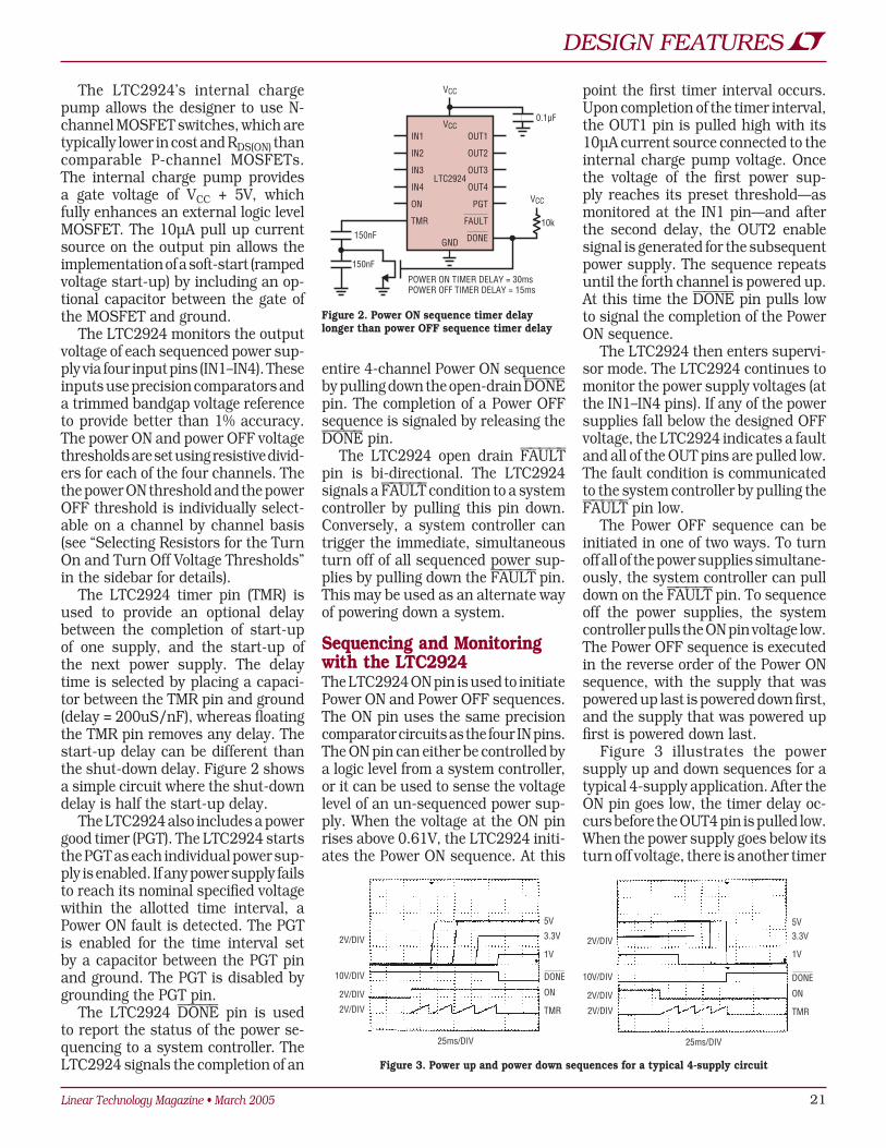
Linear Technology Magazine • March 2005 21
DESIGN FEATURES
The LTC2924’s internal charge pump allows the designer to use N-channel MOSFET switches, which are typically lower in cost and RDS(ON) than comparable P-channel MOSFETs. The internal charge pump provides a gate voltage of VCC + 5V, which fully enhances an external logic level MOSFET. The 10µA pull up current source on the output pin allows the implementation of a soft-start (ramped voltage start-up) by including an op-tional capacitor between the gate of the MOSFET and ground.
The LTC2924 monitors the output voltage of each sequenced power sup-ply via four input pins (IN1–IN4). These inputs use precision comparators and a trimmed bandgap voltage reference to provide better than 1% accuracy. The power ON and power OFF voltage thresholds are set using resistive divid-ers for each of the four channels. The the power ON threshold and the power OFF threshold is individually select-able on a channel by channel basis (see “Selecting Resistors for the Turn On and Turn Off Voltage Thresholds” in the sidebar for details).
The LTC2924 timer pin (TMR) is used to provide an optional delay between the completion of start-up of one supply, and the start-up of the next power supply. The delay time is selected by placing a capaci-tor between the TMR pin and ground (delay = 200uS/nF), whereas floating the TMR pin removes any delay. The start-up delay can be different than the shut-down delay. Figure 2 shows a simple circuit where the shut-down delay is half the start-up delay.
The LTC2924 also includes a power good timer (PGT). The LTC2924 starts the PGT as each individual power sup-ply is enabled. If any power supply fails to reach its nominal specified voltage within the allotted time interval, a Power ON fault is detected. The PGT is enabled for the time interval set by a capacitor between the PGT pin and ground. The PGT is disabled by grounding the PGT pin.
The LTC2924 DONE pin is used to report the status of the power se-quencing to a system controller. The LTC2924 signals the completion of an
entire 4-channel Power ON sequence by pulling down the open-drain DONE pin. The completion of a Power OFF sequence is signaled by releasing the DONE pin.
The LTC2924 open drain FAULT pin is bi-directional. The LTC2924 signals a FAULT condition to a system controller by pulling this pin down. Conversely, a system controller can trigger the immediate, simultaneous turn off of all sequenced power sup-plies by pulling down the FAULT pin. This may be used as an alternate way of powering down a system.
Sequencing and Monitoring with the LTC2924The LTC2924 ON pin is used to initiate Power ON and Power OFF sequences. The ON pin uses the same precision comparator circuits as the four IN pins. The ON pin can either be controlled by a logic level from a system controller, or it can be used to sense the voltage level of an un-sequenced power sup-ply. When the voltage at the ON pin rises above 0.61V, the LTC2924 initi-ates the Power ON sequence. At this
point the first timer interval occurs. Upon completion of the timer interval, the OUT1 pin is pulled high with its 10µA current source connected to the internal charge pump voltage. Once the voltage of the first power sup-ply reaches its preset threshold—as monitored at the IN1 pin—and after the second delay, the OUT2 enable signal is generated for the subsequent power supply. The sequence repeats until the forth channel is powered up. At this time the DONE pin pulls low to signal the completion of the Power ON sequence.
The LTC2924 then enters supervi-sor mode. The LTC2924 continues to monitor the power supply voltages (at the IN1–IN4 pins). If any of the power supplies fall below the designed OFF voltage, the LTC2924 indicates a fault and all of the OUT pins are pulled low. The fault condition is communicated to the system controller by pulling the FAULT pin low.
The Power OFF sequence can be initiated in one of two ways. To turn off all of the power supplies simultane-ously, the system controller can pull down on the FAULT pin. To sequence off the power supplies, the system controller pulls the ON pin voltage low. The Power OFF sequence is executed in the reverse order of the Power ON sequence, with the supply that was powered up last is powered down first, and the supply that was powered up first is powered down last.
Figure 3 illustrates the power supply up and down sequences for a typical 4-supply application. After the ON pin goes low, the timer delay oc-curs before the OUT4 pin is pulled low. When the power supply goes below its turn off voltage, there is another timer
IN1
IN2
IN3
IN4
ON
TMR
OUT1
OUT2
OUT3
OUT4
PGT
FAULT
DONE
VCC
VCC
GND
LTC2924
150nF
0.1µF
150nF
POWER ON TIMER DELAY = 30msPOWER OFF TIMER DELAY = 15ms
VCC
10k
Figure 2. Power ON sequence timer delay longer than power OFF sequence timer delay
2V/DIV
5V
3.3V
1V
DONE
ON
TMR
10V/DIV
2V/DIV
2V/DIV
25ms/DIV
2V/DIV
5V3.3V
1V
DONE
ON
TMR
10V/DIV
2V/DIV
2V/DIV
25ms/DIV
Figure 3. Power up and power down sequences for a typical 4-supply circuit

22 Linear Technology Magazine • March 2005
DESIGN FEATURES
delay. The sequence repeats until the final power supply has powered down. The LTC2924 signals the end of the Power OFF sequence by releasing the DONE pin.
Cascading the LTC2924 for Eight Supplies and UpTwo or more LTC2924s can be cas-caded to fully sequence eight or more supplies. The smart configuration logic in the LTC2924 makes the job of cascading multiple LTC2924 ICs easy. Figure 4 shows three devices configured to sequence 12 supplies. To set the sequence of each of the LTC2924 ICs, the HYS/CFG, DONE, and ON pins are connected as shown. See the LTC2924 data sheet for op-erational details. To sequence more
than 12 power supplies, simply add more LTC2924 ICs in the middle, or 2nd position, in Figure 4. To sequence up to eight power supplies remove the LTC2924 in the middle position.
Sequencing Six Supplies with a Single LTC2924Figure 5 shows how to sequence six supplies with one LTC2924. When the system controller releases the TURN OFF node, the first power supply turns on. The ON pin is tied to the output of the first power supply. Once this power supply is powered on, the LTC2924 sequentially starts up power supplies 2 through 5. When the DONE pin is pulled low after the 5th power supply powers ON, the inverted signal allows the 6th power supply to turn on. This inverter can be implemented with a single transistor. The system controller can power off all six power supplies simultaneously by pulling the TURN OFF node low.
Delayed Remote Sensing Remote sensing is a common configu-ration in high current applications. Parasitic resistances in the power supply path coupled with high DC currents can result in unacceptable DC voltage drops. The sense pin of a power module is designed to regu-late the DC voltage at a point in the power distribution circuitry beyond the parasitic resistance to compensate for the I • R voltage drop. The output voltage of the power module is raised until the desired voltage is reached at sense point.
The problem with this feedback scheme is that many power modules have unalterable maximum output voltages, which, if exceeded, cause the power supply to shut down. This limits the amount of voltage correction available to compensate for parasitic
OUT1
OUT2
OUT3
OUT4
DONE
FAULT
ON
IN1
IN2
IN3
IN4
LTC2924
VCC
GND
SHDN VOUT
PS1
SHDN VOUT
PS2
SHDN VOUT
PS3
SHDN VOUT
PS4
SHDN VOUT
PS5
SHDN
*VCC EARLY MUST BE ON BEFORESEQUENCING SUPPLIES
VOUT
PS6
TURN OFF
VCC EARLY*
SYSTEMCONTROLLER
Figure 5. A 6-supply sequencer
TMR
HYS/CFG
ON
IN1
IN2
IN3
IN4
VCC
GND
PGT
OUT1
OUT2
OUT3
OUT4
DONE
LTC2924
VCC
FAULT
VCC
VCCDONE
10k
10k
FAULT
TMR
HYS/CFG
ON
IN1
IN2
IN3
IN4
VCC
GND
PGT
OUT1
OUT2
OUT3
OUT4
DONE
LTC2924
RHYS RHYS
FAULT
TMR
HYS/CFG
ON
IN1
IN2
IN3
IN4
VCC
GND
PGT
OUT1
OUT2
OUT3
OUT4
DONE
LTC2924ONRHYS
FAULT
Figure 4. Cascading LTC2924 ICs to sequence 12 power supplies

Linear Technology Magazine • March 2005 23
DESIGN FEATURES
I • R voltage drops. Transient start-up inrush currents, caused by charg-ing power supply bypass capacitors, often exceed the normal DC currents and create a large I • R voltage drop across the parasitic resistance. If the sense pin is connected to the remote sense point, the power module tries to compensate for the additional voltage drop by raising its output voltage, possibly higher than its set maximum. This, off course, causes the power module to shut down before it has even finished starting up. This problem can be avoided by delaying remote sensing until the inrush cur-rents have diminished.
Figure 6 shows how delayed remote sensing can be achieved with the LTC2924. In Figure 6, Channel 1 is a DC-DC converter that receives its input power from the power module. Channel 2 switches on the power module that is being remote sensed and Channel 3 is the remote sense enable. As Figure 7 shows, when the LTC2924 ON pin is pulled HIGH the Power ON sequence is initiated. After the time delay is executed, the DC-DC converter connected to OUT1 is enabled. When the output voltage level on this supply goes above the user-configured threshold voltage the second delay is triggered, and then Q1 is turned on. When the output voltage reaches 4.64V, the 3rd output is en-
abled after another delay. This enables the remote sensing of the power supply after the initial transient currents have subsided. As Figure 7 illustrates, the output voltage of the power supply increases to the desired level after the remote sensing is enabled.
Power Supply Fault Monitoring and ReportingThe LTC2924 has the capability to monitor the supply levels and report any fault conditions that are detected. If one or more of the following errors are detected, the LTC2924 immediately turns off all supplies and signals a FAULT condition by pulling the FAULT pin low. The LTC2924 can detect: Power ON and Power
OFF sequence errors: The LTC2924 keeps track of each of the supplies during the Power ON sequence, during the time
the power is on, and during the Power OFF sequence. If at any time a power supply output goes low when it should be high, a fault is generated.
System controller com-mand errors: The ON pin is the input signal provided by the system controller to direct the LTC2924 power sequencing. By taking this pin HIGH, a Power ON sequence is initiated. Until all the power supplies are powered on, the ON pin must remain HIGH. During the Power OFF sequence the voltage on this pin must remain below 0.61V. If these con-ditions are not maintained during the Power ON or Power OFF se-quencing, the LTC2924 indicates a fault condition.
Power Good Timer (PGT) Power ON timeout failures: The PGT is enabled with a single capacitor at the PGT pin with a transfer function of 200µs/nF. If a supply that is being sequenced ON does not reach the desired voltage level within the time set by the PGT, a fault is generated.
External faults: The FAULT pin can also be used as an input. Pulling the FAULT pin low causes the LTC2924 to turn off all power supplies and abort any sequence in progress.
OUT4
OUT3
OUT2
OUT1
ON
FAULT
DONE
TMR
VCC
IN4
IN3
IN2
IN1
PGT
HYS
GND
LTC2924
DC/DC3.3V
Q2
10k 10k
150nF
0.1µF
1M
PARASITICRESISTANCE
D1
Q1
SYSTEMCONTROLLER
SHDN
5V
SENSE+MODULE
OUT+
VOUT3.3V
VOUT5V
VON 4.64VVOFF 4V
VON 2.98VVOFF 2.65V
49.9kD1: 1N5711Q1, Q2: IRL3714S
9.83k
64.9k 33.2k
8.55k150nF
Figure 6. Delayed remote sensing
2V/DIV
25ms/DIV
5V
3.3V
ON
TMR
1V/DIV
1V/DIV
REMOTE SENSE ENABLE
Figure 7. Delayed remote sensing power up sequence

24 Linear Technology Magazine • March 2005
DESIGN FEATURES
If any of the conditions above are met, the LTC2924 pulls all of the OUT pins low causing all power supplies to turn OFF. The FAULT pin is also pulled low to report the event to a system controller. The TMR pin is also pulled high if the fault condition was gener-ated internally. The fault condition is not reset until all of the IN pins and the ON pins are below 0.61V.
ConclusionThe LTC2924 fits into a wide variety of power supply sequencing and monitoring applications. With very few external components and a 16-
pin narrow SSOP, an LTC2924 based sequencing solution requires very little board space.
The power supply enable pins re-quire no configuration by the designer, yet are versatile enough to directly drive shutdown pins or external N-channel MOSFETs. Soft start of power supplies can be achieved simply by adding a capacitor. If the sequencing of more than four power supplies is required, the LTC2924 can be cascaded to se-quence a virtually unlimited number of power supplies. With the addition of a single capacitor, a timer can be enabled and programmed. Adding one
more capacitor programs and enables a Power Good Timer (PGT). Power sup-plies can be turned off in the reverse order of turn on, or they can all be turned off at the same time.
Tailoring the LTC2924 to a specific application requires no software and designs can be fine tuned during sys-tem integration simply by changing resistor and capacitor values. Ease of design, low component cost, and a small footprint make the LTC2924 an excellent choice for power supply sequencing and monitoring.
Selecting Resistors for the On and Off Voltage ThresholdsEach of the four channels of the LTC2924 can have its own values of VON, the turn on voltage threshold, and VOFF, the turn off voltage threshold. Setting the voltages is easy—only two resistors are required at the input pin of each channel, and choosing the resistor values is simple, as described here.
Refer to Figure SB1. The first step is to select a hys-teresis current (IHYS). This current is used by all four channels, and is programmed by one resistor, RHYS on the HYS/CFG pin in Figure SB1. The IHYS current is switched in to each IN1-4 pin when each channel is ON. Unless the LTC2924 is being used in a very low power system use 50µA for IHYS. Calculate RHYS from IHYS by the following:
RV
IA I AHYS
HYSHYS= µ ≤ ≤ µ0 5
0 5 50.
; .
or RHYS = 10kΩ for IHYS = 50µA
That leaves the two resistors for each channel. For each sequenced power supply, choose VON, the voltage at which power is considered on during a start up sequence, and VOFF, the voltage at which power is considered off during a
shut down sequence. Referring to Figure SB1, RB is the resistor connected between the sequenced power supply and the IN pin and RA is connected between the IN pin and ground. Each resistor can be then calculated by:
RV V
I
RR VV V
BON OFF
HYS
AB
ON
=
=
–
• .– .0 610 61This allows the hysteresis band for each channel to
be individually tailored.
RR VV VA
B
ON= • .
– .0 610 61
Perform this simple calculation for each channel. For example, if:IHYS = 50µA
RVA
kHYS =µ
= Ω0 550
10.
Place this resistor between the HYS/CFG pin and ground.
With VON and VOFF voltages:VON = 2.2VVOFF = 1V
RV V
I
RR VV V
BON OFF
HYS
AB
ON
=
=
–
• .– .0 610 61
RV V
Ak
Rk VV V
k
B
A
=µ
= Ω
= Ω = Ω
2 2 150
24
24 0 612 2 0 61
9 2
. –
• .. – .
.
Repeat the last four calculations for the remaining three channels.
+–
IN
RB
VPS
RA
0.61V
IRB
VON = 2.2VVOFF = 1V
IFB = IRB + IHYS
IHYS
IHYS
Figure SB1. Designing IHYS feedback resistors

Linear Technology Magazine • March 2005 25
DESIGN FEATURES
IntroductionAs more features and functions are packed into electronics packages, ef-ficient step-down DC/DC conversion circuits that can handle high input voltages at substantial load currents are increasingly necessary. This is especially true for distributed power systems that have high power point of load requirements. The LT3800 is a feature-packed high voltage syn-chronous step-down controller that simplifies meeting these high power requirements.
The LT3800 is the core of single-supply DC/DC converter solutions that require few external components and maintain high-efficiencies over wide load ranges. Burst Mode opera-tion and a reverse inductor current inhibit feature maximize efficiencies during light-load and no-load con-ditions, making the LT3800 ideal for use in applications with supply maintenance requirements. Mainte-nance requirements are common in automotive applications where a low current standby mode is required in addition to high power operating condi-tions. Both Burst Mode operation and reverse inductor current inhibit can be disabled if desired.
The LT3800 contains an integrated start-up regulator that powers the IC directly from the input supply for true single-supply operation. The IC uses a 200kHz fixed-frequency current mode architecture and operates with input voltages from 4V to 60V. A precision shutdown pin threshold allows for easy integration of input supply un-der-voltage lockout (UVLO) using a simple resistor divider, and quiescent currents are reduced to less than 10µA while the IC is in shutdown. Converter output voltage is programmed using
High Voltage Step-Down Synchronous Controller Offers Single-Supply Operation, Current Mode Control, and 100µA Burst Mode Operation
by Jay Celani
a resistor divider, and the IC includes a 1% accurate internal reference. The LT3800 also incorporates a program-mable ΔV/Δt soft-start that directly controls the rising rate of the converter output voltage at start-up.
The LT3800 employs continuous high-side inductor current sensing us-ing an external sense resistor. Inductor
current is limited to the same value in both positive and negative directions, protecting the converter from both source and sink over-current events, and current limit is unaffected by duty-cycle.
A LT3800 DC/DC converter uses standard-level N-channel MOSFETs for main and synchronous switches, employing a bootstrapped supply rail for the main switch MOSFET driver. High current switch-drivers allow the use of low RDS(ON) MOSFETs without the need for gate drive buffers.
The LT3800 is available in a small-footprint thermally-enhanced 16-lead TSSOP package.
Onboard Start-Up RegulatorThe LT3800 eliminates the need for an external regulator or a slow-charge hysteretic start scheme through in-tegration of an 8V linear regulator. This regulator generates VCC, the lo-
cal supply that runs the IC, from the converter input supply, VIN.
The onboard regulator can operate the IC continuously, provided the input voltage and/or FET gate charge cur-rents are low enough to avoid excessive power dissipation in the part. Forcing the VCC pin above its 8V regulated voltage allows use of externally derived power to minimize power dissipation in the IC, reducing thermal consider-ations. Using the onboard regulator for start-up then deriving power for VCC from the converter output maximizes conversion efficiencies and is common practice.
The LT3800 has a start-up require-ment of VIN ≥ 7.5V. This assures that the onboard regulator has ample headroom to bring the VCC pin above its UVLO threshold of 6.25V. If VCC is maintained using an external source, such as the converter output, the LT3800 can continue to operate with VIN as low as 4V.
Burst Mode OperationThe LT3800 supports low current Burst Mode operation to maximize efficiency during low-load and no-load conditions. Burst Mode operation is enabled by shorting the BURST_EN pin to SGND, and can be disabled by shorting BURST_EN to either VFB or VCC.
When the peak switch current is below 15% of the programmed current limit, Burst Mode function is engaged. During the Burst interval, switching ceases and all internal IC functions are disabled, which reduces VIN pin current to 20µA and reduces VCC cur-rent to 80µA. If no external drive is provided for VCC, all VCC bias currents originate from the VIN pin, giving a
“The LT3800 is a versatile platform on which to build
high-voltage DC/DC converter solutions that use few
external components and maintain high-efficiencies
over wide load ranges.”

26 Linear Technology Magazine • March 2005
DESIGN FEATURES
total VIN current of 100µA. An internal negative-excursion clamp on the VC pin is set 100mV below the switch disable threshold, which limits the negative excursion of the pin voltage during the Burst interval. This clamp minimizes converter output ripple during Burst Mode operation.
Reverse Current InhibitThe LT3800 contains a reverse-cur-rent inhibit feature, which maximizes efficiency during light load conditions. This mode of operation prevents nega-tive inductor current, and is sometimes called “pulse-skipping” mode. This feature is always enabled with Burst Mode operation when the BURST_EN pin is connected to ground. The re-verse-current inhibit feature can also be enabled without Burst Mode by connecting the BURST_EN pin to the VFB pin, which is the configuration used for the DC/DC converter shown in Figure 1.
When reverse-current inhibit is enabled, the LT3800 sense amplifier detects inductor currents approaching zero and disables the synchronous switch for the remainder of that switch cycle, simulating the light-load switching characteristics of a non-syn-chronous converter. Reverse-current inhibit reduces losses associated with inductor ripple currents, improving conversion efficiencies with loads that are less than half of the peak inductor ripple current.
Precision Shutdown ThresholdThe LT3800 has a precision-threshold shutdown feature, which allows use of the SHDN pin for analog monitor-ing applications, as well as logic-level controlled applications.
Input supply UVLO for sequencing or start-up over-current protection is easily achieved by driving the SHDN pin with a resistor divider from the
VIN supply. The resistor divider is set such that the divider output puts 1.35V onto the SHDN pin when VIN is at the desired UVLO rising threshold voltage. The SHDN pin has 120mV of input hysteresis, which allows the IC to resist almost 10% of input supply droop before disabling the converter. The SHDN pin has a secondary thresh-old of 0.5V, below which the IC operates in an ultralow-current shutdown mode with IVIN < 10µA. The shutdown func-tion can be disabled by connecting the SHDN pin to VIN through a large value pull-up resistor.
Continuous High-Side Inductor Current SensingThe LT3800 uses a wide common-mode input range current sense amplifier that operates from 0V to 36V. This current sense amplifier provides continuous inductor current sensing via an external sense resistor. A continuous inductor current sens-ing scheme does not require blanking intervals or a minimum on-time to monitor current, common to schemes
Figure 3. Output soft-start waveform for the DC/DC converter in Figure 1
1ms/DIV
2V/DIV
2µs/DIV
10V/DIV
Figure 5. Light load switching waveform for the converter in Figure 1
Figure 4. Switching waveform for the DC/DC converter in Figure 1
2µs/DIV
10V/DIV
VIN
SHDN
CSS
BURST_EN
VFB
VC
SENSE–
BOOST
TG
SW
VCC
BG
PGND
SENSE+
LT3800
SGND
1nF 200k
100pF
680pF
R2174k1%
R120k1%
82.5k
RA1MRB
82.5k
0.015
D1BAS19
D21N4148
1µF
1µF
1µF×3
56µF×2
+
10µF 270µF+
Si7850DP
Si7370DP
B160
15µH
VIN20V TO 55V
VOUT12V AT 75W
Figure 1. This 20V–55V to 12V 75W DC/DC converter features reverse current inhibit and input under-voltage lockout.
ILOAD (A)
EFFI
CIEN
CY (%
)
POWER LOSS (W
)100
95
90
70
75
85
80
6
5
4
0
1
3
2
100.1 1
VIN = 24V
LOSS (48V)
VIN = 48V
VIN = 55V
VIN = 36V
Figure 2. Converter efficiency and power loss for the DC/DC converter in Figure 1
ILOAD = 2A ILOAD = 0.5A

Linear Technology Magazine • March 2005 27
DESIGN FEATURES
that sense switch current. The sense amplifier monitors inductor current independent of switch state, so the main switch is not enabled unless the inductor current is below what corresponds to the VC pin voltage. This turn-on decision is performed at the start of each cycle, and individual switch cycles will be skipped should an over-current condition occur. This eliminates many of the potential over-current dangers caused by minimum on-time requirements, such as those that can occur during startup, short-circuit, or abrupt input transients.
Soft StartThe LT3800 employs an adaptive soft-start scheme that directly controls
the DC/DC converter output voltage during start-up. The rising rate of this voltage is programmed with a capacitor connected to the converter output. The capacitor value is chosen such that the desired ΔV/Δt of the output results in a 2µA charge current through the capacitor. The soft start function maintains this desired output rising rate up to 95% of the regulated output voltage, when the soft-start circuitry is disabled. The soft-start function is automatically re-enabled if the converter output droops below 70% regulation, so converter recov-ery is graceful from a short duration shutdown or an output short-circuit condition.
20V–55V to 12V, 75W DC/DC ConverterFigure 1 shows a 20V–55V to 12V 75W converter, configured for reverse current inhibit operation and input UVLO. Power for the IC is obtained directly from VIN through the LT3800’s internal VCC regulator at start-up. The main switch bootstrapped sup-ply is refreshed via D1 from the 8V generated on the VCC pin. When the converter output comes up, D2 pulls VCC above regulation, disabling the internal regulator and providing a cur-rent path from the converter output to
the VCC pin. With the VCC pin driven from the converter output, VIN current is reduced to 20µA. Using output-generated power in high input voltage converters results in significant reduc-tion of IC power dissipation, which increases overall conversion efficiency, but is critical to reduce IC thermal considerations. Figure 2 shows the conversion efficiency and power loss for this DC/DC converter.
Output voltage is programmed us-ing R1 and R2, and the output is in regulation when the voltage at the VFB pin is 1.231V. VIN UVLO is programmed via RA and RB, enabling the LT3800 at 90% of the specified low end of the VIN range, or 18V, which corresponds to 1.35V on the SHDN pin. The SHDN input has 120mV of hysteresis, so the converter will be disabled if VIN drops below 16V.
The LT3800 soft-start function con-trols the rising slope of the output at startup such that the ΔV/Δt current through C8 is 2µA, so the converter output will rise at a controlled rate of 2µA/1nF, or 2V/mS. Figure 3 shows the soft-start ramp.
The BURST_EN pin is tied to the VFB pin to disable Burst Mode operation while keeping reverse current inhibit operation enabled. Figure 4 shows continuous current operation when
VIN
NC
SHDN
CSS
BURST_EN
VFB
VC
SENSE–
BOOST
TG
SW
VCC
BG
PGND
SENSE+
LT3800
SGND
C71.5nF
R362k R5
47k
D21N4148
R4 75k
C9470pF
C10100pF
R2309k1%
R1100k1%
RA1M
RS0.01
D1BAS19
C1 1µF16V X7R
C3 1µF16V X7R
C21µF100VX7R ×3
C856µF63V×2
+
C610µF6.3VX7R
C5220µF×2
+
M1Si7850DP×2
M2Si7370DP×2
M31/2 Si1555DL
M41/2 Si1555DL
DS3B160×2
DS1MBRO520L
C41µF
DS2 MBRO520L
L15.6µH
VIN6.5V TO 55V
VOUT5V AT 10A
C5: SANYO POSCAP 6TP220ML1: IHLP-5050FD-01
Figure 6. This 6.5V–55V to 5V 10A DC/DC converter features charge pump doubler VCC refresh and current limit foldback.
IOUT (A)0
70
EFFI
CIEN
CY (%
)
POWER LOSS (W
)
75
80
85
90
95
100
0
2
4
6
8
10
12
2 4 6 8 10
VIN = 13.8V
VIN = 55V
VIN = 24VVIN = 48V
POWER LOSSVIN = 48V
POWER LOSSVIN = 13.8V
Figure 7. Efficiency and power loss for the DC/DC converter in Figure 6

28 Linear Technology Magazine • March 2005
DESIGN FEATURES
the load is greater than half of the peak ripple current. With lighter loads, during the switch off interval, as the inductor current approaches zero, the synchronous switch is disabled. The resulting discontinuous switching waveform is shown in Figure 5.
6.5V–55V to 5V, 10A DC/DC ConverterIn LT3800 converter applications with output voltages in the 9V to 20V range, back-feeding VCC from the converter output is trivial, accomplished by connecting a diode from the output to the VCC pins. Outputs lower than 9V require step-up techniques to generate back-feed voltages greater than the
VCC regulated output. The 6.5V–55V to 5V 10A DC/DC converter shown in Figure 6 uses an external Si1555DL MOSFET pair (M3, M4) to create a charge pump doubler that steps up the output voltage. This simple doubler uses the synchronous gate drive (BG pin) as a control signal.
This converter also uses an external current limit foldback scheme. The foldback circuit consists of a single 1N4148 diode (D2) and a 47k resistor (R5). The current limit foldback circuit provides additional control during the first few switch cycles of start-up, and provides reduced short-circuit output current. When the output is at ground, the diode and resistor clamp the VC pin to a value that cor-responds to 25% of the programmed maximum current. This circuit is only active with VOUT close to ground, and becomes completely disabled once the output voltage rises above 10% regulation. Figure 7 shows the con-version efficiency and power loss for this converter.
9V–38V to 3.3V, 10A DC/DC ConverterIn some DC/DC converter applica-tions, the typical input voltage is moderate, but the converter must
withstand or operate through inter-mittent high-voltage excursions. This is typical of automotive battery-volt-age applications, where high voltage line transients, such as during a load-dump condition, must be ac-commodated. The 9V–38V to 3.3V 10A DC/DC converter with VIN UVLO shown in Figure 8 is an automotive application that typically operates with VIN = 13.8V, but can operate through VIN excursions from 9V up to 38V. Because the typical line voltage is moderate, the LT3800 can operate directly from the internal VCC regulator without excessive power dissipation, eliminating the need for a step-up scheme to regenerate VCC from the converter output. Figure 9 shows the conversion efficiency and power loss for this circuit.
ConclusionThe LT3800 is a versatile platform on which to build high voltage DC/DC converter solutions that use few external components and maintain high efficiencies over wide load ranges. The integrated start-up regulator fa-cilitates true single-supply operation and Burst Mode function enables efficient solutions to power-supply maintenance requirements.
ILOAD (A)
78
84
82
80
92
90
88
86
0
3
2
1
7
6
5
4
EFFI
CIEN
CY (%
)
POWER LOSS (W
)
0.1 101
VIN = 13.8V
Figure 9. Efficiency and power loss for the DC/DC converter in Figure 8
VIN
NC
SHDN
CSS
BURST_EN
VFB
VC
SENSE–
BOOST
TG
SW
VCC
BG
PGND
SENSE+
LT3800
SGND
C1 1nF
C3100pF
C2330pF
C10100pF
R2169k1%
R1100k1%
R4 39k
R382k
RA1MRB
187k
RS0.01
D1MBR520
C5 1µF16V X7R
C4 1µF16V X7R
C94.7µF50VX7R ×3
C8100µF50V×2
+
C710µF6.3VX7R
C6470µF×2
+
M1Si7884DP
M2Si7884DP
DS1SS14×2
L13.3µH
VIN9V TO 38V
VOUT3.3V AT 10A
C6: SANYO POSCAP 4TPD470ML1: IHLP-5050FD-01
Figure 8. A 9V–38V to 3.3V 10A DC/DC converter with VIN UVLO
For more information on parts featured in this issue, seehttp://www.linear.com/designtools
For more information on parts featured in this issue, seehttp://www.linear.com/designtools

Linear Technology Magazine • March 2005 2929
DESIGN IDEAS
IntroductionMost handheld devices incorporate a low power mode (Burst Mode op-eration) to save precious battery life during an extended period of inactivity. Transitions from Burst Mode opera-tion, however, can induce transient perturbations in the output voltage, which drain the battery unnecessarily. The LTC3443 Buck-Boost converter minimizes output voltage transient perturbations, and thus realizes the promise of Burst Mode operation to significantly increase battery run time.
The LTC3443 incorporates an adap-tive clamp on the VC pin—active during Burst Mode operation—which holds the error amp integrator capacitor to a fixed voltage determined by the input and output voltage. The clamp is removed when the LTC3443 is com-manded out of Burst Mode operation. In this way, the compensation capaci-tors are already close to the nominal steady state voltage at the transition out of Burst Mode operation, so the output voltage transient magnitude and duration is minimized.
3.3W Li-Ion to 3.3V ConverterA typical application for the LTC3443 is illustrated in Figure 1 with a Li-Ion battery as the input source with the output voltage set to 3.3V at 1A max. Peak efficiency for the application is 96% and 94% during the Buck-Boost region (VOUT ≈ VIN) when all four switch-es are commutating. Figure 2 shows the output voltage response when the LTC3443 transitions from Burst Mode operation to fixed frequency operation. The output transient is within 3% of the nominal output voltage. The output ripple during Burst Mode operation is typically 1%. A +1% offset is incorpo-rated in the DC value of the output voltage during Burst Mode operation to better “voltage position” the output in case of an immediate load transient. Figure 3 shows the reverse transition: from fixed frequency operation to Burst Mode operation.
LTC3443 FeaturesThe LTC3443 has an internally trimmed 600kHz oscillator, which can be synchronized from 690kHz to 1.2MHz. The input range is 2.4V to 5.5V and the output range is specified from 2.4V to 5.25V. The output can operate as low at 0.4V with the addi-tion of Schottky diode. The LTC3443 has true output disconnect and inrush current control via a soft start func-tion. The quiescent current in Burst Mode is a mere 28µA, maximizing light load efficiency. During shutdown the supply current is less than 1µa. The LTC3443 is designed to withstand a short circuit by incorporating features such as foldback current limit and thermal shutdown. All of this power and functionality is packed into a tiny 4mm by 3mm thermally enhanced surface mount DFN package.
Buck-Boost Converter Minimizes Output Voltage Transients from Very Low to High Output Current
by Mark Jordan
SW1
PVIN
VIN
SHDN/SS
MODE/SYNC
PGND
SW2
VOUT
FB
VC
GND
PGND
LTC3443
C110µF
VIN2.5V
TO 4.2V
Li-Ion
15k
340k
C244µF(2 × 22µF)
VOUT3.3V1A
200k560pF
L16µH
2.2k
220pF
C1: TAIYO YUDEN JMK212BJ106MGC2: TAIYO YUDEN JMK325BJ226MML1: SUMIDA CDRH6D28-6R0NC
Figure 1. Lithium-Ion to 3.3V converter at 1A utilizing all ceramic capacitors
500µs/DIV
VOUT100mV/DIV
AC COUPLEDMODE/SYNC
5V/DIV
VOUT = 3.3V VIN = 3.3V IOUT = 30mA
500µs/DIV
VOUT100mV/DIV
AC COUPLEDMODE/SYNC
5V/DIV
VOUT = 3.3V VIN = 3.3V IOUT = 30mA
Figure 2. Transient response of the converter in a transition from Burst Mode operation to fixed frequency operation
Figure 3. Transient response of the converter in a transition from fixed frequency operation to Burst Mode operation
DESIGN IDEASBuck-Boost Converter Minimizes Output Voltage Transients from Very Low to High Output Current . 29Mark Jordan
2-Phase Controller for High Current, High Step-Down Ratio Applications .................................................... 30Xiaoyong Zhang
2A, 40V, SOT-23 Boost Converter Provides High Power in Small Spaces ........ 31Jeff Witt
Efficient and Reliable Drive for Synchronous MOSFET Rectifiers .. 33Goran Perica
Low-Distortion Sine Wave Oscillator with Precise RMS Amplitude Stability ...................................... 36Cheng-Wei Pei

30 Linear Technology Magazine • March 200530
DESIGN IDEAS
has an inherently fast transient re-sponse. The LTC3709 responds to a load transient immediately, without the clock latency typical of traditional constant frequency controllers.
Anti-Phase Operation and External Clock SynchronizationThe two channels of the LTC3709 operate 180 degrees out of phase. A
2-Phase Controller for High Current, High Step-Down Ratio Applications
by Xiaoyong ZhangIntroductionOne of the biggest challenges in de-signing power supplies for high speed digital systems is achieving high step- down ratios at high load currents, all while maintaining high efficiency and meeting stringent transient response and board space requirements. De-signers can easily meet this challenge by using the LTC3709 dual phase, synchronous step-down switching regulator.
The LTC3709 uses a constant on-time with phase locked loops (PLLs), valley current control architecture to deliver very low duty cycles and does not require an output current sense resistor. Figure 1 shows the LTC3709 in a step down circuit that features fast transient response and high efficiency over wide load range.
High Current and High EfficiencyPower losses, and the resulting heat, are significant problems in high current systems, so power supplies must be as efficient as possible. The LTC3709 guarantees high efficiency from light load to heavy load, espe-cially important in high power portable computers (Figure 2).
Much of the efficiency of an LTC3709-based circuit is a result of its 2-phase architecture, which enables supply currents over 30A. The two channels operate out of phase, thus minimizing the input RMS current and the power loss along the input supply path.
The LTC3709 also senses current through the bottom MOSFET, so there is no added power loss from sense resistors, and the powerful onboard synchronous MOSFET drivers effec-tively suppress conduction losses.
The LTC3709 also offers Stage Shedding™ mode to boost the effi-ciency at light load. In Stage Shedding mode, the second channel is turned off
at light loads, which halves the light load switching losses.
If the load current further drops very low, no reverse inductor current is allowed and the switching frequency drops down as low as necessary to maintain regulation, while keeping the efficiency high.
Constant On-Time Architecture and Fast Transient ResponseModern power supply designs often require a high step down ratio (low duty cycle) and fast operation frequency at the same time. This means a very short on-time feature is indispens-able for an excellent controller. Unlike traditional constant frequency con-trollers that have minimum on-times of several hundreds of nanoseconds, the LTC3709 has a minimum on-time of only 50ns, which makes it a good choice for high current power designs. The constant on-time, valley current control architecture of the LTC3709
VIN4.5V TO 28V
+
TRACK TG1
BOOST1
SW1
BG1
BG2
PGND1
BOOST2
TG2
SW2
SENSE1–
SENSE2–
PGND2
SENSE1+
SENSE2+
5V324k104.7µF
1µF47.5k
HAT2168H
HAT2165H
HAT2165H
PGND1
PGND2
0.22µF
0.22µFHAT2168H
1.22µH
1.22µH
10µF35V×3
330µF2.5V×4
VOUT1.5V30A
VIN
VCC DRVCC ION
VRNGFCB
PGOOD
LTC3709
RUN/SS
EXTLPFINTLPF
10k
100nF ITH
SGND
VFBDIFFOUT
VOS–
VOS+
1µF
1µF
15k
10k
100k0.1µF
3.32k
680pF 20k
Figure 1. This high current, 2-phase power supply is efficient and responds quickly to load transients.
LOAD CURRENT (A)
65
EFFI
CIEN
CY (%
)
95
100
60
55
90
75
85
80
70
0.01 1 10 10050
0.1
VIN = 12V
EFFICIENCY
Figure 2. The circuit in Figure 1 has high efficiency over a wide load current range.
continued on page 32

Linear Technology Magazine • March 2005 3131
DESIGN IDEAS
GND
VIN SW
SHDN FB
VIN3V–11V
D1L1
4.2µH
R184.5kLT1935 C2
22µF
C14.7µF
R210k
VOUT12V320mA, VIN = 3.3V600mA, VIN = 5V
D1: ON SEMI MBRM120L1: SUMIDA CDRH5D28-4R2
ON OFF
47pF
LOAD CURRENT (mA)0
EFFI
CIEN
CY (%
)
600200100 300 500 700400
90
85
80
75
70
65
60
55
50
VIN = 5V
VIN = 3.3V
Figure 2. The LT1935 delivers 600mA at 12V from a 5V input. High power density is achieved using the internal 2A, 40V, 90mΩ switch and the high 1.2MHz operating frequency.
IntroductionThe LT1935 is a current mode boost regulator in a tiny 5-lead ThinSOT package. With its small package, high switching frequency (1.2MHz) and internal 2A, 40V power switch, the LT1935 can deliver high power while occupying very little circuit board space. For instance, from a 5V input, the LT1935 delivers 500mA average and 600mA peak current at 12V (7.2W) using only100mm2 of PCB.
The LT1935’s power switch drops just 180mV at 2A, minimizing power loss and temperature rise on the cir-cuit board. Current mode control and internal compensation allow the use of small ceramic capacitors, resulting in very low input and output ripple. The input voltage range is 2.3V to 16V. Supply current is less than 1µA in shutdown.
The small size eases system design in many applications. Large digital systems with dense layouts often need point-of-load converters to gen-erate secondary logic supplies. With a minimum input voltage of 2.3V, the LT1935 can convert power from 2.5V, 3.3V or 5V logic rails to a higher output voltage. Even handheld electronics such as cell phones, digital cameras and music players require peak power levels of several watts to drive LEDs, audio amplifiers or large displays. And space is always at a premium in these products.
SOT-23 Boost with 2A SwitchFigure 1 shows the LT1935 generating 5V. Maximum load with VIN = 3.3V is 1A; from 2.5V the maximum load is 600mA. Note that the circuit efficiency
remains high even at low input voltage and high load current. The LT1935’s bipolar NPN power switch maintains its low forward drop when the input voltage is at its minimum of 2.1V (2.3V max), unlike some MOS devices that suffer increased RDS,ON with low gate drive. The circuit in Figure 1 occupies 80mm2. Figure 2 shows a 12V circuit that generates 600mA from 5V or 320mA from 3.3V. This higher power circuit requires 100mm2 of PCB.
Soft-Start Reduces Peak Input CurrentDuring start-up, the input current of an LT1935 circuit can reach 3A. This can cause problems if the input source is current-limited or if other circuits are sensitive to disturbances at VIN. The SHDN pin can be used to soft start
2A, 40V, SOT-23 Boost Converter Provides High Power in Small Spaces
by Jeff Witt
GND
VIN SW
SHDN FB
VIN2.3V TO 4.8V
D1L1
1.8µH
R129.4k
LT1935
C3150pF
C220µF
C14.7µF
R210k
VOUT5V1A, VIN = 3.3V0.6A, VIN = 2.5V
C1, C2: X5R OR X7R 6.3VD1: ON SEMI MBRM120L1: SUMIDA CR43-1R8
ON OFF
LOAD CURRENT (mA)0
EFFI
CIEN
CY (%
)
1200400200 600 1000800
90
85
80
75
70
65
60
55
50
VIN = 3.3V
VIN = 2.5V
Figure 1. The LT1935 can deliver 1A at 5V from a 3.3V input in a circuit that occupies only 80mm2.

32 Linear Technology Magazine • March 200532
DESIGN IDEAS
the LT1935, reducing the maximum input current during start-up.
The SHDN pin is driven through an external RC filter to create a voltage ramp at this pin. Figure 3 shows the start-up waveforms with and without the soft-start circuit. Without soft-start, the input current peaks at ~3A. With soft start, the peak current is reduced to 1A. By choosing a large RC time constant, the peak start-up current can be reduced to the current that is required to regulate the output, with no overshoot. (The value of the resistor should be chosen so that it can supply 100µA when the SHDN pin reaches 1.8V.)
More Power for Larger LCD PanelsTFT LCD display panels continue to grow in size in every type of product
from cell phones to televisions. Power requirements grow as well, but the basic need for three supply voltages
remains. In Figure 4 the LT1935 pro-duces three outputs using a single inductor. From a 3.3V input, the boost circuit produces the main output of 8V at 450mA. Two discrete charge pumps produce the secondary outputs of 16V and –8V.
ConclusionBy integrating a high frequency, cur-rent mode control with 2A, 90mΩ switch in a SOT-23, the LT1935 delivers outsized power in a small space. The 40V switch rating and the wide input range (2.3V to 16V) allow a wide variety input sources, output voltages and circuit topologies, unlike many regulators with restrictive 5V ratings.
GND
VIN SW
SHDN FB
VIN3.3V
D1
D2A
D3AD3B
D2BL1
2.2µH
R1100k
LT1935 C210µF
C14.7µF
R218.7k
8V450mA
16V10mA
–8V10mA
ON OFF
C50.1µF
C60.1µF
C31µF
C41µF
C1: X5R OR X7R 6.3VC2, C4, C5, C6: X5R OR X7R 10VC3: X5R OR X7R 25V D1: MBRM120 OR EQUIVALENTD2, D3: BAT-54S OR EQUIVALENTL1: SUMIDA CDRH4D28-2R2
Figure 4. This TFT-LCD supply produces three outputs using a single inductor.
RUN5V/DIV
VOUT2V/DIV
IIN1A/DIV
20µs/DIV
RUN5V/DIV
VOUT2V/DIV
IIN1A/DIV
200µs/DIV
10kRUNRUN
0.22µF
SHDN
GND
SHDN
GND
Figure 3. The SHD N pin can be used to soft start the LT1935 reducing the peak input current during start up.
PLL monitors the switching of the two channels and forces the switching frequency of the second channel to follow that of the first channel. The interleaved operation of two channels minimizes the input RMS current and power loss along the input sup-ply path.
A second PLL is provided for external clock synchronization. The LTC3709 is synchronized by adjusting its on-time, indirectly adjusting its switching frequency. When synchronized, the LTC3709 combines the advantages of constant frequency and constant on-time architectures. The switch-
ing frequency stays constant despite the changes of input voltage, output voltage (if programmable) and load cur-rent. The LTC3709 can still respond to load transients without clock latency because of the indirect adjustment of switching frequency during synchro-nization. The time constant of the PLL is much longer than the load transient duration, so the switching frequency of the LTC3709 is temporarily altered to take advantage of a constant on-time architecture.
Other FeaturesThe LTC3709 has a differential ampli-fier for remote sensing of both the high
and low sides of the output voltage. An output tracking function makes the LTC3709 easy to use in multiple power supplies applications. The LTC3709 also has a short-circuit shutdown timer which is easily defeated.
ConclusionThe LTC3709 employs a constant on-time with PLLs and a valley current control architecture. It has fast tran-sient response, very short minimum on-time and high efficiency from light to full load. The LTC3709 is well suited to high output current, high step-down ratio applications.
LTC3709, continued from page 30

Linear Technology Magazine • March 2005 3333
DESIGN IDEAS
Efficient and Reliable Drive for Synchronous MOSFET Rectifiers
by Goran Perica
to the input voltage. In other words, there is no requirement for input volt-age regulation. This has also led to the term DC-Transformer to be used for bus-converters.
Efficiency is EverythingThe main problem with using a bus converter is keeping the size small while processing all of the power required by the system board. There-fore, it is critical to obtain the highest efficiency in order to keep the power density high. For example, 90% ef-ficient converter generating 100W of output power dissipates 11W of heat, which makes it difficult to keep the circuit small. In comparison, a 95% converter dissipates only 5.25W, which simplifies thermal management, and thus shrinks the circuit size.
The only way to obtain such high efficiencies is with synchronous output rectifiers, as shown in Figure 1. All of the switching and power handling components must be optimized in order to achieve the highest possible
generate all of the non-isolated low voltage rails on a system board. The converter in Figure 1 regulates its out-put by sensing the input voltage and adjusting its pulse width in order to maintain constant VIN • TON product. The constant VIN • TON product results in a constant output voltage. The only variations in output voltage in this type of circuit would be due to circuit parasitic elements like winding resis-tance, transformer coupling, MOSFET resistance and ramp errors.
The VIN • TON product is generated by the RAMP pin of the LTC3723 in Figure 1. The input voltage develops current in resistor R1 that charges capacitor C1. When the voltage across capacitor C1 reaches the threshold of Ramp pin, the output pulse is terminated. Figure 2 shows the de-pendency of output voltage on input voltage and output current. The output voltage variation is well within the requirements for a bus converter. The specification for bus converter allows the output voltage to be proportional
IntroductionMany telecom and industrial ap-plications require low voltage, high efficiency isolated power converters. Typical output voltages in these ap-plications are between 1.8V and 12V, thus making a synchronous forward converter a good choice.
Synchronous forward converters require a pair of MOSFETs that rectify the output from the power transformer. The synchronous MOSFET rectifiers can be self-driven, transformer driven, or driven by an integrated MOSFET driver. The most efficient solution is to use a MOSFET driver, like the LTC3900, that is synchronized to the primary PWM controller. The LTC3900 has other advantages, such as protec-tion features not found in other drive methods.
Synchronous Telecom Bus ConverterFigure 1 shows an example of a synchronous forward converter that generates an isolated, semi-regulated 12V output, which in turn is used to
0.006Ω
PR GATE
1N1418
220pF
68pF
Q1Si7450x2
47Ω
1µF
RAMP
DRVB
CSVCC
DPRG
LTC3723-1
SDRB
VREF VREF
COMP
UVLO
SPRG
CT
DRVA
SS
FB
GND
CIN2.2µFx2
R1620k
1nF
1µF
270pF
0.1µF
0.1µF
100k
VIN36V TO 63V
10VBIAS
330Ω
BAT760
523k
10k
49.9k383k
VREF
C1330pF
1nF
PDZ9.1
BCX55
••
••
LTC39003
FG5
CG
PA0962 VOUT12V20A
10k
10k
10k
CT1nF
1µF
RT15k
560Ω
1k
COUT47µF, 16Vx4
Q2Si7370x2
Q3PH4840
x2
Q4470-B
L1PA1494.242
1GND
6CS+
2VCC
4CS–
7SYNC
8TIMER
Figure 1. This highly efficient bus converter provides 12V at 20A of isolated, semi-regulated power. The 12V bus can be used by boards to provide low voltage rails via simple, non-isolated converter circuits.

34 Linear Technology Magazine • March 200534
DESIGN IDEAS
efficiency. Once all of the compo-nents have been optimized, the only thing remaining is to provide the converter with precise timing of the synchronous output rectifiers. The LTC3900 synchronous output rectifier controller is not a typical controller. It provides critical timing and protection functions that make the converter in Figure 1 highly reliable and efficient. Efficiency is as high as 94.5% as shown in Figure 3.
LTC3900 Drive and Protection FeaturesMOSFET switching timing in the circuit of Figure 1 is critical in or-der to achieve high efficiency. The LTC3723-2 PWM controller gener-ates the appropriate timing delay between the main MOSFET DRVB and synchronous MOSFET SDRB outputs. The synchronous MOSFET driver output, DRVB, is pulse coupled through a small transformer T2. Pulse coupling of the synchronizing signal has the benefit of not requiring the DC levels to be restored on the secondary side of transformer T2. The LTC3900 sync input was designed to accept symmetrical bipolar pulses and to convert these narrow pulses back into appropriate square wave pulses for driving the output synchronous MOSFETs. Another advantage of us-ing pulse coupling is that the coupling transformer can be very small even at low switching frequencies.
One of the problems with driving synchronous MOSFETs has always
been the last pulse that comes from the primary PWM controller following converter shut-down. Depending on the primary controller, the last edge of last synchronizing pulse may leave one of the output MOSFETs turned ON. In that case, the output capacitor may drive a huge reverse current through the output inductor and cause a failure of one of the MOSFETs.
The MOSFET driver circuit LTC3900 has two functions that protect syn-chronous MOSFETs following PWM shut-down. Figure 4 shows a condition where after the last PWM pulse, the output inductor current has reversed to –25A. The LTC3900 in this case was programmed to turn the forward rectifier MOSFET OFF in order to pre-vent further reverse current increase. Otherwise, the current could increase far beyond MOSFETs ratings and thus result in MOSFET failure.
As can be seen in Figure 4, the pulse width of the last forward gate pulse can be quite long. The duration of this pulse can be programmed by the Timer function of the LTC3900. The Timer pulse duration doesn’t have to be any longer than the normal switch-ing period of primary PWM controller. However, the Timer pulse should not be any shorter than the longest required ON time of the synchronous MOSFETs. If the Timer pulse is too short, the synchronous MOSFET will be turned off too soon and the MOSFETs body diode will have to conduct which will result in far greater power dissipa-tion. A better Timer pulse duration than the one shown in Figure 4 is shown in Figure 5. The Timer dura-
tion programmed in Figure 5 produces reverse current of only –10A, which is well within the ratings of synchronous MOSFET used in this application.
In addition to the Timer function, the LTC3900 also has a reverse cur-rent detector. The reverse current detector monitors catch MOSFET Q3 in Figure 1 and terminates the catch MOSFET conduction if current through the MOSFET reverses. In normal operation, the catch MOSFET current creates a negative drain-to-source voltage. If the inductor current reverses, the catch MOSFET drain-to-source voltage becomes positive. If the drain-to-source voltage exceeds a 21mV threshold (10.5mV at CS+
OUTP
UT V
OLTA
GE (V
)
INPUT VOLTAGE (V)6535
15
1040 45 50 55 60
14
13
12
11
OUTP
UT V
OLTA
GE (V
)
LOAD CURRENT (A)200
15
105 10 15
14
13
12
11
Figure 2. The output voltage of the circuit in Figure 1 depends on input voltage and output load. This is a semi-regulated bus supply, intended as input for downstream converters. Even though the output is inexact, its voltage variance remains well within the limits for a bus supply.
EFFI
CIEN
CY (%
)
LOAD CURRENT (A)200
97
885 10 15
89
90
91
92
93
94
95
96
Figure 3. The efficiency of 12V converter is better than 94% over a wide range of loads. High efficiency makes it possible to fit this converter into 35mm by 55mm of space, since thermal management is simplified.
10µs/DIV
IOUT10A/DIV
VOUT5V/DIV
PR GATE 5V/DIV
FG 5V/DIV
Figure 5. The reverse inductor current is reduced with a shorter TIMER period.
10µs/DIV
IOUT10A/DIV
VOUT5V/DIV
PR GATE 5V/DIV
FG 5V/DIV
Figure 4. Output inductor reverse current following last PWM pulse keeps increasing until Q3 is turned off. A high reverse current can damage the MOSFET Q3.

Linear Technology Magazine • March 2005 3535
DESIGN IDEAS
input), the catch MOSFET turns OFF. The 10.5mV current sense threshold of CS+ input is temperature dependent so it can follow the temperature varia-tion of the MOSFET’s RDS(ON), as long as it is mounted close to the MOSFET on the PC board. To calculate the amount of reverse current that turns
the catch MOSFET off, use RDS(ON) at room temperature with a 10.5mV current sense threshold. Just as with the Timer function, the catch MOSFET should not be turned off under nor-mal conditions. Therefore, a catch MOSFET with sufficiently low RDS(ON)
should be used or voltage divider on the CS+ pin can be added.
ConclusionThe LTC3900 MOSFET is a compre-hensive solution for implementing robust, high efficiency, high perfor-mance synchronous converters.
LTC4100 including the SMBus ac-celerators except it is designed to work with two batteries (see Figure 5). Traditionally, dual battery systems are sequential-discharge systems designed to simply increase total bat-tery run time. Dual-battery systems are increasingly used in parallel-discharge systems to satisfy current requirements beyond the capability of a sequential, battery 1 then bat-tery 2 discharge priority system. The LTC1760 addresses the issue by al-lowing the safe parallel discharge of two batteries.
It also charges the batteries in parallel. A parallel-charge, parallel-discharge dual-battery system can reduce charge times and increase run times over an equivalent sequential system1—see Figures 3 and 4.
The key to allowing the LTC1760 to safely control two batteries in parallel is the utilization of the ideal diode2 concept where the power MOSFETs are driven to act like diodes as opposed to simple on-off switches.
It is no simple feat to safely juggle the charge and discharge state of multiple batteries and a DC input
power source. Supply continuity is paramount—changing from one power path to another should not interrupt power to the system. This daunting task has historically fallen to the host running custom application software. The LTC1760 avoids the need for complicated software development by operating in a stand-alone Level 3 Bus Master mode, thus precluding the need for host intervention. The LTC1760 polls each battery at an accelerated rate so that it can continuously opti-mize battery charging and PowerPath switching modes between two batteries and a wall adapter. It also has built in crises power management hardware to keep the power flowing even if the SMBus is jammed with traffic.
If there is a feature that will shorten charge times, lengthen run times or make the system more robust, it has been included in the LTC1760: Proprietary charge algorithms al-
low parallel charging even for two batteries of different chemistries or cell configuration.
Level 3 capabilities allow the LTC1760 to implement a servo charge current and charge voltage system that eliminates hardware
related losses that would extend charge time (see Figure 7).
A turbo-charge mode maximizes the charge current for the fastest battery charging possible.
Support for full dual battery con-ditioning, another name for gas gauge calibration for less sophis-ticated gas gauges. As sophisticated the LTC1760 is, it
remains easy to use. There are only four key parameter choices to make. You can literally drop it into your sys-tem, throw some smart batteries and an AC adapter at it, and it will start working right away. A full schematic is shown in Figure 6 (Figure 5 shows a simplified schematic).
ConclusionThe LTC4100 offers a simple and reliable Smart Battery System imple-mentation that uses a single battery. The LTC1760 represents perhaps the most comprehensive single chip dual battery system, providing more control, safety, and automatic crisis management compared to any other solution available today. Both parts offer minimal NRE effort needed to get up and running as a complete battery standalone charger system—no bat-tery expertise required. They are also reduce solution cost, PCB space and part count. Notes1 For a more in depth description of parallel charge,
parallel discharge systems, see Linear Technology Magazine, December 2001, page 12, “Monolithic Dual Battery Power Manager Increases Run Time and Decreases Charge Time”).
2 For more about ideal diodes, see Linear Technology magazine, December 2002, page 1, “Ideal Diode Controller Eliminates Energy Wasting Diodes in Power OR-ing Applications”, or any materials describing the LTC4412.
CURR
RENT
(mA)
TIME (s)800
3140
296020 40 60
2980
3000
3020
3040
3060
3080
3100
3120
REQUESTED
ACTUAL
VOLT
AGE
(V)
TIME (s)2000
16.9
16.250 100 150
16.8
16.7
16.6
16.5
16.4
16.3
REQUESTED
ACTUAL
Figure 7. The LTC1760’s servo charge current and voltage system eliminates hardware related inefficiencies, therefore decreasing charge times. This is only one of the many unique performance-enhancing features in the LT1760.
Smart Batteries, continued from page 6

36 Linear Technology Magazine • March 200536
DESIGN IDEAS
Many applications require a frequency and/or amplitude-stable sine wave as a reference for calibration or mea-surement. Low harmonic distortion is also required for meaningful results in applications such as LVDT signal conditioning, ADC testing, and, of course, harmonic distortion testing. Many sine wave generation tech-niques simply cannot achieve the low harmonic distortion and amplitude stability required of a precision sine wave reference. The technique shown here generates a sine wave with less than 0.003% distortion and 0.1% amplitude stability.
Figure 1 shows a simple oscillator circuit consisting of a Wien bridge oscillator core and an amplitude stabilization loop. The LT1632 high-speed low-distortion amplifier and its positive feedback RC network generate the oscillations. The amplitude, and amplitude stability, of the sine wave is controlled via a negative feedback loop comprising an LTC1968 RMS-to-
Low-Distortion Sine Wave Oscillator with Precise RMS Amplitude Stability
by Cheng-Wei Pei
DC converter, an LTC2054 buffer, and an LT1632 error amplifier.
The oscillation occurs at a frequency of 1/(2πRC), where R and C are the positive feedback components of the amplifier. The attenuation of the nega-tive feedback network is approximately 3, to match the attenuation encoun-
tered in the positive feedback network. The 2N4338 JFET acts as a variable resistor whose resistance changes according its the gate-source voltage bias. Changing the bias of the JFET adjusts the gain of the oscillator, and thus the amplitude of the resulting sine wave signal. The turn-on and amplitude settling time of this circuit
are dominated by the settling time of the LTC1968, which is typically around 1 millisecond with a 0.01µF averaging capacitor.
The LTC1968 precisely measures the RMS amplitude of the LT1632’s output sine wave and gives a DC output that corresponds to the RMS level of the sine wave divided by three. The resistive attenuator at its input allows the LTC1968 output to remain within its low-error region of ≤1V for up to 3VRMS output sine waves.
The LTC2054 buffers the output of the LTC1968 for minimal error due to output loading, and the LT1632 error amplifier compares the RMS level of the sine wave with VSET, which sets the desired RMS amplitude. The error amp controls the gate-source voltage bias of the JFET to modulate the amplitude accordingly. As shown, the output amplitude of the sine wave isVOUT(RMS) = 3 • VSET; with 0V ≤ VSET ≤ 1V
The 10k-11.5k resistive attenuator at the gate of the JFET compensates for the channel modulation effects of the JFET, which otherwise would cause severe harmonic distortion in the circuit.
As measured with a Hewlett-Pack-ard 3589A Spectrum Analyzer, the harmonic distortion of this circuit with a 100kHz, 1VRMS sine wave output is –92dBc (0.0025%). The amplitude stability is better than –60dBc (0.1%). With a 2VRMS output, the circuit yields only slightly degraded performance, at –80dBc (0.01%) harmonic distor-tion and –55dBc (0.18%) amplitude stability.
The LTC1968 can measure the am-plitude of sine waves up to 500kHz in frequency with less than 1% absolute error (independent of the amplitude stability of the circuit). Producing higher frequency sine waves using this circuit is possible, up to the 15MHz bandwidth of the LTC1968.
Figure 1. Schematic of the sine wave oscillator, consisting of a low-distortion LT1632-based Wien bridge oscillator core and an LTC1968-controlled amplitude stabilization loop. The output of the LTC1968 equals the RMS level of the sine wave divided by 3.
5V
–5V
1k
10k
1k
2k
10k
750Ω
11.5k
10k
4.53k
R C
0.01µF
–
+
–
+
–
+1k
1k
100k
R
10k
1µF
5V
5V
LTC1968
LTC2054
1/2 LT1632
1/2 LT1632
VSET (SET AMPLITUDE)
VOUT(DC)
1µF
C
OUTf ≈ 1/2πRCFOR f ≈ 100kHz: C = 1000pF AND R = 1.62kVOUT(RMS) ≈ 3 • VSET ≈ 3 • VOUT(DC)
2N4338
2
35
6
7
1
The LTC1968 true RMS-to-DC converter makes it possible to achieve 0.1% amplitude
stability in a simple circuit.

Linear Technology Magazine • March 2005 3737
NEW DEVICE CAMEOS
New Device Cameos16-Bit Quad DAC with Separate Reference Inputs The LTC2604 is the latest in Linear Technology’s family of 16-bit voltage output DACs that establish excellent performance standards for output drive, crosstalk and noise in single supply, voltage output multiples. High resolution, low power and small size make the LTC2604 ideal for portable instrumentation and industrial pro-cess control application. The device’s guaranteed monotonic performance is ideal for digital calibration, trim adjust and level setting applications in a wide variety of products.
The rail-to-rail DAC output buf-fers provide excellent drive capability over a wide supply voltage range of 2.5V to 5.5V. The output can drive capacitive loads up to 1000pF or a maximum current load of 15mA while maintaining excellent linearity within millivolts of both supply rails. The low output offset (9mV max) provides a zero scale voltage much closer to 0V than competitive parts. Low offset drift (5µV/°C) and gain error drift (±5 ppm/°C) makes these parts ideal for use in digital calibration and trim/adjust applications. The low output noise reduces the need for additional output filtering and its 0.1Hz to 10Hz noise (15µV p-p) is much lower than competitive devices.
In addition to separate reference inputs, the LTC2604 also has a Refer-ence Low (REFLO) pin, which allows the zero scale voltage of the DACs to be set higher than 0V. Low DC crosstalk between DACs and separate reference inputs allow true independent control of each of the four DAC output levels. This makes the LTC2604 ideal for “set and forget” type of applications, as an update of one DAC output does not require that the other DAC outputs be re-adjusted.
The LTC2604 family uses a simple SPI/MICROWIRE compatible 3-wire interface that can be operated at a max clock speed of 50MHz. The daisy chain capability allows control of multiple serial devices with a single
3-wire interface. The asynchronous clear function required for servo and control applications is also provided.
The LTC2604 is available in a nar-row16-pin SSOP package, and is one of many pin-compatible devices in a family of compact DACs, making it possible to produce a number of per-formance options from a single design. This family also includes octal, dual and single DACs that feature superior performance in the smallest available footprints.
Micropower Op Amp has Precision On-Chip Resistors The LT1996 is a precision micropower op amp with eight on-chip precision resistors packed into a tiny 3mm × 3mm DFN package. It can be config-ured to hundreds of applications by simply strapping its pins—no external resistors required.
The op amp has an input offset voltage of only 50µV and the supply current is 100µA. The outputs swing to within 40mV of either supply rail, which is critical in low voltage applica-tions. The gain bandwidth product of the op amp is 560kHz, and the LT1996 can operate from any supply voltage between 2.7V and 36V, adding to its versatility.
The eight on-chip precision resis-tors have excellent matching of 0.05% over temperature, and the matching temperature coefficient is guaranteed less than 3ppm/°C. The nominal re-sistor values are 450k, 50k, 16.667k and 5.555k. When configured as a difference amplifier, this readily allows gains of 9, 27 and 81. Hundreds of other gains (inverting, noninverting or differential) can be implemented without any external components, and all with excellent precision. An otherwise identical device with differ-ent resistor values is also available as the LT1991.
Some of the resistor inputs can be taken well beyond the supply rails, to as high as ±60V. This allows, for example, precise monitoring of signals with a negative 48V common mode
while the part is powered by only 5V and ground.
The LT1996 is specified to operate from –40°C to 85°C, comes in stan-dard and A grades, and is available in a 10-lead MSOP as well as a tiny 3mm × 3mm leadless DFN package.
Synchronous Switching Regulator Controller Allows Inputs to 60VThe LTC3703-5 is a synchronous switching regulator controller that can directly step-down input voltages up to 60V, and withstand transients up to 80V, making it ideal for the harsh environments seen in automotive, telecom and industrial applications. The ability to step-down the high input voltage directly allows a simple single inductor topology resulting in a compact high performance power supply—in contrast to the low-side drive topologies that require bulky, expensive transformers.
The LTC3703-5 is similar to its predecessor, the LTC3703, except that it is optimized for logic-level MOSFETs instead of standard-threshold devices. Like the LTC3703, the LTC3703-5 drives external N-channel MOSFETs using a constant frequency, voltage-mode architecture. A high bandwidth error amplifier and patented line feed forward compensation provide very fast line and load transient response. Strong 1Ω gate drivers minimize switching losses even when multiple MOSFETs are used for high current applications.
The LTC3703-5 can also operate as a synchronous step-up regulator eliminating the bulky catch diode and associated heat-sinking required in high current non-synchronous boost converters. Operating as a boost con-verter, the LTC3703-5 can regulate outputs up to 60V.
Other features include an external clock synchronization input, precise 0.8V 1% reference, programmable current limit, programmable operating frequency (100kHz to 600kHz), and selectable pulse-skip mode operation. The LTC3703-5 is available in 16-pin narrow SSOP and 28-pin SSOP packages.

38 Linear Technology Magazine • March 200538
NEW DEVICE CAMEOS
the voltage at the RSET pin at 1V below the positive supply. Because the fre-quency of oscillation is based on the resistance, or V/I at the RSET pin, a stable V at the RSET pin provides the ability to generate an accurate output frequency by injecting an accurate current (I) at the RSET pin.
For stability reasons, it is recom-mended that the RSET pin be driven by resistors as shown in Figure 5. All
modulation of the frequency, whether by voltage or current, relies on modu-lation of the current input to the RSET pin. Because the RSET voltage is fixed at 1V, the frequency of the output depends to the first degree only on the current into the RSET pin. The master oscillator frequency may be approximated as:
FOSC = 10kΩ
RSET×170MHz
Substituting VRSET/IRSET for RSET, where VRSET=1V, we get:
FOSC = 10kΩ × IRSET ×170MHz
This indicates that a 50µA cur-rent into the RSET pin would result in a master oscillator frequency of 85MHz. More applications circuits and information regarding using the LTC6905 as a VCO is available in the data sheet.
The modulation bandwidth of the LTC6905 is dictated by its internal control loop, which is limited to be-tween 700kHz and 2MHz, depending on output frequency. Due to the low modulation bandwidth in relation to the output frequency, it is recom-mended that the LTC6905 be used as a VCO only in applications where the rate of modulation is less than the output frequency divided by 128.
ConclusionThe LTC6905 and LTC6905-XXX are low power, highly accurate silicon oscillators that can replace crystals in many applications. They offer advan-tages of lower cost, lower sensitivity to temperature and shock, and ease of frequency modulation—important features in driving microcontrollers, FPGAs and other complex systems.
Low Noise, Synchronous Step-Up DC-DC Converter Connects VOUT to VIN in ShutdownThe LTC3400-1 is an efficient and tiny synchronous step-up DC-DC converter that provides a direct con-nection from output to input when shut down. This feature is useful in products where the battery power source needs to be monitored while the converter is turned off, or to provide a path for backup power from the main battery.
The LTC3400-1 is pin-for-pin compatible with the LTC3400 family of synchronous step-up regulators. Like the LTC3400 family, it can oper-ate from a single-cell alkaline battery input up to 4.5V and features power conversion efficiency up to 95%. The internal switch and synchronous rectifier are rated at 600mA (min). The output voltage can be programmed from 2.5 to 5.0V with an external resistor divider. The 1.2MHz fixed frequency architecture provides very low VOUT ripple, making it compatible with sensitive measurement applica-tions, and it allows the use of a tiny, low profile inductor and ceramic input and output capacitors.
The LTC3400-1 automatically switches to Burst Mode operation at
light loads to reduce battery drain. The current mode PWM architecture of the LTC3400-1 is internally com-pensated, reducing external parts count. Shutdown quiescent current is less than 1µA.
16-Bit DAC with I2C Interface in a 3mm × 3mm FootprintThe LTC2606 reduces the size and improves performance of compact portable products by integrating a high performance voltage output 16-bit DAC in a 3mm × 3mm 10-pin DFN package. The LTC2606 is ideal for space-constrained applications optimizing board layout. The device’s guaranteed monotonic performance is ideal for digital calibration, trim/ad-just and level setting applications in a wide variety of products.
The LTC2606’s output buffer has excellent drive capability over its entire 2.7V to 5.5V supply voltage range. The DAC output can directly drive capacitive loads up to 1000pF and current loads up to 15mA while maintaining good linearity to within millivolts of both supply rails. The low output offset (9mV max) provides a zero-scale voltage closer to 0V than competitive devices. Low power con-sumption (270µA supply current and
1µA max shutdown current) makes the LTC2606 ideal for battery-powered applications. The low output noise (15 µVP–P over 0.1Hz to 10Hz) reduces the need for output filtering and is much lower than competitive devices.
The LTC2606 uses a 2-wire I2C serial digital interface that is com-patible with both the standard-mode (100kHz max clock speed) and fast-mode (400kHz max clock speed) of operation with 27 selectable I2C slave addresses, which minimizes address conflicts with other I2C components in the system. The device features an asynchronous update pin (LDAC), which allows the DAC update to be synchronized to a hardware signal. It also allows simultaneous updates and power-up of multiple DACs in a system. A power-on reset sets the LTC2606 to zero-scale on power-up.
The LTC2606 is one of many pin compatible devices in a family of compact DACs, yielding multiple performance options from one design. The LTC2616 and LTC2626 are pin compatible 14-bit and 12-bit DACs; the LTC2606-1, LTC2616-1 and the LTC2626-1 are pin compatible 16-bit, 14-bit and 12-bit DACs which power-up at mid-scale.
LTC6905, continued from page 15
V+1
2
3
5V+ = 3V
0.1µF
RSET10k
VCNTRL0V TO 2V
4
GND
V+
N = 1
LTC6905
SET
OUT
DIV
+–
RCNTRL33.2k
fOSC69.8MHz TO 170MHz
Figure 5. The LTC6905 as a voltage controlled oscillator

Linear Technology Magazine • March 2005 3939
Databooks The 2004 set of eleven Linear databooks is available and supersedes all previous Linear databooks. Each databook contains product data sheets, selection guides, QML/space information, package information, appendices, and a complete index to the set.
For more information, or to obtain any of the databooks, contact your local sales office (see the back of this magazine), or visit www.linear.com.
Amplifiers (Book 1 of 2) — • Operational Amplifiers
Amplifiers (Book 2 of 2) — • Operational Amplifiers • Instrumentation Amplifiers • Application Specific Amplifiers
References, Filters, Comparators, Special Functions, RF & Wireless — • Voltage References • Special Functions • Monolithic Filters • RF & Wireless• Comparators • Optical Communications • Oscillators
Monolithic Switching Regulators — • Micropower Switching Regulators • Continuous Switching Regulators
Switching Regulator Controllers (Book 1 of 2) — • DC/DC Controllers
Switching Regulator Controllers (Book 2 of 2) — • DC/DC Controllers • Digital Voltage Programmers • Off-Line AC/DC Controllers
Linear Regulators, Charge Pumps, Battery Chargers — • Linear Regulators • Charge Pump DC/DC Converters• Battery Charging & Management
Hot Swap Controllers, MOSFET Drivers, Special Power Functions — • Hot Swap Controllers • Power Switching & MOSFET Drivers • PCMCIA Power Controllers • CCFL Backlight Converters • Special Power Functions
Data Converters (Book 1 of 2) — • Analog-to-Digital Converters
Data Converters (Book 2 of 2) — • Analog-to-Digital Converters • Digital-to-Analog Converters • Switches & Multiplexers
Interface, System Monitoring & Control — • Interface — RS232/562, RS485,
Mixed Protocol, SMBus/I2C • System Monitoring & Control — Supervisors,
Margining, Sequencing & Tracking Controllers
www.linear.comCustomers can quickly and conveniently find and retrieve product information and solutions to their applications. Located at www.linear.com., the site quickly searches our database of technical documents and displays weighted results of our data sheets, application notes, design notes, Linear Technology magazine issues and other LTC publications. The LTC website simplifies the prod-uct selection process by providing convenient search methods, complete application solutions and design simulation programs for Power, Filter, Op Amp and Data Converter applications. Search methods include a text search for a particular part number, keyword or phrase. And the most powerful, a parametric search engine. After selecting a desired product category, engineers can specify and sort by key parameters and specifications that satisfy their design requirements.
Purchase Products OnlineCredit Card Purchases—Purchase online direct from Linear Technology at www.linear.com using a credit card. Create a personalized account to check order history, shipment information and reorder products.
Linear Express Distribution — Get the parts you need. Fast. Most devices are stocked for immediate delivery. Credit terms and low minimum orders make it easy to get you up and running. Place and track orders online. Apply today at www.linear.com or call (866) 546-3271.
Applications HandbooksLinear Applications Handbook, Volume I — Almost a thousand pages of application ideas covered in depth by 40 Application Notes and 33 Design Notes. This catalog covers a broad range of real world linear circuitry. In addition to detailed, systems-oriented circuits, this handbook contains broad tutorial content together with liberal use of schematics and scope photography. A special feature in this edition includes a 22-page section on SPICE macromodels.
Linear Applications Handbook, Volume II — Continues the stream of real world linear circuitry initiated by Volume I. Similar in scope to Volume I, this book covers Applica-tion Notes 40 through 54 and Design Notes 33 through 69. References and articles from non-LTC publications that we have found useful are also included.
Linear Applications Handbook, Volume III — This 976-page handbook includes Application Notes 55 through 69 and Design Notes 70 through 144. Subjects include switching regulators, measurement and control circuits, filters, video designs, interface, data converters, power products, battery chargers and CCFL inverters. An extensive subject index references circuits in Linear data sheets, design notes, application notes and Linear Technology magazines.
CD-ROMThe March 2005 CD-ROM contains product data sheets, application notes and Design Notes released through February of 2005. Use your browser to view product categories and select products from parametric tables or simply choose products and documents from part number, application note or design note indexes.
BrochuresPower Management & Wireless Solutions for Handheld Products — The solutions in this product selection guide solve real-life problems for cell phones, digital cameras, PDAs and other portable devices. Circuits are shown for Li-Ion battery chargers, battery managers, USB support, system power regulation, display drivers, white LED drivers, photoflash chargers, DC/DC converters, SIM and smart card interfaces, photoflash chargers, and RF PA power supply and control. All solutions are designed to maximize battery run time, save space and reduce EMI where necessary—important considerations when designing circuits for handheld devices.
Automotive Electronic Solutions— This selection guide features recommended Linear Technology solutions for a wide range of functions commonly used in today’s automobiles, including telematics and infotainment systems, body electronics and engine management, safety systems and GPS/navigation systems.
Linear Technology’s high-performance analog ICs provide efficient, compact and dependable solutions to solve many automotive application requirements.
SoftwareSwitcherCAD™ III/LTC SPICE — LTC SwitcherCAD III is a fully functional SPICE simulator with enhancements and models to ease the simulation of switching regula-tors. This SPICE is a high performance circuit simulator and integrated waveform viewer, and also includes schematic capture. Our enhancements to SPICE result in much faster simulation of switching regulators than is possible with normal SPICE simulators. SwitcherCAD III includes SPICE, macromodels for 80% of LTC’s switching regulators and over 200 op amp models. It also includes models of resistors, transistors and MOSFETs. With this SPICE simulator, most switching regulator waveforms can be viewed in a few minutes on a high performance PC. Circuits using op amps and transistors can also be easily simulated. Download at www.linear.com
FilterCAD™ 3.0 — FilterCAD 3.0 is a computer aided de-sign program for creating filters with Linear Technology’s filter ICs. FilterCAD is designed to help users without special expertise in filter design to design good filters with a minimum of effort. It can also help experienced filter designers achieve better results by playing “what if” with the configuration and values of various components and observing the results. With FCAD, you can design lowpass, highpass, bandpass or notch filters with a variety of responses, including Butterworth, Bessel, Chebychev, elliptic and minimum Q elliptic, plus custom responses. Download at www.linear.com
SPICE Macromodel Library — This library includes LTC op amp SPICE macromodels. The models can be used with any version of SPICE for analog circuit simulations. These models run on SwitcherCAD III/LTC SPICE.
Noise Program — This PC program allows the user to calculate circuit noise using LTC op amps, determine the best LTC op amp for a low noise application, display the noise data for LTC op amps, calculate resistor noise and calculate noise using specs for any op amp.
DESIGN TOOLS
DESIGN TOOLS
Information furnished herein by Linear Technology Cor-poration is believed to be accurate and reliable. However, no responsibility is assumed for its use. Linear Technology Corporation makes no representation that the interconnec-tion of its circuits, as described herein, will not infringe on existing patent rights.

Linear Technology Magazine • March 2005© 2005 Linear Technology Corporation/Printed in U.S.A./30K
World HeadquartersLinear Technology Corporation1630 McCarthy Blvd. Milpitas, CA 95035-7417 Phone: (408) 432-1900 FAX: (408) 434-0507 www.linear.com
U.S. Sales OfficesNORTHWEST AREABay Area 720 Sycamore Dr. Milpitas, CA 95035 Phone: (408) 428-2050 FAX: (408) 432-6331Denver Phone: (303) 926-0002Portland 6700 SW 105th Ave., Ste. 207 Beaverton, OR 97008 Phone: (503) 520-9930 FAX: (503) 520-9929Sacramento Phone: (408) 432-6326Salt Lake City Phone: (801) 731-8008Seattle 2018 156th Ave. NE, Ste. 100 Bellevue, WA 98007 Phone: (425) 748-5010 FAX: (425) 748-5009
SOUTHWEST AREALos Angeles 21243 Ventura Blvd., Ste. 208 Woodland Hills, CA 91364 Phone: (818) 703-0835 FAX: (818) 703-0517Orange County 15375 Barranca Pkwy., Ste. A-213 Irvine, CA 92618 Phone: (949) 453-4650 FAX: (949) 453-4765San Diego 5090 Shoreham Place, Ste. 110 San Diego, CA 92122 Phone: (858) 638-7131 FAX: (858) 638-7231
CENTRAL AREAChicago 2040 E. Algonquin Rd., Ste. 512 Schaumburg, IL 60173 Phone: (847) 925-0860 FAX: (847) 925-0878Cleveland 7550 Lucerne Dr., Ste. 106 Middleburg Heights, OH 44130 Phone: (440) 239-0817 FAX: (440) 239-1466
Columbus Phone: (614) 488-4466Detroit Phone: (248) 374-2243Indiana Phone: (317) 581-9055Kansas Phone: (913) 829-8844Minneapolis 7805 Telegraph Rd., Ste. 225 Bloomington, MN 55438 Phone: (952) 903-0605 FAX: (952) 903-0640Wisconsin Phone: (262) 859-1900
NORTHEAST AREABoston 15 Research Place North Chelmsford, MA 01863 Phone: (978) 656-4750 FAX: (978) 656-4760Connecticut Phone: (860) 228-4104Philadelphia 3220 Tillman Dr., Ste. 120 Bensalem, PA 19020 Phone: (215) 638-9667 FAX: (215) 638-9764
SOUTHEAST AREAAtlanta Phone: (770) 888-8137Austin 8500 N. Mopac, Ste. 603 Austin, TX 78759 Phone: (512) 795-8000 FAX: (512) 795-0491Dallas 17000 Dallas Pkwy., Ste. 200 Dallas, TX 75248 Phone: (972) 733-3071 FAX: (972) 380-5138Fort Lauderdale Phone: (954) 986-9810Houston 1080 W. Sam Houston Pkwy., Ste. 225 Houston, TX 77043 Phone: (713) 463-5001 FAX: (713) 463-5009Huntsville Phone: (256) 885-0215Orlando Phone: (407) 688-7616Raleigh 15100 Weston Pkwy., Ste. 202 Cary, NC 27513 Phone: (919) 677-0066 FAX: (919) 678-0041Tampa Phone: (813) 634-9434
Asia Sales OfficesCHINALinear Technology Corp. Ltd. Unit 2108, Metroplaza Tower 2 223 Hing Fong Road Kwai Fong, N.T., Hong Kong Phone: +852 2428-0303 FAX: +852 2348-0885Linear Technology Corp. Ltd. Room 902, Peregrine Plaza 1325 Huaihai M. Road Shanghai, 200031, PRC Phone: +86 (21) 6375-9478 FAX: +86 (21) 5465-5918Linear Technology Corp. Ltd. Room 707, 7th Floor Beijing Canway Building 66 Nan Li Shi Lu Beijing, 100045, PRC Phone: +86 (10) 6801-1080 FAX: +86 (10) 6805-4030Linear Technology Corp. Ltd. Rm. 2109, Shenzhen Kerry Centre 2008 Shenzhen Renminnan Lu Shenzhen, China Phone: +86 755-8236-6088 FAX: +86 755-8236-6008
JAPANLinear Technology KK 8F Shuwa Kioicho Park Bldg. 3-6 Kioicho Chiyoda-ku Tokyo, 102-0094, Japan Phone: +81 (3) 5226-7291 FAX: +81 (3) 5226-0268Linear Technology KK 6F Kearny Place Honmachi Bldg. 1-6-13 Awaza, Nishi-ku Osaka-shi, 550-0011, Japan Phone: +81 (6) 6533-5880 FAX: +81 (6) 6543-2588Linear Technology KK 3F Sakae Members Office Bldg. 4-16-8 Sakae, Naka-ku Nagoya, 460-0008, Japan Phone: +81 (52) 269-9510 FAX: +81 (52) 269-9520
KOREALinear Technology Korea Co., Ltd. Yundang Building, #1002 Samsung-Dong 144-23 Kangnam-Ku, Seoul 135-090 Korea Phone: +82 (2) 792-1617 FAX: +82 (2) 792-1619
SINGAPORELinear Technology Pte. Ltd. 507 Yishun Industrial Park A Singapore 768734 Phone: +65 6753-2692 FAX: +65 6752-0108
TAIWANLinear Technology Corporation 8F-1, 77, Nanking E. Rd., Sec. 3 Taipei, Taiwan Phone: +886 (2) 2505-2622 FAX: +886 (2) 2516-0702
Europe Sales OfficesFINLANDLinear Technology AB Teknobulevardi 3-5 P.O. Box 35 FIN-01531 Vantaa Finland Phone: +358 (0)9 2517 8200 FAX: +358 (0)9 2517 8201
FRANCELinear Technology S.A.R.L. Immeuble “Le Quartz” 58, Chemin de la Justice 92290 Chatenay Malabry France Phone: +33 (1) 41 07 95 55 FAX: +33 (1) 46 31 46 13Linear Technology “Le Charlemagne” 140, cours Charlemagne 69286 Lyon Cedex 2 France Phone: +33 (4) 72 41 63 86 FAX: +33 (4) 72 41 62 99
GERMANYLinear Technology GmbH Oskar-Messter-Str. 24 D-85737 Ismaning Germany Phone: +49 (89) 962455-0 FAX: +49 (89) 963147Linear Technology GmbH Haselburger Damm 4 D-59387 Ascheberg Germany Phone: +49 (2593) 9516-0 FAX: +49 (2593) 951679Linear Technology GmbH Jesinger Strasse 65 D-73230 Kirchheim/Teck Germany Phone: +49 (0)7021 80770 FAX: +49 (0)7021 807720
ITALYLinear Technology Italy Srl Via Giovanni da Udine, 34 I-20156 Milano Italy Phone: +39 (02) 38093656 FAX: +39 (02) 38093659
SWEDENLinear Technology AB Electrum 204 Isafjordsgatan 22 SE-164 40 Kista Sweden Phone: +46 (8) 623 16 00 FAX: +46 (8) 623 16 50
UNITED KINGDOMLinear Technology (UK) Ltd. 3 The Listons, Liston Road Marlow, Buckinghamshire SL7 1FD United Kingdom Phone: +44 (1628) 477066 FAX: +44 (1628) 478153
Buy online at www.linear.com
www.linear.com