lp8863-q1 automotive display led-backlight driver with … · · 2017-06-10d1 senser fb2 q2 q1 c...
TRANSCRIPT

Brightness (%)
Boo
st E
ffici
ency
(%
)
0 10 20 30 40 50 60 70 80 90 10075
80
85
90
95
D007
VOUT = 29 VVOUT = 36 VVOUT = 42 VVOUT = 46 V
LP8863-Q1
C1P
C1N
CPUMP GD
ISNS
ISNSGND
FB
EN
INT
BST_SYNC
LED0
LED1
LED2
LED3
LED4
LED5
VS
EN
SE
_P
VS
EN
SE
_N SD
VOUT
PGND
PGND
GD
DISCHARGEVDD
VLDO
VDDIO
IFSEL
SDO_PWM
SDI_SDA
SCLK_SCL
SS_ADDRSEL
GND
ISET
CPUMP
PWM_FSET
BST_FSET
VIN
VDD
RSD
L1
COUT
RFB1
CIN
D1
RFB2RSENSE
Q2
Q1CPUMP
C2x
CVDD
CLDO
RISENSE
RISET
RPWM_FSET
RBST_FSET
Copyright © 2017, Texas Instruments Incorporated
Product
Folder
Order
Now
Technical
Documents
Tools &
Software
Support &Community
An IMPORTANT NOTICE at the end of this data sheet addresses availability, warranty, changes, use in safety-critical applications,intellectual property matters and other important disclaimers. PRODUCTION DATA.
LP8863-Q1SNVSAB6A –MARCH 2017–REVISED JUNE 2017
LP8863-Q1 Automotive Display LED-Backlight Driver With Six 150-mA Channels
1
1 Features1• Qualified for Automotive Applications• AEC-Q100 Qualified With the Following Results:
– Device Temperature Grade 1: –40°C to+125°C Ambient Operating Temperature
• Input Voltage Operating Range 3 V to 48 V• Six High-Precision Current Sinks
– Current Matching 1% (typical)– Dimming Ratio 32 000:1 Using 152-Hz LED
Output PWM Frequency– Up to 16-bit LED Dimming Resolution With
SPI, I2C, or PWM Input– Automatically Detects Used LED Strings and
Adjusts LED-Channel Phase Shift– Independent Current Control for Each Channel
• Hybrid PWM and Current Dimming Function• Up to 47-V VOUT Boost or SEPIC DC-DC
Controller– Switching Frequency 300 kHz to 2.2 MHz– Boost Spread Spectrum for Reduced EMI– Boost Sync Input to Set Boost Switching
Frequency From an External Clock– Integrated Charge Pump Supports Low VIN
Conditions Such as Cold Crank– Output Voltage Automatically Discharged
When Boost is Disabled• Extensive Fault Diagnostics
Simplified Schematic
2 Applications• Backlight for:
– Automotive Infotainment– Automotive Instrument Clusters– Smart Mirrors– Heads-Up Displays (HUD)– Central Information Displays (CID)– Audio-Video Navigation (AVN)
3 DescriptionThe LP8863-Q1 is an automotive high-efficiency LEDdriver with boost controller. The six high-precisioncurrent sinks support phase shifting that isautomatically adjusted based on the number ofchannels in use. Current sink brightness can becontrolled individually and globally through the SPI orI2C interface; brightness can also be globallycontrolled with PWM input.
The boost controller has adaptive output voltagecontrol based on the headroom voltages of the LEDcurrent sinks. This feature minimizes the powerconsumption by adjusting the voltage to the lowestsufficient level in all conditions. A wide-rangeadjustable frequency allows the LP8863-Q1 to avoiddisturbance for AM radio band.
The LP8863-Q1 supports built-in hybrid PWM andcurrent dimming, which reduces EMI, extends theLED lifetime, and increases the total opticalefficiency.
Device Information(1)
PART NUMBER PACKAGE BODY SIZE (NOM)LP8863-Q1 HTSSOP (38) 9.70 mm × 4.40 mm
(1) For all available packages, see the orderable addendum atthe end of the data sheet.
System Efficiency

2
LP8863-Q1SNVSAB6A –MARCH 2017–REVISED JUNE 2017 www.ti.com
Submit Documentation Feedback Copyright © 2017, Texas Instruments Incorporated
Table of Contents1 Features .................................................................. 12 Applications ........................................................... 13 Description ............................................................. 14 Revision History..................................................... 25 Device Comparison Table ..................................... 26 Pin Configuration and Functions ......................... 37 Specifications......................................................... 5
7.1 Absolute Maximum Ratings ...................................... 57.2 ESD Ratings.............................................................. 57.3 Recommended Operating Conditions....................... 57.4 Thermal Information .................................................. 67.5 Electrical Characteristics........................................... 67.6 Protection Electrical Characteristics ......................... 67.7 LED Current Sink and LED PWM Electrical
Characteristics ........................................................... 77.8 Power-Line FET and RISENSE Electrical
Characteristics ........................................................... 77.9 Input PWM Electrical Characteristics........................ 87.10 Boost Converter Electrical Characteristics.............. 87.11 Oscillator ................................................................. 97.12 Charge Pump.......................................................... 97.13 Logic Interface Characteristics................................ 97.14 Timing Requirements for SPI Interface................. 107.15 Timing Requirements for I2C Interface ................ 10
7.16 Typical Characteristics .......................................... 118 Detailed Description ............................................ 12
8.1 Overview ................................................................. 128.2 Functional Block Diagram ....................................... 138.3 Feature Description................................................. 148.4 Device Functional Modes........................................ 358.5 Programming .......................................................... 398.6 Register Maps ......................................................... 43
9 Application and Implementation ........................ 659.1 Application Information............................................ 659.2 Typical Applications ................................................ 65
10 Power Supply Recommendations ..................... 7811 Layout................................................................... 79
11.1 Layout Guidelines ................................................. 7911.2 Layout Example .................................................... 80
12 Device and Documentation Support ................. 8112.1 Device Support...................................................... 8112.2 Receiving Notification of Documentation Updates 8112.3 Community Resources.......................................... 8112.4 Trademarks ........................................................... 8112.5 Electrostatic Discharge Caution............................ 8112.6 Glossary ................................................................ 81
13 Mechanical, Packaging, and OrderableInformation ........................................................... 81
4 Revision HistoryNOTE: Page numbers for previous revisions may differ from page numbers in the current version.
Changes from Original (March 2017) to Revision A Page
• First public release of full data sheet ..................................................................................................................................... 1
5 Device Comparison Table
LP8863-Q1 LP8860-Q1 LP8862-Q1 LP8861-Q1 TPS61193-Q1 TPS61194-Q1 TPS61196-Q1VIN range 3 V to 48 V 3 V to 48 V 4.5 V to 45 V 4.5 V to 45 V 4.5 V to 45 V 4.5 V to 45 V 8 V to 30 VNumber of LEDchannels 6 4 2 4 3 4 6
LED current /channel 150 mA 150 mA 160 mA 100 mA 100 mA 100 mA 200 mA
I2C/SPI support Yes Yes No No No No NoSEPIC support Yes No Yes Yes Yes Yes No

Exposed Pad(GND_LED)
1
2
3
4
5
6
7
8
24
23
22
21
20
16
15
14
13
12
11
10
9
PGND
GD
FB
ISNSGND
ISNS
PGND
GD
CPUMP
EN
VDDIO
INT
SS_ADDRSEL
SCLK_SCL
SDI_SDA
SDO_PWM
IFSEL
SD
VSENSE_N
VSENSE_P
VLDO
GNDVDD
C1N
C1P
25
26
27
28
29
30
31
32
NC
NC
18
17
19
33
34
35
36
37
38
ISET
BST_FSET
DISCHARGE
CPUMP
BST_SYNC
PWM_FSET
LED1
LED2LED3
LED4
LED5 LED0
3
LP8863-Q1www.ti.com SNVSAB6A –MARCH 2017–REVISED JUNE 2017
Submit Documentation FeedbackCopyright © 2017, Texas Instruments Incorporated
6 Pin Configuration and Functions
DCP Package38-Pin HTSSOP
Top View
4
LP8863-Q1SNVSAB6A –MARCH 2017–REVISED JUNE 2017 www.ti.com
Submit Documentation Feedback Copyright © 2017, Texas Instruments Incorporated
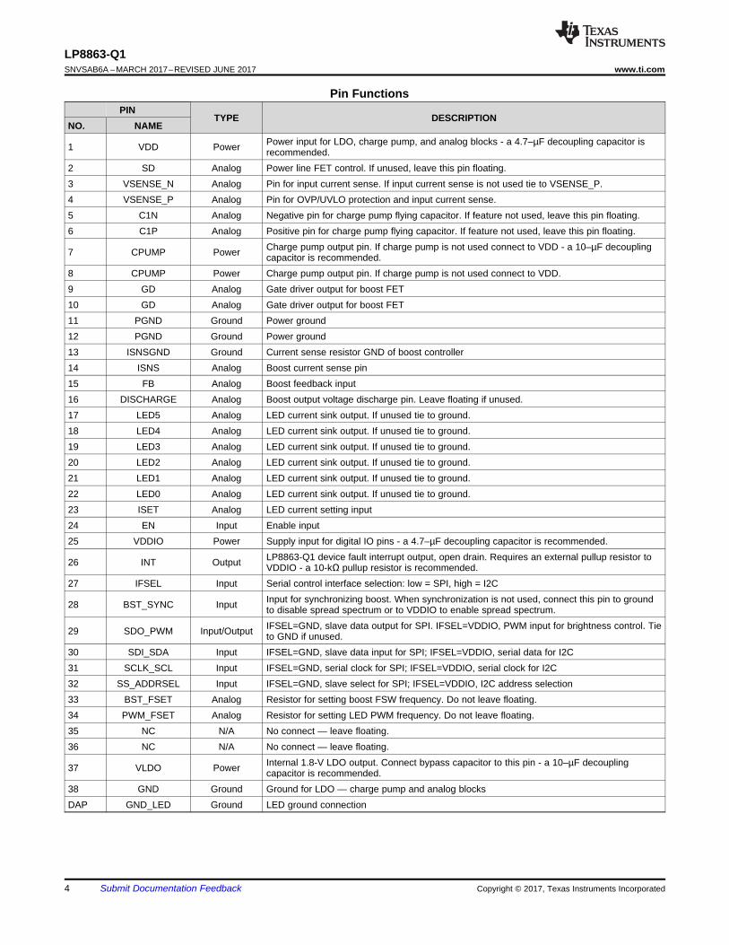
Pin FunctionsPIN
TYPE DESCRIPTIONNO. NAME
1 VDD Power Power input for LDO, charge pump, and analog blocks - a 4.7–µF decoupling capacitor isrecommended.
2 SD Analog Power line FET control. If unused, leave this pin floating.3 VSENSE_N Analog Pin for input current sense. If input current sense is not used tie to VSENSE_P.4 VSENSE_P Analog Pin for OVP/UVLO protection and input current sense.5 C1N Analog Negative pin for charge pump flying capacitor. If feature not used, leave this pin floating.6 C1P Analog Positive pin for charge pump flying capacitor. If feature not used, leave this pin floating.
7 CPUMP Power Charge pump output pin. If charge pump is not used connect to VDD - a 10–µF decouplingcapacitor is recommended.
8 CPUMP Power Charge pump output pin. If charge pump is not used connect to VDD.9 GD Analog Gate driver output for boost FET10 GD Analog Gate driver output for boost FET11 PGND Ground Power ground12 PGND Ground Power ground13 ISNSGND Ground Current sense resistor GND of boost controller14 ISNS Analog Boost current sense pin15 FB Analog Boost feedback input16 DISCHARGE Analog Boost output voltage discharge pin. Leave floating if unused.17 LED5 Analog LED current sink output. If unused tie to ground.18 LED4 Analog LED current sink output. If unused tie to ground.19 LED3 Analog LED current sink output. If unused tie to ground.20 LED2 Analog LED current sink output. If unused tie to ground.21 LED1 Analog LED current sink output. If unused tie to ground.22 LED0 Analog LED current sink output. If unused tie to ground.23 ISET Analog LED current setting input24 EN Input Enable input25 VDDIO Power Supply input for digital IO pins - a 4.7–µF decoupling capacitor is recommended.
26 INT Output LP8863-Q1 device fault interrupt output, open drain. Requires an external pullup resistor toVDDIO - a 10-kΩ pullup resistor is recommended.
27 IFSEL Input Serial control interface selection: low = SPI, high = I2C
28 BST_SYNC Input Input for synchronizing boost. When synchronization is not used, connect this pin to groundto disable spread spectrum or to VDDIO to enable spread spectrum.
29 SDO_PWM Input/Output IFSEL=GND, slave data output for SPI. IFSEL=VDDIO, PWM input for brightness control. Tieto GND if unused.
30 SDI_SDA Input IFSEL=GND, slave data input for SPI; IFSEL=VDDIO, serial data for I2C31 SCLK_SCL Input IFSEL=GND, serial clock for SPI; IFSEL=VDDIO, serial clock for I2C32 SS_ADDRSEL Input IFSEL=GND, slave select for SPI; IFSEL=VDDIO, I2C address selection33 BST_FSET Analog Resistor for setting boost FSW frequency. Do not leave floating.34 PWM_FSET Analog Resistor for setting LED PWM frequency. Do not leave floating.35 NC N/A No connect — leave floating.36 NC N/A No connect — leave floating.
37 VLDO Power Internal 1.8-V LDO output. Connect bypass capacitor to this pin - a 10–µF decouplingcapacitor is recommended.
38 GND Ground Ground for LDO — charge pump and analog blocksDAP GND_LED Ground LED ground connection

5
LP8863-Q1www.ti.com SNVSAB6A –MARCH 2017–REVISED JUNE 2017
Submit Documentation FeedbackCopyright © 2017, Texas Instruments Incorporated
(1) Stresses beyond those listed under Absolute Maximum Ratings may cause permanent damage to the device. These are stress ratingsonly, which do not imply functional operation of the device at these or any other conditions beyond those indicated under RecommendedOperating Conditions. Exposure to absolute-maximum-rated conditions for extended periods may affect device reliability.
7 Specifications
7.1 Absolute Maximum Ratingsover operating free-air temperature range (unless otherwise noted) (1)
MIN MAX UNIT
Voltage on pinsV_SENSE_P, VSENSE_N, SD, LED0 to LED5, FB, DISCHARGE –0.3 50
VVDD, EN, ISNS –0.3 5.5
Voltage on pins VDDIO, SCLK_SCL, SDI_SDA, SDO_PWM, SS_ADDRSEL, INT, IFSEL,BST_FSET, PWM_FSET, ISET –0.3 3.6 V
Voltage on pins C1P, C1N, CPUMP, GD –0.3 12 VVoltage on pins VLDO –0.3 2 V
Thermal
Continuous power dissipation Internally limitedAmbient temperature –40 125 °CJunction temperature –40 150 °CMaximum lead temperature (soldering) 260 °CStorage temperature, Tstg –65 150 °C
(1) AEC Q100-002 indicates that HBM stressing shall be in accordance with the ANSI/ESDA/JEDEC JS-001 specification.
7.2 ESD RatingsVALUE UNIT
V(ESD)Electrostaticdischarge
Human body model (HBM), per AEC Q100-002, (1) ±2000V
Charged-device model (CDM), per AEC Q100-011All pins ±500Corner pins ±750
7.3 Recommended Operating Conditionsover operating free-air temperature range (unless otherwise noted). All voltages are with respect to the potential at the GNDpins.
MIN NOM MAX UNIT
Voltage on pinsV_SENSE_P, VSENSE_N, SD 3 12 48 VLED0 to LED5, FB, DISCHARGE 0 48 V
Voltage on pins EN, ISNS 0 5.5 VVoltage on pins VDD 2.7 3.3/5 5.5 V
Voltage on pins VDDIO, SCLK_SCL, SDI_SDA, SDO_PWM, SS_ADDRSEL,INT, IFSEL, BST_FSET, PWM_FSET, ISET 1.65 1.8/3.3 3.6 V
Voltage on pinsVLDO 0 1.8 2 VC1P, C1N, CPUMP, GD 0 6.6/10 11 V
Thermal Ambient temperature –40 125 °C

6
LP8863-Q1SNVSAB6A –MARCH 2017–REVISED JUNE 2017 www.ti.com
Submit Documentation Feedback Copyright © 2017, Texas Instruments Incorporated
(1) For more information about traditional and new thermal metrics, see the Semiconductor and IC Package Thermal Metrics applicationreport.
7.4 Thermal Information
THERMAL METRIC (1)LP8863-Q1
UNITDSP (HTSSOP)38 PINS
RθJA Junction-to-ambient thermal resistance 32.4 °C/WRθJC(top) Junction-to-case (top) thermal resistance 19.5 °C/WRθJB Junction-to-board thermal resistance 8.8 °C/WψJT Junction-to-top characterization parameter 0.3 °C/WψJB Junction-to-board characterization parameter 8.9 °C/WRθJC(bot) Junction-to-case (bottom) thermal resistance 2.7 °C/W
(1) Ensured by design.
7.5 Electrical CharacteristicsLimits apply over the full operating ambient temperature range –40°C ≤ TA ≤ +125°C; unless otherwise specified, VDD = 3.3 V,VIN = 12 V, VDDIO = 1.8 V.
PARAMETER TEST CONDITIONS MIN TYP MAX UNIT
IQ
Shutdown mode current, VDD pin VDD < VPOR, EN = L 0.3 2 μAStandby mode current, VDD pin VDD > VPOR, EN = L 75 300 μA
Active mode current, VDD pin
LP8863-Q1 enabled, boost enabled(ILED = 150mA), CP enabled, VDD =3.3V, fSW = 300kHz, Boost FET -IPD25N06S4L-30
15 40 (1) mA
ƒosc Internal oscillator frequency 18.6 20 21.4 MHzVPOR Power-on reset threshold VDD pin voltage. 2.65 V
7.6 Protection Electrical CharacteristicsLimits apply over the full operating ambient temperature range –40°C ≤ TA ≤ +125°C; unless otherwise specified, VDD = 3.3 V,VIN = 12 V, VDDIO = 1.8 V.
PARAMETER TEST CONDITIONS MIN TYP MAX UNITVDDUVLO VDD UVLO threshold VDD falling 2.6 2.7 2.8 VVDDUVLO_H VDD UVLO hysteresis 0.1 VVINUVLO VIN UVLO threshold VIN falling 2.7 2.8 2.9 VVINUVLO_H VIN UVLO hysteresis 0.35 VVINOVP VIN OVP threshold VIN rising 40.8 43 45.2 VVINOVP _H VIN OVP hysteresis 2.5 VTTSD Thermal shutdown threshold Temperature rising 155 165 175 °C
TTSD_H Thermal shutdown hysteresis Temperature falling from TSDthreshold 20 °C
TTWR_H Thermal high warning threshold temperature_limit_high = 0x07D 115 125 135 °CTTWR_L Thermal low warning threshold temperature_limit_low = 0x069 95 105 115 °CVDDIO VDDIO supply voltage 1.65 3.6 VVDDIOIQ VDDIO supply current 1 μAVLDO LDO output voltage 1.8 V
7
LP8863-Q1www.ti.com SNVSAB6A –MARCH 2017–REVISED JUNE 2017
Submit Documentation FeedbackCopyright © 2017, Texas Instruments Incorporated
(1) Output Current Accuracy is the difference between the actual value of the output current and programmed value of this current.Matching is the maximum difference from the average. For the constant current sinks on the part (LED0 to LED5), the following aredetermined: the maximum output current (MAX), the minimum output current (MIN), and the average output current of all outputs (AVG).Matching number is calculated: (MAX-MIN)/AVG. The typical specification provided is the most likely norm of the matching figure for allparts. LED current sinks were characterized with 1 V headroom voltage. Note that some manufacturers have different definitions in use.
(2) Saturation voltage is defined as the voltage when the LED current has dropped 10% from the value measured at 1 V.
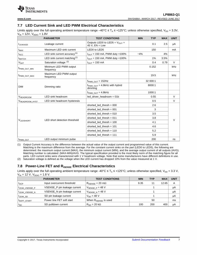
7.7 LED Current Sink and LED PWM Electrical CharacteristicsLimits apply over the full operating ambient temperature range –40°C ≤ TA ≤ +125°C; unless otherwise specified, VDD = 3.3V,VIN = 12V, VDDIO = 1.8V
PARAMETER TEST CONDITIONS MIN TYP MAX UNIT
ILEAKAGE Leakage current Outputs LED0 to LED5 = VOUT =45 V, EN = Low 0.1 2.5 µA
IMAX Maximum LED sink current LED0 to LED5 150 mAIACC LED sink current accuracy (1) IOUT = 150 mA, PWM duty =100% −4% 4%IMATCH LED sink current matching (1) IOUT = 150 mA, PWM duty =100% 1% 3.5%VSAT Saturation voltage (2) IOUT = 150 mA 0.4 0.79 V
fPWM_OUT_MINMinimum LED PWM outputfrequency
0.152 kHz
fPWM_OUT_MAXMaximum LED PWM outputfrequency 19.5 kHz
DIM Dimming ratio
fPWM_OUT = 152Hz 32 000:1fPWM_OUT = 4.8kHz with hybriddimming
8000:1
fPWM_OUT = 4.8kHz 1000:1VHEADROOM LED sink headroom led_driver_headroom = 01b 0.55 VVHEADROOM_HYST LED sink headroom hysteresis 0.5 V
VLEDSHORT LED short detection threshold
shorted_led_thresh = 000 2.6
V
shorted_led_thresh = 001 3shorted_led_thresh = 010 3.5shorted_led_thresh = 011 3.8shorted_led_thresh = 100 4.1shorted_led_thresh = 101 4.6shorted_led_thresh = 110 5.2shorted_led_thresh = 111 5.9
tPWM_OUT LED output minimum pulse 200 ns
7.8 Power-Line FET and RISENSE Electrical CharacteristicsLimits apply over the full operating ambient temperature range -40°C ≤ TA ≤ +125°C; unless otherwise specified, VDD = 3.3 V,VIN = 12 V, VDDIO = 1.8 V.
PARAMETER TEST CONDITIONS MIN TYP MAX UNITIOCP Input overcurrent threshold RISENSE = 20 mΩ 9.35 11 12.65 AILEAK_VSENSE_P VSENSE_P pin leakage current VSENSE_P = 48 V 1 µAILEAK_VSENSE_N VSENSE_N pin leakage current VSENSE_N = 48 V 1 µAILEAK_SD SD pin leakage current VSD = 48 V 1 µAtSOFT_START Power line FET soft start When RISENSE is used 50 msISD SD pulldown current RSD = 20 kΩ 100 200 400 µA

8
LP8863-Q1SNVSAB6A –MARCH 2017–REVISED JUNE 2017 www.ti.com
Submit Documentation Feedback Copyright © 2017, Texas Instruments Incorporated
7.9 Input PWM Electrical CharacteristicsLimits apply over the full operating ambient temperature range –40°C ≤ TA ≤ +125°C; unless otherwise specified, VDD = 3.3 V,VIN = 12 V, VDDIO = 1.8 V.
PARAMETER TEST CONDITIONS MIN TYP MAX UNITƒPWM_IN PWM input frequency 100 20 000 HztPWM_MIN_ON PWM input minimum on time 200 ns
INPWMRESPWM input resolution fPWM_IN = 100 Hz 16
bitfPWM_IN = 20 kHz 10
(1) Ensured by design.
7.10 Boost Converter Electrical CharacteristicsLimits apply over the full operating ambient temperature range –40°C ≤ TA ≤ +125°C; unless otherwise specified, VDD = 3.3 V,VIN = 12 V, VDDIO = 1.8 V.
PARAMETER TEST CONDITIONS MIN TYP MAX UNITVIN Input voltage 3 48 V
VOUT Output voltage
Boost mode (RFBTOP = 910 kΩ, RFBBOT =100 kΩ) 20 47
VSEPIC mode (RFBTOP = 560 kΩ, RFBBOT =170 kΩ) 6 24
ƒSW Switching frequency
BST_FSET = 3.93 kΩ 303
kHz
BST_FSET = 4.75 kΩ 400BST_FSET = 5.76 kΩ 606BST_FSET = 7.87 kΩ 800BST_FSET = 11 kΩ 1000BST_FSET = 17.8 kΩ 1250BST_FSET = 42.2 kΩ 1667BST_FSET = 140 kΩ 2200
VOUT/VIN Maximum conversion ratioBoost mode, IOUT = 6 × 150 mA 5.5 (1)
Boost mode, IOUT = 6 × 85 mA 10 (1)
SEPIC mode 0.2 5 (1)
IMAX Boost switching current limit RSENSE = 20 mΩ 9 10 11 A
VGD External FET gate drive voltageVDD = 5 V ±10%, CP Disabled 4.5 5 5.5
VVDD = 3.3 V ±10%, CP Enabled 6 6.6 7.2VDD = 5 V ±10%, CP Enabled 9 10 11
GDRDSONHRDSON of internal high side FET todrive gate of external FET
Source, VGD/(GDRDSON + total resistanceto gate input of SW FET) must not behigher than 2.5 A
1.4 Ω
GDRDSONLRDSON of internal low side FET todrive gate of external FET
Sink, VGD/(GDRDSON + total resistance togate input of SW FET) must not be higherthan 2.5 A
0.75 Ω
tSTART-UP Start-up time Delay from beginning of boost soft start towhen LED drivers can begin 50 ms
TON Minimum switch on time 120 nsTOFF Minimum switch off time 70 ns
VBST_OVPLBOOST_OVP low threshold at FBpin 1.423 V
VBST_OVPHBOOST_OVP high threshold at FBpin 1.76 V

9
LP8863-Q1www.ti.com SNVSAB6A –MARCH 2017–REVISED JUNE 2017
Submit Documentation FeedbackCopyright © 2017, Texas Instruments Incorporated
7.11 OscillatorLimits apply over the full operating ambient temperature range –40°C ≤ TA ≤ +125°C; unless otherwise specified, VDD = 3.3 V,VIN = 12 V, VDDIO = 1.8 V.
PARAMETER TEST CONDITIONS MIN TYP MAX UNITƒOSC Oscillator frequency 18.8 20 21.2 MHz
7.12 Charge PumpLimits apply over the full operating ambient temperature range –40°C ≤ TA ≤ +125°C; unless otherwise specified, VDD = 3.3 V,VIN = 12 , VDDIO = 1.8 V.
PARAMETER TEST CONDITIONS MIN TYP MAX UNITƒCP Charge pump switching frequency 387 417 447 kHz
7.13 Logic Interface CharacteristicsLimits apply over the full operating ambient temperature range –40°C ≤ TA ≤ +125°C; unless otherwise specified, VDD = 3.3 V,VIN = 12 V, VDDIO = 1.8 V.
PARAMETER TEST CONDITIONS MIN TYP MAX UNITLOGIC INPUT ENVENIL Input low level 0.4 VVENIH Input high level 1.2 VIENI Input current 5 30 µA
RPDENEN pin internal pull-downresistance 5 MΩ
LOGIC INPUT SCLK_SCL, SDI_SDA, SS_ADDRSEL, PWM, IF_SEL, BST_SYNC
VIL Input low level 0.2 ×VDDIO V
VIH Input high level 0.8 ×VDDIO V
II Input current 5 µALOGIC OUTPUT SDAVSDAOL Output low level I = 3 mA 0.3 0.5 VISDALEAKAGE Output leakage current V = 5.5 V 1 μALOGIC OUTPUT INTVINTOL Output low level IOUT = 3 mA 0.3 0.5 VIINTLEAK Output leakage current 1 μA

8
1
7 6
8
3
2
5
4
1
SCL
SDA
9
7
10
10
LP8863-Q1SNVSAB6A –MARCH 2017–REVISED JUNE 2017 www.ti.com
Submit Documentation Feedback Copyright © 2017, Texas Instruments Incorporated
7.14 Timing Requirements for SPI InterfaceMIN NOM MAX UNIT
1 Cycle time 100 ns2 Enable lead time 50 ns3 Enable lag time 50 ns4 Clock low time 45 ns5 Clock high time 45 ns6 Data setup time 20 ns7 Data hold time 20 ns8 Disable time 30 ns9 Data valid 35 ns10 SS inactive time 50 nsCb Bus capacitance 5 40 pF
7.15 Timing Requirements for I2C InterfaceMIN NOM MAX UNIT
ƒSCLK Clock frequency 400 kHz1 Hold time (repeated) START condition 0.6 µs2 Clock low time 1.3 µs3 Clock high time 600 ns4 Set-up time for a repeated START condition 600 ns5 Data hold time 50 ns6 Data setup time 100 ns7 Rise time of SDA and SCL 300 ns8 Fall time of SDA and SCL 300 ns9 Set-up time for STOP condition 600 ns10 Bus free time between a STOP and a START condition 1.3 µs
Figure 1. SPI Timing Diagram
Figure 2. I2C Timing Diagram

Brightness Code
LED
Str
ing
Cur
rent
(m
A)
0 8192 16384 24576 32768 40960 49152 57344 655360
30
60
90
120
150
D005
15 mA25 mA50 mA80 mA120 mA150 mA
Brightness Code
Cur
rent
Mat
chin
g (%
)
0 8192 16384 24576 32768 40960 49152 57344 655360.0
0.5
1.0
1.5
2.0
2.5
D006
Brightness (%)
SE
PIC
Effi
cien
cy (
%)
0 10 20 30 40 50 60 70 80 90 10055
60
65
70
75
80
85
90
D003
VIN = 6 VVIN = 12 VVIN = 17 V
Brightness (%)
SE
PIC
Effi
cien
cy (
%)
0 10 20 30 40 50 60 70 80 90 10050
55
60
65
70
75
80
85
D004
VIN = 6 VVIN = 12 VVIN = 17 V
Brightness (%)
Boo
st E
ffici
ency
(%
)
0 10 20 30 40 50 60 70 80 90 10075
80
85
90
95
100
D001
VIN = 9 VVIN = 12 VVIN = 16 VVIN = 24 V
Brightness (%)
Boo
st E
ffici
ency
(%
)
0 10 20 30 40 50 60 70 80 90 10060
65
70
75
80
85
90
95
100
D002
VIN = 9 VVIN = 12 VVIN = 16 VVIN = 24 V
11
LP8863-Q1www.ti.com SNVSAB6A –MARCH 2017–REVISED JUNE 2017
Submit Documentation FeedbackCopyright © 2017, Texas Instruments Incorporated
7.16 Typical CharacteristicsUnless otherwise specified: CIN = COUT = 2 × 10-μF ceramic and 2 × 33-μF electrolytic, VDD = 3.3 V, charge pump enabled,TA = 25°C
ƒSW = 303 kHz 8 LEDs/string 150 mA/stringL1 = 22 µH 6 strings
Figure 3. Boost Efficiency
ƒSW = 2.2 MHz 8 LEDs/string 150 mA/stringL1 = 10 µH 6 strings
Figure 4. Boost Efficiency
ƒSW = 303 kHz 2 LEDs/string 150 mA/stringL1 = 10 µH, L2 = 15 µH 6 strings
Figure 5. SEPIC Efficiency
ƒSW = 2.2 MHz 2 LEDs/string 150 mA/stringL1 = L2 = 4.7 µH 6 strings
Figure 6. SEPIC Efficiency
Figure 7. Current Linearity Figure 8. Current Matching

12
LP8863-Q1SNVSAB6A –MARCH 2017–REVISED JUNE 2017 www.ti.com
Submit Documentation Feedback Copyright © 2017, Texas Instruments Incorporated
8 Detailed Description
8.1 OverviewThe LP8863-Q1 device is a high-voltage LED driver for automotive infotainment, clusters, and other automotivedisplay LED backlight applications. It supports conventional LED backlight applications and cluster-modeapplications requiring independent duty and current control of each channel.
The LP8863-Q1 device uses the PWM input for brightness control by default. Alternatively, the brightness canalso be controlled by I2C or SPI. When two LP8863-Q1 devices are used in the system, individual I2C addressescan be selected independently with the SS_ADDRSEL pin. In cluster-mode applications each of the six LEDbrightness levels can be individually controlled via the I2C or SPI interface.
The boost frequency, LED PWM frequency, and LED string current are configured with external resistors throughthe BST_FSET, PWM_FSET, and ISET pins. The INT pin is used to report faults to the system. Fault interruptstatus can be cleared with the I2C, SPI interface, or is cleared on the falling edge of the EN pin.
The LP8863-Q1 supports pure PWM dimming and hybrid dimming; that is, combined PWM and currentbrightness control. By default PWM dimming mode is enabled, but can be changed using the I2C or SPIinterface.
The six LED current drivers provide up to 150 mA per output and can be tied together to support higher currentLEDs. The maximum output current of the LED drivers is set with the ISET resistor and can be optionally scaledby the LEDx_CURRENT[11:0] register bits with I2C or SPI interfaces. The LED output PWM frequency is set witha PWM_FSET resistor. The number of connected LED strings is automatically detected, and the deviceautomatically selects the correct phase shift. For example, if four strings are connected, the LED outputs arephase shifted by 90 degrees (= 360 / 4); if 6 strings are connected, the LED outputs are phase shifted by 60degrees (= 360 / 6). Outputs that are not used must be connected to GND. Unused outputs are disabled andexcluded from adaptive voltage and do not generate open/short LED faults. When I2C is available, LED outputscan be re-configured in cluster mode to support up to 6 individually controlled channels or, alternatively, 3 to 5channels for a display and 3 to 1 individual channels for indicator lights. In this mode all strings can be connectedto the boost of LP8863-Q1 or an external boost can be used for indicator channels.
A resistor divider connected from VOUT to the FB pin sets the maximum voltage of the boost. For best efficiencythe boost voltage is adapted automatically to the minimum necessary level needed to drive the LED strings bymonitoring all the LED output voltage drops in real time. The switching frequency of the boost regulator can beset between 300 kHz and 2.2 MHz by the BST_FSET resistor. The boost has a start-up feature that reduces thepeak current from the power-line during start-up. The LP8863-Q1 also can control a power-line FET to reducebattery leakage when disabled and provide isolation and protection in the event of a fault.
Fault detection features of LP8863-Q1 include:• Open-string and shorted LED detection
– LED fault detection prevents system overheating in case of open or short in some of the LED strings• Boost overcurrent• Boost overvoltage• Device undervoltage protection
– Threshold sensing from VDD pin• VIN input overvoltage protection (OVP)
– Threshold sensing from VSENSE_P pin• VIN input undervoltage protection
– Threshold sensing from VSENSE_P pin• VIN input overcurrent protection (OCP)
– Threshold sensing across RISENSE resistor• Thermal shutdown in case of die overtemperature• Die temperature read-out and programmable thermal window detector
LDOVLDO
Analog
Digital
Charge Pump
C1P
C1N
CPUMP
Boost Controller
GD
ISNS
ISNSGND
FB
Powerline FETControl
+-
OSC 20 MHz
LED Current Setting
PWM_FSET
BST_FSET
Digital Blocks(FSM, Adaptive Voltage Control, Fault Logic, etc.)
EN
INT
VDDIO
BST_SYNC
SDO_PWM
SDI_SDA
SCLK_SCL
SS_ADDRSEL
IFS
EL
MU
X
SPI / I2C
EEPROM
ADC TEMP Sensor
Analog Blocks (VREF, TSD, etc.)
6 x LEDCurrentSinks
LED0
LED1
LED2
LED3
LED4
LED5
VSENSE_P VSENSE_N SD
ADC
GD
PGND
PGND
ISET
Discharge DISCHARGE
IFSEL
CPUMP
GND
Copyright © 2017, Texas Instruments Incorporated
VDD
13
LP8863-Q1www.ti.com SNVSAB6A –MARCH 2017–REVISED JUNE 2017
Submit Documentation FeedbackCopyright © 2017, Texas Instruments Incorporated
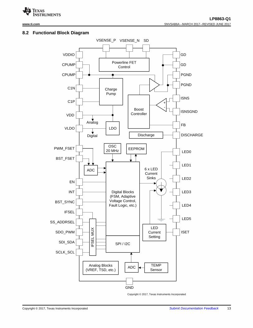
8.2 Functional Block Diagram

14
LP8863-Q1SNVSAB6A –MARCH 2017–REVISED JUNE 2017 www.ti.com
Submit Documentation Feedback Copyright © 2017, Texas Instruments Incorporated
8.3 Feature Description
8.3.1 Control InterfaceDevice control interface includes:• EN is the enable input for the LP8863-Q1 device.• INT is an open-drain fault output (indicating fault condition detection or thermal threshold crossing).• IFSEL is used for selecting between I2C and SPI.
– SPI is a 4-wire interface using SCL, SDI, SDO, and SS pins.– When SPI is selected the brightness must be controlled using the DISP_BRT and BRT_MODE registers.– I2C is a 2-wire interface using SCL and SDA pins.– When I2C is selected, the ADDRSEL pin is used to select between two alternate slave addresses.– When I2C is selected, the BRT_MODE register setting is used to select whether the brightness is
controlled by the DISP_BRT register or PWM input pin. The PWM pin is selected by default so that an I2Cinterface is not required.
• BST_SYNC is used to input an external clock for the boost switching frequency and control the internal boostclock mode.– The external clock is auto detected at start-up and, if missing, the internal clock is used.– Optionally, the BST_SYNC can be tied to VDDIO to enable the boost spread spectrum function or tied to
GND to disable it.• ISET pin to set the maximum LED current level per string.• BST_FSET pin to set the boost switching frequency.• PWM_FSET pin to set the LED output PWM dimming frequency.
Control interface is selected with IF_SEL pin according to Table 1.
Table 1. Control Interface Selection, SPI or I2CIF_SEL SERIAL INTERFACE
VDDIO (1) I2CGND (0) SPI
In I2C mode the ADDRSEL is used to select between two unique slave addresses, and the PWM input may beused to control the brightness.
8.3.2 Boost ControllerThe LP8863-Q1 current-mode-controlled boost DC-DC controller generates the bias voltage for the LEDs. Theboost is a current-mode-controlled topology with an 8-A cycle by cycle current limit. The boost converter sensesthe switch current and across the external sense resistor connected between ISNS and ISNSGND. A 25-mΩsense resistor results in an 8-A cycle by cycle current limit.. Maximum boost voltage is configured with externalFB-pin resistor divider connected between VOUT and FB. The FB-divider equation is described in Boost AdaptiveVoltage Control.

RISENSE
Q1
COUT
L1D1
CIN
VINVBOOST
S
RR R R
LIGHTLOAD
OCP
OVP
-
+
GM
GATEDRIVER
GD
FB
ADAPTIVEVOLTAGECONTROL
BOOST OSCILLATOR
MUX
OFF/BLANK TIMEPULSE GENERATOR
CURRENT RAMPGENERATOR
GM
ISNS
ISNS_GNDGBST_SYNC
BST_FSET
ADC
PGND
CPUMP
RFB1
RFB2
RBST_FSET
Copyright © 2017, Texas Instruments Incorporated
15
LP8863-Q1www.ti.com SNVSAB6A –MARCH 2017–REVISED JUNE 2017
Submit Documentation FeedbackCopyright © 2017, Texas Instruments Incorporated
Figure 9. Boost Controller Block Diagram
The boost switching frequency is adjustable from 300 kHz to 2.2 MHz via an external resistor at BST_FSET (seeTable 2).
Table 2. Boost Frequency SelectionR_BST_FSET (kΩ) BOOST FREQUENCY (kHz)
3.92 3034.75 4005.76 6067.87 80011 1000
17.8 125042.2 1667140 2200
8.3.2.1 Boost Adaptive Voltage ControlThe LP8863-Q1 boost DC-DC converter generates the bias voltage for the LEDs. During normal operation, boostoutput voltage is adjusted automatically based on the LED current sink headroom voltages. This is calledadaptive boost control. The number of used LED outputs is auto detected and only the active LED outputs aremonitored to control the adaptive boost voltage. Any LED strings with open or short faults are also removed fromthe adaptive voltage control loop. The LED driver pin voltages are periodically monitored by the control loop andthe boost voltage is raised if any of the LED outputs falls below the low headroom threshold. The boost voltage islowered if all the LED outputs are above the high headroom threshold. See Figure 10 for how the low and highheadroom thresholds automatically scale based on the LED string current and VSAT level being used.

LED
0
LED
1
LED
5
LED
0
LED
1
LED
5
LED
0
LED
1
LED
5
LED
0
LED
1
LED
5
LED0-5 PINVOLTAGE
SHORTED_LED_THRESHOLD
LED_DRV_HEADROOM
+0.5v
LED_DRV_HEADROOM
Adaptive Controlmakes no change
Adaptive Controlsteps voltage down
Adaptive Controlsteps voltage up
Adaptive Controlmakes no change
All LED0-5 outputs above threshold
One output (LED5) below threshold
Only one output (LED0) above threshold
16
LP8863-Q1SNVSAB6A –MARCH 2017–REVISED JUNE 2017 www.ti.com
Submit Documentation Feedback Copyright © 2017, Texas Instruments Incorporated
Figure 10. Adaptive Boost Voltage Control Loop Function
The external resistive divider (RFB1, RFB2) defines both the minimum and maximum adaptive boost voltage levels.The FB circuit operates the same in boost and SEPIC topologies. Choose maximum boost voltage based on themaximum LED string voltage specification. Before the LED drivers are active the boost starts up to the initialboost level. The initial boost voltage is approximately 88% of maximum boost voltage. Once the LED driverchannels are active, the boost output voltage is adjusted automatically based on LED current sink headroomvoltage. The FB pin resistor divider also scales the boost OVP and undervoltage levels.

BGMAXBOOST SEL_MAX FB1 BG
FB2
VV = (( ) + I )) R + V
Ru
+
-
GD
ISN
S
ISN
SG
ND
-
+
+
-
FB
BSTOVPL
BSTOCP
COMP
VBG ISEL[10:0]
VIN VBOOST
RFB1
RFB2
+
-BSTOVPH
-+ VUVP
VOVPL
VOVPH
17
LP8863-Q1www.ti.com SNVSAB6A –MARCH 2017–REVISED JUNE 2017
Submit Documentation FeedbackCopyright © 2017, Texas Instruments Incorporated
8.3.2.1.1 FB Divider Using Two-Resistor Method
A typical FB-pin circuit uses a two-resistor divider circuit between the boost output voltage and ground.
Figure 11. Two-Resistor FB Divider Circuit
Maximum boost voltage can be calculated with Equation 1. The maximum boost voltage can be reached duringOPEN string detection or if all LED strings are left disconnected.
where• VBG= 1.2 V• ISEL_MAX = 38.7 µA• RFB2 recommended value is 100 kΩ for boost operation and 170 kΩ for SEPIC operation. (1)
UVPBOOST _UVP SEL_MAX FB1 UVP
FB2
VV = (( ) + I ) R + V
Ru
OVPHBOOST _ OVP _HIGH SEL_MAX FB1 OVPH
FB2
VV = (( ) + I ) R + V
Ru
OVPLBOOST _ OVP _LOW SEL_MAX FB1 OVPL
FB2
VV = (( ) + I ) R + V
Ru
BGMINBOOST FB1 BG
FB2
VV = ( ) R + V
Ru
5
10
15
20
25
30
35
40
45
50
100 150 200 250 300 350 400 450 500 550 600 650 700 750 800 850 900 950
Ma
xim
um
Bo
ost
Ou
tpu
t V
olt
ag
e (
V)
R_FB1 (kOhm)
18
LP8863-Q1SNVSAB6A –MARCH 2017–REVISED JUNE 2017 www.ti.com
Submit Documentation Feedback Copyright © 2017, Texas Instruments Incorporated
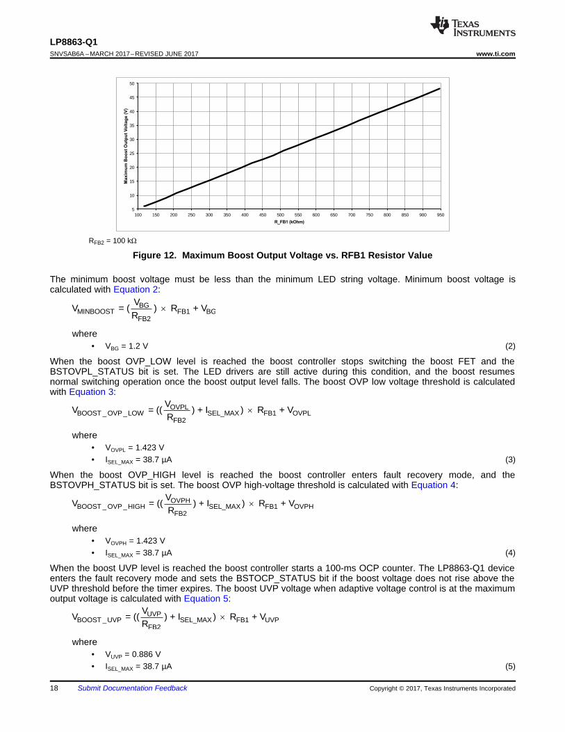
RFB2 = 100 kΩ
Figure 12. Maximum Boost Output Voltage vs. RFB1 Resistor Value
The minimum boost voltage must be less than the minimum LED string voltage. Minimum boost voltage iscalculated with Equation 2:
where• VBG = 1.2 V (2)
When the boost OVP_LOW level is reached the boost controller stops switching the boost FET and theBSTOVPL_STATUS bit is set. The LED drivers are still active during this condition, and the boost resumesnormal switching operation once the boost output level falls. The boost OVP low voltage threshold is calculatedwith Equation 3:
where• VOVPL = 1.423 V• ISEL_MAX = 38.7 µA (3)
When the boost OVP_HIGH level is reached the boost controller enters fault recovery mode, and theBSTOVPH_STATUS bit is set. The boost OVP high-voltage threshold is calculated with Equation 4:
where• VOVPH = 1.423 V• ISEL_MAX = 38.7 µA (4)
When the boost UVP level is reached the boost controller starts a 100-ms OCP counter. The LP8863-Q1 deviceenters the fault recovery mode and sets the BSTOCP_STATUS bit if the boost voltage does not rise above theUVP threshold before the timer expires. The boost UVP voltage when adaptive voltage control is at the maximumoutput voltage is calculated with Equation 5:
where• VUVP = 0.886 V• ISEL_MAX = 38.7 µA (5)

FB1 MINBOOST BG BG
FB2
RV V ( ( )) V
R u
MAXBOOST SEL _MAX FB1 SEL _MSEL_MAX F AX FB3 BGFB2
B3 BGV I 1
((I R ) + V ) R I R VR
( ) ( )ª ºª ºª º
u u « »« »« »« »« »¬ ¼¬ ¼
u¼¬
u
+
-
-+
GD
ISN
S
ISN
SG
ND
-
+
+
-
FB
VUVP
VOVPL
COMP
VBG ISEL[10:0]
VIN VBOOST
RFB1
RFB2
+
- VOVPH
RFB3
BSTOVPL
BSTOCP
BSTOVPH
19
LP8863-Q1www.ti.com SNVSAB6A –MARCH 2017–REVISED JUNE 2017
Submit Documentation FeedbackCopyright © 2017, Texas Instruments Incorporated
8.3.2.1.2 FB Divider Using Three-Resistor Method
A FB-pin circuit using a three-resistor divider circuit can be used for applications where less than 200-kΩresistors are required.
Figure 13. Three-Resistor FB Divider Circuit
Maximum boost voltage can be calculated with Equation 6. The maximum boost voltage can be reached duringOPEN string detection or if all LED strings are left disconnected.
where• VBG = 1.2 V• ISEL_MAX = 38.7 µA• RFB2 recommended value is 6 kΩ for boost operation and 10 kΩ for SEPIC operation• RFB3 recommended value is 27 kΩ for boost operation and 30 kΩ for SEPIC operation (6)
The minimum boost voltage must be less than the minimum LED string voltage. Minimum boost voltage iscalculated with Equation 7:
(7)

BOOST_UVP SEL _MAX FB1 SEL _MASEL_MAX FB X FB3 UVPFB2
3 UVPV I R I R1
((I R ) + V ) ( ) ( ) VR
ª ºª ºª º u u « u »« »« »
« »« »¬ ¼¬ ¼ ¼
u
¬
BOOST _ OVP _HIGH SEL _MAX FB1 SEL _MAX FBSEL_MAX F 3 OVPHFB2
B3 OVPHV 1
((I R ) + V ) I R( ) ( I R VR
)ª ºª ºª º
u u « »« »« »«
u u»« »¬ ¼¬ ¼¬ ¼
BOOST_OVP_LOW SEL_MAX FB1 SEL_MAX FSEL_MAX FB3 B3 OVPLFB
PL2
OVV 1
((I R ) + V ) I R( ) ( I R VR
)ª ºª ºª º
u u « »« »« »«
u u»« »¬ ¼¬ ¼¬ ¼
20
LP8863-Q1SNVSAB6A –MARCH 2017–REVISED JUNE 2017 www.ti.com
Submit Documentation Feedback Copyright © 2017, Texas Instruments Incorporated
When the boost OVP_LOW level is reached the boost controller stops switching the boost FET, and theBSTOVPL_STATUS bit is set. The LED drivers are still active during this condition, and the boost resumesnormal switching operation once the boost output level falls. The boost OVP low voltage threshold is calculatedwith Equation 8:
where• VOVPL= 1.423 V• ISEL_MAX = 38.7 µA (8)
When the boost OVP_LOW level is reached the boost controller enters fault recovery mode, and theBSTOVPH_STATUS bit is set. The boost OVP high-voltage threshold is calculated with Equation 9:
where• VOVPH = 1.76 V• ISEL_MAX = 38.7 µA (9)
When the boost UVP level is reached the boost controller starts a 100-ms OCP counter. The LP8863-Q1 deviceenters the fault recovery mode and sets the BSTOCP_STATUS bit if the boost voltage does not rise above theUVP threshold before the timer expires. The boost UVP voltage is calculated with Equation 10:
where• VUVP = 0.886 V• ISEL_MAX = 38.7 µA (10)
8.3.2.2 Boost Sync and Spread SpectrumThe boost controller can be clocked by an external BST_SYNC signal. If the external synchronization clockdisappears the boost continues operation at the frequency defined by RBST_FSET resistor. If the external syncclock disappears while the SYNC pin level is low the boost continues operation without spread spectrum. If theexternal sync clock disappears, and BST_SYNC pin remains high the boost initially stops switching forapproximately 256 μs and then begins switching with spread spectrum enabled.
If using the external BST_SYNC input, the external frequency must be between 1.2 and 1.5 times higher than thefrequency defined by the RBST_SET resistor.
The boost converter has also an internal spread spectrum function that reduces EMI noise around the switchingfrequency and its harmonic frequencies. The internal spread spectrum function modulates the boost frequency±3% from the central frequency with a 1.875-kHz modulation frequency. The spread-spectrum function cannot beused when an external synchronization clock is used.
Table 3. Boost Synchronization ModeBST_SYNC PIN LEVEL BOOST CLOCK MODE
Low (GND) Spread spectrum disabledHigh (VDDIO) Spread spectrum enabled
300-kHz to 2200-kHz clock frequency Spread spectrum disabled, external synchronization mode

LP8863-Q1C1P
C1N
CPUMP GD
ISNS
ISNSGND
FB
VS
EN
SE
_P
VS
EN
SE
_N SD
Q2 L1 D1
COUT
PGND
PGND
GD
VDD
CPUMP
VIN
RISENSE
RSD CIN
Q1
RSENSE
RFB1
RFB2
CVDD
C2X
CPUMP
VDD
21
LP8863-Q1www.ti.com SNVSAB6A –MARCH 2017–REVISED JUNE 2017
Submit Documentation FeedbackCopyright © 2017, Texas Instruments Incorporated
8.3.2.3 Boost Output DischargeWhen the boost is disabled, the discharge pin typically sinks 30-mA current in order to discharge the boostoutput voltage. The boost voltage discharge time depends on output capacitance. The discharge function isenabled for a maximum of 400 ms or until the output voltage falls below 3.3 V. The discharge state is enteredwhen the EN pin goes low. If VDD falls below the power-on reset (POR) level, the LP8863-Q1 device exits thedischarge state early and immediately enters the shutdown state. If the discharge feature is unused, leave theDISCHARGE pin floating.
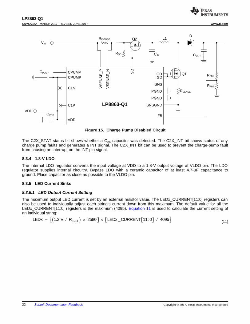
8.3.3 2X Charge PumpAn integrated 2X charge pump can be used to supply the gate drive for the external FET of the boost controller.The charge pump is enabled or disabled by automatically detecting the presence of the external C2X capacitor. IfVDD is < 4.5 V then use the charge pump to generate a high-enough gate voltage to drive the external boostswitching FET. To use the charge pump, a 2.2-µF cap is placed between C1N and C1P. If the charge pump isnot required, C1N and C1P must be left unconnected and CPUMP pins tied to VDD. A 10-µF CPUMP capacitor isused to store energy for the gate driver. The CPUMP capacitor is required to be used in both charge pumpenabled and disabled conditions and must be placed as close as possible to the CPUMP pins. Figure 14 andFigure 15 show required connections for both use cases.
Figure 14. Charge Pump Enabled Circuit
ISETILEDx 1.2 V / R 2580 LEDx _CURRENT 11: 0 / 4095ª ºº ª ª º¼ ¬ ¬ ¼u u¬ ¼
LP8863-Q1C1P
C1N
CPUMP GD
ISNS
ISNSGND
FB
VS
EN
SE
_P
VS
EN
SE
_N SD
Q2 L1D1
COUT
PGND
PGND
GD
VDD
CPUMP
VIN
RISENSE
RSD CIN
Q1
RSENSE
RFB1
RFB2
CVDD
CPUMP
VDD
22
LP8863-Q1SNVSAB6A –MARCH 2017–REVISED JUNE 2017 www.ti.com
Submit Documentation Feedback Copyright © 2017, Texas Instruments Incorporated
Figure 15. Charge Pump Disabled Circuit
The C2X_STAT status bit shows whether a C2X capacitor was detected. The C2X_INT bit shows status of anycharge pump faults and generates a INT signal. The C2X_INT bit can be used to prevent the charge-pump faultfrom causing an interrupt on the INT pin signal.
8.3.4 1.8-V LDOThe internal LDO regulator converts the input voltage at VDD to a 1.8-V output voltage at VLDO pin. The LDOregulator supplies internal circuitry. Bypass LDO with a ceramic capacitor of at least 4.7-µF capacitance toground. Place capacitor as close as possible to the VLDO pin.
8.3.5 LED Current Sinks
8.3.5.1 LED Output Current SettingThe maximum output LED current is set by an external resistor value. The LEDx_CURRENT[11:0] registers canalso be used to individually adjust each string’s current down from this maximum. The default value for all theLEDx_CURRENT[11:0] registers is the maximum (4095). Equation 11 is used to calculate the current setting ofan individual string:
(11)

LED0_DAC
LED1_DAC
LED2_DAC
LED3_DAC
LED4_DAC
LED5_DAC
LED0 Current Sink
LED0
LED1 Current Sink
LED2 Current Sink
LED3 Current Sink
LED4 Current Sink
LED5 Current Sink
LED1
LED2
LED3
LED4
LED5
ISETEXTERNAL CURRENT SETTING
RISET
LED5_CURRENT[11:0]
LED4_CURRENT[11:0]
LED3_CURRENT[11:0]
LED2_CURRENT[11:0]
LED1_CURRENT[11:0]
LED0_CURRENT[11:0]
DINDOUT
LATCH
DINDOUT
LATCH
DINDOUT
LATCH
DINDOUT
LATCH
DINDOUT
LATCH
DINDOUT
LATCH
LOAD_BRT
23
LP8863-Q1www.ti.com SNVSAB6A –MARCH 2017–REVISED JUNE 2017
Submit Documentation FeedbackCopyright © 2017, Texas Instruments Incorporated
Figure 16. LED Driver Current Setting Circuit
The LEDx_CURRENT[11:0] registers updates are also latched by the LOAD_BRT_DB register similar to theindividual brightness registers. This is done so all LED currents can be updated simultaneously. The defaultvalue for all the LEDx_CURRENT[11:0] registers is FFFh.
8.3.5.2 LED Output PWM Clock GenerationThe LED PWM frequency is asynchronous from the input PWM frequency. The LED PWM frequency isgenerated from the internal 20-MHz oscillator and can be set to eight discrete frequencies from 152 Hz to 19.531kHz. The PWM dimming resolution is highest when the lowest PWM frequency is used. The PWM_FSET resistordetermines the LED PWM frequency based on Table 4. PWM resolution in Table 4 is with PWM dither disabled.
Table 4. LED PWM Frequency SelectionR_PWM_FSET (kΩ) LED PWM FREQUENCY (Hz) PWM DIMMING RESOLUTION (bits)
3.92 152 16 (maximum)4.75 305 165.76 610 157.87 1221 1411 2441 13
17.8 4883 1242.2 9766 11140 19 531 10

24
LP8863-Q1SNVSAB6A –MARCH 2017–REVISED JUNE 2017 www.ti.com
Submit Documentation Feedback Copyright © 2017, Texas Instruments Incorporated
8.3.5.3 LED Output String ConfigurationThe six LED driver channels of the LP8863-Q1 device can automatically support applications using six, five, four,three, and two LED strings. The driver channels can also be tied together in groups of two, three, or sixchannels. This allows the LP8863-Q1 device to drive three 300-mA LED strings, two 450-mA LED strings, or one900-mA LED string. The LED strings are always appropriately phase shifted for their string configuration. Thisreduces the ripple seen at the boost output, which allows smaller output capacitors and reduces audible ringingin the capacitors. Phase shift increases the load frequency, which can move potential capacitor noise above theaudible band while still keeping PWM frequency low to support a higher dimming ratio.
When the LP8863-Q1 device is first powered on the string configuration is automatically detected and the phasesof each channel configured. The LED string configuration must not be changed unless the LP8863-Q1 ispowered off in shutdown state. The string configurations in Table 5 are valid configurations for auto detection.Any other detected configuration defaults to 6 channel / 60 degree mode. The detected string configuration canbe read from the LED_STRING_CONF[2:0] register. Tie unused LEDx pins to ground.
Table 5. LED Output String Configuration
CONFIGURATION LED0 LED1 LED2 LED3 LED4 LED5 AUTOMATICPHASE SHIFT
6 channels 150 mA 150 mA 150 mA 150 mA 150 mA 150 mA 60°5 channels 150 mA 150 mA 150 mA 150 mA 150 mA (Tied to GND) 72°4 channels 150 mA 150 mA 150 mA 150 mA (Tied to GND) (Tied to GND) 90°3 channels 150 mA 150 mA 150 mA (Tied to GND) (Tied to GND) (Tied to GND) 120°2 channels 150 mA 150 mA (Tied to GND) (Tied to GND) (Tied to GND) (Tied to GND) 180°3 channels, 300 mA/channel(tie LED pins together)
300 mA 300 mA 300 mA 120°
2 channels, 450 mA/channel(tie LED pins together)
450 mA 450 mA 180°
1 channel, 900 mA(tied LED pins together) 900 mA None
8.3.5.3.1 Independent Cluster Brightness Control Mode
The LP8863-Q1 supports a cluster mode like that found in the LP8860-Q1 LED driver. This mode allows thebrightness of each of the six driver channels to be controlled independently using the I2C or SPI interface. This isdone by using the six CLUSTER_BRTx[15:0] registers, the six LEDx_GROUP registers and theLED_EXT_SUPPLY[5:0] register.
The LEDx_GROUP registers select which CLUSTER_BRTx or DISP_BRT register is used for each of the sixLED driver channels. The LED_EXT_SUPPLY[5:0] register selects which channels are used by the adaptiveboost voltage control loop. This allows the LP8863-Q1 to drive LED strings that powered with either theintegrated boost controller or external supply. If a LED driver channel is driving a string powered from the boostthen its corresponding LED_EXT_SUPPLY bit should be set to zero. By default all LED_EXT_SUPPLY bits are0, and all LEDx_GROUP bits are 000.
An example of how the registers would be configured if the application calls for a display backlight with 4 stringsand uses the remaining 2 current sinks to drive indicator LEDs where anodes are supplied externally (not fromthe boost of the LP8863-Q1 device) follows:
LED_EXT_SUPPLY[5:0] = 11000b (LED5 and LED4 use external supply )LED0_GROUP = 000b (LED0 uses DISP_BRT register)LED1_GROUP = 000b (LED1 uses DISP_BRT register)LED2_GROUP = 000b (LED2 uses DISP_BRT register)LED3_GROUP = 000b (LED3 uses DISP_BRT register)LED4_GROUP = 100b (LED4 uses CLUSTER_BRT4 register)LED5_GROUP = 101b (LED5 uses CLUSTER_BRT5 register)

25
LP8863-Q1www.ti.com SNVSAB6A –MARCH 2017–REVISED JUNE 2017
Submit Documentation FeedbackCopyright © 2017, Texas Instruments Incorporated
8.3.6 Brightness ControlThe LP8863-Q1 supports global or individual brightness control for each LED string through individual PWM dutycycle control of the LED0 to LED5 driver channels via I2C/SPI registers. An internal 20-MHz clock is used forgenerating PWM outputs.
8.3.6.1 Brightness Control Signal PathOne display brightness path and five individual brightness paths can be used to control the LED driver channelbrightness. The LEDx_GROUP registers select whether the display brightness path or the cluster 1 to 5brightness paths control each LED output. The BRT_MODE register selects whether the input to the displaybrightness path is the PWM input pin or DISP_BRT register. The brightness control signal path diagram is shownin Figure 17.
The display brightness path has sloper and hybrid dimming functions that can be enabled. By default the sloperfunction is enabled and hybrid dimming function disabled. Both functions can be controlled using the I2C or SPIinterface. The sloper function is described in Sloper and hybrid dimming is described in Hybrid Dimming.
By default the LP8863-Q1 operates with LED0 to LED5 channels controlled by the display brightness path. Toenable individual LED string brightness control the LEDx_GROUP registers must be reconfigured with theSPI/I2C interface.
Figure 17. LP8863-Q1 Brightness Path Diagram
8.3.6.2 Hybrid DimmingIn addition to pure PWM dimming, LP8863-Q1 supports a hybrid-dimming mode. Hybrid dimming combines PWMand current modes for brightness control for the display brightness path. In hybrid mode PWM dimming is usedfor the low range of brightness, and current dimming is used for high brightness levels as shown in Figure 18.Current dimming control enables improved optical efficiency due to increased LED efficiency at lower currents.PWM dimming control at low brightness levels ensures linear and accurate control.
Hybrid mode can be enabled with the DIMMING_MODE bit in USER_CONFIG1 register. The PWM and currentmodes transition threshold can be set at 12.5% or at 0% brightness with the DIMMING_MODE bits. The latterselection allows for pure current dimming control mode.

Brightness
Brightness
Time
Time
Sloper Input
Sloper Output
Slope Time Linear Slope
Advanced Slope
26
LP8863-Q1SNVSAB6A –MARCH 2017–REVISED JUNE 2017 www.ti.com
Submit Documentation Feedback Copyright © 2017, Texas Instruments Incorporated
Figure 18. 12.5% PWM and Current Hybrid Dimming Diagram
8.3.6.3 SloperAn optional sloper function makes the transition from one brightness value to another optically smooth. By defaultthe advanced sloper is enabled with a 200-ms linear sloper duration. Transition time between two brightnessvalues is programmed with the SLOPE_SELECT[2:0] bits (when 000, sloper is disabled). With advanced sloperenabled the brightness changes are further smoothed to be more pleasing to the human eye. Advanced slope isenabled with ADV_SLOPE_ENABLE register bit.
Figure 19. Brightness Sloper

100 HzInput PWM
305 Hz LED PWMWith Minimum Pulse
Dither
300 ns = 0.003%
200 ns
3.2 ms
No Pulse
3.2 ms
200 ns
3.2 ms 3.2 ms
No Pulse
300 ns = 0.003%
Average Brightness = 0.003%
100 HzInput PWM
1.2 kHz LED PWM
Without Dither
50.003%
1.2 kHz LED PWM
With 2bit Dither
50% 50% 50% 50%
50.006% 50% 50.006% 50%
27
LP8863-Q1www.ti.com SNVSAB6A –MARCH 2017–REVISED JUNE 2017
Submit Documentation FeedbackCopyright © 2017, Texas Instruments Incorporated
8.3.6.4 DitherThe number of brightness steps when using LED output PWM dimming is equal to the 20-MHz oscillatorfrequency divided by the LED PWM frequency (set by PWM FSET resistor). The PWM duty cycle dither is afunction the LP8863-Q1 uses to increase the number of brightness dimming steps beyond this oscillator clocklimitation. The dither function modulates the LED driver output duty cycle over time to create more possibleaverage brightness levels. The DITHER_SELECT[1:0] register bits control the level of dither, disabled, 1, 2, or 3bits using the I2C or SPI interface. By default the dither is disabled.
When the 1-bit dither is selected, the width of every second PWM pulse is increased by one LSB (one 20-MHzclock period). When the 3-bit dither is selected, within a sequence of 8 PWM periods the number of pulses withincreased length varies: dither value 000 - all 8 pulses at default length; 001 - one of the 8 pulses is longer; 010 -two of the 8 pulses are longer, etc., until at 111 seven of the 8 pulses have increased length. Figure 20 showsone example of PWM output dither.
Figure 20. PWM Dither Example
The dither block also has an additional mode at low brightness levels when LED PWM duty cycle is less than theminimum pulse width (that is, less than the LED driver rise time). In this mode the dither block skips full PWMpulses to reduce the brightness further enabling very high dimming modes. The end result is the LED PWMfrequency is reduced as more and more minimum pulses are skipped or dithered out. This function can beenabled using the I2C or SPI interface by programming the EN_MIN_PWM_LIMIT bit to 1. Figure 21 shows howthe 2-bit minimum brightness dithering works.
Figure 21. Minimum Brightness Dither Example
8.3.7 Die Temperature Read-Out and Thermal Window DetectorThe LP8863-Q1 has two internal thermal sensors: one for protection purposes (device thermal shutdown) andone for die temperature monitoring. The die temperature monitor block includes a 9-bit ADC to convert theanalog thermal-sensor output to a temperature reading available in the register JUNCTION_TEMPERATURE.First temperature result is available 2 ms after the activation of the block and conversion rate is 10 Hz. When thetemperature monitor block is disabled register JUNCTION_TEMPERATURE content is –256°C.

Temperature Monitor
ADC
Thermal Sensor
Window Detector
TSD Thermal Sensor
INTInterrupts
INT
TEMPLOW_STATUS
TEMPHIGH_STATUS
TSD_STATUS
TEMPERATURE_LIMIT_LOW
TEMPERATURE_LIMIT_HIGH
JUNCTION_TEMPERATURE
TEMP_MON_EN
I2C/SPI
28
LP8863-Q1SNVSAB6A –MARCH 2017–REVISED JUNE 2017 www.ti.com
Submit Documentation Feedback Copyright © 2017, Texas Instruments Incorporated
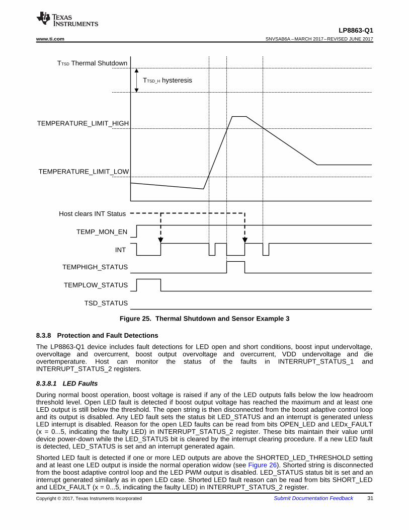
The die temperature monitor also includes a thermal window detector. The TEMPERATURE_LIMIT_HIGH andTEMPERATURE_LIMIT_LOW bits set the high and low limits for the thermal window. These thresholds have±1°C hysteresis: TEMPERATURE _LIMIT_HIGH + 1°C for increasing and TEMPERATURE_LIMIT_HIGH – 1°Cfor decreasing, for example. If the die temperature increases above the high limit or reduces below the low limit,a fault interrupt is generated. Die temperature monitor (ADC, thermal sensor, and window detector) can bedisabled to minimize power dissipation in STANDBY mode. The thermal sensor for TSD is always active.
Figure 22. Thermal Shutdown and Sensor Block Diagram
Figure 23, Figure 24, and Figure 25 show the INT pin and status behaviors of the TSD, temperature high, andtemperature low limits.

TEMPERATURE_LIMIT_LOW
TEMPERATURE_LIMIT_HIGH
TTSD Thermal Shutdown
TTSD_H hysteresis
TEMP_MON_EN
INT
TEMPLOW_STATUS
TEMPHIGH_STATUS
TSD_STATUS
Host clears INT Status
Enters Standby Mode
Returns to Normal Mode
29
LP8863-Q1www.ti.com SNVSAB6A –MARCH 2017–REVISED JUNE 2017
Submit Documentation FeedbackCopyright © 2017, Texas Instruments Incorporated
Figure 23. Thermal Shutdown and Sensor Example 1

TEMPERATURE_LIMIT_LOW
TEMPERATURE_LIMIT_HIGH
TTSD Thermal Shutdown
TTSD_H hysteresis
TEMP_MON_EN
INT
TEMPLOW_STATUS
TEMPHIGH_STATUS
TSD_STATUS
Host clears INT Status
30
LP8863-Q1SNVSAB6A –MARCH 2017–REVISED JUNE 2017 www.ti.com
Submit Documentation Feedback Copyright © 2017, Texas Instruments Incorporated
Figure 24. Thermal Shutdown and Sensor Example 2
TTSD_H hysteresis
TEMPLOW_STATUS
TEMPHIGH_STATUS
TSD_STATUS
TTSD Thermal Shutdown
TEMPERATURE_LIMIT_HIGH
TEMPERATURE_LIMIT_LOW
Host clears INT Status
TEMP_MON_EN
INT
31
LP8863-Q1www.ti.com SNVSAB6A –MARCH 2017–REVISED JUNE 2017
Submit Documentation FeedbackCopyright © 2017, Texas Instruments Incorporated
Figure 25. Thermal Shutdown and Sensor Example 3
8.3.8 Protection and Fault DetectionsThe LP8863-Q1 device includes fault detections for LED open and short conditions, boost input undervoltage,overvoltage and overcurrent, boost output overvoltage and overcurrent, VDD undervoltage and dieovertemperature. Host can monitor the status of the faults in INTERRUPT_STATUS_1 andINTERRUPT_STATUS_2 registers.
8.3.8.1 LED FaultsDuring normal boost operation, boost voltage is raised if any of the LED outputs falls below the low headroomthreshold level. Open LED fault is detected if boost output voltage has reached the maximum and at least oneLED output is still below the threshold. The open string is then disconnected from the boost adaptive control loopand its output is disabled. Any LED fault sets the status bit LED_STATUS and an interrupt is generated unlessLED interrupt is disabled. Reason for the open LED faults can be read from bits OPEN_LED and LEDx_FAULT(x = 0...5, indicating the faulty LED) in INTERRUPT_STATUS_2 register. These bits maintain their value untildevice power-down while the LED_STATUS bit is cleared by the interrupt clearing procedure. If a new LED faultis detected, LED_STATUS is set and an interrupt generated again.
Shorted LED fault is detected if one or more LED outputs are above the SHORTED_LED_THRESHOLD settingand at least one LED output is inside the normal operation widow (see Figure 26). Shorted string is disconnectedfrom the boost adaptive control loop and the LED PWM output is disabled. LED_STATUS status bit is set and aninterrupt generated similarly as in open LED case. Shorted LED fault reason can be read from bits SHORT_LEDand LEDx_FAULT (x = 0...5, indicating the faulty LED) in INTERRUPT_STATUS_2 register.

32
LP8863-Q1SNVSAB6A –MARCH 2017–REVISED JUNE 2017 www.ti.com
Submit Documentation Feedback Copyright © 2017, Texas Instruments Incorporated
Figure 26. LED Open and Short Detection Logic
8.3.8.2 Boost FaultsBoost overvoltage is detected if the FB pin voltage exceeds the VOVPL threshold. When boost overvoltage isdetected, BSTOVPL_STATUS bit is set in the INTERRUPT_STATUS_1 register. The boost FET stops switching,and the output voltage is automatically limited. If the BSTOVPL_STATUS bit is continually set (that is, reappearsafter clearing), it may indicate an issue in the application. Boost overvoltage low is monitored during devicenormal operation (ACTIVE mode).
A second boost overvoltage high fault is detected if the FB pin voltage exceeds the VOVPH threshold. TheLP8863-Q1 device enters the fault recovery state to protect against excessive thermal dissipation caused by highheadroom on the LED drivers. When boost overvoltage is detected, BSTOVPH_STATUS bit is set in theINTERRUPT_STATUS_1 register. A fault interrupt is also generated. If the BSTOVPH_STATUS bit is continuallyset (that is, reappears after clearing), it may indicate an issue in the application. Boost overvoltage high ismonitored during device normal operation (ACTIVE mode).
Boost overcurrent is detected if the FB pin voltage drops below the VUVP threshold. A boost OCP fault is detectedif the undervoltage condition persists for longer than 1600 milliseconds. If the boost overcurrent timer expiresbefore the output voltage recovers, the BSTOCP_STATUS bit is set in the INTERRUPT_STATUS_1 register.The fault recovery state is entered, and a fault interrupt is generated. If the BSTOCP_STATUS bit is permanentlyset, it may indicate an issue in the application. Boost overcurrent is monitored from the boost start, and fault maytrigger during boost start-up.
8.3.8.3 Power-Line FaultsIf during operation of the LP8863-Q1 device the VIN (VSENSE_P pin) voltage falls below the VINUVLO fallinglevel, the boost, LED outputs, and power-line FET are turned off, and the device enters STANDBY mode. TheVINUVLO_STATUS bit is also set, and the INT pin is triggered. When the VINUVLO voltage rises above therising threshold level the LP8863-Q1 device exits STANDBY and begins the start-up sequence.
If during LP8863-Q1 device operation VIN (VSENSE_P pin) voltage rises above the VINOVP rising level, boost,LED outputs, and power-line FET are turned off, and the device enters STANDBY mode. The VINOVP_STATUSbit is also set, and the INT pin is triggered. When the VINOVP voltage falls below the falling threshold level theLP8863-Q1 exits STANDBY and begins the start-up sequence.
The VIN OCP protection detects overcurrent by measuring voltage of the RISENSE resistor connected betweenVSENSE_P and VSENSE_N pins. VIN OCP sensing begins once the LP8863-Q1 enters the PL FET soft-startstate. Fault is detected if undervoltage condition duration lasts for at least 10 μs, minimum. TheVINOCP_STATUS bit is also set, and the INT pin is triggered. To trip at a lower current limit a larger senseresistor can be used to create a 220-mV voltage difference across the sense resistor.

33
LP8863-Q1www.ti.com SNVSAB6A –MARCH 2017–REVISED JUNE 2017
Submit Documentation FeedbackCopyright © 2017, Texas Instruments Incorporated
8.3.8.4 VDD Undervoltage FaultIf during LP8863-Q1 device operation VDD falls below VDDUVLO falling level, boost, PL FET, and LED outputsare turned off, and the device enters STANDBY mode. The VDDUVLO_STATUS fault bit is set, and the INT pinis triggered. The LP8863-Q1 recovers automatically to ACTIVE mode when VDD rises above VDDUVLO risingthreshold.
If VDD falls below VPOR the LP8863-Q1 device enters SHUTDOWN mode.
8.3.8.5 Thermal ShutdownIf the die temperature of LP8863-Q1 reaches the thermal shutdown threshold TTSD, the boost, PL FET, and LEDoutputs on LP8863-Q1 device shut down to protect the device from damage. Fault status bit TSD_STATUS bit isset, and the INT pin is triggered. The device restarts the PL FET, the boost, and LED outputs when temperaturedrops by TTSD_H amount.

LP8863-Q1SNVSAB6A –MARCH 2017–REVISED JUNE 2017 www.ti.com
34 Submit Documentation Feedback Copyright © 2017, Texas Instruments Incorporated
8.3.8.6 Overview of the Fault/Protection Schemes
FAULT NAME STATUS BIT CONDITION TRIGGER FAULTINTERRUPT
ENTER FAULTRECOVERY ACTION
Boost overcurrent BSTOCP_STATUS FB pin voltages falls below VUVP levelfor > 110 ms Yes Yes Device goes to standby and then attempts to
restart 200 ms after fault occurs.
Boost overvoltage low BSTOVPLOW_STATUS FB pin voltages rises above VOVPL level No NoBoost stops switching until boost voltage levelfalls. The device remains in normal mode withLED drivers operational.
Boost OVP high BSTOVPH_STATUS FB pin voltages rises above VOVPH level Yes Yes Device goes to standby and waits until outputvoltage falls below threshold before restarting.
Boost sync clock invalid BSTSYNC_STATUS
Device is enabled while a valid externalSYNC clock is running. Then SYNCstops or changes to invalid frequency.Valid range is 1.2× to 1.5× of frequencyselected by BST_FSET resistor.
No No
Device defaults to internal clock frequencyselected by BST_FSET resistor. If SYNC input isheld high then spread spectrum is enabled. IfSYNC input is held low then spread spectrum isdisabled.
VIN overvoltage VINOVP_STATUS VIN voltage rises above 43 V. Yes No Device goes to standby and waits until outputvoltage falls below threshold before restarting.
VIN undervoltage VINUVLO_STATUS VIN voltage falls below 2.8 V. Yes NoDevice goes to standby and then attempts torestart once the input voltage rises abovethreshold.
VIN overcurrent VINOCP_STATUS Voltage across RISENSE exceeds 220mV Yes Yes Device goes to standby and then attempts to
restart 200 ms after fault occurs.
VDD undervoltage VDDUVLO_STATUS VDD level falls below VDDUVLOthreshold. Yes No Device restarts once VDD level rises above
VDDUVLO threshold.
Thermal shutdown TSD_STATUS Junction temperature rises above TTSDthreshold. Yes No Device goes to standby and then attempts to
restart once die temperature falls below threshold.
Open LED string LED_STATUSOPEN_LED
Headroom voltage on one or morechannels is below minimum level andboost has adapted to maximum level.
Yes NoFaulted LED string is disabled and removed fromadaptive boost control loop. String is re-enablednext power cycle.
Shorted LED LED_STATUS
Headroom voltage on one or morechannels is above theSHORTED_LED_THRESHOLD for > 5ms while the headroom of at least onechannel is still below this threshold.
Yes NoFaulted LED string is disabled and removed fromadaptive boost control loop. String is re-enablednext power cycle.
Invalid LED string detected INVSTRING_STATUS LED string detection does not matchone of 8 valid configurations Yes No Device defaults to six LED string phase shift
mode. String detection reoccurs next power cycle.
FSET detection fault FSET_STATUS BST_FSET or PWM_FSET are missingor an invalid value Yes No Device starts up using fail-safe values.
Charge pump fault CP_STATUS Charge pump voltage level is abnormal. No NoDevice functions normally, if possible. If chargepump issue is severe, it is likely boost overcurrentfault will trip.
Charge pump componentsmissing CPCAP_STATUS Charge pump is missing components. No No
Device functions normally, if possible. If chargepump issue is severe, it is likely boost overcurrentfault will trip.

SHUTDOWN
DEVICE INIT
STANDBY
PL FETSOFTSTART
BOOST STARTUP
NORMAL
FAULT RECOVERY
VDD > POR
From Any StateVDD < POR
EN=1
50 ms and BOOST_OK=1
50 ms and BOOST_OK=0
200 ms and PL_PRECHARGE_READY
50 ms and PL_PRECHARGE_COMPLETE
All LED channels have been disabled due to open or short faults.
LATCH FAULT
DISCHARGE_DONE andEN=0DISCHARGE
EN=0
FAULT
35
LP8863-Q1www.ti.com SNVSAB6A –MARCH 2017–REVISED JUNE 2017
Submit Documentation FeedbackCopyright © 2017, Texas Instruments Incorporated
8.4 Device Functional Modes
8.4.1 State Diagram
Figure 27. State Machine Diagram
8.4.2 ShutdownWhen VDD is below POR threshold device is in shutdown state.
8.4.3 Device InitializationAfter POR is released device initialization begins. During this state the LDO is started up, EEPROM default andtrim configurations are loaded, BOOST_FSET and PWM_FSET resistors are detected, and the LED stringconfiguration is detected.

36
LP8863-Q1SNVSAB6A –MARCH 2017–REVISED JUNE 2017 www.ti.com
Submit Documentation Feedback Copyright © 2017, Texas Instruments Incorporated
Device Functional Modes (continued)8.4.4 Standby ModeIn standby the LP8863-Q1 device can be accessed with I2C or SPI to change any configuration registers. Analogblocks are disabled to save power.
8.4.5 Power-line FET Soft StartPower-line FET is enabled, and boost input and output capacitors are charged to VIN level. VIN faults for OCP,OVP, and UVP are enabled.
8.4.6 Boost Start-UpBoost voltage is ramped to maximum voltage level with reduced current limit. Start-up exits when boost reachesinitial target voltage. All boost faults are now enabled.
8.4.7 Normal ModeLED drivers are enabled when brightness is greater than zero. All LED faults are active.
8.4.8 Discharge ModeWhen EN goes low from normal mode the boost output voltage is discharged. This state exits when boostvoltage falls below 3.3 V or when the 300-ms timer expires.
8.4.9 Fault RecoveryNon-LED faults can trigger fault recover state. LED drivers, boost converter, and power-line FET are disabled for200 ms, and the device attempts to restart from standby mode if EN is still high.
8.4.10 Latch FaultIf all LED strings are disabled due to faults then the LP8863-Q1 enters the latch fault mode. This state can beexited by toggling the EN pin.

VIN
VDD
EN
PWM Input Pin
VDDIO
SHUTDOWNDEVICE
INITSTANDBY
PL FET PRECHARGE
BOOST SOFTSTART
NORMAL
Boost VOUT
LEDx
VIN
VADAPTVINIT
STATE
50 ms 50 ms
37
LP8863-Q1www.ti.com SNVSAB6A –MARCH 2017–REVISED JUNE 2017
Submit Documentation FeedbackCopyright © 2017, Texas Instruments Incorporated
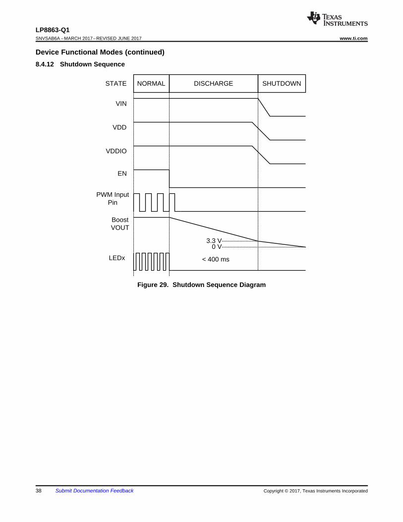
Device Functional Modes (continued)8.4.11 Start-Up Sequence
Figure 28. Start-Up Sequence Diagram
VIN
VDD
EN
PWM Input Pin
VDDIO
SHUTDOWNNORMAL
Boost VOUT
LEDx
STATE DISCHARGE
3.3 V0 V
< 400 ms
38
LP8863-Q1SNVSAB6A –MARCH 2017–REVISED JUNE 2017 www.ti.com
Submit Documentation Feedback Copyright © 2017, Texas Instruments Incorporated
Device Functional Modes (continued)8.4.12 Shutdown Sequence
Figure 29. Shutdown Sequence Diagram

39
LP8863-Q1www.ti.com SNVSAB6A –MARCH 2017–REVISED JUNE 2017
Submit Documentation FeedbackCopyright © 2017, Texas Instruments Incorporated
8.5 Programming
8.5.1 Serial Interface SelectionThe serial interface type is selected by connecting the IFSEL pin to VDDIO or GND. The LP8863-Q1 devicechecks the IFSEL pin state as part of device startup. Device start-up occurs after VDD and VDDIO POR levelsare reached. Table 6 shows how to connect the IFSEL pin to select between the SPI and I2C-compatibleinterfaces.
Table 6. Serial Control Interface SelectionPIN NAME IFSEL PIN = VDDIO IFSEL PIN = GND
SS_ADDRSEL ADDRSEL SSSCLK_SCL SCL SCLKSDI_SDA SDA SDI
SDO_PWM PWM SDO
8.5.2 SPI InterfaceIn SPI mode host can address as many unique LP8863-Q1 devices as there are slave select pins on host. Thecomplete 10-bit register space in LP8863-Q1 device can be accessed using SPI interface.
The LP8863-Q1 device is compatible with SPI serial-bus specification and operates as a slave device. Thetransmission consists of 32-bit write and read cycles. One cycle consists of a 15-bit register address (10 bitsused), 1 read/write (R/W) bit and 16-bit data to maintain compatibility with 16-bit SPI.
The R/W bit high state defines a write cycle and low defines a read cycle. The SDO output is normally in a high-impedance state. When the slave-select pin SS for the device is active (that is, low) the SDO output is pulledlow. During write cycle SDO stays in high-impedance state. The address and data bits are transmitted MSB first.The slave-select signal SS must be low during the cycle transmission. SS resets the interface when high, and ithas to be taken high between successive cycles, except when using auto- increment mode. Data is clocked in onthe rising edge of the SCLK clock signal, while data is clocked out on the falling edge of SCLK.
Figure 30. SPI Write
Figure 31. SPI Read

40
LP8863-Q1SNVSAB6A –MARCH 2017–REVISED JUNE 2017 www.ti.com
Submit Documentation Feedback Copyright © 2017, Texas Instruments Incorporated
8.5.3 I2C-Compatible InterfaceTwo LP8863-Q1 slave devices may share the same I2C bus. The SS_ADDRSEL pin selects between the twopossible base slave addresses.
Table 7. I2C Address SelectionSS_ADDRSEL PIN 7-BIT I2C BASE SLAVE ADDRESS
GND 0x2CVDDIO 0x3C
The LP8863-Q1 uses a 10-bit register address space. The 10-bit register address space is accessed as fourseparate 8-bit address spaces. Four different slave addresses are used to access each of the four 8-bit addressregister spaces.
Table 8. I2C Address Registers SelectionSS_ADDRSEL PIN 7-BIT BASE ADDRESS 7-BIT SLAVE ADDRESS ACCESSIBLE 10-BIT REGISTERS
GND 0x2C
0x2C 0x000 to 0x0FF0x2D 0x100 to 0x1FF0x2E 0x200 to 0x2FF0x2F 0x300 to 0x3FF
VDDIO 0x3C
0x3C 0x000 to 0x0FF0x3D 0x100 to 0x1FF0x3E 0x200 to 0x2FF0x3F 0x300 to 0x3FF
Write I2C transactions are made up of 4 bytes. The first byte includes the 7-bit slave address and Write bit. The7-bit slave address selects the LP8863-Q1 slave device and one of four 8-bit register address sections. Thesecond byte includes eight LSB bits of the 10-bit register address. The last two bytes are the 16-bit registervalue.
Read I2C transactions are made up of five bytes. The first byte includes the 7-bit slave address and Write bit.The 7-bit slave address selects the LP8863-Q1 slave device and one of four 8-bit register address sections. Thesecond byte includes eight LSB bits of the 10-bit register address. The third byte includes the 7-bit slave addressand Read bit. The last two bytes are the 16-bit register value returned from the slave.
Figure 32. I2C Write
Figure 33. I2C Read

41
LP8863-Q1www.ti.com SNVSAB6A –MARCH 2017–REVISED JUNE 2017
Submit Documentation FeedbackCopyright © 2017, Texas Instruments Incorporated
8.5.4 Programming Examples
8.5.4.1 General Configuration RegistersThe LP8863-Q1 does not require any serial interface configuration. It can be simply controlled with the EN pinand PWM pin. Most of the device configuration is accomplished using external resistor values or automaticdetection. If a serial interface is available then extended configuration is possible. The configuration registers canbe written in standby state as shown in Table 9.
Table 9. Configuration RegistersREGISTER NAME FUNCTION
BRT_MODE Selects PWM pin or DISPLAY_BRT register for brightness control.SHORTED_LED_THRESHOLD Selects voltage level for shorted LED Fault.DITHER_SELECT Selects up to 3 bits of PWM dither for added dimming resolution.
EN_MIN_PWM_LIMIT Enables 200-ns PWM pulse limit and frequency dither to reach lower minimum brightnesslevels.
SLOPE_SELECT Selects duration for linear brightness sloper.ADV_SLOPE_ENABLE Enables advance sloper S-shape smoothing function.DIMMING_MODE Select between PWM, hybrid or current LED ouput dimming types.TEMP_MON_EN Enables temperature window monitor function.TEMPERATURE_LIMIT_HIGH Sets HIGH threshold level for temperature window function.TEMPERATURE_LIMIT_LOW Sets LOW threshold level for temperature window function.
8.5.4.2 Clearing Fault InterruptsThe LP8863-Q1 has an INT pin to alert the host when a fault occurs. If a serial interface is available, the InterruptFault Status registers can be read back to learn which fault(s) have been detected. These status bits are locatedin the INTERRUPT_STATUS_1, INTERRUPT_STATUS_2, and INTERRUPT_STATUS_3 registers. Eachinterrupt status has a STATUS bit and a CLEAR bit. If a fault interrupt has been detected, a 1 is read back fromits STATUS bit. To clear a fault interrupt status a 1 must be written to both the STATUS bit and CLEAR bit at thesame time.
8.5.4.3 Disabling Fault InterruptsBy default most of the LP8863-Q1 faults trigger the INT pin. Each fault has two INT_EN bits. These bits arelocated in the INTERRUPT_ENABLE_1, INTERRUPT_ENABLE_2, and INTERRUPT_ENABLE_3 registers. If theINT_EN bit is read and returns a 1, the INT pin is triggered when that fault occurs. The fault interrupt can bedisabled by writing 01 to its INT_EN bits, or it can be enabled by writing 11 to its INT_EN bits. There is also aGLOBAL fault interrupt that can be disabled to prevent any faults from triggering the INT pin.
8.5.4.4 Diagnostic RegistersThe LP8863-Q1 contains several diagnostic registers than can be read with the serial interface for debugging oradditional device information. Table 10 is a summary of the available registers.
Table 10. Diagnostic RegistersREGISTER NAME FUNCTION
JUNCTION_TEMPERATURE 9-bit die junction temperature in 2s complement form — 1°C per LSBFSM_LIVE_STATUS Current state of the functional state machinePWM_INPUT_STATUS Measured 6-bit duty cycle of the PWM pin inputLED_PWM_STATUS 16-bit LED0 PWM duty cycle from state machineLED_CURRENT_STATUS 12-bit LED0 current DAC value from state machine
VBOOST_STATUS 10-bit value for adaptive boost voltage target — value is linear betweenVBOOST_MIN and VBOOST_MAX calculations
AUTO_PWM_FREQ_SEL LED PWM frequency value from PWM_FSET detectionAUTO_BOOST_FREQ_SEL Boost switching frequency value from PWM_FSET detectionAUTO_LED_STRING_CFG LED string phase configuration detected from LED pin configuration

42
LP8863-Q1SNVSAB6A –MARCH 2017–REVISED JUNE 2017 www.ti.com
Submit Documentation Feedback Copyright © 2017, Texas Instruments Incorporated
8.5.4.5 Cluster Mode Configuration and Control RegistersThe LP8863-Q1 device supports a cluster mode where the duty cycles and LED current of the six LED currentdrivers can be controlled independently. This mode can also select which LED current driver’s headroom levelsare used by the adaptive boost voltage control loop. If the anode of an LED string is supplied by an externalsupply and not the integrated boost controller then its LED_EXT_SUPPLY bit is set to 1. The cluster modeconfiguration registers are summarized in Table 11. More details can be found in Register Maps.
Table 11. Cluster Mode Configuration RegistersREGISTER NAME FUNCTION
LED0_GROUP...LED5_GROUP Selects which of the five CLUSTERx_BRT or DISPLAY_BRT registers control eachLED current driver.
CLUSTER1_BRT…CLUSTER5_BRT Five 16-bit brightness values that can be used in addition to the DISPLAY_BRTregister.
LED0_CURRENT…LED5_CURRENT Six 12-bit current registers allow LED current to be independently scaled frommaximum level for LED current driver.
LOAD_BRT_DB Load BRT bit is written to 1 in order to update the CLUSTERx_BRT andLEDx_CURRENT registers at the same time.
LED_EXT_SUPPLY Six bits to select which LED current driver is powered from an external supply and notthe boost converter.
LED0_SHORT_DISABLE…LED5_SHORT_DISABLE
Six bits to individually disable LED short detection for each LED current driver. Used ifLED current value is set to lower value than other strings.

43
LP8863-Q1www.ti.com SNVSAB6A –MARCH 2017–REVISED JUNE 2017
Submit Documentation FeedbackCopyright © 2017, Texas Instruments Incorporated
8.6 Register Maps
8.6.1 FULLMAP RegistersTable 12 lists the memory-mapped registers for the FULLMAP. All register offset addresses not listed in Table 12should be considered as reserved locations and the register contents should not be modified.
Table 12. FULLMAP RegistersOffset Acronym Register Name Section
20h BL_MODE Brightness Mode Go28h DISP_BRT Display Brightness Go30h GROUPING1 Brightness Grouping 1 Go32h GROUPING2 Brightness Grouping 2 Go40h USER_CONFIG1 User Config 1 Go42h USER_CONFIG2 User Config 2 Go4Eh INTERRUPT_ENABLE_3 Fault Interrupt Enable 3 Go50h INTERRUPT_ENABLE_1 Fault Interrupt Enable 1 Go52h INTERRUPT_ENABLE_2 Fault Interrupt Enable 2 Go54h INTERRUPT_STATUS_1 Fault Interrupt Status 1 Go56h INTERRUPT_STATUS_2 Fault Interrupt Status 2 Go58h INTERRUPT_STATUS_3 Fault Interrupt Status 3 GoE8h JUNCTION_TEMPERATURE Die Junction Temperature GoECh TEMPERATURE_LIMIT_HIGH Temperature High Limit GoEEh TEMPERATURE_LIMIT_LOW Temperature Low Limit Go13Ch CLUSTER1_BRT Cluster 1 Brightness Go148h CLUSTER2_BRT Cluster 2 Brightness Go154h CLUSTER3_BRT Cluster 3 Brightness Go160h CLUSTER4_BRT Cluster 4 Brightness Go16Ch CLUSTER5_BRT Cluster 5 Brightness Go178h BRT_DB_CONTROL Cluster Brightness and Current Load Bit Go1C2h LED0_CURRENT LED0 Current Go1C4h LED1_CURRENT LED1 Current Go1C6h LED2_CURRENT LED2 Current Go1C8h LED3_CURRENT LED3 Current Go1CAh LED4_CURRENT LED4 Current Go1CCh LED5_CURRENT LED5 Current Go288h BOOST_CONTROL Boost Control Go28Ah SHORT_THRESH Shorted LED Threshold Go2A4h FSM_DIAGNOSTICS Device State Diagnostics Go2A6h PWM_INPUT_DIAGNOSTICS PWM Input Diagnostics Go2A8h PWM_OUTPUT_DIAGNOSTICS PWM Output Diagnostics Go2AAh LED_CURR_DIAGNOSTICS LED Current Diagnostics Go2ACh ADAPT_BOOST_DIAGNOSTICS Adaptive Boost Diagnostics Go2AEh AUTO_DETECT_DIAGNOSTICS Auto Detect Diagnstics Go
Complex bit access types are encoded to fit into small table cells. Table 13 shows the codes that are used foraccess types in this section.
Table 13. FULLMAP Access Type CodesAccess Type Code DescriptionRead TypeR R Read

44
LP8863-Q1SNVSAB6A –MARCH 2017–REVISED JUNE 2017 www.ti.com
Submit Documentation Feedback Copyright © 2017, Texas Instruments Incorporated
Table 13. FULLMAP Access Type Codes (continued)Access Type Code DescriptionWrite TypeW W WriteReset or Default Value-n Value after reset or the default
value
8.6.1.1 BL_MODE Register (Offset = 20h) [reset = 300h]BL_MODE is shown in Figure 34 and described in Table 14.
Return to Summary Table.
Figure 34. BL_MODE Register
15 14 13 12 11 10 9 8RESERVED
R/W-C0h
7 6 5 4 3 2 1 0RESERVED brightness_mode
R/W-C0h R/W-0h
Table 14. BL_MODE Register Field DescriptionsBit Field Type Reset Description
15-2 RESERVED R/W C0h These bits are reserved.1-0 brightness_mode R/W 0h
0h = Brightness controlled by PWM Input1h = Reserved2h = Brightness controlled by DISPLAY_BRT Register3h = Reserved
8.6.1.2 DISP_BRT Register (Offset = 28h) [reset = 0h]DISP_BRT is shown in Figure 35 and described in Table 15.
Return to Summary Table.
Figure 35. DISP_BRT Register
15 14 13 12 11 10 9 8 7 6 5 4 3 2 1 0DISPLAY_BRT
R/W-0h
Table 15. DISP_BRT Register Field DescriptionsBit Field Type Reset Description
15-0 DISPLAY_BRT R/W 0h Display Brightness Register
8.6.1.3 GROUPING1 Register (Offset = 30h) [reset = 0h]GROUPING1 is shown in Figure 36 and described in Table 16.
Return to Summary Table.

45
LP8863-Q1www.ti.com SNVSAB6A –MARCH 2017–REVISED JUNE 2017
Submit Documentation FeedbackCopyright © 2017, Texas Instruments Incorporated
Figure 36. GROUPING1 Register
15 14 13 12 11 10 9 8LED3_GROUP LED2_GROUP
R/W-0h R/W-0h
7 6 5 4 3 2 1 0LED1_GROUP LED0_GROUP
R/W-0h R/W-0h
Table 16. GROUPING1 Register Field DescriptionsBit Field Type Reset Description
15-12 LED3_GROUP R/W 0h LED Output 3 Brightness Control Mapping0h = DISP_BRT/PWM1h = CLUSTER1_BRT2h = CLUSTER3_BRT3h = CLUSTER3_BRT4h = CLUSTER4_BRT5h = CLUSTER5_BRT
11-8 LED2_GROUP R/W 0h LED Output 2 Brightness Control Mapping0h = DISP_BRT/PWM1h = CLUSTER1_BRT2h = CLUSTER3_BRT3h = CLUSTER3_BRT4h = CLUSTER4_BRT5h = CLUSTER5_BRT
7-4 LED1_GROUP R/W 0h LED Output 1 Brightness Control Mapping0h = DISP_BRT/PWM1h = CLUSTER1_BRT2h = CLUSTER3_BRT3h = CLUSTER3_BRT4h = CLUSTER4_BRT5h = CLUSTER5_BRT
3-0 LED0_GROUP R/W 0h LED Output 0 Brightness Control Mapping0h = DISP_BRT/PWM1h = CLUSTER1_BRT2h = CLUSTER3_BRT3h = CLUSTER3_BRT4h = CLUSTER4_BRT5h = CLUSTER5_BRT
8.6.1.4 GROUPING2 Register (Offset = 32h) [reset = 0h]GROUPING2 is shown in Figure 37 and described in Table 17.
Return to Summary Table.
Figure 37. GROUPING2 Register
15 14 13 12 11 10 9 8RESERVED
R/W-0h
7 6 5 4 3 2 1 0LED5_GROUP LED4_GROUP
R/W-0h R/W-0h

46
LP8863-Q1SNVSAB6A –MARCH 2017–REVISED JUNE 2017 www.ti.com
Submit Documentation Feedback Copyright © 2017, Texas Instruments Incorporated
Table 17. GROUPING2 Register Field DescriptionsBit Field Type Reset Description
15-8 RESERVED R/W 0h These bits are reserved.7-4 LED5_GROUP R/W 0h LED Output 5 Brightness Control Mapping
0h = DISP_BRT/PWM1h = CLUSTER1_BRT2h = CLUSTER3_BRT3h = CLUSTER3_BRT4h = CLUSTER4_BRT5h = CLUSTER5_BRT
3-0 LED4_GROUP R/W 0h LED Output 4 Brightness Control Mapping0h = DISP_BRT/PWM1h = CLUSTER1_BRT2h = CLUSTER3_BRT3h = CLUSTER3_BRT4h = CLUSTER4_BRT5h = CLUSTER5_BRT
8.6.1.5 USER_CONFIG1 Register (Offset = 40h) [reset = B0h]USER_CONFIG1 is shown in Figure 38 and described in Table 18.
Return to Summary Table.
Figure 38. USER_CONFIG1 Register
15 14 13 12 11 10 9 8DITHER_SELECT RESERVED TEMP_MON_E
NRESERVED
R/W-0h R/W-0h R/W-0h R/W-0h
7 6 5 4 3 2 1 0SLOPE_SELECT ADV_SLOPE_
ENABLERESERVED DIMMING_MODE
R/W-5h R/W-1h R/W-0h R/W-0h
Table 18. USER_CONFIG1 Register Field DescriptionsBit Field Type Reset Description
15-13 DITHER_SELECT R/W 0h0h = Dither Disabled1h = 1-bit Dither2h = 2-bit Dither3h = 3-bit Dither4h = 4-bit Dither5h = 5-bit Dither6h = Unused7h = Unused
12-10 RESERVED R/W 0h These bits are reserved.9 TEMP_MON_EN R/W 0h
0h = Temperature Monitor Disabled1h = Temperature Monitor Enabled
8 RESERVED R/W 0h This bit is reserved.

47
LP8863-Q1www.ti.com SNVSAB6A –MARCH 2017–REVISED JUNE 2017
Submit Documentation FeedbackCopyright © 2017, Texas Instruments Incorporated
Table 18. USER_CONFIG1 Register Field Descriptions (continued)Bit Field Type Reset Description7-5 SLOPE_SELECT R/W 5h
0h = 0ms1h = 1ms2h = 2ms3h = 50ms4h = 100ms5h = 200ms6h = 300 ms7h = 500 ms Times are for linear slope mode. Advanced sloper willincrease durations while adding additional smoothing to brightnesstransitions. 1 ms and 2 ms sloper times are intended to be used onlyin linear mode. 50 ms to 500 ms sloper durations may be used withor without advanced sloper function.
4 ADV_SLOPE_ENABLE R/W 1h0h = Linear Sloping1h = Advanced Sloping
3-2 RESERVED R/W 0h These bits are reserved.1-0 DIMMING_MODE R/W 0h LED Output Dimming Mode
0h = PWM Mode1h = 12.5% Hybrid Mode2h = Unused3h = 12-bit Constant Current Mode
8.6.1.6 USER_CONFIG2 Register (Offset = 42h) [reset = 0h]USER_CONFIG2 is shown in Figure 39 and described in Table 19.
Return to Summary Table.
Figure 39. USER_CONFIG2 Register
15 14 13 12 11 10 9 8EN_MIN_PWM
_LIMITRESERVED
R/W-0h R/W-0h
7 6 5 4 3 2 1 0RESERVED
R/W-0h
Table 19. USER_CONFIG2 Register Field DescriptionsBit Field Type Reset Description15 EN_MIN_PWM_LIMIT R/W 0h Allows PWM pulses to be dithered to reduce lower minimum
brightness.When enabled brightness levels that map to less than 200 ns pulsewidth will cause pulses to be skipped.0h = Disabled1h = Enabled
14-0 RESERVED R/W 0h These bits are reserved.
8.6.1.7 INTERRUPT_ENABLE_3 Register (Offset = 4Eh) [reset = 200Ah]INTERRUPT_ENABLE_3 is shown in Figure 40 and described in Table 20.
Return to Summary Table.

48
LP8863-Q1SNVSAB6A –MARCH 2017–REVISED JUNE 2017 www.ti.com
Submit Documentation Feedback Copyright © 2017, Texas Instruments Incorporated
Figure 40. INTERRUPT_ENABLE_3 Register
15 14 13 12 11 10 9 8BSTSYNC_INT_EN VINOCP_INT_EN CPCAP_INT_EN CP_INT_EN
R/W-0h R/W-2h R/W-0h R/W-0h
7 6 5 4 3 2 1 0FSET_INT_EN INVSTRING_INT_EN VINOVP_INT_EN VINUVP_INT_EN
R/W-0h R/W-0h R/W-2h R/W-2h
Table 20. INTERRUPT_ENABLE_3 Register Field DescriptionsBit Field Type Reset Description
15-14 BSTSYNC_INT_EN R/W 0h Missing Boost Sync Interrupt EnableRead:0h = Interrupt is currently disabled2h = Interrupt is currently enabledWrite:1h = Disable Interrupt3h = Enable Interrupt
13-12 VINOCP_INT_EN R/W 2h VIN Overcurrent Interrupt EnableRead:0h = Interrupt is currently disabled2h = Interrupt is currently enabledWrite:1h = Disable Interrupt3h = Enable Interrupt
11-10 CPCAP_INT_EN R/W 0h Charge Pump Cap Missing Interrupt EnableRead:0h = Interrupt is currently disabled2h = Interrupt is currently enabledWrite:1h = Disable Interrupt3h = Enable Interrupt
9-8 CP_INT_EN R/W 0h Charge Pump Interrupt EnableRead:0h = Interrupt is currently disabled2h = Interrupt is currently enabledWrite:1h = Disable Interrupt3h = Enable Interrupt
7-6 FSET_INT_EN R/W 0h Missing FSET Resistor Interrupt EnableRead:0h = Interrupt is currently disabled2h = Interrupt is currently enabledWrite:1h = Disable Interrupt3h = Enable Interrupt
5-4 INVSTRING_INT_EN R/W 0h Invalid LED String Configuration Interrupt EnableRead:0h = Interrupt is currently disabled2h = Interrupt is currently enabledWrite:1h = Disable Interrupt3h = Enable Interrupt

49
LP8863-Q1www.ti.com SNVSAB6A –MARCH 2017–REVISED JUNE 2017
Submit Documentation FeedbackCopyright © 2017, Texas Instruments Incorporated
Table 20. INTERRUPT_ENABLE_3 Register Field Descriptions (continued)Bit Field Type Reset Description3-2 VINOVP_INT_EN R/W 2h VIN Overvoltage Interrupt Enable
Read:0h = Interrupt is currently disabled2h = Interrupt is currently enabledWrite:1h = Disable Interrupt3h = Enable Interrupt
1-0 VINUVP_INT_EN R/W 2h VIN Under-Voltage Interrupt EnableRead:0h = Interrupt is currently disabled2h = Interrupt is currently enabledWrite:1h = Disable Interrupt3h = Enable Interrupt
8.6.1.8 INTERRUPT_ENABLE_1 Register (Offset = 50h) [reset = A02Ah]INTERRUPT_ENABLE_1 is shown in Figure 41 and described in Table 21.
Return to Summary Table.
Figure 41. INTERRUPT_ENABLE_1 Register
15 14 13 12 11 10 9 8GLOBAL_INT_EN BSTOVPH_INT_EN TEMP_INT_EN RESERVED
R/W-2h R/W-2h R/W-0h R/W-0h
7 6 5 4 3 2 1 0BSTOVPL_INT_EN BSTOCP_INT_EN VDDUVLO_INT_EN TSD_INT_EN
R/W-0h R/W-2h R/W-2h R/W-2h
Table 21. INTERRUPT_ENABLE_1 Register Field DescriptionsBit Field Type Reset Description
15-14 GLOBAL_INT_EN R/W 2h Global Interrupt EnableRead:0h = Interrupt is currently disabled2h = Interrupt is currently enabledWrite:1h = Disable Interrupt3h = Enable Interrupt
13-12 BSTOVPH_INT_EN R/W 2h Boost OVP High Interrupt EnableRead:0h = Interrupt is currently disabled2h = Interrupt is currently enabledWrite:1h = Disable Interrupt3h = Enable Interrupt
11-10 TEMP_INT_EN R/W 0h Temperature Interrupt EnableRead:0h = Interrupt is currently disabled2h = Interrupt is currently enabledWrite:1h = Disable Interrupt3h = Enable Interrupt
9-8 RESERVED R/W 0h These bits are reserved.

50
LP8863-Q1SNVSAB6A –MARCH 2017–REVISED JUNE 2017 www.ti.com
Submit Documentation Feedback Copyright © 2017, Texas Instruments Incorporated
Table 21. INTERRUPT_ENABLE_1 Register Field Descriptions (continued)Bit Field Type Reset Description7-6 BSTOVPL_INT_EN R/W 0h Boost OVP Low Interrupt Enable
Read:0h = Interrupt is currently disabled2h = Interrupt is currently enabledWrite:1h = Disable Interrupt3h = Enable Interrupt
5-4 BSTOCP_INT_EN R/W 2h Boost Overcurrent Interrupt EnableRead:0h = Interrupt is currently disabled2h = Interrupt is currently enabledWrite:1h = Disable Interrupt3h = Enable Interrupt
3-2 VDDUVLO_INT_EN R/W 2h VDD UVLO Interrupt EnableRead:0h = Interrupt is currently disabled2h = Interrupt is currently enabledWrite:1h = Disable Interrupt3h = Enable Interrupt
1-0 TSD_INT_EN R/W 2h Thermal Shutdown Interrupt EnableRead:0h = Interrupt is currently disabled2h = Interrupt is currently enabledWrite:1h = Disable Interrupt3h = Enable Interrupt
8.6.1.9 INTERRUPT_ENABLE_2 Register (Offset = 52h) [reset = 80h]INTERRUPT_ENABLE_2 is shown in Figure 42 and described in Table 22.
Return to Summary Table.
Figure 42. INTERRUPT_ENABLE_2 Register
15 14 13 12 11 10 9 8RESERVED
R/W-0h
7 6 5 4 3 2 1 0LED_INT_EN RESERVED
R/W-2h R/W-0h
Table 22. INTERRUPT_ENABLE_2 Register Field DescriptionsBit Field Type Reset Description
15-8 RESERVED R/W 0h These bits are reserved.7-6 LED_INT_EN R/W 2h LED Open / Short Interrupt Enable
Read:0h = Interrupt is currently disabled2h = Interrupt is currently enabledWrite:1h = Disable Interrupt3h = Enable Interrupt
5-0 RESERVED R/W 0h

51
LP8863-Q1www.ti.com SNVSAB6A –MARCH 2017–REVISED JUNE 2017
Submit Documentation FeedbackCopyright © 2017, Texas Instruments Incorporated
8.6.1.10 INTERRUPT_STATUS_1 Register (Offset = 54h) [reset = 0h]INTERRUPT_STATUS_1 is shown in Figure 43 and described in Table 23.
Return to Summary Table.
Figure 43. INTERRUPT_STATUS_1 Register
15 14 13 12 11 10 9 8BSTOVPH_ST
ATUSBSTOVPH_CL
EARTEMPHIGH_ST
ATUSTEMPHIGH_CL
EARTEMPLOW_ST
ATUSTEMPLOW_CL
EARRESERVED
R/W-0h R/W-0h R/W-0h R/W-0h R/W-0h R/W-0h R/W-0h
7 6 5 4 3 2 1 0BSTOVPL_STA
TUSBSTOVPL_CLE
ARBSTOCP_STA
TUSBSTOCP_CLE
ARVDDUVLO_ST
ATUSVDDUVLO_CL
EARTSD_STATUS TSD_CLEAR
R/W-0h R/W-0h R/W-0h R/W-0h R/W-0h R/W-0h R/W-0h R/W-0h
Table 23. INTERRUPT_STATUS_1 Register Field DescriptionsBit Field Type Reset Description15 BSTOVPH_STATUS R/W 0h Boost OVP High Status
0h = No Fault1h = Fault
14 BSTOVPH_CLEAR R/W 0h Boost OVP High Fault ClearWrite "1" to both Status bit and Clear bit at same time to clearinterrupt register status and interrupt pin status.
13 TEMPHIGH_STATUS R/W 0h Temperature High Status0h = No Fault1h = Fault
12 TEMPHIGH_CLEAR R/W 0h Temperature High Fault ClearWrite "1" to both Status bit and Clear bit at same time to clearinterrupt register status and interrupt pin status.
11 TEMPLOW_STATUS R/W 0h Temperature Low Status0h = No Fault1h = Fault
10 TEMPLOW_CLEAR R/W 0h Temperature Low Fault ClearWrite "1" to both Status bit and Clear bit at same time to clearinterrupt register status and interrupt pin status.
9-8 RESERVED R/W 0h These bits are reserved.7 BSTOVPL_STATUS R/W 0h Boost OVP Low Status
0h = No Fault1h = Fault
6 BSTOVPL_CLEAR R/W 0h Boost OVP Low Fault ClearWrite "1" to both Status bit and Clear bit at same time to clearinterrupt register status and interrupt pin status.
5 BSTOCP_STATUS R/W 0h Boost Overcurrent Status0h = No Fault1h = Fault
4 BSTOCP_CLEAR R/W 0h Boost Overcurrent Fault ClearWrite "1" to both Status bit and Clear bit at same time to clearinterrupt register status and interrupt pin status.
3 VDDUVLO_STATUS R/W 0h VDD UVLO Status0h = No Fault1h = Fault

52
LP8863-Q1SNVSAB6A –MARCH 2017–REVISED JUNE 2017 www.ti.com
Submit Documentation Feedback Copyright © 2017, Texas Instruments Incorporated
Table 23. INTERRUPT_STATUS_1 Register Field Descriptions (continued)Bit Field Type Reset Description2 VDDUVLO_CLEAR R/W 0h VDD UVLO Fault Clear
Write "1" to both Status bit and Clear bit at same time to clearinterrupt register status and interrupt pin status.
1 TSD_STATUS R/W 0h Thermal Shutdown Status0h = No Fault1h = Fault
0 TSD_CLEAR R/W 0h Thermal Shutdown Fault ClearWrite "1" to both Status bit and Clear bit at same time to clearinterrupt register status and interrupt pin status.
8.6.1.11 INTERRUPT_STATUS_2 Register (Offset = 56h) [reset = 0h]INTERRUPT_STATUS_2 is shown in Figure 44 and described in Table 24.
Return to Summary Table.
Figure 44. INTERRUPT_STATUS_2 Register
15 14 13 12 11 10 9 8LED5_FAULT LED4_FAULT LED3_FAULT LED2_FAULT LED1_FAULT LED0_FAULT OPEN_LED SHORT_LED
R/W-0h R/W-0h R/W-0h R/W-0h R/W-0h R/W-0h R/W-0h R/W-0h
7 6 5 4 3 2 1 0LED_STATUS LED_CLEAR RESERVED
R/W-0h R/W-0h R/W-0h
Table 24. INTERRUPT_STATUS_2 Register Field DescriptionsBit Field Type Reset Description15 LED5_FAULT R/W 0h LED5 Status
0h = No Fault1h = FaultStatus is cleared with LED_STATUS bit
14 LED4_FAULT R/W 0h LED4 Status0h = No Fault1h = FaultStatus is cleared with LED_STATUS bit
13 LED3_FAULT R/W 0h LED3 Status0h = No Fault1h = FaultStatus is cleared with LED_STATUS bit
12 LED2_FAULT R/W 0h LED2 Status0h = No Fault1h = FaultStatus is cleared with LED_STATUS bit
11 LED1_FAULT R/W 0h LED1 Status0h = No Fault1h = FaultStatus is cleared with LED_STATUS bit
10 LED0_FAULT R/W 0h LED0 Status0h = No Fault1h = FaultStatus is cleared with LED_STATUS bit

53
LP8863-Q1www.ti.com SNVSAB6A –MARCH 2017–REVISED JUNE 2017
Submit Documentation FeedbackCopyright © 2017, Texas Instruments Incorporated
Table 24. INTERRUPT_STATUS_2 Register Field Descriptions (continued)Bit Field Type Reset Description9 OPEN_LED R/W 0h LED Open Status
0h = No Fault1h = FaultStatus is cleared with LED_STATUS bit
8 SHORT_LED R/W 0h LED Short Status0h = No Fault1h = FaultStatus is cleared with LED_STATUS bit
7 LED_STATUS R/W 0h LED Open / Short Fault Status0h = No Fault1h = Fault
6 LED_CLEAR R/W 0h LED Open / Short Fault ClearWrite "1" to both Status bit and Clear bit at same time to clearinterrupt register status and interrupt pin status.
5-0 RESERVED R/W 0h These bits are reserved.
8.6.1.12 INTERRUPT_STATUS_3 Register (Offset = 58h) [reset = 0h]INTERRUPT_STATUS_3 is shown in Figure 45 and described in Table 25.
Return to Summary Table.
Figure 45. INTERRUPT_STATUS_3 Register
15 14 13 12 11 10 9 8BSTSYNC_ST
ATUSBSTSYNC_CL
EARVINOCP_STAT
USVINOCP_CLEA
RCPCAP_STAT
USCPCAP_CLEA
RCP_STATUS CP_CLEAR
R/W-0h R/W-0h R/W-0h R/W-0h R/W-0h R/W-0h R/W-0h R/W-0h
7 6 5 4 3 2 1 0FSET_STATUS FSET_CLEAR INVSTRING_S
TATUSINVSTRING_C
LEARVINOVP_STAT
USVINOVP_CLEA
RVINUVP_STAT
USVINUVP_CLEA
RR/W-0h R/W-0h R/W-0h R/W-0h R/W-0h R/W-0h R/W-0h R/W-0h
Table 25. INTERRUPT_STATUS_3 Register Field DescriptionsBit Field Type Reset Description15 BSTSYNC_STATUS R/W 0h Missing Boost Sync Fault Status
0h = No Fault1h = Fault
14 BSTSYNC_CLEAR R/W 0h Missing Boost Sync Fault ClearWrite "1" to both Status bit and Clear bit at same time to clearinterrupt register status and interrupt pin status.
13 VINOCP_STATUS R/W 0h VIN Over-Current Fault Status0h = No Fault1h = Fault
12 VINOCP_CLEAR R/W 0h VIN Over-Current Fault ClearWrite "1" to both Status bit and Clear bit at same time to clearinterrupt register status and interrupt pin status.
11 CPCAP_STATUS R/W 0h Missing Charge Pump Capacitor Fault Status0h = No Fault1h = Fault

54
LP8863-Q1SNVSAB6A –MARCH 2017–REVISED JUNE 2017 www.ti.com
Submit Documentation Feedback Copyright © 2017, Texas Instruments Incorporated
Table 25. INTERRUPT_STATUS_3 Register Field Descriptions (continued)Bit Field Type Reset Description10 CPCAP_CLEAR R/W 0h Missing Charge Pump Capacitor Fault Clear
Write "1" to both Status bit and Clear bit at same time to clearinterrupt register status and interrupt pin status.
9 CP_STATUS R/W 0h Charge Pump Fault Status0h = No Fault1h = Fault
8 CP_CLEAR R/W 0h Charge Pump Fault Fault ClearWrite "1" to both Status bit and Clear bit at same time to clearinterrupt register status and interrupt pin status.
7 FSET_STATUS R/W 0h Missing Boost / PWM FSET Resistor Fault Status0h = No Fault1h = Fault
6 FSET_CLEAR R/W 0h Missing Boost / PWM FSET Resistor Fault ClearWrite "1" to both Status bit and Clear bit at same time to clearinterrupt register status and interrupt pin status.
5 INVSTRING_STATUS R/W 0h Invalid LED String Configuration Fault Status0h = No Fault1h = Fault
4 INVSTRING_CLEAR R/W 0h Invalid LED String Configuration Fault ClearWrite "1" to both Status bit and Clear bit at same time to clearinterrupt register status and interrupt pin status.
3 VINOVP_STATUS R/W 0h VIN Overvoltage Fault Status0h = No Fault1h = Fault
2 VINOVP_CLEAR R/W 0h VIN Overvoltage Fault ClearWrite "1" to both Status bit and Clear bit at same time to clearinterrupt register status and interrupt pin status.
1 VINUVP_STATUS R/W 0h VIN Undervoltage Fault Status0h = No Fault1h = Fault
0 VINUVP_CLEAR R/W 0h VIN Undervoltage Fault ClearWrite "1" to both Status bit and Clear bit at same time to clearinterrupt register status and interrupt pin status.
8.6.1.13 JUNCTION_TEMPERATURE Register (Offset = E8h) [reset = 0h]JUNCTION_TEMPERATURE is shown in Figure 46 and described in Table 26.
Return to Summary Table.
Figure 46. JUNCTION_TEMPERATURE Register
15 14 13 12 11 10 9 8RESERVED JUNCTION_TE
MPERATURER-0h R-0h
7 6 5 4 3 2 1 0JUNCTION_TEMPERATURE
R-0h

55
LP8863-Q1www.ti.com SNVSAB6A –MARCH 2017–REVISED JUNE 2017
Submit Documentation FeedbackCopyright © 2017, Texas Instruments Incorporated
Table 26. JUNCTION_TEMPERATURE Register Field DescriptionsBit Field Type Reset Description
15-9 RESERVED R 0h These bits are reserved.8-0 JUNCTION_TEMPERATU
RER 0h Junction Temperature ADC Measurement
2's complement number.0h = –1 to –255°C
8.6.1.14 TEMPERATURE_LIMIT_HIGH Register (Offset = ECh) [reset = 7Dh]TEMPERATURE_LIMIT_HIGH is shown in Figure 47 and described in Table 27.
Return to Summary Table.
Figure 47. TEMPERATURE_LIMIT_HIGH Register
15 14 13 12 11 10 9 8RESERVED TEMPERATUR
E_LIMIT_HIGHR-0h R/W-7Dh
7 6 5 4 3 2 1 0TEMPERATURE_LIMIT_HIGH
R/W-7Dh
Table 27. TEMPERATURE_LIMIT_HIGH Register Field DescriptionsBit Field Type Reset Description
15-9 RESERVED R 0h These bits are reserved.8-0 TEMPERATURE_LIMIT_
HIGHR/W 7Dh High Limit for Junction Temperature Monitor
2's complement number.0h = –1 to –255°C
8.6.1.15 TEMPERATURE_LIMIT_LOW Register (Offset = EEh) [reset = 69h]TEMPERATURE_LIMIT_LOW is shown in Figure 48 and described in Table 28.
Return to Summary Table.
Figure 48. TEMPERATURE_LIMIT_LOW Register
15 14 13 12 11 10 9 8RESERVED TEMPERATUR
E_LIMIT_LOWR-0h R/W-69h
7 6 5 4 3 2 1 0TEMPERATURE_LIMIT_LOW
R/W-69h
Table 28. TEMPERATURE_LIMIT_LOW Register Field DescriptionsBit Field Type Reset Description
15-9 RESERVED R 0h These bits are reserved.8-0 TEMPERATURE_LIMIT_L
OWR/W 69h Low Limit for Junction Temperature Monitor
2's complement number.0h = –1 to –255°C

56
LP8863-Q1SNVSAB6A –MARCH 2017–REVISED JUNE 2017 www.ti.com
Submit Documentation Feedback Copyright © 2017, Texas Instruments Incorporated
8.6.1.16 CLUSTER1_BRT Register (Offset = 13Ch) [reset = FFFFh]CLUSTER1_BRT is shown in Figure 49 and described in Table 29.
Return to Summary Table.
Figure 49. CLUSTER1_BRT Register
15 14 13 12 11 10 9 8 7 6 5 4 3 2 1 0CLUSTER1_BRT
R/W-FFFFh
Table 29. CLUSTER1_BRT Register Field DescriptionsBit Field Type Reset Description
15-0 CLUSTER1_BRT R/W FFFFh CLUSTER1 Brightness Control.This register controls LED output duty cycle for the LED outputsassigned to LED GROUP 1.This register is buffered, write LOAD_BRT_DB bit to update.
8.6.1.17 CLUSTER2_BRT Register (Offset = 148h) [reset = FFFFh]CLUSTER2_BRT is shown in Figure 50 and described in Table 30.
Return to Summary Table.
Figure 50. CLUSTER2_BRT Register
15 14 13 12 11 10 9 8 7 6 5 4 3 2 1 0CLUSTER2_BRT
R/W-FFFFh
Table 30. CLUSTER2_BRT Register Field DescriptionsBit Field Type Reset Description
15-0 CLUSTER2_BRT R/W FFFFh CLUSTER2 Brightness Control.This register controls LED output duty cycle for the LED outputsassigned to LED GROUP 2.This register is buffered, write LOAD_BRT_DB bit to update.
8.6.1.18 CLUSTER3_BRT Register (Offset = 154h) [reset = FFFFh]CLUSTER3_BRT is shown in Figure 51 and described in Table 31.
Return to Summary Table.
Figure 51. CLUSTER3_BRT Register
15 14 13 12 11 10 9 8 7 6 5 4 3 2 1 0CLUSTER3_BRT
R/W-FFFFh
Table 31. CLUSTER3_BRT Register Field DescriptionsBit Field Type Reset Description
15-0 CLUSTER3_BRT R/W FFFFh CLUSTER3 Brightness Control.This register controls LED output duty cycle for the LED outputsassigned to LED GROUP 3.This register is buffered, write LOAD_BRT_DB bit to update.

57
LP8863-Q1www.ti.com SNVSAB6A –MARCH 2017–REVISED JUNE 2017
Submit Documentation FeedbackCopyright © 2017, Texas Instruments Incorporated
8.6.1.19 CLUSTER4_BRT Register (Offset = 160h) [reset = FFFFh]CLUSTER4_BRT is shown in Figure 52 and described in Table 32.
Return to Summary Table.
Figure 52. CLUSTER4_BRT Register
15 14 13 12 11 10 9 8 7 6 5 4 3 2 1 0CLUSTER4_BRT
R/W-FFFFh
Table 32. CLUSTER4_BRT Register Field DescriptionsBit Field Type Reset Description
15-0 CLUSTER4_BRT R/W FFFFh CLUSTER4 Brightness Control.This register controls LED output duty cycle for the LED outputsassigned to LED GROUP 4.This register is buffered, write LOAD_BRT_DB bit to update.
8.6.1.20 CLUSTER5_BRT Register (Offset = 16Ch) [reset = FFFFh]CLUSTER5_BRT is shown in Figure 53 and described in Table 33.
Return to Summary Table.
Figure 53. CLUSTER5_BRT Register
15 14 13 12 11 10 9 8 7 6 5 4 3 2 1 0CLUSTER5_BRT
R/W-FFFFh
Table 33. CLUSTER5_BRT Register Field DescriptionsBit Field Type Reset Description
15-0 CLUSTER5_BRT R/W FFFFh CLUSTER5 Brightness Control.This register controls LED output duty cycle for the LED outputsassigned to LED GROUP 5.This register is buffered, write LOAD_BRT_DB bit to update.
8.6.1.21 BRT_DB_CONTROL Register (Offset = 178h) [reset = 0h]BRT_DB_CONTROL is shown in Figure 54 and described in Table 34.
Return to Summary Table.
Figure 54. BRT_DB_CONTROL Register
15 14 13 12 11 10 9 8RESERVED
R/W-0h
7 6 5 4 3 2 1 0RESERVED LOAD_BRT_D
BR/W-0h R/W-0h
Table 34. BRT_DB_CONTROL Register Field DescriptionsBit Field Type Reset Description
15-1 RESERVED R/W 0h These bits are reserved.0 LOAD_BRT_DB R/W 0h Write this bit to "1" to update CLUSTERx_BRT registers and
LEDx_CURRENT registers (those registers are buffered).
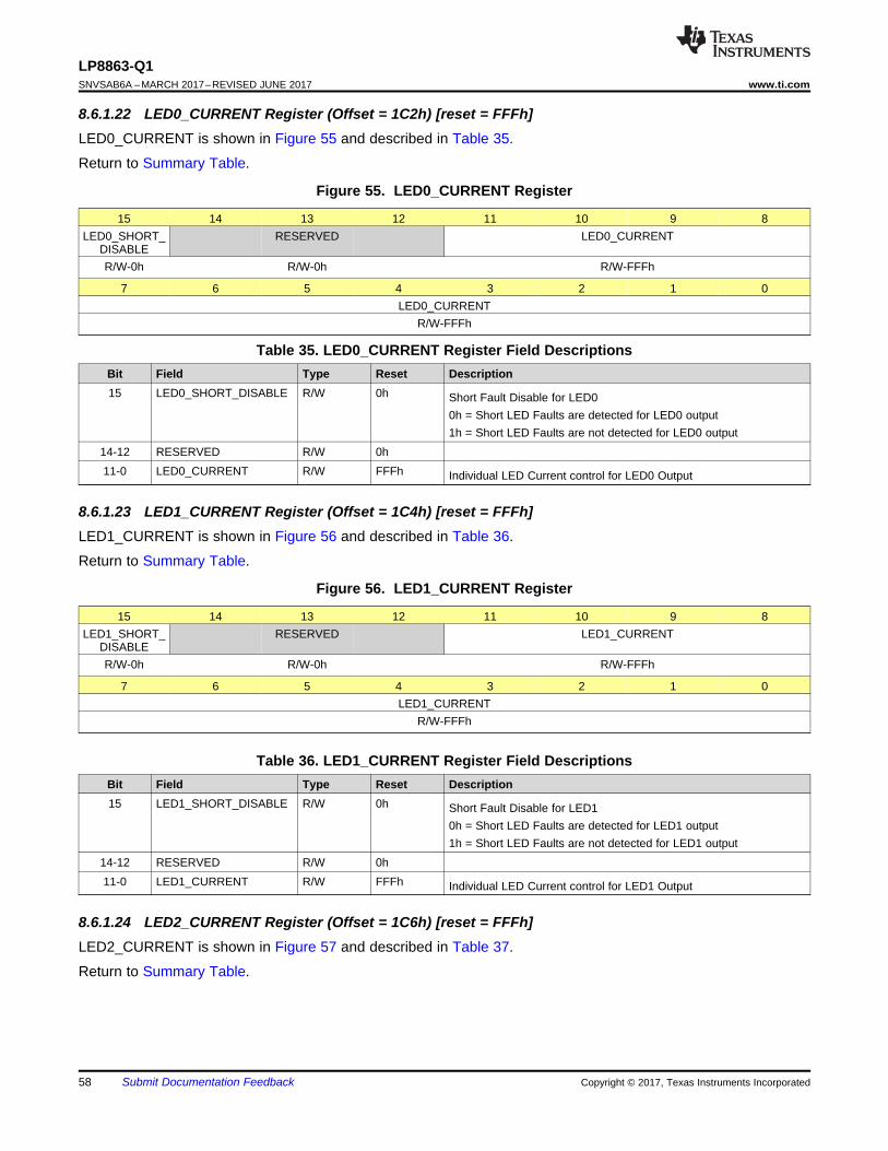
58
LP8863-Q1SNVSAB6A –MARCH 2017–REVISED JUNE 2017 www.ti.com
Submit Documentation Feedback Copyright © 2017, Texas Instruments Incorporated
8.6.1.22 LED0_CURRENT Register (Offset = 1C2h) [reset = FFFh]LED0_CURRENT is shown in Figure 55 and described in Table 35.
Return to Summary Table.
Figure 55. LED0_CURRENT Register
15 14 13 12 11 10 9 8LED0_SHORT_
DISABLERESERVED LED0_CURRENT
R/W-0h R/W-0h R/W-FFFh
7 6 5 4 3 2 1 0LED0_CURRENT
R/W-FFFh
Table 35. LED0_CURRENT Register Field DescriptionsBit Field Type Reset Description15 LED0_SHORT_DISABLE R/W 0h Short Fault Disable for LED0
0h = Short LED Faults are detected for LED0 output1h = Short LED Faults are not detected for LED0 output
14-12 RESERVED R/W 0h11-0 LED0_CURRENT R/W FFFh Individual LED Current control for LED0 Output
8.6.1.23 LED1_CURRENT Register (Offset = 1C4h) [reset = FFFh]LED1_CURRENT is shown in Figure 56 and described in Table 36.
Return to Summary Table.
Figure 56. LED1_CURRENT Register
15 14 13 12 11 10 9 8LED1_SHORT_
DISABLERESERVED LED1_CURRENT
R/W-0h R/W-0h R/W-FFFh
7 6 5 4 3 2 1 0LED1_CURRENT
R/W-FFFh
Table 36. LED1_CURRENT Register Field DescriptionsBit Field Type Reset Description15 LED1_SHORT_DISABLE R/W 0h Short Fault Disable for LED1
0h = Short LED Faults are detected for LED1 output1h = Short LED Faults are not detected for LED1 output
14-12 RESERVED R/W 0h11-0 LED1_CURRENT R/W FFFh Individual LED Current control for LED1 Output
8.6.1.24 LED2_CURRENT Register (Offset = 1C6h) [reset = FFFh]LED2_CURRENT is shown in Figure 57 and described in Table 37.
Return to Summary Table.

59
LP8863-Q1www.ti.com SNVSAB6A –MARCH 2017–REVISED JUNE 2017
Submit Documentation FeedbackCopyright © 2017, Texas Instruments Incorporated
Figure 57. LED2_CURRENT Register
15 14 13 12 11 10 9 8LED2_SHORT_
DISABLERESERVED LED2_CURRENT
R/W-0h R/W-0h R/W-FFFh
7 6 5 4 3 2 1 0LED2_CURRENT
R/W-FFFh
Table 37. LED2_CURRENT Register Field DescriptionsBit Field Type Reset Description15 LED2_SHORT_DISABLE R/W 0h Short Fault Disable for LED2
0h = Short LED Faults are detected for LED2 output1h = Short LED Faults are not detected for LED2 output
14-12 RESERVED R/W 0h11-0 LED2_CURRENT R/W FFFh Individual LED Current control for LED2 Output
8.6.1.25 LED3_CURRENT Register (Offset = 1C8h) [reset = FFFh]LED3_CURRENT is shown in Figure 58 and described in Table 38.
Return to Summary Table.
Figure 58. LED3_CURRENT Register
15 14 13 12 11 10 9 8LED3_SHORT_
DISABLERESERVED LED3_CURRENT
R/W-0h R/W-0h R/W-FFFh
7 6 5 4 3 2 1 0LED3_CURRENT
R/W-FFFh
Table 38. LED3_CURRENT Register Field DescriptionsBit Field Type Reset Description15 LED3_SHORT_DISABLE R/W 0h Short Fault Disable for LED3
0h = Short LED Faults are detected for LED3 output1h = Short LED Faults are not detected for LED3 output
14-12 RESERVED R/W 0h11-0 LED3_CURRENT R/W FFFh Individual LED Current control for LED3 Output
8.6.1.26 LED4_CURRENT Register (Offset = 1CAh) [reset = FFFh]LED4_CURRENT is shown in Figure 59 and described in Table 39.
Return to Summary Table.
Figure 59. LED4_CURRENT Register
15 14 13 12 11 10 9 8LED4_SHORT_
DISABLERESERVED LED4_CURRENT
R/W-0h R/W-0h R/W-FFFh
7 6 5 4 3 2 1 0LED4_CURRENT
R/W-FFFh

60
LP8863-Q1SNVSAB6A –MARCH 2017–REVISED JUNE 2017 www.ti.com
Submit Documentation Feedback Copyright © 2017, Texas Instruments Incorporated
Table 39. LED4_CURRENT Register Field DescriptionsBit Field Type Reset Description15 LED4_SHORT_DISABLE R/W 0h Short Fault Disable for LED4
0h = Short LED Faults are detected for LED4 output1h = Short LED Faults are not detected for LED4 output
14-12 RESERVED R/W 0h11-0 LED4_CURRENT R/W FFFh Individual LED Current control for LED4 Output
8.6.1.27 LED5_CURRENT Register (Offset = 1CCh) [reset = FFFh]LED5_CURRENT is shown in Figure 60 and described in Table 40.
Return to Summary Table.
Figure 60. LED5_CURRENT Register
15 14 13 12 11 10 9 8LED5_SHORT_
DISABLERESERVED LED5_CURRENT
R/W-0h R/W-0h R/W-FFFh
7 6 5 4 3 2 1 0LED5_CURRENT
R/W-FFFh
Table 40. LED5_CURRENT Register Field DescriptionsBit Field Type Reset Description15 LED5_SHORT_DISABLE R/W 0h Short Fault Disable for LED5
0h = Short LED Faults are detected for LED5 output1h = Short LED Faults are not detected for LED5 output
14-12 RESERVED R/W 0h11-0 LED5_CURRENT R/W FFFh Individual LED Current control for LED5 Output
8.6.1.28 BOOST_CONTROL Register (Offset = 288h) [reset = 0h]BOOST_CONTROL is shown in Figure 61 and described in Table 41.
Return to Summary Table.
Figure 61. BOOST_CONTROL Register
15 14 13 12 11 10 9 8LED_EXT_SUPPLY RESERVED
R/W-0h R/W-0h
7 6 5 4 3 2 1 0RESERVED
R/W-0h

61
LP8863-Q1www.ti.com SNVSAB6A –MARCH 2017–REVISED JUNE 2017
Submit Documentation FeedbackCopyright © 2017, Texas Instruments Incorporated
Table 41. BOOST_CONTROL Register Field DescriptionsBit Field Type Reset Description
15-10 LED_EXT_SUPPLY R/W 0h Selects whether external LED voltage supply is used for a LEDoutput.Bit 15 = LED5Bit 14 = LED4Bit 13 = LED3Bit 12 = LED2Bit 11 = LED1Bit 10 = LED00h = LP8863-Q1 Boost Converter Supply is used1h = External Supply is used.
9-0 RESERVED R/W 0h These bits are reserved.
8.6.1.29 SHORT_THRESH Register (Offset = 28Ah) [reset = 882h]SHORT_THRESH is shown in Figure 62 and described in Table 42.
Return to Summary Table.
Figure 62. SHORT_THRESH Register
15 14 13 12 11 10 9 8RESERVED SHORTED_LED_THRESHOLD RESERVED
R/W-0h R/W-4h R/W-82h
7 6 5 4 3 2 1 0RESERVED
R/W-82h
Table 42. SHORT_THRESH Register Field DescriptionsBit Field Type Reset Description
15-12 RESERVED R/W 0h This bit is reserved.11-9 SHORTED_LED_THRES
HOLDR/W 4h Threshold for detecting Shorted LED Fault on LED outputs.
Fault is detected when LEDx pin voltage (referenced to ground)exceeds selected threshold when LED driver is enabled.0h = 2.6 V1h = 3 V2h = 3.4 V3h = 3.8 V4h = 4.2 V5h = 4.8 V6h = 5.2 V7h = 6 V
8-0 RESERVED R/W 82h These bits are reserved.
8.6.1.30 FSM_DIAGNOSTICS Register (Offset = 2A4h) [reset = 0h]FSM_DIAGNOSTICS is shown in Figure 63 and described in Table 43.
Return to Summary Table.
Figure 63. FSM_DIAGNOSTICS Register
15 14 13 12 11 10 9 8RESERVED
R-0h

62
LP8863-Q1SNVSAB6A –MARCH 2017–REVISED JUNE 2017 www.ti.com
Submit Documentation Feedback Copyright © 2017, Texas Instruments Incorporated
7 6 5 4 3 2 1 0RESERVED FSM_LIVE_STATUS
R-0h R-0h
Table 43. FSM_DIAGNOSTICS Register Field DescriptionsBit Field Type Reset Description
15-5 RESERVED R 0h These bits are reserved.4-0 FSM_LIVE_STATUS R 0h Current status of Device state machine.
1h = LDO_STARTUP2h = EEPROM_READ3h = STANDBY4h = BOOST_START5h = BOOST_START6h = BOOST_START7h = ACTIVE
8.6.1.31 PWM_INPUT_DIAGNOSTICS Register (Offset = 2A6h) [reset = 0h]PWM_INPUT_DIAGNOSTICS is shown in Figure 64 and described in Table 44.
Return to Summary Table.
Figure 64. PWM_INPUT_DIAGNOSTICS Register
15 14 13 12 11 10 9 8 7 6 5 4 3 2 1 0PWM_INPUT_STATUS
R-0h
Table 44. PWM_INPUT_DIAGNOSTICS Register Field DescriptionsBit Field Type Reset Description
15-0 PWM_INPUT_STATUS R 0h 16-bit value for detected duty cycle of PWM input signal.
8.6.1.32 PWM_OUTPUT_DIAGNOSTICS Register (Offset = 2A8h) [reset = 0h]PWM_OUTPUT_DIAGNOSTICS is shown in Figure 65 and described in Table 45.
Return to Summary Table.
Figure 65. PWM_OUTPUT_DIAGNOSTICS Register
15 14 13 12 11 10 9 8 7 6 5 4 3 2 1 0LED_PWM_STATUS
R-0h
Table 45. PWM_OUTPUT_DIAGNOSTICS Register Field DescriptionsBit Field Type Reset Description
15-0 LED_PWM_STATUS R 0h 16-bit PWM Duty Code that Brightness path is driving to LED0output.
8.6.1.33 LED_CURR_DIAGNOSTICS Register (Offset = 2AAh) [reset = 0h]LED_CURR_DIAGNOSTICS is shown in Figure 66 and described in Table 46.
Return to Summary Table.

63
LP8863-Q1www.ti.com SNVSAB6A –MARCH 2017–REVISED JUNE 2017
Submit Documentation FeedbackCopyright © 2017, Texas Instruments Incorporated
Figure 66. LED_CURR_DIAGNOSTICS Register
15 14 13 12 11 10 9 8RESERVED LED_CURRENT_STATUS
R-0h R-0h
7 6 5 4 3 2 1 0LED_CURRENT_STATUS
R-0h
Table 46. LED_CURR_DIAGNOSTICS Register Field DescriptionsBit Field Type Reset Description
15-12 RESERVED R 0h These bits are reserved.11-0 LED_CURRENT_STATU
SR 0h 12-bit Current DAC Code that Brightness path is driving to LED0
output.
8.6.1.34 ADAPT_BOOST_DIAGNOSTICS Register (Offset = 2ACh) [reset = 0h]ADAPT_BOOST_DIAGNOSTICS is shown in Figure 67 and described in Table 47.
Return to Summary Table.
Figure 67. ADAPT_BOOST_DIAGNOSTICS Register
15 14 13 12 11 10 9 8RESERVED VBOOST_STATUS
R-0h R-0h
7 6 5 4 3 2 1 0VBOOST_STATUS
R-0h
Table 47. ADAPT_BOOST_DIAGNOSTICS Register Field DescriptionsBit Field Type Reset Description
15-11 RESERVED R 0h These bits are reserved.10-0 VBOOST_STATUS R 0h 11-bit Boost Voltage Code that Adaptive Voltage Control Loop is
sending to Analog Boost Block.Boost Output Voltage =((R_FB1/R_FB2)*1.2)+(R_FB1*18.75nA*VBOOST_STATUS)
8.6.1.35 AUTO_DETECT_DIAGNOSTICS Register (Offset = 2AEh) [reset = 0h]AUTO_DETECT_DIAGNOSTICS is shown in Figure 68 and described in Table 48.
Return to Summary Table.
Figure 68. AUTO_DETECT_DIAGNOSTICS Register
15 14 13 12 11 10 9 8RESERVED AUTO_PWM_F
REQ_SELR-0h R-0h
7 6 5 4 3 2 1 0AUTO_PWM_FREQ_SEL AUTO_BOOST_FREQ_SEL AUTO_LED_STRING_CFG
R-0h R-0h R-0h

64
LP8863-Q1SNVSAB6A –MARCH 2017–REVISED JUNE 2017 www.ti.com
Submit Documentation Feedback Copyright © 2017, Texas Instruments Incorporated
Table 48. AUTO_DETECT_DIAGNOSTICS Register Field DescriptionsBit Field Type Reset Description
15-9 RESERVED R 0h These bits are reserved.8-6 AUTO_PWM_FREQ_SEL R 0h PWM Frequency Setting based on PWM_FSET resistor detection.
0h = 152 Hz1h = 305 Hz2h = 610 Hz3h = 1.22 kHz4h = 2.44 kHz5h = 4.88 kHz6h = 9.77 kHz7h = 19.53 kHz
5-3 AUTO_BOOST_FREQ_SEL
R 0h Boost Frequency Setting based on BST_FSET resistor detection.0h = 303 kHz1h = 400 kHz2h = 606 kHz3h = 800 kHz4h = 1 MHz5h = 1.25 MHz6h = 1.67 MHz7h = 2.2 MHz
2-0 AUTO_LED_STRING_CFG
R 0h Detected LED string configuration.0h = 6 separate strings1h = 5 separate strings2h = 4 separate strings3h = 3 separate strings4h = 2 separate strings5h = outputs connected in groups of 2 to drive 3 strings6h = outputs connected in groups of 3 to drive 2 strings7h = all outputs connected together to drive one string

65
LP8863-Q1www.ti.com SNVSAB6A –MARCH 2017–REVISED JUNE 2017
Submit Documentation FeedbackCopyright © 2017, Texas Instruments Incorporated
9 Application and Implementation
NOTEInformation in the following applications sections is not part of the TI componentspecification, and TI does not warrant its accuracy or completeness. TI’s customers areresponsible for determining suitability of components for their purposes. Customers shouldvalidate and test their design implementation to confirm system functionality.
9.1 Application InformationThe LP8863-Q1 device is designed for automotive applications, and an input voltage VIN is intended to beconnected to the vehicle battery. Depending on the input voltage, the device may be used in either boost modeor SEPIC mode. The device is internally powered from the VDD pin, and voltage must be in 2.7-V to 5.5-V range.The device has flexible configurability through external components or by an SPI or I2C interface. If the VDDvoltage is not high enough to drive an external nMOSFET gate, an internal charge pump must be used to powerthe gate driver (GD pin).
NOTEFor applications where VIN voltage is below the output voltage, use a boost convertertopology. Maximum operating voltage for VIN is 48 V, and the boost converter can achieveoutput voltage up to 47 V. Conversion ratio of 5.5 (full load) or 10 (half load) must betaken into account. If VIN voltage is expected to be below or above output voltage, aSEPIC converter can be implemented. The SEPIC converter can achieve maximum outputvoltage up to 24 V, and maximum conversion ratio for SEPIC mode is 5.
9.2 Typical Applications
9.2.1 Full Feature Application for Display BacklightFigure 69 shows a full application for the LP8863-Q1 device in a boost topology. It supports 6 LED strings indisplay mode, each at 100 mA, with an automatic 60° phase shift. Brightness control register is used for LEDdimming method through I2C communication. The charge pump is enabled for a 400-kHz boost switchingfrequency with spread spectrum.

Copyright © 2017, Texas Instruments Incorporated
LP8863-Q1
C1P
C1N
CPUMP GD
ISNS
ISNSGND
FB
EN
INT
BST_SYNC
LED0
LED1
LED2
LED3
LED4
LED5
VS
EN
SE
_P
VS
EN
SE
_N SD
PGND
PGND
GD
DISCHARGEVDD
VLDO
VDDIO
IFSEL
SDO_PWM
SDI_SDA
SCLK_SCL
SS_ADDRSEL
GND
ISET
CPUMP
PWM_FSET
BST_FSET
VDD
RISENSEVIN
RSD
L1
COUT
RFB1
VOUT
CIN
D1
RFB2RSENSE
Q2
Q1CPUMP
C2x
CVDD
CLDO
RISET
RPWM
RBST
HOST
I2C
VDDIO
66
LP8863-Q1SNVSAB6A –MARCH 2017–REVISED JUNE 2017 www.ti.com
Submit Documentation Feedback Copyright © 2017, Texas Instruments Incorporated
Typical Applications (continued)
Figure 69. Full Feature Application for Display Backlight
9.2.1.1 Design RequirementsThis typical LED-driver application is designed to meet the parameters listed in Table 49:
Table 49. LP8863-Q1 Full-Feature Design ParametersDESIGN PARAMETER VALUE
VIN voltage range 3 V to 20 VVDD voltage 3.3 VLED strings configuration 6 strings, 7 LEDs in seriesCharge pump EnabledBrightness control I2COutput configuration LED0 to LED5 are in display mode (phase shift 60°)LED string current 100 mABoost frequency 400 kHzInductor 22 µH at 12-A saturation currentRISENSE 20 mΩ
Power-line FET EnabledRSENSE 20 mΩ
Input/Output capacitors CIN and COUT: 2 × 33-µF electrolytic + 2 × 10-µF ceramicSpread spectrum EnabledDischarge function Enabled

OUT(max)LSW(max)
III +
2 1 - D'
67
LP8863-Q1www.ti.com SNVSAB6A –MARCH 2017–REVISED JUNE 2017
Submit Documentation FeedbackCopyright © 2017, Texas Instruments Incorporated
9.2.1.2 Detailed Design Procedure
9.2.1.2.1 Inductor Selection
There are a few things to consider when choosing an inductor: inductance, current rating, and DC resistance(DCR). Table 50 shows recommended inductor values for each operating frequency. The LP8863-Q1 deviceautomatically sets internal boost compensation controls depending on the selected switching frequency.
Table 50. Inductance Values for Boost Switching FrequenciesSW FREQUENCY (kHz) INDUCTANCE (µH)
300 22400 22600 15800 151000 101250 101667 102200 10
The current rating of inductor must be at least 25% higher than maximum boost switching current ISW(max), whichcan be calculated with Equation 12. TI recommends a current rating of 12 A for most applications; use aninductor with low DCR to achieve good efficiency. Efficiency varies with load condition, switching frequency, andcomponents, but 80% can be use as safe estimation. Power Stage Designer™ Tools can be used for the boostcalculation: http://www.ti.com/tool/powerstage-designer
where• ΔIL = VIN(min) × D / ƒSW × L• D = 1 – VIN(min) × η / VOUT
• ISW(max): Maximum switching current• ΔIL: Inductor ripple current• IOUT(max): Maximum output current• D: Boost duty cycle• VIN(min): Minimum input voltage• ƒSW: Minimum switching frequency of the converter• L: Inductance• VOUT: Output voltage• η: Efficiency of boost converter (12)
9.2.1.2.2 Output Capacitor Selection
Recommended voltage rating for output capacitors is 50% higher than maximum output voltage level — 100-Vvoltage rating is recommended. Capacitance value determines voltage ripple and boost stability. The DC-biaseffect can reduce the effective capacitance significantly, by up to 80%, a consideration for capacitance valueselection. Effective capacitance must be at least 50 µF for full load/maximum conversion ratio applications andmust be used to achieve good phase and gain margin levels. TI recommends using two 33-µF Al-polymerelectrolytic capacitors and two 10-µF ceramic capacitors in parallel to reduce ripple, increase stability, andreduce ESR effect.
9.2.1.2.3 Input Capacitor Selection
Recommended input capacitance is the same as output capacitance although input capacitors are not as criticalto boost operation. Input capacitance can be reduced but must ensure enough filtering for input power.

mVSENSE
BOOST _ OCP
200R
I
68
LP8863-Q1SNVSAB6A –MARCH 2017–REVISED JUNE 2017 www.ti.com
Submit Documentation Feedback Copyright © 2017, Texas Instruments Incorporated
9.2.1.2.4 Charge Pump Output Capacitor
TI recommends a ceramic capacitor with at least 16-V voltage rating for the output capacitor of the charge pump.A 10-μF capacitor can be used for most applications.
9.2.1.2.5 Charge Pump Flying Capacitor
TI recommends a ceramic capacitor with at least 16-V voltage rating for the flying capacitor of the charge pump.One 2.2-μF capacitor connecting C1P and C1N pins can be used for most applications.
9.2.1.2.6 Output Diode
A Schottky diode must be used for the boost output diode. Current rating must be at least 25% higher than themaximum output current; TI recommends a 12-A current rating for most applications. Schottky diodes with a lowforward drop and fast switching speeds are ideal for increasing efficiency. At maximum current, the forwardvoltage must be as low as possible; less than 0.5 V is recommended. Reverse breakdown voltage of theSchottky diode must be significantly larger than the output voltage, 25% higher voltage rating is recommended.Do not use ordinary rectifier diodes, because slow switching speeds and long recovery times cause efficiencyand load regulation to suffer.
9.2.1.2.7 Switching FET
Gate-drive voltage for the FET is VDD with charge pump bypassed, or about double VDD, if the charge pump isenabled. Switching FET is a critical component for determining power efficiency of the boost converter. Severalaspects need to be considered when selecting switching FET such as voltage and current rating, RDSON, powerdissipation, thermal resistance and rise/fall times. An N type MOSFET with at least 25% higher voltage ratingthan maximum output voltage must be used. Current rating of switching FET should be same or higher thaninductor rating. RDSON must be as low as possible, less than 20 mΩ is recommended. Thermal resistance (RθJA)must also be low to dissipate heat from power loss on switching FET. TI recommends typical rise/fall time valuesless than 10 ns.
9.2.1.2.8 Boost Sense Resistor
The RSENSE resistor determines the boost overcurrent limit and is sensed every boost switching cycle. A high-power 20-mΩ resistor can be used for sensing the boost SW current and setting maximum current limit at 10 A(typical). RSENSE can be increased to lower this limit and can be calculated with Equation 13, but this should bedone carefully because it may also affect stability. Boost overcurrent limit must not be set below 4 A, thereforeRSENSE must not exceed 50 mΩ. Power rating can be calculated from the inductor current and sense resistorresistance value.
where• RSENSE: boost sense resistor (mΩ)• IBOOST_OCP: boost overcurrent limit (13)
9.2.1.2.9 Power-Line FET
A power line FET can be used to disconnect input power from boost input to protect the LP8863-Q1 device andboost components in case an overcurrent event occurs. A P type MOSFET is used for the power-line FET.Voltage rating must be at least 25% higher than maximum input voltage level. Low RDSON is important to reducepower loss on the FET — less than 20 mΩ is recommended. Current rating for the FET must be at least 25%higher than input peak current. Gate-to-source voltage (VGS) for open transistor must be less than minimum inputvoltage; use a 20-kΩ resistor between the pFET gate and source.
9.2.1.2.10 Input Current Sense Resistor
A high-power resistor can be used for sensing the boost input current. Overcurrent condition is detected whenthe voltage across RISENSE reaches 220 mV. Typical 20 mΩ sense resistor is used to set 11-A input current limit.Sense resistor value can be increased to lower overcurrent limit for application as needed. Power rating can becalculated from the input current and resistance value.

Copyright © 2017, Texas Instruments Incorporated
LP8863-Q1
C1P
C1N
CPUMP GD
ISNS
ISNSGND
FB
EN
INT
BST_SYNC
LED0
LED1
LED2
LED3
LED4
LED5
VS
EN
SE
_P
VS
EN
SE
_N SD
PGND
PGND
GD
DISCHARGEVDD
VLDO
VDDIO
IFSEL
SDO_PWM
SDI_SDA
SCLK_SCL
SS_ADDRSEL
GND
ISET
CPUMP
PWM_FSET
BST_FSET
VDD
RISENSEVIN
RSD
L1
COUT
RFB1
VOUT
CIN
D1
RFB2RSENSE
Q2
Q1CPUMP
C2x
CVDD
CLDO
RISET
RPWM
RBST
HOST
I2C
VDDIO
BGOUT_MAX SEL_MAX FB1 BG
FB2
VV = + I R + V
R
·§u¸¨
© ¹
69
LP8863-Q1www.ti.com SNVSAB6A –MARCH 2017–REVISED JUNE 2017
Submit Documentation FeedbackCopyright © 2017, Texas Instruments Incorporated
9.2.1.2.11 Feedback Resistor Divider
Feedback resistors RFB1 and RFB2 determine the maximum boost output level. Output voltage can be calculatedas in Equation 14:
where• VBG = 1.21 V• ISEL_MAX = 38.7 µA• RFB2 = 100 kΩ (recommended for boost mode) (14)
9.2.1.2.12 Critical Components for Design
Figure 70 shows the critical part of circuitry: boost components, the LP8863-Q1 internal charge pump for gate-driver powering, and powering/grounding of LP8863-Q1. Schematic example is shown in Figure 70.
Figure 70. Critical Components for Full Feature Design

70
LP8863-Q1SNVSAB6A –MARCH 2017–REVISED JUNE 2017 www.ti.com
Submit Documentation Feedback Copyright © 2017, Texas Instruments Incorporated
Table 51. Recommended Component Values for Full Feature Design ExampleREFERENCEDESIGNATOR
DESCRIPTION NOTE
RISENSE 20 mΩ, 3 W Input current sensing resistorRSD 20 kΩ, 0.1 W Power-line FET gate pullup resistor
RSENSE 20 mΩ, 3 W Boost current sensing resistorRFB2 100 kΩ, 0.1 W Bottom feedback divider resistorRFB1 910 kΩ, 0.1 W Top feedback divider resistorRBST 4.77 kΩ, 0.1 W Boost frequency set resistorRISET 31.2 kΩ, 0.1 W Maximum current set resistorRPWM 42.2 kΩ, 0.1 W Output PWM frequency set resistorCPUMP 10-µF, 16-V ceramic Charge-pump output capacitor
C2X 2.2-µF, 25-V ceramic Flying capacitorCVDD 4.7-µF + 0.1-µF, 10-V ceramic VDD bypass capacitorCLDO 4.7-µF + 0.1-µF, 10-V ceramic VLDO bypass capacitorCIN 2 × 33-µF, 63-V electrolytic + 2 × 10-µF, 100-V ceramic Boost input capacitor
COUT 2 × 33-µF, 63-V electrolytic + 2 × 10-µF, 100-V ceramic Boost output capacitorL1 22-μH saturation current 23 A Boost inductorD1 100 V, 10-A Schottky diode Boost Schottky diodeQ1 60-V, 25-A nMOSFET Boost nMOSFETQ2 60-V, 30-A pMOSFET Power-line FET
9.2.1.3 Application Curves
FLED_PWM = 300 Hz Phase Shift 60° 6 Strings
Figure 71. LED String Currents Showing Phase Shift PWMOperation
ƒSW = 400 kHz 100 mA/StringCIN = COUT = 2 × 33 μF (electrolytic) + 2 × 10 μF (ceramic)
Figure 72. Typical Start-Up

Copyright © 2017, Texas Instruments Incorporated
LP8863-Q1
C1P
C1N
CPUMP GD
ISNS
ISNSGND
FB
EN
INT
BST_SYNC
LED0
LED1
LED2
LED3
LED4
LED5
VS
EN
SE
_P
VS
EN
SE
_N SD
PGND
PGND
GD
DISCHARGEVDD
VLDO
VDDIO
IFSEL
SDO_PWM
SDI_SDA
SCLK_SCL
SS_ADDRSEL
GND
ISET
CPUMP
PWM_FSET
BST_FSET
L1 D1
Q1
VDD
VINL1
COUT
RFB1
CIN
D1
RFB2RSENSE
CPUMP
CVDD
CLDO
RISET
RPWM
RBST
VOUT
RFB3
71
LP8863-Q1www.ti.com SNVSAB6A –MARCH 2017–REVISED JUNE 2017
Submit Documentation FeedbackCopyright © 2017, Texas Instruments Incorporated
9.2.2 Application With Basic/Minimal OperationThe LP8863-Q1 needs only a few external components for basic functionality if material cost and PCB area for asolution need to be minimized. In this example LP8863-Q1 is configured with external components and no I2C orSPI communication. The power-line FET is removed, as is input current sensing. Internal charge pump is notused, and all external synchronization functions and special features are disabled. Only 5 LED strings areenabled.
Figure 73. Minimal Solution/Minimum Components Application
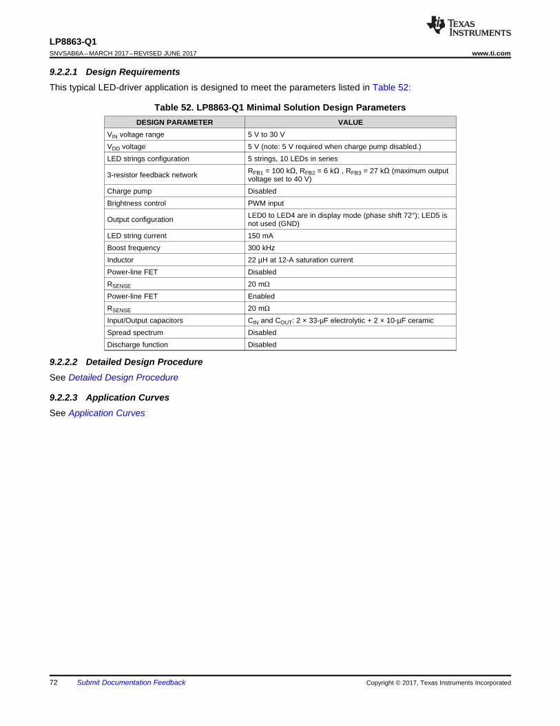
72
LP8863-Q1SNVSAB6A –MARCH 2017–REVISED JUNE 2017 www.ti.com
Submit Documentation Feedback Copyright © 2017, Texas Instruments Incorporated
9.2.2.1 Design RequirementsThis typical LED-driver application is designed to meet the parameters listed in Table 52:
Table 52. LP8863-Q1 Minimal Solution Design ParametersDESIGN PARAMETER VALUE
VIN voltage range 5 V to 30 VVDD voltage 5 V (note: 5 V required when charge pump disabled.)LED strings configuration 5 strings, 10 LEDs in series
3-resistor feedback network RFB1 = 100 kΩ, RFB2 = 6 kΩ , RFB3 = 27 kΩ (maximum outputvoltage set to 40 V)
Charge pump DisabledBrightness control PWM input
Output configuration LED0 to LED4 are in display mode (phase shift 72°); LED5 isnot used (GND)
LED string current 150 mABoost frequency 300 kHzInductor 22 µH at 12-A saturation currentPower-line FET DisabledRSENSE 20 mΩ
Power-line FET EnabledRSENSE 20 mΩ
Input/Output capacitors CIN and COUT: 2 × 33-µF electrolytic + 2 × 10-µF ceramicSpread spectrum DisabledDischarge function Disabled
9.2.2.2 Detailed Design ProcedureSee Detailed Design Procedure
9.2.2.3 Application CurvesSee Application Curves

Copyright © 2017, Texas Instruments Incorporated
LP8863-Q1
C1P
C1N
CPUMP GD
ISNS
ISNSGND
FB
EN
INT
BST_SYNC
LED0
LED1
LED2
LED3
LED4
LED5
VS
EN
SE
_P
VS
EN
SE
_N SD
PGND
PGND
GD
DISCHARGEVDD
VLDO
VDDIO
IFSEL
SDO_PWM
SDI_SDA
SCLK_SCLSS_ADDRSEL
GND
ISET
CPUMP
PWM_FSET
BST_FSET
RISENSE L1 D1Q2
Q1
HOST
SPI
CS1
CS2 RS
L2
VDD
VIN
RSD
L1
COUT
RFB1
CIN
RFB2RSENSE
Q2
CPUMP
C2x
CVDD
CLDO
RISET
RPWM
RBST
VOUT
73
LP8863-Q1www.ti.com SNVSAB6A –MARCH 2017–REVISED JUNE 2017
Submit Documentation FeedbackCopyright © 2017, Texas Instruments Incorporated
9.2.3 SEPIC Mode ApplicationWhen LED string voltage can be above and below the input voltage level, use the SEPIC configuration. In SEPICmode, the SW pin detects a maximum voltage equal to the sum of the input and output voltages, a considerationwhen selecting components. This fact limits the maximum output voltage to 24 V. External frequency can beused to synchronize boost or SEPIC switching frequency through the BST_SYNC pin.
Figure 74. SEPIC Mode with Three LEDs in Series
74
LP8863-Q1SNVSAB6A –MARCH 2017–REVISED JUNE 2017 www.ti.com
Submit Documentation Feedback Copyright © 2017, Texas Instruments Incorporated
9.2.3.1 Design RequirementsThis typical LED-driver application is designed to meet the parameters listed in Table 53:
Table 53. LP8863-Q1 SEPIC Mode Design ParametersDESIGN PARAMETER VALUE
VIN voltage range 3 V to 48 VVDD voltage 3.3 VLED strings configuration 6 strings, 3 LEDs in seriesCharge pump EnabledBrightness control SPIOutput configuration LED0 to LED5 are in display mode (phase shift 60°)LED string current 150 mA
BST_SYNC external signal frequency 2.2 MHz (Note: BST_SYNC frequency must be 0.2 to 0.5%higher than frequency set by BST_FSET resistor.)
BST_FSET resistor 42.2 kΩ (sets boost frequency to 1.6 MHz)Inductor 10 µH at 12-A saturation currentRISENSE 20 mΩ
Power-line FET EnabledRSENSE 20 mΩ
Input/Output capacitors CIN and COUT: 2 × 33-µF electrolytic + 2 × 10-µF ceramicSpread spectrum DisabledDischarge function EnabledBoost synchronization Enabled
.
9.2.3.2 Detailed Design Procedure
9.2.3.2.1 Inductor Selection
Inductance for both inductors can be selected from Table 54, depending on operating frequency for theapplication. Current rating is recommended to be at least 25% higher than maximum inductor peak current.Peak-to-peak ripple current can be estimated to be approximately 40% of the maximum input current and andinductor peak current can be calculated with Equation 15, Equation 16, and Equation 17:
Table 54. Inductance Values for SEPIC SwitchingFrequencies
SW FREQUENCY (kHz) INDUCTANCE (µH)300 15400 15600 10800 101000 6.81250 6.81667 4.72200 4.7

OUT DCs(rms) OUT
IN(min)
V VI = I
V
u
OUTL IN OUT
IN(min)
VI = I 40% = I 40%
V' u u u
L2(peak) OUT40%
I = I 1 + 2
·§u ¨ ¸© ¹
OUT DL1(peak) OUT
IN(min)
V V 40%I = I 1 +
V 2 ·§
u u ¨ ¸© ¹
75
LP8863-Q1www.ti.com SNVSAB6A –MARCH 2017–REVISED JUNE 2017
Submit Documentation FeedbackCopyright © 2017, Texas Instruments Incorporated
where• IL1(peak): Peak current for inductor 1• IOUT: Maximum output current• VOUT: Output voltage• VD: Diode forward voltage drop• VIN(min): Minimum input voltage (15)
where• IL2(peak): Peak current for inductor 2• IOUT: Maximum output current (16)
where• ΔIL: Inductor ripple current• IIN: Input current• VOUT: Output voltage• VIN(min): Minimum input voltage (17)
9.2.3.2.2 Coupling Capacitor Selection
The coupling capacitors Cs isolate the input from the output and provide protection against a shorted load. Theselection of SEPIC capacitors, Cs, depends mostly on the RMS current, which can be calculated withEquation 18. The capacitors must be rated for a large RMS current relative to the output power; TI recommendsat least 25% higher rating for IRMS. When using uncoupled inductors, use one 10-µH ceramic capacitor in parallelwith one 33-µF electrolytic capacitor and series 2-Ω resistor. If coupled inductors are used, then use only one 10-µF ceramic capacitor.
where• ICs(rms): RMS current of Cs capacitor• IOUT: Output current• VOUT: Output voltage• VD: Diode forward voltage drop• VIN(min): Minimum input voltage (18)
9.2.3.2.3 Output Capacitor Selection
See Detailed Design Procedure
9.2.3.2.4 Input Capacitor Selection
See Detailed Design Procedure
9.2.3.2.5 Charge Pump Output Capacitor
See Detailed Design Procedure
9.2.3.2.6 Charge Pump Flying Capacitor
See Detailed Design Procedure
BGOUT _MAX SEL_MAX FB1 BG
FB2
V V = + I R + V
R
·§u¸¨
© ¹
Q1(peak) L1(peak) L2(peak)I = I I
76
LP8863-Q1SNVSAB6A –MARCH 2017–REVISED JUNE 2017 www.ti.com
Submit Documentation Feedback Copyright © 2017, Texas Instruments Incorporated
9.2.3.2.7 Switching FET
Gate-drive voltage for the FET is VDD or about 2 × VDD, if the charge pump is enabled. Use an N-type MOSFETfor the switching FET. The switching FET for SEPIC mode sees a maximum voltage of VIN(max) + VOUT, 25%higher rating is recommended. Current rating is also recommended to be 25% higher than peak current, whichcan be calculated with Equation 19. RDSON must be as low as possible — less than 20 mΩ is recommended.Thermal resistance (RθJA) must also be low to dissipate heat from power loss on switching FET. Typical rise/falltime values recommended are less than 10 ns.
where• IQ1(peak): Peak current for switching FET• IL1(peak): Peak current for inductor 1• IIL2(peak): : Peak current for inductor 2 BOOST_OCP (19)
9.2.3.2.8 Output Diode
A Schottky diode must be used for the SEPIC output diode. Current rating must be at least 25% higher than themaximum current, which is the same as switch peak current. Schottky diodes with a low forward drop and fastswitching speeds are ideal for increasing efficiency. At maximum current, the forward voltage must be as low aspossible; TI recommends less than 0.5 V. Reverse breakdown voltage of the Schottky diode must be able towithstand VIN(max) + VOUT(max); at least 25% higher voltage rating is recommended. Do not use ordinary rectifierdiodes, because slow switching speeds and long recovery times cause efficiency and load regulation to suffer.
9.2.3.2.9 Switching Sense Resistor
See Detailed Design Procedure
9.2.3.2.10 Power-Line FET
See Detailed Design Procedure
9.2.3.2.11 Input Current Sense Resistor
See Detailed Design Procedure
9.2.3.2.12 Feedback Resistor Divider
Feedback resistors RFB1 and RFB2 determine the maximum boost output level. Output voltage can be calculatedas follows:
where• VBG = 1.21 V• ISEL_MAX = 38.7 µA• RFB2 = 170 kΩ (recommended for SEPIC Mode) (20)
9.2.3.2.13 Critical Components for Design
Figure 75 shows the critical part of circuitry: SEPIC components, the LP8863-Q1 internal charge pump for gate-driver powering, and powering/grounding of LP8863-Q1. Schematic example is shown in Figure 70.

Copyright © 2017, Texas Instruments Incorporated
LP8863-Q1
C1P
C1N
CPUMP GD
ISNS
ISNSGND
FB
EN
INT
BST_SYNC
LED0
LED1
LED2
LED3
LED4
LED5
VS
EN
SE
_P
VS
EN
SE
_N SD
PGND
PGND
GD
DISCHARGEVDD
VLDO
VDDIO
IFSEL
SDO_PWM
SDI_SDA
SCLK_SCLSS_ADDRSEL
GND
ISET
CPUMP
PWM_FSET
BST_FSET
RISENSE L1 D1Q2
Q1
HOST
SPI
CS1
CS2 RS
L2
VDD
VIN
RSD
L1
COUT
RFB1
CIN
RFB2RSENSE
Q2
CPUMP
C2x
CVDD
CLDO
RISET
RPWM
RBST
VOUT
77
LP8863-Q1www.ti.com SNVSAB6A –MARCH 2017–REVISED JUNE 2017
Submit Documentation FeedbackCopyright © 2017, Texas Instruments Incorporated
Figure 75. Critical Components for SEPIC Mode Design
Table 55. Recommended Components for SEPIC Design ExampleREFERENCE DESIGNATOR DESCRIPTION NOTE
RISENSE 20 mΩ, 3 W Input current sensing resistorRSD 20 kΩ, 0.1 W Power-line FET gate pullup resistor
RSENSE 20 mΩ, 3 W SEPIC current sensing resistorRFB2 170 kΩ, 0.1 W Bottom feedback divider resistorRFB1 560 kΩ, 0.1 W Top feedback divider resistorRBST 140 kΩ, 0.1 W SEPIC frequency set resistorRISET 20.5 kΩ, 0.1 W Maximum current set resistorRPWM 140 kΩ, 0.1 W Output PWM frequency set resistorCPUMP 10-µF, 16-V ceramic Charge pump output capacitor
C2x 2.2-µF, 25-V ceramic Flying capacitorCVDD 4.7-µF + 0.1-µF, 10-V ceramic VDD bypass capacitorCLDO 10-µF + 0.1-µF, 10-V ceramic VLDO bypass capacitorCIN 2 × 33-µF, 63-V electrolytic SEPIC input capacitor
COUT 2 × 33-µF, 63-V electrolytic SEPIC output capacitorCS1 10-µF, 100-V ceramic SEPIC coupling capacitorCS2 33-µF, 63-V electrolytic SEPIC coupling capacitorRS 2 Ω, 0.125 W SEPIC resistorL1 10-µH saturation current 15.5 A SEPIC inductorL2 10-µH saturation current 15.5 A SEPIC inductorD1 100-V 10-A Schottky diode SEPIC Schottky diodeQ1 60-V, 25-A nMOSFET SEPIC nMOSFETQ2 60-V, 30-A pMOSFET Power-line FET

78
LP8863-Q1SNVSAB6A –MARCH 2017–REVISED JUNE 2017 www.ti.com
Submit Documentation Feedback Copyright © 2017, Texas Instruments Incorporated
9.2.3.3 Application CurvesSee Application Curves
10 Power Supply RecommendationsThe LP8863-Q1 is designed to operate from a car battery. The VIN input must be protected from reverse voltageand voltage dump condition over 48 V. The impedance of the input supply rail must be low enough that the inputcurrent transient does not cause drop below VIN UVLO level. If the input supply is connected with long wires,additional bulk capacitance may be required in addition to normal input capacitor.
The voltage range for VDD is 3 V to 5.5 V. A ceramic capacitor must be placed as close as possible to the VDDpin. The boost gate driver is powered from the CPUMP pins. A ceramic capacitor must be placed as close to theCPUMP pins as possible.

79
LP8863-Q1www.ti.com SNVSAB6A –MARCH 2017–REVISED JUNE 2017
Submit Documentation FeedbackCopyright © 2017, Texas Instruments Incorporated
11 Layout
11.1 Layout GuidelinesFigure 76 shows a layout recommendation for the LP8863-Q1 used to illustrate the principles of good layout.This layout can be adapted to the actual application layout if and where possible. It is important that all boostcomponents are close to each other and to the chip; the high-current traces must be wide enough. VDD must beas noise-free as possible. Place a VDD bypass capacitor near the VDD and GND pins and ground it to a low-noise ground. A charge-pump capacitor, boost input capacitors, and boost output capacitors must be connectedto PGND. Place the charge-pump capacitors close to the device. The main points to guide the PCB layoutdesign:• Current loops need to be minimized:
– For low frequency the minimal current loop can be achieved by placing the boost components as close aspossible to each other. Input and output capacitor grounds need to be close to each other to minimizecurrent loop size.
– Minimal current loops for high frequencies can be achieved by making sure that the ground plane is intactunder the current traces. High frequency return currents follow the route with minimum impedance, whichis the route with minimum loop area, not necessarily the shortest path. Minimum loop area is formed whenreturn current flows just under the positive current route in the ground plane, if the ground plane is intactunder the route.
– For high frequency the copper area capacitance must be taken into account. For example, the copperarea for the drain of boost nMOSFET is a tradeoff between capacitance and the cooling capacity of thecomponents.
• GND plane must be intact under the high-current-boost traces to provide shortest possible return path andsmallest possible current loops for high frequencies.
• Current loops when the boost switch is conducting and not conducting must be in the same direction inoptimal case.
• Inductors must be placed so that the current flows in the same direction as in the current loops. Rotating theinductor 180° changes current direction.
• Use separate power and noise-free grounds. PGND is used for boost converter return current. Use a low-noise ground for more sensitive signals, like VDD bypass capacitor grounding as well as grounding the GNDpins of the LP8863-Q1 device itself.
• Route boost output voltage (VOUT) to LEDs from output capacitors not straight from the diode cathode.• A small bypass capacitor (TI recommends a 39-pF capacitor) must be placed close to the FB pin to suppress
high frequency noise• VDD line must be separated from the high current supply path to the boost converter to prevent high
frequency ripple affecting the chip behavior. A separate 1-µF bypass capacitor is used for the VDD pin, and itis grounded to noise-free ground.
• Capacitor connected to charge pump output CPUMP must have 10-µF capacitance, grounded by the shortestway to boost a switch-current-sensing resistor. This capacitor must be as close as possible to CPUMP pin.This capacitor provides a greater peak current for gate driver and must be used even if the charge pump isdisabled. If the charge pump is disabled, the VDD and CPUMP pins must be tied together.
• Input and output capacitors need low-impedence grounding (wide traces with many vias to PGND plane).• If two or more output capacitors are used, symmetrical layout must be used to get all capacitors working
ideally.• Input/output ceramic capacitors have DC-bias effect. If the output capacitance is too low, it can cause boost
to become unstable under certain load conditions. DC bias characteristics should be obtained from thecomponent manufacturer; DC bias is not taken into account on component tolerance. TI recommendsX5R/X7R capacitors.

80
LP8863-Q1SNVSAB6A –MARCH 2017–REVISED JUNE 2017 www.ti.com
Submit Documentation Feedback Copyright © 2017, Texas Instruments Incorporated
11.2 Layout Example
Figure 76. LP8863-Q1 Layout Guidelines

81
LP8863-Q1www.ti.com SNVSAB6A –MARCH 2017–REVISED JUNE 2017
Submit Documentation FeedbackCopyright © 2017, Texas Instruments Incorporated
12 Device and Documentation Support
12.1 Device Support
12.1.1 Third-Party Products DisclaimerTI'S PUBLICATION OF INFORMATION REGARDING THIRD-PARTY PRODUCTS OR SERVICES DOES NOTCONSTITUTE AN ENDORSEMENT REGARDING THE SUITABILITY OF SUCH PRODUCTS OR SERVICESOR A WARRANTY, REPRESENTATION OR ENDORSEMENT OF SUCH PRODUCTS OR SERVICES, EITHERALONE OR IN COMBINATION WITH ANY TI PRODUCT OR SERVICE.
12.2 Receiving Notification of Documentation UpdatesTo receive notification of documentation updates, navigate to the device product folder on ti.com. In the upperright corner, click on Alert me to register and receive a weekly digest of any product information that haschanged. For change details, review the revision history included in any revised document.
12.3 Community ResourcesThe following links connect to TI community resources. Linked contents are provided "AS IS" by the respectivecontributors. They do not constitute TI specifications and do not necessarily reflect TI's views; see TI's Terms ofUse.
TI E2E™ Online Community TI's Engineer-to-Engineer (E2E) Community. Created to foster collaborationamong engineers. At e2e.ti.com, you can ask questions, share knowledge, explore ideas and helpsolve problems with fellow engineers.
Design Support TI's Design Support Quickly find helpful E2E forums along with design support tools andcontact information for technical support.
12.4 TrademarksE2E is a trademark of Texas Instruments.All other trademarks are the property of their respective owners.
12.5 Electrostatic Discharge CautionThese devices have limited built-in ESD protection. The leads should be shorted together or the device placed in conductive foamduring storage or handling to prevent electrostatic damage to the MOS gates.
12.6 GlossarySLYZ022 — TI Glossary.
This glossary lists and explains terms, acronyms, and definitions.
13 Mechanical, Packaging, and Orderable InformationThe following pages include mechanical, packaging, and orderable information. This information is the mostcurrent data available for the designated devices. This data is subject to change without notice and revision ofthis document. For browser-based versions of this data sheet, refer to the left-hand navigation.

PACKAGE OPTION ADDENDUM
www.ti.com 9-Jun-2017
Addendum-Page 1
PACKAGING INFORMATION
Orderable Device Status(1)
Package Type PackageDrawing
Pins PackageQty
Eco Plan(2)
Lead/Ball Finish(6)
MSL Peak Temp(3)
Op Temp (°C) Device Marking(4/5)
Samples
LP8863ADCPRQ1 ACTIVE HTSSOP DCP 38 2000 Green (RoHS& no Sb/Br)
CU NIPDAU Level-3-260C-168 HR -40 to 125 LP8863AQ1
(1) The marketing status values are defined as follows:ACTIVE: Product device recommended for new designs.LIFEBUY: TI has announced that the device will be discontinued, and a lifetime-buy period is in effect.NRND: Not recommended for new designs. Device is in production to support existing customers, but TI does not recommend using this part in a new design.PREVIEW: Device has been announced but is not in production. Samples may or may not be available.OBSOLETE: TI has discontinued the production of the device.
(2) RoHS: TI defines "RoHS" to mean semiconductor products that are compliant with the current EU RoHS requirements for all 10 RoHS substances, including the requirement that RoHS substancedo not exceed 0.1% by weight in homogeneous materials. Where designed to be soldered at high temperatures, "RoHS" products are suitable for use in specified lead-free processes. TI mayreference these types of products as "Pb-Free".RoHS Exempt: TI defines "RoHS Exempt" to mean products that contain lead but are compliant with EU RoHS pursuant to a specific EU RoHS exemption.Green: TI defines "Green" to mean the content of Chlorine (Cl) and Bromine (Br) based flame retardants meet JS709B low halogen requirements of <=1000ppm threshold. Antimony trioxide basedflame retardants must also meet the <=1000ppm threshold requirement.
(3) MSL, Peak Temp. - The Moisture Sensitivity Level rating according to the JEDEC industry standard classifications, and peak solder temperature.
(4) There may be additional marking, which relates to the logo, the lot trace code information, or the environmental category on the device.
(5) Multiple Device Markings will be inside parentheses. Only one Device Marking contained in parentheses and separated by a "~" will appear on a device. If a line is indented then it is a continuationof the previous line and the two combined represent the entire Device Marking for that device.
(6) Lead/Ball Finish - Orderable Devices may have multiple material finish options. Finish options are separated by a vertical ruled line. Lead/Ball Finish values may wrap to two lines if the finishvalue exceeds the maximum column width.
Important Information and Disclaimer:The information provided on this page represents TI's knowledge and belief as of the date that it is provided. TI bases its knowledge and belief on informationprovided by third parties, and makes no representation or warranty as to the accuracy of such information. Efforts are underway to better integrate information from third parties. TI has taken andcontinues to take reasonable steps to provide representative and accurate information but may not have conducted destructive testing or chemical analysis on incoming materials and chemicals.TI and TI suppliers consider certain information to be proprietary, and thus CAS numbers and other limited information may not be available for release.
In no event shall TI's liability arising out of such information exceed the total purchase price of the TI part(s) at issue in this document sold by TI to Customer on an annual basis.

TAPE AND REEL INFORMATION
*All dimensions are nominal
Device PackageType
PackageDrawing
Pins SPQ ReelDiameter
(mm)
ReelWidth
W1 (mm)
A0(mm)
B0(mm)
K0(mm)
P1(mm)
W(mm)
Pin1Quadrant
LP8863ADCPRQ1 HTSSOP DCP 38 2000 330.0 16.4 6.9 10.2 1.8 12.0 16.0 Q1
PACKAGE MATERIALS INFORMATION
www.ti.com 9-Jun-2017
Pack Materials-Page 1

*All dimensions are nominal
Device Package Type Package Drawing Pins SPQ Length (mm) Width (mm) Height (mm)
LP8863ADCPRQ1 HTSSOP DCP 38 2000 367.0 367.0 38.0
PACKAGE MATERIALS INFORMATION
www.ti.com 9-Jun-2017
Pack Materials-Page 2


IMPORTANT NOTICE
Texas Instruments Incorporated (TI) reserves the right to make corrections, enhancements, improvements and other changes to itssemiconductor products and services per JESD46, latest issue, and to discontinue any product or service per JESD48, latest issue. Buyersshould obtain the latest relevant information before placing orders and should verify that such information is current and complete.TI’s published terms of sale for semiconductor products (http://www.ti.com/sc/docs/stdterms.htm) apply to the sale of packaged integratedcircuit products that TI has qualified and released to market. Additional terms may apply to the use or sale of other types of TI products andservices.Reproduction of significant portions of TI information in TI data sheets is permissible only if reproduction is without alteration and isaccompanied by all associated warranties, conditions, limitations, and notices. TI is not responsible or liable for such reproduceddocumentation. Information of third parties may be subject to additional restrictions. Resale of TI products or services with statementsdifferent from or beyond the parameters stated by TI for that product or service voids all express and any implied warranties for theassociated TI product or service and is an unfair and deceptive business practice. TI is not responsible or liable for any such statements.Buyers and others who are developing systems that incorporate TI products (collectively, “Designers”) understand and agree that Designersremain responsible for using their independent analysis, evaluation and judgment in designing their applications and that Designers havefull and exclusive responsibility to assure the safety of Designers' applications and compliance of their applications (and of all TI productsused in or for Designers’ applications) with all applicable regulations, laws and other applicable requirements. Designer represents that, withrespect to their applications, Designer has all the necessary expertise to create and implement safeguards that (1) anticipate dangerousconsequences of failures, (2) monitor failures and their consequences, and (3) lessen the likelihood of failures that might cause harm andtake appropriate actions. Designer agrees that prior to using or distributing any applications that include TI products, Designer willthoroughly test such applications and the functionality of such TI products as used in such applications.TI’s provision of technical, application or other design advice, quality characterization, reliability data or other services or information,including, but not limited to, reference designs and materials relating to evaluation modules, (collectively, “TI Resources”) are intended toassist designers who are developing applications that incorporate TI products; by downloading, accessing or using TI Resources in anyway, Designer (individually or, if Designer is acting on behalf of a company, Designer’s company) agrees to use any particular TI Resourcesolely for this purpose and subject to the terms of this Notice.TI’s provision of TI Resources does not expand or otherwise alter TI’s applicable published warranties or warranty disclaimers for TIproducts, and no additional obligations or liabilities arise from TI providing such TI Resources. TI reserves the right to make corrections,enhancements, improvements and other changes to its TI Resources. TI has not conducted any testing other than that specificallydescribed in the published documentation for a particular TI Resource.Designer is authorized to use, copy and modify any individual TI Resource only in connection with the development of applications thatinclude the TI product(s) identified in such TI Resource. NO OTHER LICENSE, EXPRESS OR IMPLIED, BY ESTOPPEL OR OTHERWISETO ANY OTHER TI INTELLECTUAL PROPERTY RIGHT, AND NO LICENSE TO ANY TECHNOLOGY OR INTELLECTUAL PROPERTYRIGHT OF TI OR ANY THIRD PARTY IS GRANTED HEREIN, including but not limited to any patent right, copyright, mask work right, orother intellectual property right relating to any combination, machine, or process in which TI products or services are used. Informationregarding or referencing third-party products or services does not constitute a license to use such products or services, or a warranty orendorsement thereof. Use of TI Resources may require a license from a third party under the patents or other intellectual property of thethird party, or a license from TI under the patents or other intellectual property of TI.TI RESOURCES ARE PROVIDED “AS IS” AND WITH ALL FAULTS. TI DISCLAIMS ALL OTHER WARRANTIES ORREPRESENTATIONS, EXPRESS OR IMPLIED, REGARDING RESOURCES OR USE THEREOF, INCLUDING BUT NOT LIMITED TOACCURACY OR COMPLETENESS, TITLE, ANY EPIDEMIC FAILURE WARRANTY AND ANY IMPLIED WARRANTIES OFMERCHANTABILITY, FITNESS FOR A PARTICULAR PURPOSE, AND NON-INFRINGEMENT OF ANY THIRD PARTY INTELLECTUALPROPERTY RIGHTS. TI SHALL NOT BE LIABLE FOR AND SHALL NOT DEFEND OR INDEMNIFY DESIGNER AGAINST ANY CLAIM,INCLUDING BUT NOT LIMITED TO ANY INFRINGEMENT CLAIM THAT RELATES TO OR IS BASED ON ANY COMBINATION OFPRODUCTS EVEN IF DESCRIBED IN TI RESOURCES OR OTHERWISE. IN NO EVENT SHALL TI BE LIABLE FOR ANY ACTUAL,DIRECT, SPECIAL, COLLATERAL, INDIRECT, PUNITIVE, INCIDENTAL, CONSEQUENTIAL OR EXEMPLARY DAMAGES INCONNECTION WITH OR ARISING OUT OF TI RESOURCES OR USE THEREOF, AND REGARDLESS OF WHETHER TI HAS BEENADVISED OF THE POSSIBILITY OF SUCH DAMAGES.Unless TI has explicitly designated an individual product as meeting the requirements of a particular industry standard (e.g., ISO/TS 16949and ISO 26262), TI is not responsible for any failure to meet such industry standard requirements.Where TI specifically promotes products as facilitating functional safety or as compliant with industry functional safety standards, suchproducts are intended to help enable customers to design and create their own applications that meet applicable functional safety standardsand requirements. Using products in an application does not by itself establish any safety features in the application. Designers mustensure compliance with safety-related requirements and standards applicable to their applications. Designer may not use any TI products inlife-critical medical equipment unless authorized officers of the parties have executed a special contract specifically governing such use.Life-critical medical equipment is medical equipment where failure of such equipment would cause serious bodily injury or death (e.g., lifesupport, pacemakers, defibrillators, heart pumps, neurostimulators, and implantables). Such equipment includes, without limitation, allmedical devices identified by the U.S. Food and Drug Administration as Class III devices and equivalent classifications outside the U.S.TI may expressly designate certain products as completing a particular qualification (e.g., Q100, Military Grade, or Enhanced Product).Designers agree that it has the necessary expertise to select the product with the appropriate qualification designation for their applicationsand that proper product selection is at Designers’ own risk. Designers are solely responsible for compliance with all legal and regulatoryrequirements in connection with such selection.Designer will fully indemnify TI and its representatives against any damages, costs, losses, and/or liabilities arising out of Designer’s non-compliance with the terms and provisions of this Notice.
Mailing Address: Texas Instruments, Post Office Box 655303, Dallas, Texas 75265Copyright © 2017, Texas Instruments Incorporated