lower protrusion of a copper-nickel alloy in a through ... · lower protrusion of a copper-nickel...
TRANSCRIPT

Lower Protrusion of a Copper-Nickel Alloy in a Through-Silicon viaand Its Numerical Simulation
Hoon Sun Jung1, Young-Joo Jang2, Sung-Hoon Choa1,+ and Jae Pil Jung2,+
1Graduate School of NID Fusion Technology, Seoul National University of Science and Technology,Seoul 139-743, Republic of Korea2Department of Materials Science and Engineering, University of Seoul, Seoul 130-743, Korea
The application of Cu-filled through-silicon via (TSV) in 3-D integrated circuit packaging faces several fabrication and reliability issues. Inthis study, we introduced a Cu-Ni alloy for TSV filling with a high filling speed and a reduced TSV protrusion. In particular, the characteristics ofCu-Ni via protrusions at various annealing temperatures (³200450°C) were investigated with experimental and numerical analysis andcompared with Cu-filled vias. High speed Cu-Ni alloy filling into the vias was achieved without any defects by an electroplating process thatused a periodic pulse reverse current waveform. The Cu-Ni alloy TSV showed lower via protrusion than the Cu TSV. The simulated protrusionheights of the Cu-Ni vias were in good agreement with the experimental results. The simulation results also indicated that the Cu-Ni TSVs hassmaller protrusions than the Cu TSVs. As the annealing temperature was varied from 200 to 450°C, the protrusions increased gradually andbecame significant at an annealing temperature of 350°C. When the temperature was increased further, the protrusions became larger due tosevere creep deformation. The von Mises stress also increased with increasing annealing temperature, and increased substantially at atemperature of 300°C due to the creep effect. In summary, the Cu-Ni alloy TSVs showed smaller protrusions relative to the Cu TSVs. The stresslevel of the Cu-Ni via was lower than that of the Cu via. These results indicate that the Cu-Ni alloy TSV had advantages in terms of high speedfilling and smaller protrusions, demonstrating its promise as an alternative to current Cu TSV technologies.[doi:10.2320/matertrans.M2015335]
(Received August 24, 2015; Accepted September 14, 2015; Published November 25, 2015)
Keywords: via protrusion, through-silicon via (TSV), copper-nickel filling, thermo-mechanical stress, finite element analysis (FEA)
1. Introduction
Although through-silicon vias (TSVs) have great potentialto be used in 3-D IC packaging, there are still many problemsto overcome in order to achieve mass production with lowcost. In general, TSV technologies utilize copper (Cu)-fillingby the electroplating method1,2) due to the good electricalproperties and easy processing of Cu. However, Cu-filling stillfaces several reliability and manufacturability issues. Firstly,the coefficient of thermal expansion (CTE) of copper(³17.5 © 10¹6/°C) is much higher than that of silicon(³2.5 © 10¹6/°C) and the surrounding dielectric materials.As a result, copper expands five to six times more than siliconduring high temperature fabrication or environmental temper-ature cycling. The thermo-mechanical stress caused by thisCTE mismatch results in several reliability concerns such asinterfacial delamination, cracking, voiding, and TSV protru-sion.3,4) Cu protrusions in TSVs, also known as Cu pumpingand Cu extrusion, have been discussed recently in theliterature.5,6) During the fabrication of TSVs, the vias undergothermal annealing at up to ³450°C with metallization and/orbonding processes at³250°C. At any high temperature step ofthe TSV manufacturing process, the copper, which is confinedin the via hole, will expand in the vertical direction andsubsequently extrude out of the Si wafer surface (due toits higher CTE). Cu protrusion can lead to cracking ordelamination of the overlying dielectric and/or metal layers.Since Cu protrusion is a critical problem in the back-end-of-line (BEOL) process, several studies have been conducted tocharacterize and alleviate this phenomenon using experimentaland numerical simulation methods.7,8) It has been determinedthat Cu protrusion is not fully-reversible and that localized
plastic deformation plays an important role in TSV protru-sion.9) Optimization of the annealing conditions is known to bean important factor to avoid further plastic deformation ofcopper in the vias.9) Secondly, Cu-filling of the vias normallytakes a long time (³approximately 15 h), and defects aremost likely to occur at longer filling times.10) These longprocessing times represent a huge drawback for the commer-cial realization of TSV technologies. To reduce the Cu-fillingtime, a pulse-reverse (PR) current waveform (modified fromthe pulse current)11,12) or the addition of inhibitors andaccelerators to the plating solution have been reported.13)
As a fundamental solution to overcome these problems,several recent studies have looked into replacing copper withdifferent filling materials, such as tungsten,14) polymers,15)
alloys,16) and solders,17) in an attempt to reduce the thermo-mechanical stress and shorten the Cu-filling time. He et al.18)
suggested a Cu-cored solder for rapid and low-cost process-ing for TSV fabrication. Ko et al.19) introduced a vacuum-assisted via filling method with a molten solder. Theyreported that the filling time for vias with a diameter of 30 µmwas only 0.5 s, which was substantially faster compared toconventional electroplating methods. In the authors’ previousstudy,20) we demonstrated a high speed Cu-Ni alloy fillingmethod into TSVs where a periodic pulse reverse (PPR)current waveform was applied to reduce the filling time of theelectroplating. Although several alternative filling materialsare suggested, little attention has been paid to Cu protrusionsand limited information about this subject is currentlyavailable. In this study, we investigated the characteristicsof TSV protrusions for high speed Cu-Ni alloy filling incomparison with Cu-filling. TSV protrusions at variousannealing temperatures were experimentally characterized.Finite element analysis (FEA) simulations were also used toinvestigate TSV protrusion behavior.+Corresponding author, E-mail: [email protected], [email protected]
Materials Transactions, Vol. 56, No. 12 (2015) pp. 2034 to 2041©2015 The Japan Institute of Metals and Materials

2. Experimental Procedure
To fabricate the TSV structure, a ©100ª p-type Si wafer(100mm in diameter and 525 µm in thickness) was used as asubstrate. A photo resist (PR, AZ4620) was spin-coated toproduce via holes on the wafer surface. Subsequently, thewafer was etched by the deep reactive ion etching (DRIE)method. An array of TSVs (30-µm diameter, 200-µm pitch,and 60-µm depth) was fabricated. Each 5mm © 5mm waferwas composed of 240 chips, and 256 vias were prepared ineach chip. A SiO2 layer with a thickness of 1 µm was formedas an insulation layer by the plasma enhanced chemical vapordeposition (PECVD). Ti (300 nm) and Au (500 nm) layerswere sputtered in the via walls as adhesion and seed layers,respectively. The Si wafer was cut into chips with a diamondsaw. The diced chips were used as the cathode for Cu-fillingby electroplating, and a Pt sheet (size: 10mm © 10mm ©0.3mm) was used as the anode. A commercial pulse-platingunit (EPP-4000 from Princeton Applied Research) was usedas the power supply for electroplating. The referenceelectrode for electroplating was a standard calomel electrode(SCE). The electroplating solution for Cu-Ni filling wascomposed of 150³200 g/l of CuSO4, 150³200 g/l of NiSO4,32ml/l of H2SO4, and additives. The electrolyte in theplating bath was stirred continuously by a magnetic bar at200 rpm (revolutions per minute), and the electrolyte waskept at room temperature during electroplating. The sche-matic diagram for the experimental setup is shown in Fig. 1.A periodic pulse reverse current was used to avoid highconcentrations of ions in the opening region of the via.Therefore, the ion concentration is homogenized throughoutthe via, and clogging of the via opening is prevented duringthe application of the pulse (reduction) current. A moredetailed fabrication procedure is explained in Ref. 20).
After filling the Cu-Ni alloy into the via, any Cu-Nioverflow on top of the wafer surface was removed by thechemical mechanical polishing (CMP) process. The Cu-Nifilled TSV wafer was annealed at a high temperature, ranging
from 200°C to 450°C, using a vacuum furnace. The heatingrate was maintained at 5°C/min for an annealing durationof 30min. Cu-Ni alloy-filled vias were observed by fieldemission scanning electron microscopy (FE-SEM, Hitachi-S4300) to investigate the filling ratio of the vias and toobserve the deposition morphology. Cu-Ni TSV protrusionswere measured with atomic force microscopy (AFM). Anelectron probe micro analyzer (EPMA, JEOL JXA-8500F)was used to investigate the elemental analysis of the filledCu-Ni alloy vias.
3. Results and Discussions
Figure 2 shows SEM images of the via protrusion shapesfor the Cu-Ni TSVs with annealing temperature ranging from200°C to 450°C. The SEM images show that the protrusionheight increases with the annealing temperature. In order to
Fig. 1 Schematic illustration of the electroplating unit for Cu-Ni filling intothe via.
(a) (b) (c)
(d) (e) (f)
Fig. 2 SEM images of Cu-Ni filled via protrusions at various annealing conditions: (a) 200°C, (b) 250°C, (c) 300°C, (d) 350°C, (e) 400°C,and (f ) 450°C.
Lower Protrusion of a Copper-Nickel Alloy in a Through-Silicon via and Its Numerical Simulation 2035

precisely measure the protrusion height of the extruded Cu-Ni TSV, AFM was used. Figure 3 shows AFM images ofthe protruded vias for each annealing temperature. Viaprotrusions begin to be visually observable at the annealingtemperature of 300°C. Figure 4 shows a plot of the maximumprotrusion height as a function of annealing temperature. It isclear that the protrusion height increases with annealingtemperature. The protrusion height at 300°C is 260 nm,which is a relatively small protrusion. Protrusions start toincrease substantially at 350°C. At an annealing temperatureof 450°C, the protrusion height increases to 1250 nm. Tocompare the protrusion amount of Cu-Ni filled TSVs withthat of conventional Cu-filled TSVs, we fabricated Cu-filledTSVs separately and measured their protrusion height at450°C. The protrusion height of the Cu TSV at an annealingtemperature of 450°C was 1360 nm (solid rectangular symbolin Fig. 4), which showed a higher value than that of the Cu-Ni TSV. We did not measure the change in the Cu protrusionheight at various annealing temperatures because there havealready been several reports detailing the measurementsof Cu TSV protrusions.5,6,9) It is clear that the Cu-Ni TSVshows lower via protrusion than the conventional Cu TSV.However, a protrusion height of 1.25 µm is still high enoughto cause fracture of the overlying BEOL layer. The values ofthe protrusion heights in this study are actually relativelylarger than those reported in previous studies.5,6,9) This iscaused by the fact that the via diameter in our study is largerthan those in previous studies; previous researchers usedsmaller vias with diameters less than 10 µm. It is well knownthat Cu protrusion from TSVs increases with increasing viadiameters. Larger vias will result in larger protrusions dueto the larger Cu volume.7) Therefore, we expect that theprotrusion height will decrease if we reduce the via diameter.
The Cu-Ni alloy samples were observed by FE-SEM toinvestigate the filling ratio of the vias and to observe thedeposition morphology. Furthermore, the EPMAwas used toinvestigate the elemental analysis of the filled Cu-Ni alloyTSVs. Figure 5 presents SEM images and EPMA mappingsfor cross-sections of the Cu-Ni filled vias. SEM analysisshowed that a complete filling ratio was achieved withoutserious defects or voids. Even after aging this sample at450°C for 30min, an interfacial delamination or a crack at theinterface between the Cu-Ni alloy in TSVand SiO2 insulationlayer was not observed. Using FE-SEM images, the Cu-filling ratio was measured by the commercial program, CarlZeiss Zxiovision. In the EPMA analysis, Cu and Ni exhibiteda nearly identical distribution across the via hole. EPMAresults indicated that the composition of the Cu-Ni alloy viaconsisted of 92mass% Cu and 8mass% Ni. The uniformdistribution of Cu and Ni in the Cu-Ni alloy via did notchange with increasing annealing temperature.
In this paper, finite element analysis was used toinvestigate Cu-Ni TSV protrusions. Figure 6 shows a geo-metrical schematic diagram of the TSV structure. Theisolated blind TSV was modeled, and quarter symmetricFEA models were adopted for computational efficiency. Thesilicon substrate is 70 µm in thickness and 80 µm square.The diameter and depth of the TSV are 30 µm and 60µm,respectively. The thickness of the silicon oxide barrier layer is1 µm. Figure 7 shows the quarter symmetric FEM modeling
of the Cu-Ni TSV structure. The symmetric boundarycondition was applied onto two vertical cutting sides of thestructure, and one node at the origin of global coordinatesystem was additionally constrained for the x, y, and z axes.
FEAs of Cu-Ni TSV protrusions were conducted at variousannealing temperatures. In simulation, the elastic-plasticbehaviors of Cu and Cu-Ni alloy are not sufficient to predictthe protrusion behavior at high temperatures due to creepeffects. It is well known that copper will creep at a highfraction (>0.4) of its melting temperature (1083°C). There-fore, it is thought that Cu or Cu-Ni alloy could creep underannealing temperatures above 300°C. Therefore, in thisstudy, elastic-creep properties were used to consider the creepbehavior of Cu and Cu-Ni alloy. The other materials wereregarded elastic materials. Table 1 shows the materialproperties used in the FEM simulation.7,21,22) Since thematerial properties of 92mass% Cu and 8mass% Ni alloymaterial did not exist in any literatures, we used an effectivemodulus concept in approximate calculation of elasticYoung’s modulus and CTE. The rule of mixture was appliedto calculate the effective material properties.23) The ruleof mixture is constructed by two parameters namely themodulus and the volume fraction of each component of thematerial. For Cu and Cu-Ni alloy, the time dependent creepproperties was used. The time hardening implicit creepequations with ANSYS FEA software were used in thisstudy. For the simulation of Cu and Cu-Ni alloy creep, weused the common creep relation of eq. (1) with a creep strainrate (_¾cr), applied stress (·), temperature (T ), and time (t):
_¾cr ¼ A exp � Q
RT
� �·ntm ð1Þ
where n and m are the stress- and time-hardening exponents,respectively. Q is the activation energy in kJmol¹1, R(8.314 Jmol¹1 K¹1) is the universal gas constant, and A is aconstant. Creep constants of Cu were referenced from theexisting literature.7) For copper, the material constant A is1.43 © 1010, Q is 197 kJmol¹1, n is 2.5, and m is ¹0.9. ForCu-Ni alloy material, the creep constant of 92mass% Cu and8mass% Ni alloy material did not exist in any literatures.Only available Cu-Ni alloy material in existing literatures,which has similar composition of 92mass% Cu and 8mass%Ni alloy, was 97.6mass% Cu-2.2mass% Ni-0.2mass% Bealloy material.24) Therefore, we used the creep constants of97.6% Cu-2.2% Ni-0.2% Be alloy material for creepsimulation of the Cu-Ni alloy TSV. For Cu-Ni alloy, thecreep constant A is 1.07 © 109, Q is 197 kJmol¹1, n is 2.5,and m is ¹0.75. The room temperature (25°C) condition isassumed to be a stress-free condition where all materials in theTSV structure remain without any deformation. In order tosimulate the actual annealing process, the numerical simu-lation was conducted in three steps. Firstly, the temperaturewas increased from room temperature (25°C) to the annealingtemperature (200³450°C) (ramp up step). Secondly, thetemperature was hold at the annealing temperature (200³450°C) for 30min at creep strain effect conditions (dwellingstep). As a final annealing step, the TSV structure was cooleddown to room temperature (25°C). TSV protrusion simulationresults were obtained at the final annealing step at which TSVwas cooled down to room temperature.
H. S. Jung, Y.-J. Jang, S.-H. Choa and J. P. Jung2036

(a) (b)
(c) (d)
Fig. 5 EPMA mapping results of Cu-Ni filling by PPR current waveform with various annealing temperatures: (a) 200°C, (b) 300°C,(c) 400°C, and (d) 450°C.
(a) (b) (c)
(d) (e) (f)
Fig. 3 AFM images of Cu-Ni filled via protrusions at various annealing conditions: (a) 200°C, (b) 250°C, (c) 300°C, (d) 350°C,(e) 400°C, and (f ) 450°C.
Fig. 4 AFM measurement results of Cu-Ni via protrusions with increasingannealing temperature compared with Cu via protrusions. Fig. 6 Schematic drawing of the TSV structure used in the FEA study.
Lower Protrusion of a Copper-Nickel Alloy in a Through-Silicon via and Its Numerical Simulation 2037
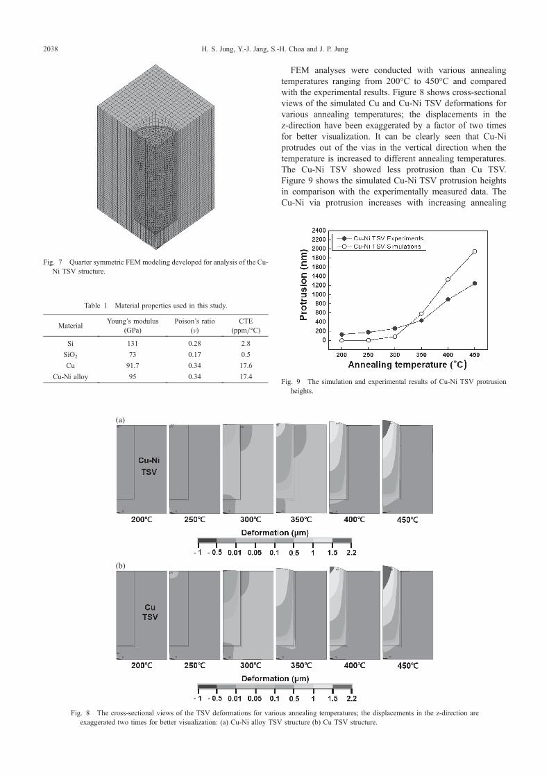
FEM analyses were conducted with various annealingtemperatures ranging from 200°C to 450°C and comparedwith the experimental results. Figure 8 shows cross-sectionalviews of the simulated Cu and Cu-Ni TSV deformations forvarious annealing temperatures; the displacements in thez-direction have been exaggerated by a factor of two timesfor better visualization. It can be clearly seen that Cu-Niprotrudes out of the vias in the vertical direction when thetemperature is increased to different annealing temperatures.The Cu-Ni TSV showed less protrusion than Cu TSV.Figure 9 shows the simulated Cu-Ni TSV protrusion heightsin comparison with the experimentally measured data. TheCu-Ni via protrusion increases with increasing annealing
Table 1 Material properties used in this study.
MaterialYoung’s modulus
(GPa)Poison’s ratio
(¯)CTE
(ppm/°C)
Si 131 0.28 2.8
SiO2 73 0.17 0.5
Cu 91.7 0.34 17.6
Cu-Ni alloy 95 0.34 17.4
Fig. 7 Quarter symmetric FEM modeling developed for analysis of the Cu-Ni TSV structure.
(a)
(b)
Fig. 8 The cross-sectional views of the TSV deformations for various annealing temperatures; the displacements in the z-direction areexaggerated two times for better visualization: (a) Cu-Ni alloy TSV structure (b) Cu TSV structure.
Fig. 9 The simulation and experimental results of Cu-Ni TSV protrusionheights.
H. S. Jung, Y.-J. Jang, S.-H. Choa and J. P. Jung2038
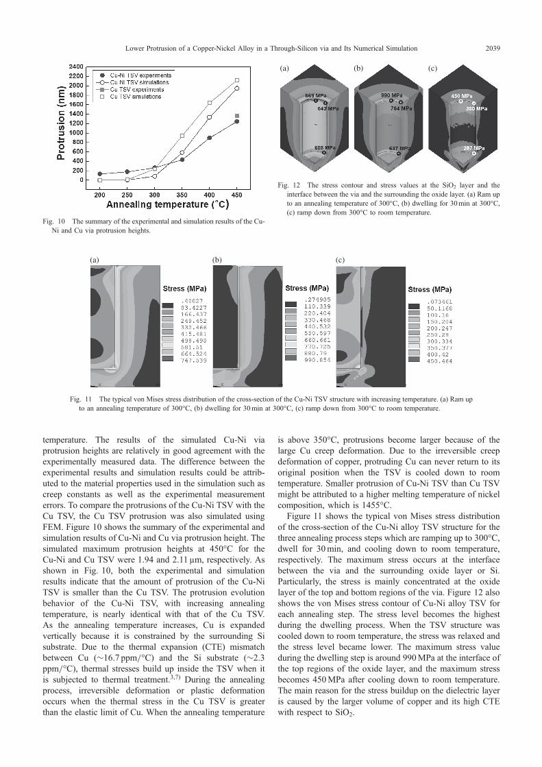
temperature. The results of the simulated Cu-Ni viaprotrusion heights are relatively in good agreement with theexperimentally measured data. The difference between theexperimental results and simulation results could be attrib-uted to the material properties used in the simulation such ascreep constants as well as the experimental measurementerrors. To compare the protrusions of the Cu-Ni TSV with theCu TSV, the Cu TSV protrusion was also simulated usingFEM. Figure 10 shows the summary of the experimental andsimulation results of Cu-Ni and Cu via protrusion height. Thesimulated maximum protrusion heights at 450°C for theCu-Ni and Cu TSV were 1.94 and 2.11 µm, respectively. Asshown in Fig. 10, both the experimental and simulationresults indicate that the amount of protrusion of the Cu-NiTSV is smaller than the Cu TSV. The protrusion evolutionbehavior of the Cu-Ni TSV, with increasing annealingtemperature, is nearly identical with that of the Cu TSV.As the annealing temperature increases, Cu is expandedvertically because it is constrained by the surrounding Sisubstrate. Due to the thermal expansion (CTE) mismatchbetween Cu (³16.7 ppm/°C) and the Si substrate (³2.3ppm/°C), thermal stresses build up inside the TSV when itis subjected to thermal treatment.3,7) During the annealingprocess, irreversible deformation or plastic deformationoccurs when the thermal stress in the Cu TSV is greaterthan the elastic limit of Cu. When the annealing temperature
is above 350°C, protrusions become larger because of thelarge Cu creep deformation. Due to the irreversible creepdeformation of copper, protruding Cu can never return to itsoriginal position when the TSV is cooled down to roomtemperature. Smaller protrusion of Cu-Ni TSV than Cu TSVmight be attributed to a higher melting temperature of nickelcomposition, which is 1455°C.
Figure 11 shows the typical von Mises stress distributionof the cross-section of the Cu-Ni alloy TSV structure for thethree annealing process steps which are ramping up to 300°C,dwell for 30min, and cooling down to room temperature,respectively. The maximum stress occurs at the interfacebetween the via and the surrounding oxide layer or Si.Particularly, the stress is mainly concentrated at the oxidelayer of the top and bottom regions of the via. Figure 12 alsoshows the von Mises stress contour of Cu-Ni alloy TSV foreach annealing step. The stress level becomes the highestduring the dwelling process. When the TSV structure wascooled down to room temperature, the stress was relaxed andthe stress level became lower. The maximum stress valueduring the dwelling step is around 990MPa at the interface ofthe top regions of the oxide layer, and the maximum stressbecomes 450MPa after cooling down to room temperature.The main reason for the stress buildup on the dielectric layeris caused by the larger volume of copper and its high CTEwith respect to SiO2.
Fig. 10 The summary of the experimental and simulation results of the Cu-Ni and Cu via protrusion heights.
(a) (b) (c)
Fig. 11 The typical von Mises stress distribution of the cross-section of the Cu-Ni TSV structure with increasing temperature. (a) Ram upto an annealing temperature of 300°C, (b) dwelling for 30min at 300°C, (c) ramp down from 300°C to room temperature.
(a) (b) (c)
Fig. 12 The stress contour and stress values at the SiO2 layer and theinterface between the via and the surrounding the oxide layer. (a) Ram upto an annealing temperature of 300°C, (b) dwelling for 30min at 300°C,(c) ramp down from 300°C to room temperature.
Lower Protrusion of a Copper-Nickel Alloy in a Through-Silicon via and Its Numerical Simulation 2039

Figure 13 shows the simulation results of the maximumvon Mises stress in the Cu-Ni via and the Cu via after coolingdown to room temperature with increasing annealing temper-ature. The maximum stress increases with increasingannealing temperature. In particular, the maximum stressincreases sharply at a temperature of 300°C possibly owingto the creep effect of via material. Higher annealingtemperature generates larger creep deformation of Cu-Niand Cu TSV via, which is irreversible deformation and thusresults in larger stress when temperature changes fromannealing temperature to room temperature. At a higherannealing temperature, the stress increased slightly due to thesoftening effect of the Cu and Cu-Ni via material. In general,the Cu-Ni via exhibited lower stress level than the Cu viastructure, however, the differences in stress level becomesmall from 350°C. At an annealing temperature of 300°C, themaximum stress in the Cu-Ni and Cu via is around 460 and519MPa, respectively. This thermal stress is high enough tocause plastic deformation of the Cu-Ni and Cu, and the viaextrusion may remain even after cooling. Figure 14 revealsthe maximum von Mises stress subjected to the silicon waferwith increasing annealing temperature. The maximum stresson the silicon wafer showed similar trend with the maximumstress on the via. The maximum stress increases withincreasing annealing temperature due to an increase in thethermal expansion mismatch with the via. The maximum
stress of Cu-Ni TSVand Cu TSVat an annealing temperatureof 450°C is 1.08GPa and 1.12GPa, respectively. The Cu-NiTSV showed a slightly lower stress value than the Cu TSV.
4. Conclusion
In this study, we investigated the characteristics of Cu-Nialloy via protrusions at various annealing temperatures. Highspeed Cu-Ni alloy filling into vias was performed with theelectroplating process using a periodic pulse reverse currentwaveform. The filled Cu-Ni TSVs revealed a 100% fillingratio without defects and consisted of 92mass% Cu and8mass% Ni. Protrusions of the Cu-Ni vias at variousannealing temperatures were investigated with experimentaland numerical analyses and compared with Cu vias. Thesize of the protrusions gradually increased with annealingtemperature and started to increase substantially at 350°C.The Cu-Ni TSV showed lower via protrusion relative to theCu TSV. The simulated Cu-Ni via protrusion heights wererelatively well-matched with the experimentally measureddata. The simulation results also showed that the Cu-Ni TSVsshowed smaller protrusions than the Cu TSVs. As theannealing temperature increased, the Cu-Ni via expandedvertically due to the CTE mismatch between the via and thesurrounding materials. When the temperature increased toabove 350°C, protrusions became larger due to increased Cucreep deformation. The von Mises stress in the Cu-Ni viaincreased with increasing annealing temperature, and increas-ed substantially at a temperature of 300°C due to the creepeffect of via material. Overall, the Cu-Ni alloy TSV showedhigh speed filling and a lower via protrusion. This indicatesthat Cu-Ni alloy vias represent a promising alternative to Cuvias for TSV technologies.
Acknowledgments
This work was supported by a grant from the IndustrialCore Technology Development Program of “Development ofinductor and power devices using thick Cu plate with 20 µmthickness (10048344)” and “Development of thermo-com-pression joining technology with speed of 6 sec/chip andpitch size of 20 µm (10051605)” funded by the Ministry ofTrade, Industry & Energy, Republic of Korea.
REFERENCES
1) T. Kobayashi, J. Kawasaki, K. Miura and H. Honma: Electrochim. Acta47 (2001) 8589.
2) M. Lefebvre, G. Allardyce, M. Seita, H. Tsuchida, M. Kusaka and S.Hayashi: Circuit World 29 (2003) 914.
3) N. Ranganathan, K. Prasad, N. Balasubramanian and K. L. Pey:J. Micromech. Microeng. 18 (2008) 075018.
4) E. J. Cheng and Y. L. Shen: Microelectron. Reliab. 52 (2012) 534540.5) I. De Wolf, K. Croes, O. V. Pedreira, R. Labie, A. Redolfi and M. V.
Peer: Microelectron. Reliab. 51 (2011) 18561859.6) L. W. Kong, A. C. Rudack, P. Krueger, E. Zschech, S. Arkalgud and
A. C. Diebold: Microelectron. Eng. 92 (2012) 2428.7) F. X. Che, W. N. Putra, A. Heryanto and A. Trigg: IEEE Trans.
Compon. Packag. Manuf. Technol. 3 (2013) 732739.8) T. Jiang, S. K. Ryu, Q. Zhao, J. Im, R. Huang and S. Paul Ho:
Microelectron. Reliab. 53 (2013) 5362.9) A. Heryanto, W. N. Putra, A. D. Trigg, S. Gao, W. S. Kwon, F. X. Che,
X. F. Ang, J. Wei, R. I. Made and C. L. Gan: J. Electron. Mater. 41
Fig. 13 Maximum von Mises stress of the TSV vias with increasingannealing temperature.
Fig. 14 Maximum von Mises stress of the silicon wafer with increasingannealing temperature.
H. S. Jung, Y.-J. Jang, S.-H. Choa and J. P. Jung2040

(2012) 25332542.10) C. Lee, S. Tsuru, Y. Kanda, S. Ikeda and M. Matsumura:
J. Electrochem. Soc. 156 (2009) D543D547.11) K. Y. K. Tsui, S. K. Yau, V. C. K. Leung, P. Sun and D. X. Q. Shi: Proc.
Int. Conf. on Electron. Pack. Tech. & High Dens. Pack. (ICEPT-HDP),(2009) pp. 2327.
12) J. S. Bae, G. H. Chang and J. H. Lee: J. Microelectron. Pack. Soc. 12(2005) 129134.
13) A. Pohjoranta and R. Tenno: J. Electrochem. Soc. 154 (2007) D502D509.
14) T. Dao, D. H. Triyoso, R. Mora, T. Kropewnicki, B. Griesbach, D.Booker, M. Petras and V. Adams: Proc. Int. Symp. on VLSI Des. Aut.Test (VLSI-DAT), (2010) pp. 710.
15) Q. Chen, C. Huang and Z. Wang: Microelectron. Reliab. 52 (2012)26702676.
16) A. Tsukada, R. Sato, S. Sekine, R. Kimura, K. Kishi, Y. Sato, Y. Iwataand H. Murata: Proc. 61st IEEE Electron. Comp. Tech. Conf. (ECTC),
(2011) pp. 19811986.17) Y. Jee, J. Yu, K. Park and T. Oh: J. Electron. Mater. 38 (2009) 685690.18) R. He, H. Wang, J. Zhou, X. Guo, D. Yu and L. Wan: Proc. Int. Conf.
on Electron. Pack. Tech. & High Dens. Pack. (ICEPT-HDP), (2011)pp. 14.
19) Y. K. Ko, H. T. Fujii, Y. S. Sato, C. W. Lee and S. Yoo: Microelectron.Eng. 89 (2012) 6264.
20) S. C. Hong, S. Kumar, D. H. Jung, W. J. Kim and J. P. Jung: Met.Mater. Int. 19 (2013) 123128.
21) M. Gad-el-Hak: The MEMS Handbook, 2nd Ed., (CRC Press, 2002)p. 35.
22) G. R. Blackwell: The Electronic Packaging Handbook, (CRC PressLLC, Florida, 2000) p. 521.
23) S. Park, H. C. Lee, B. Sammakia and K. Raghunathan: IEEE Trans.Compon. Packag. Technol. 30 (2007) 294301.
24) G. Li, B. G. Thomas and J. F. Stubbins: Metall. Mater. Trans. A 31(2000) 24912502.
Lower Protrusion of a Copper-Nickel Alloy in a Through-Silicon via and Its Numerical Simulation 2041