low-temperature crystallization of sol gel-derived lead …hf5/paper/material/2007 thin solid...
TRANSCRIPT

007) 2891–2896www.elsevier.com/locate/tsf
Thin Solid Films 515 (2
Low-temperature crystallization of sol–gel-derived lead zirconate titanatethin films using 2.45 GHz microwaves
Ankam Bhaskar a,⁎, T.H. Chang a, H.Y. Chang b, S.Y. Cheng c
a Department of Physics, National Tsing Hua University, Hsinchu, Taiwanb Department of Marine Engineering, National Taiwan Ocean University, Keelung, Taiwan
c Material and Chemical Research Laboratories, Industrial Technology Research Institute, Chutung 31060, Hsinchu, Taiwan
Received 4 April 2006; received in revised form 31 July 2006; accepted 28 August 2006Available online 11 October 2006
Abstract
Lead zirconate titanate (PZT) thin films of thickness 420 nm were deposited on Pt/Ti/SiO2/Si substrate using a spin coating sol–gel precursorsolution, and then annealed using 2.45 GHz microwaves at a temperature of 450 °C for 30 min. The film has a high perovskite content and highcrystallinity with a full width at half maximum of 0.35°. The surface roughness of the PZT thin film was 1.63 nm. Well-saturated ferroelectricproperties were obtained with a remanent polarization of 46.86 μC/cm2 and coercive field of 86.25 kV/cm. The film also exhibited excellentdielectric properties with a dielectric constant of 1140 and a dissipation factor of 0.03. These properties are superior to those obtained byconventional annealing at a temperature of 700 °C for 30 min.© 2006 Elsevier B.V. All rights reserved.
Keywords: Microwave annealing; Surface roughness; Dielectric properties; Hysteresis loops; Lead zirconate titanate
1. Introduction
Thin films of ferroelectric materials can be used in a varietyof applications in the microelectronics industry, for examplenon-volatile memories, high-frequency capacitor applications,pyroelectric detectors, sensors, actuators, and transducers. Oneof the most useful materials for thin films is Pb (ZrxTi1−x) O3
(PZT), because it has excellent piezoelectric, pyroelectric, anddielectric properties. The formation of the ferroelectricperovskite phase in PZT thin films generally occurs above600 °C. These high temperatures often cause problems of PZTdiffusion between layers, and make the PZT thin filmsunsuitable for high-density devices [1]. Therefore, reducingthe processing temperature for the ferroelectric thin films hasbeen the goal of researchers. Many groups are attempting toprepare PZT thin films at low-temperatures by varioustechniques such as electrophoretic deposition [2], hydrothermalsynthesis [3], radio frequency (rf) sputtering [4], sol–gelprocess [5], CO2 laser annealing [6], metal-organic chemicalvapor deposition [7], and millimeter wave annealing [8].
⁎ Corresponding author. Tel.: +886 3 574 2560x13; fax: +886 3 572 3052.E-mail address: [email protected] (A. Bhaskar).
0040-6090/$ - see front matter © 2006 Elsevier B.V. All rights reserved.doi:10.1016/j.tsf.2006.08.044
Microwave processing of ceramics has attracted considerableattention in recent years [9,10]. The advantages of microwaveheating over conventional heating are that the heat is generateduniformly throughout the material, resulting in a uniform sin-tering of the material, lower required sintering temperature andtime, a suppression of grain growth, and very rapid heating rates[11]. Microwaves have been utilized for both the synthesis and inthe sintering of a wide variety of materials, especially oxides[12,13]. Microwave processing has been adopted to anneal films[14,15]. Song et al. [15], using a multimode cavity of 2.45 GHzmicrowaves, completed the formation of perovskite-phase PZTthin films at a lower temperature (600 °C) than that of con-ventionally annealed PZT thin films (700 °C). However, low-temperature processing (b500 °C) of PZT thin films using2.45 GHz microwaves has not been reported.
This study reports the low-temperature processing of PZT thinfilms deposited on Pt/Ti/SiO2/Si substrate using a single-modecavity of 2.45 GHz microwaves, to obtain good dielectric, andferroelectric properties. The crystal structure, the surfacemorpho-logy, and the electrical properties of PZT thin films were inves-tigated. Based on experimental results, the effect of 2.45 GHzmicrowaves on PZT thin films is discussed; and compared to theeffect of conventional annealing of PZT thin films.

Fig. 1. Comparison of time–temperature profiles of conventionally (C.A) andmicrowave (M.A) annealed PZT thin films.
2892 A. Bhaskar et al. / Thin Solid Films 515 (2007) 2891–2896
2. Experiment
PZT thin films were prepared by the sol–gel method. The leadacetate trihydrate was dissolved in 2-methoxyethanol; thesolutions were heated to 110 °C, and then refluxed for 2 h.The solutions were cooled to 90 °C before the required quantitiesof zirconium-n-propoxide and 2-methoxyethanol were addedsequentially and refluxed for 1 h. Isopropyl-orthotitanate wasadded to the same as zirconium-n-propoxide processing for 2 h.Clear light yellow PZTstock was obtained by air-cooling to roomtemperature. The solution was stable and no crystallite formed forseveral months. The concentration of the final solution can beadjusted to 0.2 M by adding or distilling an appropriate quantityof solvent. The precursor solution was entirely prepared in anambient atmosphere. The nominal composition of the solutionwas Pb: Zr: Ti=1.1: 0.53: 0.47. Pt/Ti/SiO2/Si substrates, whichprovide nucleation sites for the perovskite phase because of goodlattice matching, were selected [16]. The precursor solution wasdeposited on Pt/Ti/SiO2/Si substrates by spin coating at 500 rpmfor 1 s and at 3000 rpm for 15 s. The as-deposited layer was driedon a hot plate in air at 150 °C for 5 min and decomposed at400 °C for 10 min to evaporate alcohol and organics. Thedecomposition temperature was established by the thermogravimetric analysis, which indicates that at 400 °C, most ofthe organics evaporated and decomposed from the PZT thinfilms. The spin coating and drying process were repeated tentimes, to obtain the desired thickness of 420 nm.
The PZT thin film was placed in a casket, which wasthermally insulated. The casket was located at the center of thehighest electric field in the applicator. SiC rods are used assusceptors because PZT does not absorb 2.45 GHz microwavesat room temperature [17]. The microwave energy initially heatedthe SiC rods, which, in turn, transferred heat to the insulationand eventually to the thin film [18]. As the temperature of thePZT thin film increased, it more effectively coupled with themicrowave energy, promoting direct heating. The microwavefrequency was 2.45 GHz and the power was adjusted 350±50 W, to a maintained annealing temperature of 450 °C. Thetemperature was controlled to within ±1 °C by continuouslyadjusting. The temperature was measured using a thermocouple(Pt and 87%Pt–13%Rh) with an alumina sheath, which was incontact with the surface of film. The PZT thin films wereannealed by 2.45 GHz microwaves at 450 °C for 30 min, and theconventionally annealed at 700° for 30 min.
Fig. 1 compares the time–temperature profile of theconventional annealing and the microwave annealing of PZTthin films. The microwave annealing was conducted at 450 °Cfor 30 min with an average ramp rate of 25 °C/min. The totalcycle time was 48 min, excluding the period of cooling. Forcomparison, conventional annealing was also conducted at700 °C for 30 min with an average ramp rate of 5 °C/min.Cooling at 5 °C/min to 300 °C was followed by natural cooling.Excluding the cooling period, it took about 2 h 45 min, whichwas much longer (1 h 55 min) than the microwave annealingtime (50 min). The advantage of processing temperature, energy,and time efficiency of microwave annealing over conventionalannealing is unambiguously shown.
The crystalline structures of the PZT thin films wereexamined by X-ray diffraction (XRD) (Rigaku D/MAX-IIB,Cu Kα radiation wavelength λ=1.5405 Å, scan speed of2° per min.). The film thickness, surface morphologies, andcross-sections of the PZT thin films were examined under fieldemission scanning electron microscope (FE-SEM) (JSM-6500F). The surface roughness of PZT thin films was char-acterized using a Seiko Instruments (Inc. SPI3800N) atomicforce microscope (AFM) system. Au electrodes were depos-ited by rf sputtering on the top surface of PZT thin filmsthrough a shadow mask with a diameter of 1 mm for electricalmeasurements. This deposition was conducted at roomtemperature. The dielectric properties were measured atroom temperature in the frequency range 1 kHz to 1 MHzusing an impedance analyzer (HP impedance/gain analyzer4194A). The polarization-electric (P-E) hysteresis loops weremeasured using a Radiant Technologies RT-66A ferroelectrictest system by applying triangular voltages at a frequency of1 kHz.
3. Results and discussion
Fig. 2a shows that the conventional annealing of PZT thinfilms at 450 °C yields a broad diffraction peak of (2 2 2) planesof the pyrochlore phase. No peak of the perovskite phase wasdetected in the thin film because the temperature of the PZTthin film was not high enough for the reaction to occur amongthe Pb, Ti, Zr, and O. The microwave-annealed PZT thin film(450 °C) yields a prominent diffraction peak of the perovskitephase (1 1 0) planes, and no peak of the pyrochlore phase wasdetected in this film. The conventionally annealed PZT thinfilm at 700 °C yielded an XRD pattern that was similar to thatof the PZT thin film annealed using 2.45 GHz microwaves.The peak with the highest intensity in the X-ray diffractionpattern of the PZT thin film was indexed as (1 1 0) planes,indicating that the thin film was mostly randomly oriented.The full width at half maximum (FWHM) of the perovskitephase peak (1 1 0) was considered in evaluating the quality ofthe PZT thin film. In all of the XRD patterns (Fig. 2a), a peakat around 2θ=30.6–31.8° was observed, corresponding to the

Fig. 2. (a) XRD patterns of PZT thin films annealed by microwave annealing(M.A), and conventional annealing (C.A) (b) The peak at 2θ=30.6–31.8° in theXRD pattern (Fig. 1a) redrawn on an expanded scale to emphasize the intensityand FWHM of the perovskite phase peak (1 1 0).
Fig. 3. FE-SEM image of PZT thin films annealed by microwaves (a) andconventionally (b).
2893A. Bhaskar et al. / Thin Solid Films 515 (2007) 2891–2896
(1 1 0) perovskite plane. This peak was redrawn on anexpanded scale in Fig. 2b. The conventionally annealed PZTthin film at 450 °C does not yield any peak. The microwave-annealed PZT thin film (450 °C) yielded a higher (1 1 0)perovskite phase peak, whose FWHM (0.35°) was narrowerthan that of the FWHM (0.43°) of the conventionally annealedPZT thin film at 700 °C. The microwave-annealed PZT thin
film (450 °C) exhibits better crystallinity and higher thin filmquality than that of the conventionally annealed PZT thin filmat 700 °C. The processing temperature of the microwaveannealing was much lower (250 °C) than that of the con-ventional annealing. Similar trends have also been reportedfor the micro/millimeter wave processing of ferroelectric thinfilms. Song et al. [15] formed a PZT thin film containing only aperovskite phase using a multimode cavity of 2.45 GHzmicrowaves at a lower temperature (600°C) than used in theconventional annealing of PZT thin films (700 °C). The pre-sently reporting microwave-annealed PZT thin film is 150 °Clower than above reported value, perhaps because the cavitywas single-mode or the mode of precursor method. Themultimode cavity of 2.45 GHz microwaves has a criticaldrawback since the electromagnetic field in the cavity was notuniform; resulting in inhomogeneous heating and the un-avoidable formation of hot spots [9]. Wang et al. [8] reportedthe PZT thin film crystallization at 480 °C using 28 GHzmicrowave irradiation, at a temperature 120 °C lower than theconventionally annealed PZT thin film (600 °C). Mastsumotoet al. [19] conducted research on the mm-wave (28 GHz)processing of SrTiO3 thin films and compared the results withthose of conventional processing; they have reported that themillimeter wave processing reduced the annealing temperatureby more than 90 °C, probably because mm-wave irradiationenhances the diffusion of atoms. Many researchers in the fieldof sintering have reported that ceramics were densified at

Fig. 4. AFM two-dimensional images of PZT thin films annealed bymicrowaves (a) and conventionally (b).
Fig. 5. FE-SEM cross-sectional image of PZT thin films annealed bymicrowaves (a) and conventionally (b).
2894 A. Bhaskar et al. / Thin Solid Films 515 (2007) 2891–2896
lower temperature by the microwave heating due to theenhanced diffusion [20,21].
The surface morphologies of PZT thin films were examinedby FE-SEM. The microwave annealing of PZT thin film(450 °C) yields dense and fine grains, uniform and withoutcracks, with an average grains size of (∼27 nm) (Fig. 3a). Theconventional annealing of PZT thin film yields both large andsmall grains, which were not uniform, and had an average grainsize of ∼90 nm (Fig. 3b). The conventionally annealed of PZTthin film at 700 °C has larger grains than the microwave-annealed PZT thin film, perhaps because of the differencebetween the rise ramp rates of the annealing temperatures, asindicated in Fig. 1. The Laser-Induced Phase transformationTechnique (LIPT) of PZT thin films yielded similar trendresults. Lu et al. [22] reported that the grain sizes of PZT thin
films with LIPT were much smaller than those of the filmsannealed in an oven. They attributed this result to thedifference between the slow rate of rise of temperature inoven annealing and fast rate of rise associated with the LIPTprocess.
The surface roughness was examined by AFM. Fig. 4 showsthe two-dimensional image of PZT thin films that were annealedby microwaves and conventionally. The microwave annealingof PZT thin film yields small grains, which are more uniformlydistributed than those in the conventionally annealed PZT thinfilm. The microwave-annealed PZT thin film had a smoothersurface, with a root mean square (rms) roughness of 1.63 nm,than the conventionally annealed PZT thin film, which had anrms roughness of 5.11 nm. The roughening was interpreted as aresult of grain agglomeration and enlargement of grains. Theuniformity of the PZT thin film was improved with microwaveannealing because with shorter sintering cycles and reducedthermal gradients, finer grains were obtained and the grainswere more uniformly sized.
Fig. 5 shows the cross-sectional FESEM image of micro-wave-annealed and conventionally annealed PZT thin filmmultilayer (PZT, Pt, Ti, SiO2, Si) structures, as well as theinterface between the PZT film and the bottom electrode (Pt).The thickness of the PZT thin films was 420 nm. Themicrowave annealing of PZT films yields a clear interfacebetween the film and the bottom electrode. The conventionalannealing of PZT thin films yields the same interface as the
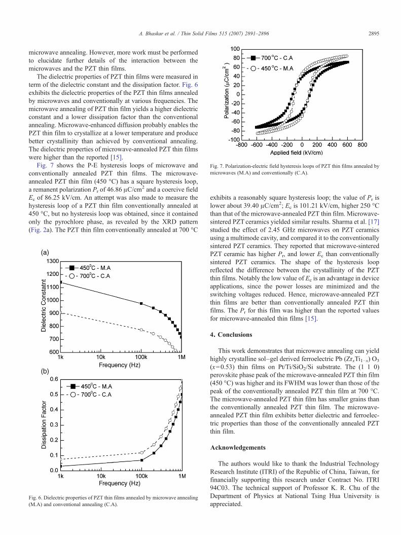
Fig. 7. Polarization-electric field hysteresis loops of PZT thin films annealed bymicrowaves (M.A) and conventionally (C.A).
2895A. Bhaskar et al. / Thin Solid Films 515 (2007) 2891–2896
microwave annealing. However, more work must be performedto elucidate further details of the interaction between themicrowaves and the PZT thin films.
The dielectric properties of PZT thin films were measured interm of the dielectric constant and the dissipation factor. Fig. 6exhibits the dielectric properties of the PZT thin films annealedby microwaves and conventionally at various frequencies. Themicrowave annealing of PZT thin film yields a higher dielectricconstant and a lower dissipation factor than the conventionalannealing. Microwave-enhanced diffusion probably enables thePZT thin film to crystallize at a lower temperature and producebetter crystallinity than achieved by conventional annealing.The dielectric properties of microwave-annealed PZT thin filmswere higher than the reported [15].
Fig. 7 shows the P-E hysteresis loops of microwave andconventionally annealed PZT thin films. The microwave-annealed PZT thin film (450 °C) has a square hysteresis loop,a remanent polarization Pr of 46.86 μC/cm
2 and a coercive fieldEc of 86.25 kV/cm. An attempt was also made to measure thehysteresis loop of a PZT thin film conventionally annealed at450 °C, but no hysteresis loop was obtained, since it containedonly the pyrochlore phase, as revealed by the XRD pattern(Fig. 2a). The PZT thin film conventionally annealed at 700 °C
Fig. 6. Dielectric properties of PZT thin films annealed by microwave annealing(M.A) and conventional annealing (C.A).
exhibits a reasonably square hysteresis loop; the value of Pr islower about 39.40 μC/cm2; Ec is 101.21 kV/cm, higher 250 °Cthan that of the microwave-annealed PZT thin film. Microwave-sintered PZT ceramics yielded similar results. Sharma et al. [17]studied the effect of 2.45 GHz microwaves on PZT ceramicsusing a multimode cavity, and compared it to the conventionallysintered PZT ceramics. They reported that microwave-sinteredPZT ceramic has higher Pr, and lower Ec than conventionallysintered PZT ceramics. The shape of the hysteresis loopreflected the difference between the crystallinity of the PZTthin films. Notably the low value of Ec is an advantage in deviceapplications, since the power losses are minimized and theswitching voltages reduced. Hence, microwave-annealed PZTthin films are better than conventionally annealed PZT thinfilms. The Pr for this film was higher than the reported valuesfor microwave-annealed thin films [15].
4. Conclusions
This work demonstrates that microwave annealing can yieldhighly crystalline sol–gel derived ferroelectric Pb (ZrxTi1−x) O3
(x=0.53) thin films on Pt/Ti/SiO2/Si substrate. The (1 1 0)perovskite phase peak of the microwave-annealed PZT thin film(450 °C) was higher and its FWHM was lower than those of thepeak of the conventionally annealed PZT thin film at 700 °C.The microwave-annealed PZT thin film has smaller grains thanthe conventionally annealed PZT thin film. The microwave-annealed PZT thin film exhibits better dielectric and ferroelec-tric properties than those of the conventionally annealed PZTthin film.
Acknowledgements
The authors would like to thank the Industrial TechnologyResearch Institute (ITRI) of the Republic of China, Taiwan, forfinancially supporting this research under Contract No. ITRI94C03. The technical support of Professor K. R. Chu of theDepartment of Physics at National Tsing Hua University isappreciated.

2896 A. Bhaskar et al. / Thin Solid Films 515 (2007) 2891–2896
References
[1] T.M. Shaw, S. Trolier-Mckinstry, P.C. McIntyre, Annu. Rev. Mater. Sci. 30(2000) 263.
[2] S. Sugiyama, A. Takagi, K. Tsuzuki, Jpn. J. Appl. Phys. 30 (1991) 2170.[3] K. Shimomura, T. Tsurumi, Y. Ohba, M. Daimon, Jpn. J. Appl. Phys. 30
(1991) 2174.[4] S. Watanabe, T. Fujiu, T. Fujii, Appl. Phys. Lett. 66 (1995) 1481.[5] Y.J. Song, Y. Zhu, S.B. Desu, Appl. Phys. Lett. 72 (1998) 2686.[6] H.C. Pan, C.C. Chou, H.L. Tsai, Appl. Phys. Lett. 83 (2003) 3156.[7] A. Nagai, H. Morioka, G. Asano, H. Funakubo, A. Saiki, Appl. Phys. Lett.
86 (2005) 142906.[8] Z.J. Wang, H. Kokawa, H. Takizawa, M. Ichiki, R. Maeda, Appl. Phys.
Lett. 86 (2005) 212903.[9] W.H. Sutton, Am. Ceram. Soc. Bull. 68 (1989) 376.[10] R. Roy, D. Agrawal, J. Cheng, S. Gedevanishvili, Nature 399 (1999) 668.[11] D.K. Agrawal, Curr. Opin. Solid State Mater. Sci. 3 (1998) 480.[12] P.D. Ramesh, D. Brandon, L. Schachter, Mater. Sci. Eng. A266 (1999) 211.
[13] J. Cheng, D.K. Agarwal, S. Komarneni, M. Mathis, R. Roy, Mater. Res.Innov. 1 (1997) 44.
[14] J.N. Hart, Y.-B. Cheng, G.P. Simon, L. Spiccia, Surf. Coat. Technol. 198(2005) 20.
[15] S. Song, X. Fu, H. Tan, M. Tao, L. Chen, L. Wang, C. Lin, Phys. StatusSolidi A 164 (1997) 779.
[16] T. Tani, Z. Xu, D.A. Payne, Mater. Res. Soc. Symp. Proc. 310 (1993) 269.[17] P.K Sharma, Z. Ounaies, V.V. Vardan, V.K. Varadan, Smart Mater. Struct.
10 (2001) 878.[18] N.S.L.S. Vasconcelos, J.S. Vasconcelos, V. Bouquet, S.M. Zanetti, E.R.
Leite, E. Longo, L.E.B. Soledade, F.M. Pontes, M. Guilloux-Viry, A.Perrin, M.I. Bernardi, J.A. Varela, Thin Solid Films 436 (2003) 213.
[19] T. Matsumoto, A. Niino, S. Baba, K. Numata, S. Miyake, Surf. Coat.Technol. 174–175 (2003) 611.
[20] R. Wroe, A.T. Rowley, J. Mater. Sci. 31 (1996) 2019.[21] S.J. Rothman, Mater. Res. Soc. Symp. Proc. 9 (1994) 347.[22] X.M. Lu, J.S. Zhu, X.F. Huang, C.Y. Lin, Y.N. Wang, Appl. Phys. Lett. 65
(1994) 2015.