low power radio circuitsrfic.eecs.berkeley.edu/~niknejad/ee142_fa05lects/pdf/...low power radio...
TRANSCRIPT

Low power Radio Circuits
EE 142 Guest LectureAlyosha Molnar

Overview: Smart Dust Radio
• Performance:– range ≤10m– data rate: ~100kb/s – <1% duty cycle– Battery life ~5yrs
• Low power:1mW– Stack circuits to
reuse current– Drive RF gates from
high-Q LC oscillator
• Cost: <$1, so few off-chip components:– Battery (3V Li coin cell)– Crystal (for network
sync)– Antenna– High-Q inductor– 0.25µm
Goal: A radio for sensor nodes which contain:sensors, ADC, µP and ~1kB RAM

VDD = 2.7-3.6V
-
+FSK
Demod
bitscounter
FLL bitsN
Div 8
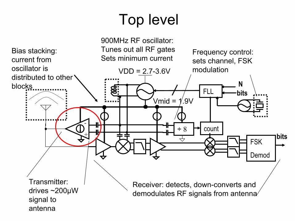
900MHz RF oscillator: Tunes out all RF gatesSets minimum current
Top level
Bias stacking: current from oscillator is distributed to other blocks
Vmid = 1.9V
Frequency control: sets channel, FSK modulation
FLL
÷ 8 count-
+
Transmitter: drives ~200µW signal to antenna
FSK
Demod
Receiver: detects, down-converts and demodulates RF signals from antenna

Oscillator
• Cross-coupled inverters form a negative resistance.
• Tuning: – 902MHz-928MHz– ± 5% for process– ± 2.5% for inductor
• L = 17nH, Q = 30• Swing = 1Vpeak• Ibias = 200-300µA
VDD
I bia
s
VCOVSS
gm
gm

Simulations (unloaded)
Output Spectrum Phase noise
Transient output Tail voltage (with IC)
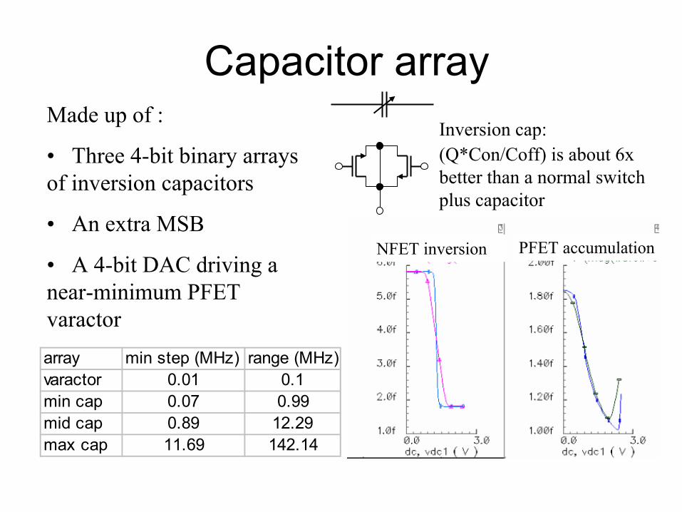
Capacitor arrayInversion cap:(Q*Con/Coff) is about 6x better than a normal switch plus capacitor
array min step (MHz) range (MHz)varactor 0.01 0.1min cap 0.07 0.99mid cap 0.89 12.29max cap 11.69 142.14
NFET inversion PFET accumulation
Made up of :
• Three 4-bit binary arrays of inversion capacitors
• An extra MSB
• A 4-bit DAC driving a near-minimum PFET varactor

Oscillator results
• Tuning from 820MHz to 960MHz
• LSB precision of 2.6 kHz• Phase noise @ 1MHz = -
107dBc• PN rolls off @ 40dB/dec
below 1MHz, 20dB/dec above.
• Noise is bias dominated.• Oscillator starts to squegg for
Ibias below 200µA (220µW)
Tuning range
800820840860880900920940960980
0 10 20 30
MSB setting
F, M
Hz

VDD = 2.7-3.6V
-
+FSK
Demod
bitscounter
FLL bitsN
Div 8
900MHz RF oscillator: Tunes out all RF gatesSets minimum current
Top level
Bias stacking: current from oscillator is distributed to other blocks
Vmid = 1.9V
Frequency control: sets channel, FSK modulation
FLL
÷ 8 count-
+
Transmitter: drives ~200µW signal to antenna
FSK
Demod
Receiver: detects, down-converts and demodulates RF signals from antenna

Frequency control loop (FLL)
• Have Crystal oscillator for network synchrony.• RF Oscillator control is digital.
– Crystal samples continuously running counter.– Subtracting successive samples gives FRF/Fref.
• Early counter stages set power, so– Use some custom logic.– divide-by-8 before counter
Modulo 65536 counter
Latch
Div 8
Accumulator
Latch
+-ΣΣ
N
Ref+-Σ
MOD

Divider designVDD
Vmid
D Q D Q D Q D Q
+
-
D QD QD Q

Ring Divider Simulation• Four stages with
~1ns delay set by input.
• Extra inverter incorporating reset capability.
• Fails by dividing by 9 (extra inverter causes cyclic slip).
Q4
Q3
Q2
Q1
Q4
osc

Divider/FLL results
• FLL works– Accurately sets
frequency– Stabilizes Frequency
under bias perturbations
• Divider fails at low currents by under counting.
• Requires ~ 55µW
30000
32000
34000
36000
38000
40000
27 32 37 42
Idiv, uA
divi
de ra
tio
911MHz
956MHz
827MHz
VDD = 2.7-3.6V
-
+FSK
Demod
bitscounter
FLL bitsN
Div 8
900MHz RF oscillator: Tunes out all RF gatesSets minimum current
Top level
Bias stacking: current from oscillator is distributed to other blocks
Vmid = 1.9V
Frequency control: sets channel, FSK modulation
FLL
÷ 8 count-
+
Transmitter: drives ~200µW signal to antenna
FSK
Demod
Receiver: detects, down-converts and demodulates RF signals from antenna

Transmitter• Transmitter is just a buffering of the oscillator.• Want to transmit 100-300uW• Simple antennas have impedance of ~100 ohms.• For low cost, impedance matching is limited to a
series inductor (can be part of the antenna).• This implies the driver must source a 1mA, 200mV
rms signal from a 3V supply: this will be inefficient!• So stack two amplifiers and reuse bias.

Transmitter designVDD
I bias
Vmid
Ibias = 300µA,
Vmid = 1.6 V
2.4 kΩ vs ~200 Ω

Transmitter designVDD
Vmid
Ibias
Ipush-pull = 600µA,
Vstack = 1.6 V
1.2 kΩ vs ~200 Ω

Transmitter designVDD
Vmid
Ibias
Icombo = 1200µA,
Vstack = 0.8 V
300 Ω vs ~200 Ω

Bias Levels For Driver
Need to set up bias levels for four transistors of antenna driver
Varying supply is taken up by current source at the middle:
Voltage delivered through 60kΩ minimum width resistors
Vi4Vi3Vi2Vi1
VCOVSS
Rhi
Rmid
Rlo
Rmid
4uA
5uA
1uA
x4 x1
10uA

Transmitter Results
• Peak efficiency of 20% when radiating 300µW into 50Ω. (implies PA efficiency of >40%)
• Can radiate 1mW if reconfigured (efficiency~15%)
0
50
100
150
200
250
300
350
400
500 1000 1500 2000 2500Pin, uW
Pout
, uW
0
5
10
15
20
25
30
35
40
Effic
ienc
y, %

VDD = 2.7-3.6V
-
+FSK
Demod
bitscounter
FLL bitsN
Div 8
900MHz RF oscillator: Tunes out all RF gatesSets minimum current
Top level
Bias stacking: current from oscillator is distributed to other blocks
Vmid = 1.9V
Frequency control: sets channel, FSK modulation
FLL
÷ 8 count-
+
Transmitter: drives ~200µW signal to antenna
FSK
Demod
Receiver: detects, down-converts and demodulates RF signals from antenna
IF= 1.8 MHzRF= 900 MHz

Receiver Overview• Architecture:
– Low power dictates Direct conversion or low IF.
– Direct conversion suffers from DC offset, IP2, flicker noise
• Low IF receiver– Generate IF from LO.– No image rejection
• Sensitivity: ~-90dBm– Want high gain up front– NF set by LNA, so spend
most bias current in LNA
• Interference– Mostly out-of-band (cell
phones etc)– No SAW filter up front– So use linear, passive
mixer, followed by filtering
FSK
Demod
Rx bits
LNA Mixer IF chain Baseband

Rx Front End
Cpar CL
CLRF in
Oscillator+ -
Vlna
+
Vout
-
• Resistively biased inverter as LNA.– Av = 2GmLNA /(ωLOCpar)
(20dB)– NF ~9dB

Rx Front End
Cpar CL
CLRF in
Oscillator+ -
Vlna
+
Vout
-
Vout:
• Resistively biased inverter as LNA.– Av = 2GmLNA /(ωLOCpar)
(20dB)– NF ~9dB
• Passive mixer dissipates little power– Vout: 1-pole LPF at
2FLOCp/CL

Rx Front End• Resistively biased
inverter as LNA.– Av = 2GmLNA /(ωLOCpar)
(20dB)– NF ~9dB
• Passive mixer dissipates little power– Vout: 1-pole LPF at
2FLOCp/CL
– LPF shunts RF signals through switches.
– POBC = -22dBm
Cpar CL
CLRF in
Oscillator+ -
Vlna
+
Vout
-
Vlna: Vout:
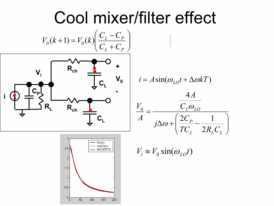
Cool mixer/filter effect∫∫+
+
+
−+
−
+−
=+Tk
TkL
Tk
kTL
LLPL
PL dtCidtCiCRT
CCCCkVkV
)1(
)(
)(
00
21
21
21)()1(
−+∆
=
LLL
P
LOL
CRTCCj
CA
AV
212
40
ω
ω
( ) ∫++≈ dtCiRitVV LchLOi )sin(0 ω
)sin( kTtAi LO ωω ∆+=
+
V0
-
Vi
CL
CL
Rch
RchRL
CPi

Rx Front End• Resistively biased
inverter as LNA.– Av = 2GmLNA /(ωLOCpar)
(20dB)– NF ~9dB
• Passive mixer dissipates little power– Vout: 1-pole LPF at
2FLOCp/CL
– LPF shunts RF signals through switches.
– POBC = -22dBm
Cpar CL
CLRF in
Oscillator+ -
Vlna
+
Vout
-
Vlna: Vout:
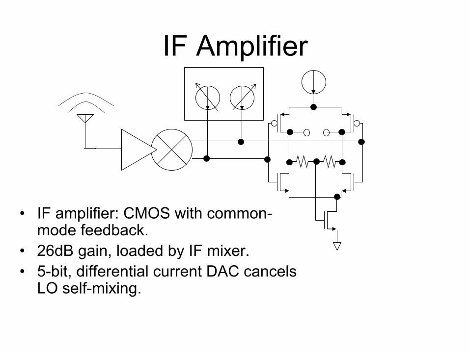
IF Amplifier
• IF amplifier: CMOS with common-mode feedback.
• 26dB gain, loaded by IF mixer.• 5-bit, differential current DAC cancels
LO self-mixing.
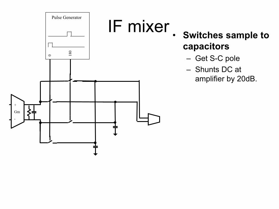
IF mixer• Switches sample to
capacitors – Get S-C pole– Shunts DC at
amplifier by 20dB.
+
Gm
-
0 180
Pulse Generator

+
Gm
-
0 180
Pulse Generator
IF mixer• Switches sample to
capacitors– Get S-C pole– Shunts DC at
amplifier by 20dB.
• IF from divided LO:– I/Q phase split
0 90 180
270
Pulse Generator

+
Gm
-
0 180
Pulse Generator
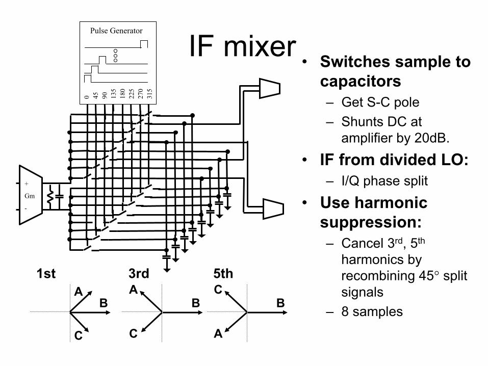
IF mixer• Switches sample to
capacitors – Get S-C pole– Shunts DC at
amplifier by 20dB.
• IF from divided LO:– I/Q phase split
• Use harmonic suppression:– Cancel 3rd, 5th
harmonics by recombining 45° split signals
0 90 180
270
Pulse Generator
C
A
B
5thA
C
B
3rd
B
1stA
C
0 90 180
270
Pulse Generator
+
Gm
-
0 180
Pulse Generator
IF mixer• Switches sample to
capacitors– Get S-C pole– Shunts DC at
amplifier by 20dB.
• IF from divided LO:– I/Q phase split
• Use harmonic suppression:– Cancel 3rd, 5th
harmonics by recombining 45° split signals
– 8 samples
0 45 90 135
180
225
270
315
Pulse Generator
C
A
B
5thA
C
B
3rd
B
1stA
C

0 90 180
270
Pulse Generator
+
Gm
-
0 180
Pulse Generator
IF mixer• Switches sample to
capacitors – Get S-C pole– Shunts DC at
amplifier by 20dB.
• IF from divided LO:– I/Q phase split
• Use harmonic suppression:– Cancel 3rd, 5th
harmonics by recombining 45° split signals
– 8 samples– Weight, sum samples
0 45 90 135
180
225
270
315
Pulse Generator
1
1
1
1.4
1
1.4
C
A
B
5thA
C
B
3rd
B
1stA
C

IF mixer simulations
DC is rejected by 23dB 3rd harmonic mixing is suppressed by 20dB
IF (input) of mixer Baseband (output)

Baseband
• Additional gain and filtering is needed
• Simple Sallen-key filters provide 2 poles.
• Switched-cap amplifiers reject DC, add 12dBgain
• Flip-flop based demodulator clocks in ones/zeros
DQ
+
-D
Q
DQ
DQ
+
-
I
Q
Wanted to demonstrate full bits-to-bits communication, so need an FSK demodulator.

Receiver Results: sensitivity
• NF ~12dB• Sensitivity ~ -93dBm
– From 50Ω+14nH– BER ~10-3, no error
correction• BW = 300kHz• IF = 1.8MHz
Sensitivity vs Power Dissipated
-94
-92
-90
-88
-86
-84
-82
700 800 900 1000 1100 1200 1300 1400
Pin, uW
sens
eitiv
ity, d
Bm
3V
2.75V
2.55V

Receiver Results: Interference
• Wide band 4dB desense: -12dBm• Close-in desense a mix of compression, phase
noise• 3rd, 5th harmonic interference reduced by 40dB.
-100
-80
-60
-40
-20
0
865 875 885 895 905 915 925 935F, MHz
Pint
, dB
m
1st1st
3rd5th
7th 9th15th 17th3rd5th
7th9th15th
17th
signal lvl

Top Level
Inductor Chip

Power summary
tx, nom tx, low rx nom rx lowosc 480 319 336 161Tx 630 464 0 0bias 60 54 90 81divider 90 80 90 80counter 23 23 23 23lna 0 0 378 134IF 0 0 90 52bb 0 0 54 48demod 0 0 75 75total 1283 940 1136 654
Pout 250 100sense, dBm -93 -84
All powers in µW

Link Testing• Two chips communicating through the
air:– 20 kbps– 16 meters through 2 concrete walls– Nominal power
(1.2mW RX, 1.3mW TX)– 100 kbps at shorter range– Battery, antenna, crystal oscillator
inductor, tuning inductor
TX
TX RX

Conclusions
• Ultra-low power, very low cost radios demonstrated:– < 1.3 mW for both Receive and transmit– Only 4 off-chip components needed (< $1)– Purely digital interface.– Showed communication of 20kbps @
16meters indoors.