low power multiplier design using complementary …. kishore kumar et. al. / (ijcse) internationa l...
TRANSCRIPT

A. Kishore Kumar et. al. / (IJCSE) International Journal on Computer Science and Engineering Vol. 02, No. 07, 2010, 2291-2297
Low Power Multiplier Design Using Complementary Pass-Transistor Asynchronous
Adiabatic Logic
A.Kishore Kumar 1 Dr.D.Somasundareswari 2 Dr.V.Duraisamy 3 M.Pradeepkumar 4
1 Lecturer-Department of ECE, 3 Professor & Principal Hindusthan College of Engineering & Technology, Coimbatore, India
2 Professor & Head - Department of ECE, Adithya Institute of Technology, Coimbatore, India 4 Specialist - ECU Development, Robert Bosch, Coimbatore, India
Email: [email protected]
Abstract— In this paper, low power multiplier design using complementary pass-transistor asynchronous adiabatic logic is investigated. Adiabatic circuits are very low power circuits compared with CMOS logic circuits, provided the Power Clock Generators consumes less power and mutilate all low power advantages from the adiabatic logic by consuming large portion of the total power in the clock generation circuitry [1, 2]. Also clock routing is major challenge in the adiabatic, because of routing-delay between the gates. To get out of the problems related to clock generation and synchronous clock routing, a new solution namely asynchronous adiabatic logic [5] is used. Here we have designed, simulated a multiplier with Complementary Pass-Transistor Asynchronous Adiabatic Logic (CPTAAL) which exhibits low power and reliable logical operations comprising the benefit of both asynchronous systems with adiabatic benefits. Compared with the conventional CMOS implementation, this design achieves energy savings from 50% to 74% for clock rates ranging from 100MHz to 300MHz.
Keywords- Low power, Adiabatic, Complementary Pass- transistor Asynchronous Adiabatic
I. INTRODUCTION
Moore’s law describes the requirement of the transistors for VLSI design; it gives the empirical observation that component density and performance of integrated circuits, doubles every year, which was then revised to doubling every two years. With the help of the scaling rules set by Dennard, smart optimization can be achieved by means of timely introduction of new processing techniques in device structures, and materials [9]. To overcome the power and area requirements of the computational complexities, the dimensions of transistors are shrunk into the deep sub-micron region and predominantly handled by process engineering. Driven by tremendous advances in lithography, the 65nm
process technology node featuring approximately 32nm transistors is in vogue right now in high volume production. Moreover the technology migration has become much costly for process the design in terms of its physical design. Developers are forced to bare the tool cost in order to achieve the low power requirements. The transistor cost versus lithographic tool cost is given in the silicon technology future road map, it is noted that transistor cost has decreased seven orders of magnitude whereas tool cost has increased. Thus, the alternate method or migration of process engineering is most invited. The internal capacitance and resistance of transistor structure are shown in Figure 1.
Fig.1. Internal capacitance and resistance of transistor structure
ISSN : 0975-3397 2291

A. Kishore Kumar et. al. / (IJCSE) International Journal on Computer Science and Engineering Vol. 02, No. 07, 2010, 2291-2297
Fig.2. Channel resistance Vs feature size
Fig.3. Channel capacitance Vs feature size
Fig.4. Transistor count Vs Year
Because of the internal, external capacitance and resistance of the semiconductor, external parasitic will be much more influenced while reducing the wafer size. It causes overlapping of both parasitic and channel parameters. It is called parasitic dominance and thus, the industries should look for the alternate material or solution to maintain the internal resistance which decreases with respect to the reduction of wafer size. The channel, parasitic resistance Vs feature size and channel, parasitic capacitance Vs feature size are shown in Figure 2, 3. The Transistor count Vs Year is presented in Figure 4. The physical design is a major challenge in reducing the feature size. But power consumption is a critical issue in the system performance and is listed as one of the main three challenges in International Technology Roadmap for Semiconductor [10].
II. ADIABATIC LOGIC
In recent years, there is a huge demand for low power and low noise digital circuits motivated by VLSI designers to introduce new methods to the design of low power VLSI circuits. There are some classical approaches to reduce the dynamic power such as reducing supply voltage, decreasing physical capacitance and reducing switching activity. These techniques are not fit enough to meet today’s power requirement. However, most research has focused on building adiabatic logic, which is a promising design for low power applications. Adiabatic logic works with the concept of switching activities which reduces the power by giving stored energy back to the supply. Thus, the term adiabatic logic is used in low-power VLSI circuits which implements reversible logic. In this, the main design changes are focused in power clock which plays the vital role in the principle of operation. Each phase of the power clock gives user to achieve the two major design rules for the adiabatic circuit design.
Never turn on a transistor if there is a voltage across it (VDS>0) 1. The inputs must be valid during the
charging/discharging process 2. Make sure every node is reset to the original
stage before performing the next operation.
Never turn off a transistor if there is a current through it (IDS≠ 0) 1. The inputs must be held static throughout the
charging and discharging of capacitances 2. Ensure high resistance results in more energy
consumption
Never pass current through a diode
ISSN : 0975-3397 2292
A. Kishore Kumar et. al. / (IJCSE) International Journal on Computer Science and Engineering Vol. 02, No. 07, 2010, 2291-2297
If these conditions with regard to the inputs, in all the four phases of power clock, recovery phase will restore the energy to the power clock, resulting considerable energy saving. Yet some complexities in adiabatic logic design perpetuate. Two such complexities, for instance are:
Circuit implementation for time-varying power sources needs to be done.
Computational implementation by low overhead circuit structures needs to be followed.
There are two big challenges of energy recovering circuits; first, slowness in terms of today’s standards, second it requires ~50% of more area than conventional CMOS, and simple circuit designs get complicated.
Previously, several adiabatic logic designs such as PAL-2N and 2N-2N2P were proposed and achieved considerable energy savings compared with conventional CMOS design [6]. Also the power clock design will be a major complication to the design, because the whole transistor logic system shares the power clock, then the power clock switching circuit will dissipate the most power in the logic. So we are in need of power reduction techniques by the exploitation of the adiabatic logic. Nowadays multiple phase clocks and clock pipelining are the most followed techniques to reduce power dissipation in the power clocks. In [3], Complementary pass-transistor adiabatic logic circuit is discussed in which, the non adiabatic energy loss of output loads has been completely eliminated by using complementary pass-transistor logic for evaluation phase and transmission gates for energy recovery phase. In [4], adiabatic CPL circuits using two phase power clocks are presented. In [7], energy saving design technique achieved by latched pass-transistor with adiabatic logic is presented. Many research efforts in the adiabatic logic have been introduced to reduce the power dissipation of VLSI circuits [1-8]. In [11], a low power multiplier using 4-2 compressor based on adiabatic CPL circuit is described. In this paper we have investigated a low power multiplier design, using complementary pass-transistor asynchronous adiabatic logic.
III. ASYNCHRONOUS ADIABATIC LOGIC
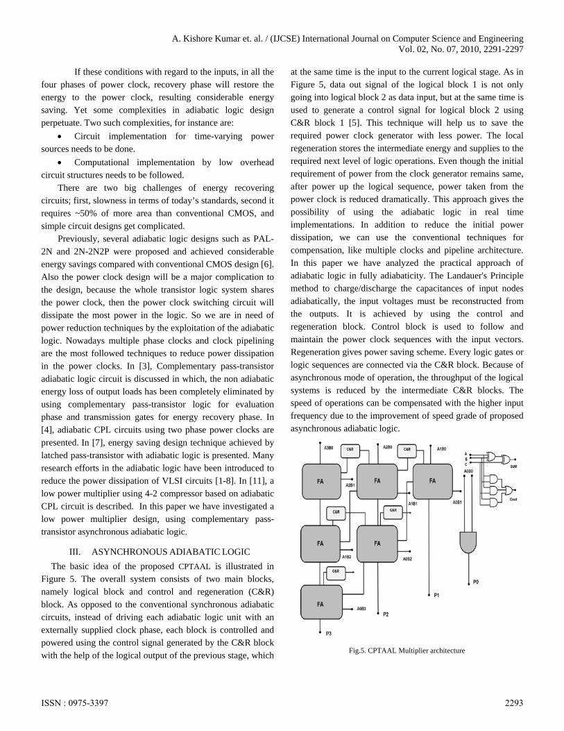
The basic idea of the proposed CPTAAL is illustrated in Figure 5. The overall system consists of two main blocks, namely logical block and control and regeneration (C&R) block. As opposed to the conventional synchronous adiabatic circuits, instead of driving each adiabatic logic unit with an externally supplied clock phase, each block is controlled and powered using the control signal generated by the C&R block with the help of the logical output of the previous stage, which
at the same time is the input to the current logical stage. As in Figure 5, data out signal of the logical block 1 is not only going into logical block 2 as data input, but at the same time is used to generate a control signal for logical block 2 using C&R block 1 [5]. This technique will help us to save the required power clock generator with less power. The local regeneration stores the intermediate energy and supplies to the required next level of logic operations. Even though the initial requirement of power from the clock generator remains same, after power up the logical sequence, power taken from the power clock is reduced dramatically. This approach gives the possibility of using the adiabatic logic in real time implementations. In addition to reduce the initial power dissipation, we can use the conventional techniques for compensation, like multiple clocks and pipeline architecture. In this paper we have analyzed the practical approach of adiabatic logic in fully adiabaticity. The Landauer's Principle method to charge/discharge the capacitances of input nodes adiabatically, the input voltages must be reconstructed from the outputs. It is achieved by using the control and regeneration block. Control block is used to follow and maintain the power clock sequences with the input vectors. Regeneration gives power saving scheme. Every logic gates or logic sequences are connected via the C&R block. Because of asynchronous mode of operation, the throughput of the logical systems is reduced by the intermediate C&R blocks. The speed of operations can be compensated with the higher input frequency due to the improvement of speed grade of proposed asynchronous adiabatic logic.
Fig.5. CPTAAL Multiplier architecture
ISSN : 0975-3397 2293

A. Kishore Kumar et. al. / (IJCSE) International Journal on Computer Science and Engineering Vol. 02, No. 07, 2010, 2291-2297
A. Control & Regeneration (C&R) Block
The C&R block is given in Figure 6. In the proposed multiplier circuit, Asynchronous operation has been achieved by the control and regeneration part, which controls and regenerate the energy, required for the next operation to the next logical block. The energy of the system will be circulating among the logical circuits and the minimum power is required from the power clock generator for the operation. In general the regenerated signal is stored and circulated between the C&R and logical part; thus, there won’t be much power reverse to the power clock system. It helps to reduce the power clock system switching losses. CPTAAL gates are used, to design logical blocks and the pass-transistor logic implementation, has been found the best solution for the design of C&R block in terms of power efficiency and functionality. The NOR portion of the OR gate is acting as the control part where as the NOT portion is not only making the desired logical inversion, but at the same time, is performing the regeneration of the signal. The regenerated signal energy will be used in the next logic circuit for the sequential operation. The NOT portion will again regenerate the signal where as the operation gets completed.
Fig.6. C & R block
The construction of the C&R promotes the local storage of the energy and switching circuit for the recovery. The power reduction is not achieved in C&R block due to the usage of conventional CMOS OR logic rather than the adiabatic logic. However 60% to 70% of power saving and 1/3 of the speed improvement is achieved compared to the adiabatic combined with the power clock generator.
B. Asynchronous Adiabatic Multiplier
Asynchronous adiabatic multiplier logic uses Complementary pass-transistor logical block with C&R structures. It has been designed and tested to get the best power efficiency out of the CPTAAL system. A simple implementation of the CPTAAL is depicted. It is a full adder, with the logical part designed using CPTAAL, and whereas the control part of the C&R block and regeneration part is made of pass-transistor logic. The full adder logic diagram is presented in the Figure 7. Asynchronous adiabatic 8 bit multiplier is presented in Figure 8.
Fig.7. Full Adder Logic Diagram
Fig.8. Asynchronous adiabatic 8 bit multiplier
ISSN : 0975-3397 2294
A. Kishore Kumar et. al. / (IJCSE) International Journal on Computer Science and Engineering Vol. 02, No. 07, 2010, 2291-2297
C. Low Power Clocking System
Figure 9, 10 shows the operational benefits of Synchronous clock system Vs Asynchronous clock system. The synchronous system uses the clock source globally, i.e. single clock is shared and restored by the large number of logical gates in parallel, and here switching loss of the power clock generator is more as in the CMOS circuit operation. The simple structure of the pass-transistor logic makes it easy to tweak the sizing of transistors to get the desired charging and discharging time and hence the slope of the output control signal minimizes the power. In asynchronous clock system, the clock energy is locally stored in the C&R block and it has been used for subsequent gates, the loss of energy of each operation will be taken from its clock source.
Fig.9. Synchronous supply Clock
Fig.10. Asynchronous supply Clock
IV. SIMULATION RESULTS AND PERFORMANCE
ANALYSIS
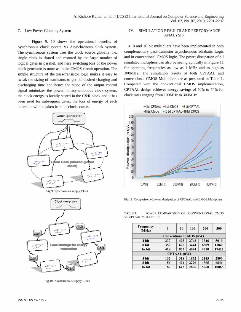
4, 8 and 16 bit multipliers have been implemented in both complementary pass-transistor asynchronous adiabatic Logic and in conventional CMOS logic. The power dissipation of all simulated multipliers can also be seen graphically in Figure 11 for operating frequencies as low as 1 MHz and as high as 300MHz. The simulation results of both CPTAAL and conventional CMOS Multipliers are as presented in Table 1. Compared with the conventional CMOS implementation, CPTAAL design achieves energy savings of 50% to 74% for clock rates ranging from 100MHz to 300MHz.
Fig.11. Comparison of power dissipation of CPTAAL and CMOS Multipliers
TABLE I. POWER COMPARISION OF CONVENTIONAL CMOS
VS CPTAAL MULTIPLIER
Frequency (MHz)
1 10 100 200 300
Conventional CMOS (nW) 4 bit 237 493 2748 3346 5010 8 bit 359 676 3444 6809 11843 16 bit 418 837 4044 9310 17412
CPTAAL (nW) 4 bit 132 318 1832 2145 2896 8 bit 156 494 2296 4365 6846 16 bit 187 643 2696 5968 10065
ISSN : 0975-3397 2295

A. Kishore Kumar et. al. / (IJCSE) International Journal on Computer Science and Engineering Vol. 02, No. 07, 2010, 2291-2297
TABLE II. COMPARISION OF TRANSISTOR COUNT
No. Of
Bits
No. Of Transistors
CMOS CPTAAL % increase
4 bit 560 632 12.9 8 bit 1176 1392 18.4
16 bit 2464 3118 26.5 The transistor count of 4, 8 and 16 bit multipliers is compared with conventional CMOS design and CPTAAL design and is tabulated in Table 2.
Fig.12. Asynchronous adiabatic Multiplier simulation results
The simulation results of asynchronous adiabatic multiplier are shown in Figure 12.Tanner EDA tool with SPICE support is used for simulation.
V. CONCLUSION
In this paper we have presented a novel methodology for designing low power multipliers by Complementary Pass-transistor Asynchronous Adiabatic Logic (CPTAAL). The performance of this design is analyzed with 4 bit, 8 bit, and 16 bit multipliers and compared with the Conventional CMOS Logic Design. It was determined that for frequencies between 100MHz to 300MHz, asynchronous adiabatic multiplier circuits consumes much less energy than the Conventional CMOS Design. This approach confirms the feasibility of asynchronous adiabatic multiplier circuits in low power applications
REFERENCES
[1] Alex G. Dickinson and John S. Denker, “Adiabatic Dynamic Logic”, IEEE Journal of solid-state circuits, vol. 30, no. 3, march 1995.
[2] Arsalan, M. Shams, M., “Charge-recovery power clock generators for adiabatic logic circuits”, VLSI Design, 2005. 18th International Conference on, vol., no.pp. 171- 174, 3-7 Jan. 2005.
[3] Jianping Hu, Tiefeng Xu and Hong Li, “A lower power register file based on complementary pass-transistor adiabatic logic”, IEICE Trans on Inf. & Sys.vol.E88-D(7),pp 1479-1485, 2005.
[4] Dai Jing. Hu Jianping, Zhang Weiqiang, Wang Ling, “Adiabatic CPL circuits for sequential logic systems”, IEEE MWSCAS’06, pp713-717, Aug 2006.
[5] Muhammad Arsalan and Maitham Shams, “Asynchronous Adiabatic Logic”, vol., no.pp. 3720- 3723, IEEE 2007.
[6] Jian Ping Hu; Weijang Zhang; Yinshui Xia;“Complementary pass-transistor adiabatic logic and sequential circuits using three-phase power supply” ,Circuits and Systems, 2004. MWSCAS '04. The 2004 47th Midwest Symposium on Volume 2, 25-28 July 2004 Page(s):II-201 - II-204 vol.2.
[7] Junyoung Park; Sung Je Hong; Jong Kim. “Energy saving design technique achieved by latched pass-transistor adiabatic logic” Circuits and Systems, 2005. ISCAS 2005. IEEE International Symposium on 23-26 May 2005 Page(s):4693 - 4696 Vol. 5.
[8] Jianping Hu; Weiqiang Zhang; Xien Ye; Yinshui Xia; “Low power adiabatic logic circuits with feedback structure using three-phase power supply” Communications, Circuits and Systems, 2005. Proceedings. 2005 International Conference on Volume 2, 27-30 May 2005.
[9] Dennard, R.H., et al., IEEE Journal on Solid State Circuits, 9,256, 1974.
[10] Scott.E.Thompson, Srivatsan Partha Sarathy,”Moore’s law: The future of Si Microelectronics” Materials Today, Volume 9, Number 6. June 2006.
[11] Ling Wang, Jianping Hu, and Jing Dai, “ A Low power Multiplier Using Adiabatic CPL Circuits”, IEEE International Symposium on Integrated Circuits, vol., no.pp. 21-24, 2007.
ISSN : 0975-3397 2296

A. Kishore Kumar et. al. / (IJCSE) International Journal on Computer Science and Engineering Vol. 02, No. 07, 2010, 2291-2297
AUTHORS PROFILE
A.Kishore Kumar received his B.E. Degree in Electronics & Instrumentation Engineering (2002) and M.E., Degree in Communication Systems (2008), currently doing Ph.D. in Anna University of Technology, Coimbatore. He has 5 years of teaching experience and 2 years of industry (R&D) experience, currently working as Lecturer in the Department of Electronics and Communication Engineering at Hindusthan College of Engineering & Technology, Coimbatore. He is a life member of ISTE and associate member of IETE. He has published more than 15 research papers in Conferences. His research interest includes Low power VLSI design, Analog VLSI Design and Instrumentation systems. Dr.D.Somasundareswari received her B.E. Degree in Electrical & Electronics Engineering (1994) and M.E., Degree in Electrical Machines (2001) and Ph.D. Degree (2008) from Anna University, Chennai. She has 17 years of teaching experience and currently working as Professor and Head, Department of Electronics and Communication Engineering at Adithya Institute of Technology, Coimbatore. She is a life member of ISTE, SSI and member of IE. She has published more than 30 research papers in the Journals and Conferences. Her research interest includes Soft computing, Electrical machines and VLSI Design. Dr.V.Duraisamy received his B.E. Degree in Electrical & Electronics Engineering (1991) and M.E., Degree in Electrical Machines (1997) and Ph.D. Degree (2006) from Anna University, Chennai. He has 21 years of teaching experience and currently working as Professor and Principal at Hindusthan College of Engineering and Technology, Coimbatore. He is a life member of ISTE, SSI and member of IE. He has published more than 40 research papers in the Journals and Conferences. His research interest includes Soft computing, Electrical machines. M.Pradeepkumar received his B.E. Degree in Electronics & Communication Engineering (2003) and M.E., Degree in VLSI Design (2009). He has 7 years of industry (R&D) experience, currently he is working in Robert Bosch India as specialist – ECU Development. He has published more than 15 research papers in the Conferences. His research interest includes Low power VLSI design, Analog VLSI Design and Automotive electronics.
ISSN : 0975-3397 2297