low power electronics - pds: small bodies node home
TRANSCRIPT
Low Power Electronics
DS1 Technology Validation Report Flight Qualifying Sub-0.25-µm
Fully Depleted SOI CMOS Technology
Richard P. D’Onofrio — [email protected] Dr. Craig L. Keast — [email protected] Antonio M Soares — [email protected] Dr. Peter W. Wyatt — [email protected] MIT Lincoln Laboratory 244 Wood Street Lexington, MA 02420-9108 Phone: (781) 981-7880 FAX: (781) 981-7889

Deep Space 1 Technology Validation Report—Low Power Electronics
iii
Table of Contents Section Page Extended Abstract .......................................................................................................................................iv Fact Sheet.....................................................................................................................................................v 1.0 Introduction............................................................................................................................................1 2.0 Technology Description .........................................................................................................................1
2.1 What Is It?...............................................................................................................................................................................................1 2.2 Key Validation Objectives ...................................................................................................................................................................3 2.3 Expected Performance Envelope ........................................................................................................................................................3 2.4 Detailed Test Description.....................................................................................................................................................................3 2.5 Technology Interdependencies............................................................................................................................................................4 2.6 Testing .....................................................................................................................................................................................................4 2.7 Test Result Comparison........................................................................................................................................................................6
3.0 Technology Validation Summary ..........................................................................................................16 4.0 Technology Application for Future Missions .......................................................................................16 5.0 Acknowledgments.................................................................................................................................16 6.0 List of References.................................................................................................................................17
Figures Figure Page Figure 1. Schematic Cross Section of <0.25-µm FDSOI n-channel and p-channel Transistors........................................................ 1 Figure 2. Ring-oscillator Stage Delay vs. Voltage with Fanout = 1 for the 0.25-µm FDSOI Technology...................................... 2 Figure 3. Total-Dose Test Results for an 8.0-µm/ 0.25-µm n-Channel Device.................................................................................... 2 Figure 4. Photograph of the Low-power Experiment 6u VME–style Test Board ................................................................................ 3 Figure 5. Transistor Test Schematic ............................................................................................................................................................. 3 Figure 6. Transistor/Ring Oscillator Test Overview.................................................................................................................................. 4 Figure 7. LPE Board Overview..................................................................................................................................................................... 5 Figure 8. N-Channel Transistor (Vth); ~2-mV A/D Converter Resolution (left-hand Y-axis).......................................................... 7 Figure 9. N-channel Transistor (Leakage1) ................................................................................................................................................ 7 Figure 10. N-channel Transistor (Leakage2) .............................................................................................................................................. 8 Figure 11. N-channel Transistor (Leakage3) .............................................................................................................................................. 8 Figure 12. N-channel Transistor (Drive Current1)..................................................................................................................................... 9 Figure 13. N-channel Transistor (Drive Current2)..................................................................................................................................... 9 Figure 14. N-channel Transistor (gmSat) .................................................................................................................................................. 10 Figure 15. N-channel Transistor (Gds) ...................................................................................................................................................... 10 Figure 16. P-channel Transistor (Vth); ~2-mV A/D Converter Resolution (left-hand Y-axis) ....................................................... 11 Figure 17. P-channel Transistor (Leakage1) ............................................................................................................................................. 11 Figure 18. P-channel Transistor (Leakage2) ............................................................................................................................................. 12 Figure 19. P-channel Transistor (Leakage3) ............................................................................................................................................. 12 Figure 20. P-channel Transistor (Drive Current1) ................................................................................................................................... 13 Figure 21. P-channel Transistor (Drive Current2) ................................................................................................................................... 13 Figure 22. P-channel Transistor (gmSat) ................................................................................................................................................... 14 Figure 23. P-channel Transistor (Gds)....................................................................................................................................................... 14 Figure 24. L = 0.25-µm 97-Stage Ring Oscillator 1 ................................................................................................................................ 14 Figure 25. L = 0.25-µm 97-Stage Ring Oscillator 2 ................................................................................................................................ 15 Figure 26. L = 0.25-µm 97-Stage Ring Oscillator 3 ................................................................................................................................ 15 Figure 27. L = 0.25-µm 97-Stage Ring Oscillator 4 ................................................................................................................................ 16

Deep Space 1 Technology Validation Report—Low Power Electronics
iv
Appendices Appendix Page Appendix A: Telemetry Channels ...............................................................................................................18 Appendix B: Date of Turn-on/Frequency of Data Capture ...........................................................................19

Deep Space 1 Technology Validation Report—Low Power Electronics
v
EXTENDED ABSTRACT The future of deep-space exploration is dependent on the research and development of new technologies that will allow designers to build low-power, lightweight space systems and peripherals. The focus of this technology validation experiment is to characterize the effects of the space environment on a DARPA-sponsored, sub-0.25-µm, fully depleted silicon-on-insulator (FDSOI) complementary metal-oxide semiconductor (CMOS) technology developed at MIT Lincoln Laboratory. FDSOI technology offers the advantage of providing high performance (>1 GHz operation) from a sub-2.0-V power supply. The resulting reduction in power consumption (~5 times less power than the corresponding 0.25-µm bulk CMOS technology), coupled with the SOI technology’s inherent resistance to latchup, make this an attractive choice for the design of integrated circuits used in hardware systems for deep-space exploration. In addition, the increased transistor-packing densities realized with SOI technology allow for the fabrication of smaller, lighter, higher-performance devices. A first step towards validating the sub-0.25-µm FDSOI process as a key technology for deep-space application lies in the examination and analysis of FDSOI behavior at the transistor level. The collection of key parametric data from the measurement of 8.0-µm/0.25-µm n-channel and p-channel transistors will serve as a sound predictor for how well circuits developed with this technology will perform in space.
One of the major risks associated with electronic technologies in the space environment is operational failure due to total dose radiation. Our approach with the Low Power Flight Experiment (LPE) is to observe the properties of test devices where no attempt has been made in either processing or packaging to optimize performance for the radiation environment. We are instead interested in characterizing the sub-0.25-µm FDSOI baseline process developed at MIT Lincoln Laboratory and verifying that the inherent radiation-hardened qualities of the technology that have been examined through ground testing hold true in the space environment. FDSOI parametric testing on Deep Space 1 (DS1) is performed by a board designed to emulate the tasks of a semiconductor parameter analyzer. The sub-0.25-µm FDSOI test chip is mounted on this board. All board components, with the exception of the test chip, are radiation-hardened so that all changes in behavior can be isolated to the test chip. After nearly one year in space, the technology continues to function, yielding parametric data that is very similar to data taken before the launch. The total ionizing dose (TID) exposure of the test chip has had very little effect on function and performance. The results of the LPE have shown that transistor characteristics and performance are minimally affected by the space environment. This insight into the fundamental building blocks of circuit design will prove to be invaluable when creating more complex SOI test circuits for further space qualification.
Deep Space 1 Technology Validation Report—Low Power Electronics
vi
Low Power Flight Experiment
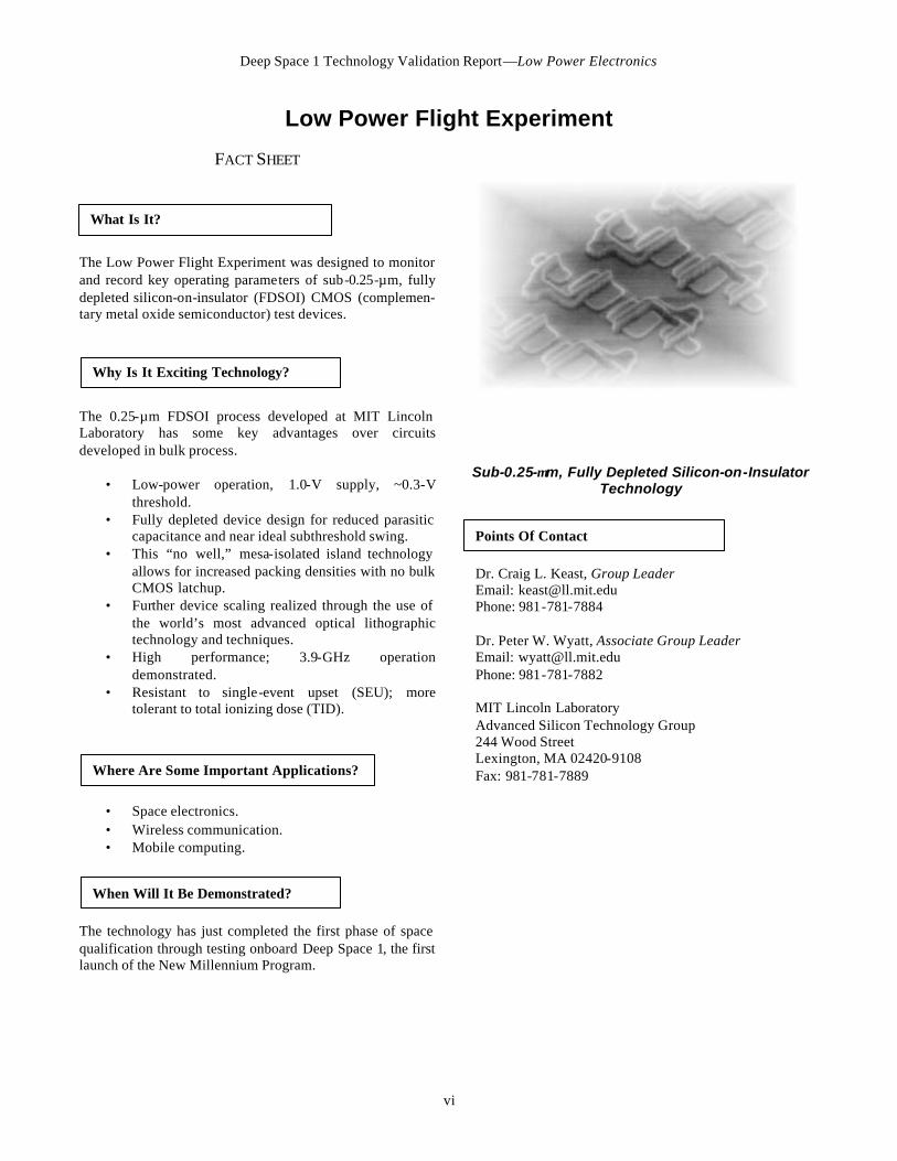
FACT SHEET The Low Power Flight Experiment was designed to monitor and record key operating parameters of sub-0.25-µm, fully depleted silicon-on-insulator (FDSOI) CMOS (complemen-tary metal oxide semiconductor) test devices. The 0.25-µm FDSOI process developed at MIT Lincoln Laboratory has some key advantages over circuits developed in bulk process.
• Low-power operation, 1.0-V supply, ~0.3-V threshold.
• Fully depleted device design for reduced parasitic capacitance and near ideal subthreshold swing.
• This “no well,” mesa-isolated island technology allows for increased packing densities with no bulk CMOS latchup.
• Further device scaling realized through the use of the world’s most advanced optical lithographic technology and techniques.
• High performance; 3.9-GHz operation demonstrated.
• Resistant to single-event upset (SEU); more tolerant to total ionizing dose (TID).
• Space electronics. • Wireless communication. • Mobile computing.
The technology has just completed the first phase of space qualification through testing onboard Deep Space 1, the first launch of the New Millennium Program.
Sub-0.25-µm, Fully Depleted Silicon-on-Insulator Technology
Dr. Craig L. Keast, Group Leader Email: [email protected] Phone: 981-781-7884 Dr. Peter W. Wyatt, Associate Group Leader Email: [email protected] Phone: 981-781-7882 MIT Lincoln Laboratory Advanced Silicon Technology Group 244 Wood Street Lexington, MA 02420-9108 Fax: 981-781-7889
What Is It?
Why Is It Exciting Technology?
Where Are Some Important Applications?
When Will It Be Demonstrated?
Points Of Contact

Deep Space 1 Technology Validation Report—Low Power Electronics
1
Low Power Electronics DS1 Technology Validation Report Flight Qualifying Sub-0.25-µm, Fully Depleted SOI CMOS Technology
Richard P. D’Onofrio, Craig L. Keast, Antonio M. Soares, Peter W. Wyatt
Lincoln Laboratory, Massachusetts Institute of Technology 244 Wood Street, Lexington, MA 02173-9108
(781) 981-2573
1.0 INTRODUCTION The new millennium brings with it exciting technical challenges in the area of circuit design. Deep-space travel, wireless communication, and mobile computing are just a few examples of important applications that demand a core of low-power, high-performance electronic components. The design rule constraints of bulk complementary metal-oxide semiconductor (CMOS) technology have limited just how far researchers can go in reducing power consumption while maintaining and improving performance. Fully depleted silicon-on-insulator (FDSOI) technology promises to be an important area of research for the continued advance of low-power, high-performance electronics. The combination of transistor mesa-island isolation along with the feature-size scaling available through advances in lithographic equipment and techniques, allow for the design of smaller, faster, lower-power circuits. In addition, the technology's inherent resistance to latchup makes it particularly attractive for space application. The New Millennium Program has provided the opportunity to begin the process of flight-qualifying this technology for deep-space application.
2.0 TECHNOLOGY DESCRIPTION 2.1 What Is It? 2.1.1 Fully Depleted 0.25-µm SOI Technology—Figure 1 shows a schematic cross section of an n-channel and p-channel transistor fabricated in the 0.25-µm FDSOI CMOS technology. The starting silicon active layer thickness is thinned to 61 nm by thermal oxidation. After processing, the final active-area thickness is approximately 50 nm. Device isolation is by mesa-etching followed by sidewall-oxidation. The 10 nm of SiO2 topped by 100 nm of Si3N4 are patterned and plasma-etched along with the silicon layer. A 45° sidewall “channel stop” implant is followed by a 40-nm sidewall oxidation. After island doping by implantation through a 7-nm sacrificial oxide, a 7-nm gate oxide is grown at 850° C followed by a 225-nm undoped amorphous Si gate deposition. The gate electrode is then patterned, plasma etched and reoxidized at 800° C. A medium-doped drain implant is followed by a 120-nm spacer oxide deposition and etch followed by a source/drain implant. The source/drain implant, which also dopes the polysilicon gate electrodes, is activated with a 950° C, 30-s annealing.
50 nm Si 7 nm Gate Oxide
170 nm Buried Oxide
Silicon Handle Wafer
n-Channel p-Channel
n+ n+ p n + poly
p+ p+ n p + poly
Figure 1. Schematic Cross Section of <0.25-µm FDSOI n-Channel and p-Channel Transistors
A titanium-capped cobalt salicide process contacts the 50-n m-thick silicon regions and straps the p+, n+, and undoped polysilicon gates [1]. The back end consists of a fully planar, three-level, metal interconnect process that incorporates damascene hot aluminum plugs at contacts, via 1 and via 2, and chemical mechanical polished (CMP) plasma-enhanced chemical vapor deposition (PECVD) tetraethylorthosilicate (TEOS) oxide intermetal dielectric. Figure 2 shows the inverter stage delay vs. power supply voltage for a 97-stage ring oscillator fabricated in the FDSOI technology. This process results in a 25-ps stage delay at 2 V, and when clocked at the same level of performance as a 2.5-V, 0.25-µm bulk CMOS technology, the FDSOI CMOS offers a five-times-less reduction in power. To date 85 different digital, analog, and mixed-mode circuits have been fabricated in this technology as part of the DARPA-funded low-power, high-performance multiproject-run research fabrication service at MIT Lincoln Laboratory. Typical digital operation is from 600 mV to 2 V for this 400-mV threshold technology, with clock speeds generally over 100 MHz at 1.0 V and in excess of 1 GHz with a 2-V power supply [2]. The 0.25-µm FDSOI CMOS technology has been used to fabricate a data generation/ acquisition process-benchmarking test circuit. The 0.25-µm FDSOI technology had similar performance to the Vitesse

Deep Space 1 Technology Validation Report—Low Power Electronics
2
H-GaAs-3 process technology (950 MHz vs. 1 GHz operation). However, the FDSOI circuit consumed 45 times less power than the GaAs circuit (43 mW vs. 2 W).
3.5 3.0 2.5 2.0 1.5 1.0 0.5 0.0 0
25
50
75
100
125
150
Power Supply (V)
Sta
ge
Del
ay (
ps)
FDSOI Power ~20x Lower
LL 0.25 µm FD-SOI
0.35 µm Bulk CMOS
Figure 2. Ring-oscillator Stage Delay vs. Voltage
with Fanout = 1 for the 0.25-µm FDSOI Technology. Also shown is the data point for a commercially available 0.25-µm, 2.5-V bulk CMOS technology.
2.1.2 Preliminary Radiation Performance—The 0.25-µm FDSOI CMOS process was designed for low-power, high-performance operation. Radiation characteristics of the process were not critical design parameters during the process development cycle; i.e., nothing was done to optimize radiation performance. However, given that the process uses thin gate oxides (7 nm), has fully oxide-isolated transistors, and is not susceptible to parasitic bipolar latch-up (no wells), there is the potential for good total dose radiation resistance. In order to get a baseline on the total-dose-radiation performance, testing was performed on an ARACOR Model 4100 Semiconductor Irradiation System with an 10-keV X-ray source. The dose rate was 10 krad (Si) per minute for 0 to 200 krad and 130 krad (Si) per minute for 200 to 1000 krad. The devices were measured immediately after irradiation. Figure 3a shows the Id vs. Vgs curves for an 8-µm/0.25-µm n-channel device biased with 1.0 V on the gate and 0.0 V on the source, drain, and substrate. The threshold shift was ~130 mV after 1 Mrad (Si). Figure 3b shows the same device; however, in these curves the channel of the transistor from the radiation-induced measurement was performed with the addition of a –30-V substrate-wafer bias. This –30-V wafer bias accumulates the back channel
2.0 1.5 1.0 0.5 0.0 -0 . 5-1 . 01 0 -14
1 0 -13
1 0 -12
1 0 -11
1 0 -10
1 0 -9 1 0 -8 1 0 -7 1 0 -6 1 0 -5 1 0 -4 1 0 -3
Initial 5 krad(Si) 10 krad(Si) 20 krad(Si) 50 krad(Si) 100 krad(Si ) 200 krad(Si ) 1000 krad(Si) 500 krad(Si )
rksoi- 1, w3, die 4,3
(a)
2.0 1 . 5 1 . 0 0.5 0.0 -0.5 -1 . 0
10 -14
10 -13
10 -12
10 -11
10 -10
10 -9 10 -8 10 -7 10 -6 10 -5 10 -4 10 -3
In i t ia l 5 krad(Si) 10 krad(Si) 20 krad(Si) 50 krad(Si) 200 krad(Si) 500 krad(Si) 1000 krad(Si )
100 krad(Si)
rkso i-1 , w3, d ie
(b)
2.0 1.5 1.0 0.5 0.0 -0.5 -1.0 10 -14 10 -13 10 -12 10 -11 10 -10 10 -9 10
-8 10 -7 10 -6 10 -5 10 -4 10 -3
Initial 5 krad(Si) 10 krad(Si) 20 krad(Si) 50 krad(Si) 100 krad(Si) 200 krad(Si) 500 krad(Si) 1000 krad(Si)
rksoi-1, w3, die 3,3
Gate Voltage (volts)
Dra
in C
urre
nt (
amps
)
(c) Figure 3. Total -Dose Test Results for an 8.0-µm/
0.25-µm n-Channel Device: (a) biased in the “on” state during irradiation, (b) “on” state
bias measured with –30 V on the substrate (c) “pass-gate” bias
Gate Voltage (volts)
Gate Voltage (volts)
Dra
in C
urr
ent (
amp
s)
Dra
in C
urr
ent (
amp
s)
FDSOI Power ~5x Lower
LL 0.25µm FDSOI
0.25µm Bulk CMOS

Deep Space 1 Technology Validation Report—Low Power Electronics
3
of the transistor, effectively shielding the front charging effects of the buried oxide. Under these bias conditions the IV curves do not shift after radiation treatment, indicating that the radiation-induced shift in Figure 3a is the result of buried oxide charge. Figure 3c shows a “pass gate-biased” device with 1.0 V on the drain, 0.0 V on the source, gate, and substrate-measured with 0 V on the substrate. For this bias condition the threshold shift is ~500 mV at 1 Mrad (Si). 2.2 Key Validation Objectives The key objective of the Low Power Flight Experiment (LPE) is to monitor changes in FDSOI device characteristics over the course of the Deep Space 1 (DS1) mission, and to correlate those changes with total-dose-radiation measurements sampled at the time the experiments were performed. 2.2.1 N-channel Transistor Characteristic Measurements— 1. Threshold Voltage 2. Drain-Source Leakage (Vds = 1.0 V, Vgs = 0.0 V) 3. Drain-Source Leakage (Vds = 2.0 V, Vgs = 0.0 V) 4. Drain-Source Leakage (Vds = 2.0 V, Vgs = –0.5 V) 5. Drive Current (Vds = 1.0 V, Vgs = 1.0 V) 6. Drive Current (Vds = 2.0 V, Vgs = 2.0 V) 7. Saturation Transconductance 8. Drain-Source Output Conductance. 2.2.2 P-channel Transistor Characteristic Measurements— 1. Threshold Voltage 2. Drain-Source Leakage (Vds = –1.0 V, Vgs = 0.0 V) 3. Drain-Source Leakage (Vds = –2.0 V, Vgs = 0.0 V) 4. Drain-Source Leakage (Vds = –2.0 V, Vgs = 0.5 V) 5. Drive Current (Vds = –1.0 V, Vgs = –1.0 V) 6. Drive Current (Vds = –2.0 V, Vgs = –2.0 V) 7. Saturation Transconductance 8. Drain-Source Output Conductance. 2.2.3 Performance—In addition to monitoring key transistor properties, the LPE also addresses the issue of performance monitoring. By sampling the output frequency of four 97-stage ring oscillators, we can evaluate how stage delay is affected by the space environment. 2.3 Expected Performance Envelope It is expected that the sub-0.25-µm FDSOI transistor properties, as well as ring-oscillator performance, will be minimally affected by exposure to the total dose radiation seen by the spacecraft. 2.4 Detailed Test Description 2.4.1 Overview—In order to begin the process of space qualification, MIT Lincoln Laboratory fabricated a test integrated circuit consisting of n-channel and p-channel transistors as well as a group of 97-stage ring oscillators.
This low-power test chip was integrated into a test system that was designed to periodically monitor and record any changes in the basic characteristics of the transistors as well as evaluating changes in switching speed by sampling ring oscillator output frequencies as they are exposed to the space environment. The output of dosimeter and temperature-sensing circuits are sampled and recorded at each step of the test sequence to correlate the effects of thermal variation and total dose radiation. The test system is fabricated on a 6u VME–style board using radiation-hardened components (Figure 4). The board is a category 3 experiment attached to a non-essential bus of the DS1 via a dual-redundant 1553B interface, with a Boeing SMARTIO integrated circuit being used as the protocol controller.
Figure 4. Photograph of the Low-power Experiment 6u VME–style Test Board
2.4.2 Device Testing—A series of MOS transistor measurements are made through the independent control of the gate, drain, and source nodes of each transistor, with connectivity achieved through a low noise, low leakage, programmable switching matrix (Figure 5). Programmable
Figure 5. Transistor Test Schematic
Boeing SMARTIO
FDSOI Test Chip

Deep Space 1 Technology Validation Report—Low Power Electronics
4
voltage and current sources supply the “transistor under test” with appropriate bias conditions for the measurement being performed. Transistor characteristics such as threshold, conductance, and leakage are sampled and processed by an A/D converter. The SMARTIO ASIC is equipped with frequency-to-digital conversion capability, providing an accurate means of sampling ring oscillator output frequency. (See Figure 6 and Figure 7). The spacecraft begins an LPE test by configuring the SMARTIO ports and sending a “begin” instruction. At this point, experiment control is transferred to the LPE onboard sequencer that cycles through the test instructions stored in ROM. The instructions for any given test set up the appropriate switch and voltage/current configurations. Results from all experiments are stored in onboard memory along with dosimeter and temperature information, where they are then transferred to the spacecraft’s solid-state recorder for transmission down to Earth. 2.5 Technology Interdependencies The LPE is “piggybacked” with the power activation and switching module (PASM), to which the LPE supplies power. In addition, the LPE’s Boeing SMARTIO protocol
controller provides the communication conduit between the PASM and the spacecraft. 2.6 Testing The LPE monitors the following eight key transistor parameters that will provide insight into the health of the devices. 1. Threshold Voltage—Transistor “turn-on” voltage
defined as Vgs @ Ids = W/L ∗ 0.1 µA. 2. Drain-Source Leakage1—Transistor subthreshold
leakage with 0.0 V applied to gate, 1.0 V (– polarity for p-channel devices) applied to drain, source grounded.
3. Drain-Source Leakage2—Transistor subthreshold leakage with 0.0 V applied to gate, 2.0 V (– polarity for p-channel devices) applied to drain, source grounded.
4. Drain-Source Leakage3—Transistor drain diode leakage with –0.5 V (+ polarity for p-channel devices) applied to gate, 2.0 V (– polarity for p-channel devices) applied to drain, source grounded.
5. Drive Current1—Transistor current drive capability with 1.0 V (– polarity for p-channel devices) applied to gate, 1.0 V (– polarity for p-channel devices) applied to drain, source grounded.
Figure 6. Transistor/Ring Oscillator Test Overview
ANALOGMUX
SMARTIO FDCPORT
SMARTIO ADDRESSCONTROL
ANALOGMUX
DAC1
DAC2
A/D12
TO ON-BOARDMEMORY
8
8
500 OHMS
5K OHMS
50K OHMS
500K OHMS
5M OHMS
MULTIPLIER POWER
LPE Test Chip

Deep Space 1 Technology Validation Report—Low Power Electronics
5
1553 BUS (Spacecraft Communication)
1553XCVR
1553XCVR
SMART I/OASIC
FPGA
P0
P1P2P3
MEMORY
PROM
6U VME BOARD
RAD MON
TEMP
SWITCHING MATRIX &INTERFACE I/O
40MHz
Figure 7. LPE Board Overview
6. Drive Current2—Transistor current drive capability
with 2.0 V (– polarity for p-channel devices) applied to gate, 2.0 V (– polarity for p-channel devices) applied to drain, source grounded.
7. Saturation Transconductance—The effect of gate voltage on output current in the saturation region at Vds = Vgs = 2.0 V (– polarity for p-channel devices).
8. Drain-Source Output Conductance—Transistor channel conductance in saturation at Vds = Vgs = 2.0 V (– polarity for p-channel devices).
The LPE also monitors the output frequency of four 97-stage ring oscillators at a 2.0-V power supply. Frequency-to-digital conversion is performed by the Boeing SMARTIO integrated circuit 2.6.1 Ground Testing—The results of 8.0-µm/0.25-µm n-channel transistor ground measurements are as follows: 1. (Vth) Threshold Voltage = 220 mV 2. (Lkg1) Drain-Source Leakage (Vds = 1.0 V,
Vgs = 0.0 V) = 415 nA 3. (Lkg2) Drain-Source Leakage (Vds = 2.0 V,
Vgs = 0.0 V) = 7.1 µA
4. (Lkg3) Drain-Source Leakage (Vds = 2.0 V, Vgs = –0.5 V) = 13.4 nA
5. (Drv1) Drive Current (Vds = 1.0 V, Vgs = 1.0 V) = 1.0 mA
6. (Drv2) Drive Current (Vds = 2.0 V, Vgs = 2.0 V) = 2.9 mA
7. (Gsat) Saturation Transconductance = 1555 µS 8. (Gds) Drain -Source Output Conductance = 123 µS. The results of 8.0-µm/0.25-µm p-channel transistor ground measurements are as follows: 1. (Vth) Threshold Voltage = –299 mV 2. (Lkg1) Drain-Source Leakage (Vds = 1.0 V,
Vgs = 0.0 V) = 2.4 nA 3. (Lkg2) Drain-Source Leakage (Vds = 2.0 V,
Vgs = 0.0 V) = 24.3 nA 4. (Lkg3) Drain-Source Leakage (Vds = 2.0 V,
Vgs = –0.5 V) = 6.1 nA 5. (Drv1) Drive Current (Vds = 1.0 V, Vgs = 1.0 V) =
339 µA 6. (Drv2) Drive Current (Vds = 2.0 V, Vgs = 2.0 V) =
1.2 mA 7. (Gsat) Saturation Transconductance = 790 µS 8. (Gds) Drain -Source Output Conductance = 99 µS.

Deep Space 1 Technology Validation Report—Low Power Electronics
6
The results of L = 0.25 µm ring-oscillator performance ground measurements @ 2.0 V are as follows: 1. Oscillator #1 Stage Delay = 40.7 ps 2. Oscillator #2 Stage Delay = 41.2 ps 3. Oscillator #3 Stage Delay = 41.7 ps 4. Oscillator #4 Stage Delay = 43.1 ps. 2.6.3 Flight Testing—The results of 8.0-µm/0.25-µm n-channel transistor flight measurements are as follows: Test 25-May-99 30-May-99 5-Jul-99 11-Jul-99 8-Aug-99 15-Aug-99 29-Aug-99 5-Sep-99 12-Sep-99
Vth (mV) 213 213 218 213 213 220 216 225 228 Lkg1 (A) 4.64×10⁻⁷ 4.15×10⁻⁷ 4.15×10⁻⁷ 4.15×10⁻⁷ 4.15×10⁻⁷ 4.15×10⁻⁷ 3.66×10⁻⁷ 4.15×10⁻⁷ 4.15×10⁻⁷ Lkg2 (A) 7.35×10⁻⁶ 6.91×10⁻⁶ 6.91×10⁻⁶ 6.91×10⁻⁶ 6.96×10⁻⁶ 6.91×10⁻⁶ 6.86×10⁻⁶ 6.91×10⁻⁶ 6.91×10⁻⁶ Lkg3 (A) 7.1×10⁻⁹ 8.1×10⁻⁹ 5.1×10⁻⁹ 2.2×10⁻⁹ 7.3×10⁻¹⁰ 5.6×10⁻⁹ 3.7×10⁻⁹ 6.1×10⁻⁹ 3.2×10⁻⁹ Drv1 (A) 1.07×10⁻³ 1.08×10⁻³ 1.08×10⁻³ 1.08×10⁻³ 1.08×10⁻³ 1.08×10⁻³ 1.08×10⁻³ 1.08×10⁻³ 1.08×10⁻³ Drv2 (A) 2.96×10⁻³ 2.98×10⁻³ 2.98×10⁻³ 2.98×10⁻³ 2.98×10⁻³ 2.98×10⁻³ 2.98×10⁻³ 2.98×10⁻³ 2.98×10⁻³ Gsat (µS) 1531 1556 1555 1555 1531 1531 1556 1531 1555 Gds (µS) 123 123 123 123 123 148 123 123 123
The results of 8.0-µm/0.25-µm p-channel transistor flight measurements are as follows: Test 25-May-99 30-May-99 5-Jul-99 11-Jul-99 8-Aug-99 15-Aug-99 29-Aug-99 5-Sep-99 12-Sep-99
Vth (mV) –304 –304 –304 –314 –306 –316 –302 –314 –304 Lkg1 (A) 2.45×10⁻⁹ 2.45×10⁻⁹ 2.45×10⁻⁹ 2.45×10⁻⁹ 2.45×10⁻⁹ 2.43×10⁻⁹ 2.43×10⁻⁹ 2.45×10⁻⁹ 2.45×10⁻⁹ Lkg2 (A) 2.43×10⁻⁸ 2.43×10⁻⁸ 2.43×10⁻⁸ 2.43×10⁻⁸ 2.43×10⁻⁸ 2.43×10⁻⁸ 2.43×10⁻⁸ 2.43×10⁻⁸ 2.43×10⁻⁸ Lkg3 (A) 6.1×10⁻⁹ 5.6×10⁻⁹ 5.6×10⁻⁹ 6.1×10⁻⁹ 5.6×10⁻⁹ 5.6×10⁻⁹ 6.1×10⁻⁹ 5.6×10⁻⁹ 5.6×10⁻⁹ Drv1 (A) 3.29×10⁻⁴ 3.34×10⁻⁴ 3.34×10⁻⁴ 3.34×10⁻⁴ 3.34×10⁻⁴ 3.34×10⁻⁴ 3.34×10⁻⁴ 3.39×10⁻⁴ 3.34×10⁻⁴ Drv2 (A) 1.18×10⁻³ 1.19×10⁻³ 1.18×10⁻³ 1.19×10⁻³ 1.19×10⁻³ 1.19×10⁻³ 1.19×10⁻³ 1.19×10⁻³ 1.19×10⁻³ Gsat (µS) 790 790 790 790 790 814 790 790 765 Gds (µS) 99 99 99 99 99 99 99 99 99
The results of L = 0.25 µm ring-oscillator flight measurements in ps are as follows: Test 25-May-99 30-May-99 5-Jul-99 11-Jul-99 8-Aug-99 15-Aug-99 29-Aug-99 5-Sep-99 12-Sep-99
Stage Delay Osc1 41.6 40.7 40.9 40.9 40.8 40.6 40.7 No Data 41.6 Stage Delay Osc2 42.3 41.5 41.6 41.6 41.5 41.3 41.4 40.9 42.3 Stage Delay Osc3 42.8 42.1 42.2 42.2 42.1 42.0 42.0 42.2 42.8 Stage Delay Osc4 44.4 43.6 43.8 43.8 43.7 43.5 43.6 43.8 44.4 2.7 Test Result Comparison DS1 launched in October 1998 with the first LPE data downlink in May 1999. Linear interpolation has determined that the LPE received ~8 krad passing through the Van Allen Belt and has since received an additional ~16 rad/day. Figure 8 through Figure 27 show comparison plots between measurements made before and after launch.

Deep Space 1 Technology Validation Report—Low Power Electronics
7
200
205
210
215
220
225
230
5/30
/99
6/6/
99
6/13
/99
6/20
/99
6/27
/99
7/4/
99
7/11
/99
7/18
/99
7/25
/99
8/1/
99
8/8/
99
8/15
/99
8/22
/99
8/29
/99
9/5/
99
9/12
/99
Date of Experiment
Vol
ts (m
V)
9
10
11
12
13
14
15
KR
ads
Vth Flight
Vth Ground
Total Dose
Figure 8. N-channel Transistor (Vth); ~2-mV A/D Converter Resolution (Left-hand Y-axis)
3.50E-07
3.70E-07
3.90E-07
4.10E-07
4.30E-07
4.50E-07
4.70E-07
5/25
/99
6/1/
99
6/8/
99
6/15
/99
6/22
/99
6/29
/99
7/6/
99
7/13
/99
7/20
/99
7/27
/99
8/3/
99
8/10
/99
8/17
/99
8/24
/99
8/31
/99
9/7/
99
Date of Experiment
Cur
rent
(A
)
9
10
11
12
13
14
15
KR
ads
Ids Flight
Ids Ground
Total Dose
Vds = 1.0VVgs = 0.0V
Figure 9. N-channel Transistor (Leakage1)

Deep Space 1 Technology Validation Report—Low Power Electronics
8
6.50E-06
6.60E-06
6.70E-06
6.80E-06
6.90E-06
7.00E-06
7.10E-06
7.20E-06
7.30E-06
7.40E-06
5/25
/99
6/1/
99
6/8/
99
6/15
/99
6/22
/99
6/29
/99
7/6/
99
7/13
/99
7/20
/99
7/27
/99
8/3/
99
8/10
/99
8/17
/99
8/24
/99
8/31
/99
9/7/
99
Date of Experiment
Cur
rent
(A
)
9
9.5
10
10.5
11
11.5
12
12.5
13
13.5
KR
ads
Ids Flight
Ids GroundTotal Dose
Vds = 2.0VVgs = 0.0V
Figure 10. N-channel Transistor (Leakage2)
FDSOI 8.0/0.25µ Nch Transistor (Leakage 3)
0.00E+00
2.00E-09
4.00E-09
6.00E-09
8.00E-09
1.00E-08
1.20E-08
1.40E-08
1.60E-08
5/25
/99
6/1/
99
6/8/
99
6/15
/99
6/22
/99
6/29
/99
7/6/
99
7/13
/99
7/20
/99
7/27
/99
8/3/
99
8/10
/99
8/17
/99
8/24
/99
8/31
/99
9/7/
99
Date of Experiment
Cur
rent
(A
)
10
10.5
11
11.5
12
12.5
13
13.5
14
KR
ads
Ids FlightIds Ground
Total Dose
Vds = 2.0VVgs = -0.5V
Figure 11. N-channel Transistor (Leakage3)

Deep Space 1 Technology Validation Report—Low Power Electronics
9
1.06E-03
1.07E-03
1.07E-03
1.08E-03
1.08E-03
1.09E-03
5/25
/99
6/1/
99
6/8/
99
6/15
/99
6/22
/99
6/29
/99
7/6/
99
7/13
/99
7/20
/99
7/27
/99
8/3/
99
8/10
/99
8/17
/99
8/24
/99
8/31
/99
9/7/
99
Date of Experiment
Cur
rent
(A
)
9
10
11
12
13
14
KR
ads
Ids Flight
Ids Ground
Total Dose
Vds = 1.0VVgs = 1.0V
Figure 12. N-channel Transistor (Drive Current1)
2.95E-03
2.96E-03
2.96E-03
2.97E-03
2.97E-03
2.98E-03
2.98E-03
2.99E-03
5/25
/99
6/1/
99
6/8/
99
6/15
/99
6/22
/99
6/29
/99
7/6/
99
7/13
/99
7/20
/99
7/27
/99
8/3/
99
8/10
/99
8/17
/99
8/24
/99
8/31
/99
9/7/
99
Date of Experiment
Cur
rent
(A
)
10
11
12
13
KR
ads
Ids FlightIds Ground
Total Dose
Vds = 2.0VVgs = 2.0V
Figure 13. N-channel Transistor (Drive Current2)

Deep Space 1 Technology Validation Report—Low Power Electronics
10
1500
1510
1520
1530
1540
1550
1560
5/25
/99
6/1/
99
6/8/
99
6/15
/99
6/22
/99
6/29
/99
7/6/
99
7/13
/99
7/20
/99
7/27
/99
8/3/
99
8/10
/99
8/17
/99
8/24
/99
8/31
/99
9/7/
99
Date of Experiment
Sie
men
s (µ
S)
9
10
11
12
13
14
15
KR
ads
gmSat Flight
gmSat GroundTotal Dose
Figure 14. N-channel Transistor (gmSat)
120
125
130
135
140
145
150
5/25
/99
6/1/
99
6/8/
99
6/15
/99
6/22
/99
6/29
/99
7/6/
99
7/13
/99
7/20
/99
7/27
/99
8/3/
99
8/10
/99
8/17
/99
8/24
/99
8/31
/99
9/7/
99
Date of Experiment
Sie
men
s (µ
S)
9
10
11
12
13
14
15
Ids Flight
Ids GroundTotal Dose
Figure 15. N-channel Transistor (Gds)

Deep Space 1 Technology Validation Report—Low Power Electronics
11
-320
-315
-310
-305
-300
-295
5/25
/99
6/1/
99
6/8/
99
6/15
/99
6/22
/99
6/29
/99
7/6/
99
7/13
/99
7/20
/99
7/27
/99
8/3/
99
8/10
/99
8/17
/99
8/24
/99
8/31
/99
9/7/
99
Date of Experiment
Vol
ts (m
V)
9
10
11
12
13
14
KR
ads
Vth Flight
Vth Ground
Total Dose
Figure 16. P-channel Transistor (Vth); ~2-mV A/D Converter Resolution (Left-hand Y-axis)
2.40E-09
2.42E-09
2.44E-09
2.46E-09
2.48E-09
2.50E-09
5/25
/99
6/1/
99
6/8/
99
6/15
/99
6/22
/99
6/29
/99
7/6/
99
7/13
/99
7/20
/99
7/27
/99
8/3/
99
8/10
/99
8/17
/99
8/24
/99
8/31
/99
9/7/
99
Date of Experiment
Cur
rent
(A
)
9
9.5
10
10.5
11
11.5
12
12.5
13
13.5
KR
ads
Ids Flight
Ids Ground
Total Dose
Vds = -1.0VVgs = 0.0V
Figure 17. P-channel Transistor (Leakage1)

Deep Space 1 Technology Validation Report—Low Power Electronics
12
FDSOI 8.0/0.25µ Pch Transistor (Leakage 2)
0.00E+00
5.00E-09
1.00E-08
1.50E-08
2.00E-08
2.50E-08
3.00E-08
5/25
/99
6/1/
99
6/8/
99
6/15
/99
6/22
/99
6/29
/99
7/6/
99
7/13
/99
7/20
/99
7/27
/99
8/3/
99
8/10
/99
8/17
/99
8/24
/99
8/31
/99
9/7/
99
Date of Experiment
Cur
rent
(A
)
9
10
11
12
13
14
15
KR
ads
Ids Flight
Ids Ground
Total Dose
Figure 18. P-channel Transistor (Leakage2)
FDSOI 8.0/0.25µ Pch Transistor (Leakage 3)
5.00E-09
5.20E-09
5.40E-09
5.60E-09
5.80E-09
6.00E-09
6.20E-09
6.40E-09
6.60E-09
6.80E-09
7.00E-09
5/25
/99
6/1/
99
6/8/
99
6/15
/99
6/22
/99
6/29
/99
7/6/
99
7/13
/99
7/20
/99
7/27
/99
8/3/
99
8/10
/99
8/17
/99
8/24
/99
8/31
/99
9/7/
99
Date Of Experiment
Cur
rent
(A
)
9
9.5
10
10.5
11
11.5
12
12.5
13
13.5
14
KR
ads
Ids Flight
Ids Ground
Total Dose
Figure 19. P-channel Transistor (Leakage3)
Vds = –2.0 V Vgs = 0.0 V
Vds = –2.0 V Vgs = 0.5 V

Deep Space 1 Technology Validation Report—Low Power Electronics
13
3.00E-04
3.10E-04
3.20E-04
3.30E-04
3.40E-04
3.50E-04
5/25
/99
6/1/
99
6/8/
99
6/15
/99
6/22
/99
6/29
/99
7/6/
99
7/13
/99
7/20
/99
7/27
/99
8/3/
99
8/10
/99
8/17
/99
8/24
/99
8/31
/99
9/7/
99
Date of Experiment
Cur
rent
(A
)
9
10
11
12
13
14
KR
ads
Ids Flight
Ids Ground
Total Dose
Figure 20. P-channel Transistor (Drive Current1)
1.17E-03
1.18E-03
1.18E-03
1.19E-03
1.19E-03
1.20E-03
1.20E-03
5/25
/99
6/1/
99
6/8/
99
6/15
/99
6/22
/99
6/29
/99
7/6/
99
7/13
/99
7/20
/99
7/27
/99
8/3/
99
8/10
/99
8/17
/99
8/24
/99
8/31
/99
9/7/
99
Date of Experiment
Cur
rent
(A
)
9
10
11
12
13
14
15
KR
ads
Ids Flight
Ids Ground
Total Dose
Figure 21. P-channel Transistor (Drive Current2)
Vds = –1.0 V Vgs = –1.0 V
Vds = –2.0 V Vgs = –2.0 V

Deep Space 1 Technology Validation Report—Low Power Electronics
14
FDSOI 8.0/0.25 Pch Transistor (gmSat)
700
720
740
760
780
800
820
840
5/25
/99
6/1/
99
6/8/
99
6/15
/99
6/22
/99
6/29
/99
7/6/
99
7/13
/99
7/20
/99
7/27
/99
8/3/
99
8/10
/99
8/17
/99
8/24
/99
8/31
/99
9/7/
99
Date of Experiment
Sie
men
s (µ
S)
10
10.5
11
11.5
12
12.5
13
13.5
KR
ads
gmSat Flight
gmSat Ground
Total Dose
Figure 22. P-channel Transistor (gmSat)
FDSOI 8.0/0.25 Pch Transistor (Gds)
90
92
94
96
98
100
102
104
5/25
/99
6/1/
99
6/8/
99
6/15
/99
6/22
/99
6/29
/99
7/6/
99
7/13
/99
7/20
/99
7/27
/99
8/3/
99
8/10
/99
8/17
/99
8/24
/99
8/31
/99
9/7/
99
Date of Experiment
Sie
men
s ( µ
S)
10
10.5
11
11.5
12
12.5
13
13.5
KR
ads
Ids Flight
Ids Ground
Total Dose
Figure 23. P-channel Transistor (Gds)

Deep Space 1 Technology Validation Report—Low Power Electronics
15
FDSOI L = 0.25 97 Stage Ring Oscillator#1
40
40.2
40.4
40.6
40.8
41
41.2
41.4
41.6
41.8
42
5/25
/99
6/1/
99
6/8/
99
6/15
/99
6/22
/99
6/29
/99
7/6/
99
7/13
/99
7/20
/99
7/27
/99
8/3/
99
8/10
/99
8/17
/99
8/24
/99
Date of Experiment
Del
ay/S
tage
(pS
)
9
9.5
10
10.5
11
11.5
12
12.5
13
13.5
14
KR
ads
Stage Delay Flight
Stage Delay Ground
Total Dose
Figure 24. L = 0.25-µm 97-Stage Ring Oscillator 1
FDSOI L = 0.25 97 Stage Ring Oscillator #2
40.5
40.7
40.9
41.1
41.3
41.5
41.7
41.9
42.1
42.3
42.5
5/25
/99
6/1/
99
6/8/
99
6/15
/99
6/22
/99
6/29
/99
7/6/
99
7/13
/99
7/20
/99
7/27
/99
8/3/
99
8/10
/99
8/17
/99
8/24
/99
8/31
/99
9/7/
99
Date of Experiment
Del
ay/S
tage
(pS
)
9
9.5
10
10.5
11
11.5
12
12.5
13
13.5
14
KR
ads
Stage Delay Flight
Stage Delay Ground
Total Dose
Figure 25. L = 0.25-µm 97-Stage Ring Oscillator 2

Deep Space 1 Technology Validation Report—Low Power Electronics
16
41.5
41.7
41.9
42.1
42.3
42.5
42.7
42.9
5/25
/99
6/1/
99
6/8/
99
6/15
/99
6/22
/99
6/29
/99
7/6/
99
7/13
/99
7/20
/99
7/27
/99
8/3/
99
8/10
/99
8/17
/99
8/24
/99
8/31
/99
9/7/
99
Date of Experiment
Del
ay/S
tage
(pS
)
10
10.5
11
11.5
12
12.5
13
13.5
KR
ads
Stage Delay FlightStage Delay Ground
Total Dose
Figure 26. L = 0.25-µm 97-Stage Ring Oscillator 3
42.5
43
43.5
44
44.5
45
5/25
/99
6/1/
99
6/8/
99
6/15
/99
6/22
/99
6/29
/99
7/6/
99
7/13
/99
7/20
/99
7/27
/99
8/3/
99
8/10
/99
8/17
/99
8/24
/99
8/31
/99
9/7/
99
Date of Experiment
Del
ay/S
tage
(pS
)
9
10
11
12
13
14
KR
ads
Stage Delay Flight
Stage Delay Ground
Total Dose
Figure 27. L = 0.25-µm 97-Stage Ring Oscillator 4
Deep Space 1 Technology Validation Report—Low Power Electronics
17
3.0 TECHNOLOGY VALIDATION SUMMARY The total dose exposure to the LPE board and the 0.25-µm FDSOI test chip was relatively small and had little effect (if any) on the operational characteristics of the devices. Minor fluctuation in measured values represent a small number of counts of the sampling A/D converter and may be attributed to system noise. These first steps towards qualification have helped to validate 0.25-µm FDSOI as an important technology in the design and advancement of low-power, high-performance electronics for space application.
4.0 TECHNOLOGY APPLICATION FOR FUTURE MISSIONS
Low-power, high-performance electronics is a prerequisite for almost every space-based and terrestrial electronic application. The FDSOI CMOS technology described in this report and validated onboard the DS1 spacecraft provides a glimpse of the future of electronic computation. As the commercial electronics industry continues to follow Moore’s Law enabling smaller, faster, and cheaper electronics, SOI technology is starting to pop up on the road maps of many integrated circuit manufacturers. MIT Lincoln Laboratory continues to push this technology with current circuit work targeting 0.175-µm feature sizes, 1.5-V operation, and 15- to 17-ps ring-oscillator stage delays. Cutoff frequencies for n-channel devices in the 0.175-µm process are measuring ~85 GHz. Advanced development has already begun on the sub-0.1-µm version of the FDSOI technology and measurement results are expected soon. The unique attributes of fully depleted SOI (reduced device
parasitic capacitances, enhanced subthreshold swing enabling low-threshold and, hence, low-power-supply operation, full oxide isolation between devices eliminating traditional bulk CMOS latchup, and inherent radiation resistance) make it the technology of choice for silicon-based electronic applications in space.
5.0 ACKNOWLEDGMENTS The LPE Team at MIT Lincoln Laboratory thanks DARPA/MTO for process development and fabrication sponsorship, the packaging expertise of Peter Daniels and his team, and the staff of MIT Lincoln Laboratory’s Microelectronics Laboratory for their hard work and dedication. A special thanks to the efforts of JPL, especially Eric Holmberg, LPE Cognizant Engineer, and Kirk Fleming, Engineer assigned to LPE post-launch activities. The work described in this report was carried out at the Lincoln Laboratory, Massachusetts Institute of Technology, with sponsorship from the National Aeronautics and Space Administration, and the Defense Advanced Research Projects Agency.
6.0 LIST OF REFERENCES [1] H. I. Liu, et. al., “Thin Silicide Development for Fully-
Depleted SOI CMOS Technology,” IEEE Trans. on Electron Dev., Vol. 45, No. 5, (1998) pp. 1099–1104.
[2] R. Berger, et. al., “A 1.3 GHz SOI CMOS Test Chip for Low-Power High Speed Pulse Processing,” IEEE Jour, Solid-State Circuits., Vol. 33, No. 8, (1998) pp. 1259–1261.
Deep Space 1 Technology Validation Report—Low Power Electronics
18
Appendix A. Telemetry Channels Channel Mnemonic P-0300 LPE_PAM_mgr P-0301 cmd_quality P-0302 last_cmd_id P-0303 LPEdataQual P-0304 LPEdataWord P-0305 LPE_complete P-0306 LPE_t_stamp P-0307 LPEresetWrd0 P-0308 LPEresetWrd1 P-0309 LPEresetWrd2 P-0310 LPEresetWrd3 P-0311 LPEresetWrd4 P-0312 LPEresetWrd5 P-0313 LPEresetWrd6 P-0314 LPEresetWrd7 D-0096 last_pkt_06 D-0097 buf_typ_06 D-0098 buf_min_06 D-0099 buf_max_06 D-0100 pkt_age_06 D-0101 buf_pkt_06 D-0102 sent_pkt_06 D-0103 spac_used_06 D-0104 bytes_ack_06 D-0105 byte_dump_06

Deep Space 1 Technology Validation Report—Low Power Electronics
19
Appendix B. Date of Turn-on/Frequency of Data Capture Date: 25-May-1999 30-May-1999 5-Jul-1999 11-Jul-1999 8-Aug-1999 15-Aug-1999 29-Aug-1999 5-Sep-1999 12-Sep-1999