low power design for future wearable and implantable devices
TRANSCRIPT

Review
Low Power Design for Future Wearable andImplantable Devices
Katrine Lundager, Behzad Zeinali, Mohammad Tohidi, Jens K. Madsen and Farshad Moradi *
Department of Engineering, Aarhus University, Aarhus 8000, Denmark; [email protected] (K.L.);[email protected] (B.Z.); [email protected] (M.T.); [email protected] (J.K.M.)* Correspondence: [email protected]; Tel.: +45-41-89-33-44
Academic Editors: Ka Lok Man, M. L. Dennis Wong and Chao LuReceived: 25 July 2016; Accepted: 12 October 2016; Published: 20 October 2016
Abstract: With the fast progress in miniaturization of sensors and advances in micromachinerysystems, a gate has been opened to the researchers to develop extremely small wearable/implantablemicrosystems for different applications. However, these devices are reaching not to a physical limitbut a power limit, which is a critical limit for further miniaturization to develop smaller and smarterwearable/implantable devices (WIDs), especially for multi-task continuous computing purposes.Developing smaller and smarter devices with more functionality requires larger batteries, which arecurrently the main power provider for such devices. However, batteries have a fixed energy density,limited lifetime and chemical side effect plus the fact that the total size of the WID is dominated by thebattery size. These issues make the design very challenging or even impossible. A promising solutionis to design batteryless WIDs scavenging energy from human or environment including but notlimited to temperature variations through thermoelectric generator (TEG) devices, body movementthrough Piezoelectric devices, solar energy through miniature solar cells, radio-frequency (RF)harvesting through antenna etc. However, the energy provided by each of these harvestingmechanisms is very limited and thus cannot be used for complex tasks. Therefore, a morecomprehensive solution is the use of different harvesting mechanisms on a single platform providingenough energy for more complex tasks without the need of batteries. In addition to this, complex taskscan be done by designing Integrated Circuits (ICs), as the main core and the most power consumingcomponent of any WID, in an extremely low power mode by lowering the supply voltage utilizinglow-voltage design techniques. Having the ICs operational at very low voltages, will enable designingbattery-less WIDs for complex tasks, which will be discussed in details throughout this paper. In thispaper, a path towards battery-less computing is drawn by looking at device circuit co-design forfuture system-on-chips (SoCs).
Keywords: low power circuit design; FinFET; sub-threshold region; SRAM; STT-RAM; OpAmp;LNA; energy harvesting; solar energy; ultrasonic harvesting
1. Introduction
One of today’s major challenges in circuit design is lowering the power consumption ofelectronic circuits. The increasing demand for higher computation power has led to the developmentof sub-micron and nano scale transistors in order to enable a higher density of components in a chip.However, because of the decreasing size, problems such as Short Channel Effects (SCE) and processvariations are limiting the reliability of the circuits. In addition, the rising current density in the siliconchallenges manufacturers because of the excess heat generated by the power dissipation, which willdecrease the reliability and life span of the circuits. This problem is becoming increasingly severe inthe nano-range transistors because, not only does the power density increase when more transistorsare fit into smaller regions, but the leakage power of the transistors is also becoming comparable to the
J. Low Power Electron. Appl. 2016, 6, 20; doi:10.3390/jlpea6040020 www.mdpi.com/journal/jlpea

J. Low Power Electron. Appl. 2016, 6, 20 2 of 26
dynamic power consumption, which means that a great deal of the power spent, is wasted solely onheat generation [1]. This can be dealt with by further researching cooling and packaging in order toavoid overheating the circuits; however, this is an expensive and time limited solution, so this paperaddresses methods to generally reduce the overall power consumption of the systems.
Since the Internet of Things (IoT) revolution, a new focus has been made on making smart phones,smart watches, tablets etc. even smaller whilst increasing the computation power. And with the recentinterest in the Internet of Bio-Nano Things (IoBNT) [2], the focus has moved from just increasing thecomputation power to also creating extremely compact, ultra low power designs that enable smallsensors and actuators to operate independently of wired data connections and external power sources.Especially for implanted sensors, the size restriction is crucial for the bio-compatibility and therefore,it is rarely an option to attach bulk batteries to the implant. Instead they will be powered by scavengingthe surroundings for ambient energy. This focus is particularly interesting in the medical field, where alot of research is dealing with implants and other wearable devices that monitors physical responsesfrom the body. Also sporting equipment has a huge market already, in producing different bio sensorsthat monitors the physical state of athletes.
This development calls for new technologies on several fronts, both on device level and circuitry,systems and applications. To continue and develop more energy efficient systems, device circuitco-design techniques are necessary. As mentioned before, downscaling of component footprint canbring about more compact designs, however to address the rising challenges, new devices such asMulti-Gate Field-Effect Transistors (MuGFETs), Carbon Nanotube FET (CNT-FET), Spin-based FET(Spin-FET) etc. have been proposed.
In this article, we will highlight the FinFET device as the most promising alternative and explainthe recent strategies to obtain more efficient circuitry in the low power regime, both in digital andanalog domain. Furthermore, we will describe techniques to lower the power consumption of a designincluding digital, analog and memory blocks. In the end, popular energy harvesting methods willbe introduced and the possibilities for powering entire low power systems using energy harvesting,will be discussed. The remainder of the paper is organized as follows. Sections 2 and 3 describes thedesign techniques and challenges in digital and analog domain including a discussion on CMOS andFinFET device characteristics and some basic blocks including memory and amplifiers. In Section 4,the existing energy harvesting techniques for a self-powered battery-less WID is explained in details.In Section 5, the conclusion is drawn.
2. Low Power Digital Circuit Design
In order to minimize the power consumption of digital circuits, we will first consider thethree different sources of power dissipation: stand-by current, short-circuit current and dynamiccurrent. Stand-by current is the DC current flowing continuously between the supply rails andis mainly attributed to the leakage current of the transistors. The short-circuit current is the DCcurrent between the supply rails when pairs of pull-up and pull-down transistors are conductingsimultaneously and dynamic current is the charge or discharge current of capacitive loads during logicchanges. The digital power dissipation can be expressed as follows.
PDigital = VDD ILeak︸ ︷︷ ︸Stand-by power
+ CscV2DD fclk︸ ︷︷ ︸
Short-circuit power
+12
CLV2DD fclkESW︸ ︷︷ ︸
Dynamic power
, (1)
where the supply voltage, capacitive load and clock frequency are represented by VDD, CL and fclk,respectively. Furthermore, ILeak, Csc and ESW are the leakage current, equivalent short-circuitcapacitance and switching activity, respectively [3].
According to Equation (1), the power dissipation reduction can be achieved by downscalingthe supply voltage, frequency and capacitive load. The capacitive load can be reduced by using lessfan-out gates, smaller transistors, and fewer and shorter wires. However, using smaller transistors

J. Low Power Electron. Appl. 2016, 6, 20 3 of 26
reduces the drivability of the gate, leading to performance degradation. As with downscaling thecapacitance, the frequency scaling provides lower power consumption at the expense of lower speed.
Reducing the capacitance and frequency linearly reduces the short-circuit and dynamic power,but has no effect on the stand-by power. Downscaling the supply voltage, on the other hand,offers the most effective power reduction, mainly due to the quadratic relationship to dynamic andshort-circuit powers. However, as with capacitance and frequency, the supply voltage scaling degradescircuit performance, particularly due to speed reduction. To deal with this challenge, the thresholdvoltage of the transistors (Vth) can be modified to improve the drivability of the devices. Therefore,Vth reduction enables us to reduce the supply voltage without compromising with the speed. However,this approach leads to higher sub-threshold leakage current and a greater sensitivity to processvariations. In scaled technology nodes where the process variations are aggravated, the thresholdvoltage reduction is not considered as an effective way to lower the power dissipation.
2.1. Circuit Techniques
Beyond the mentioned techniques, there are other design strategies to reduce the powerconsumption in digital ICs. Dynamic and pass-transistor logics are proposed to replace theconventional static digital circuit. The dynamic logics rely on the temporary storage of signal valueson the capacitance of high-impedance circuit nodes, as opposed to the static logics, where the outputis connected to one of the supply rails through either the pull-up or pull-down network. The mainadvantages of the dynamic logics are higher speed, lower area because of lower transistor count andvery low short-circuit power dissipation. However, each of the precharge transistors in the chip must bedriven by a clock signal, leading to a big overhead of clock distribution networks and driving circuitry.As with dynamic logics, pass-transistor logics reduce the number of transistors which results in lowercapacitive loading from devices. However, in this circuit, the NMOS and PMOS transistors cannotefficiently pass the high and low input signals, respectively. This imperfection can increase the standbypower dissipation in the next stage.
In addition to circuit-level power saving techniques, numerous power minimization techniqueshave been proposed at architecture and system level [4–7]. Inactive circuits may, for instance,be automatically turned off to save power, or a part of the energy delivered from the power supplymay be cycled back to the power supply, or the clock feed into idle modules is cut off due to highpower dissipated by the clock network, etc.
2.2. Device Scaling
The other approach to reduce the overall power dissipation in digital circuits is CMOS scalingto nanometer device sizes, where the capacitance and supply voltage are reduced. Although theminiaturization of the CMOS technology has improved the performance features of digital circuitssuch as speed, power consumption and area, further scaling to sub-22 nm is challenging due tothe increasing process variations, SCEs and leakage currents (e.g., sub-threshold and gate leakage).The SCEs are attributed to the limitation imposed on electron drift characteristics in the channel,the threshold voltage variation, leading to Ion/Io f f reduction and an increase of leakage currents,which leads to higher static power consumption. The straightforward solution to alleviate the SCEs isgate oxide reduction, however, decreasing the oxide thickness increases the gate leakage current due totunneling through the oxide layer, which leads to a higher power consumption and device unreliability.Therefore, new materials have been incorporated into the bulk CMOS structure, including high-K gatedielectrics, metal gate electrodes, low-resistance source/drain, and strained channel to improve theperformance of the device in scaled technology nodes. However, the improvements come at the cost oftransistor reliability and complex process steps. To deal with these obstacles, several candidates havebeen introduced to replace the CMOS technology [8–13]. One of the most promising devices is FinFETtechnology that has enabled a significant improvement in performance compared to other counterparts,especially in sub-22 nm scales. Due to the key features, such as suppressed sub-threshold leakage,

J. Low Power Electron. Appl. 2016, 6, 20 4 of 26
improved controllability of the channel due to the 3D gate structure and better scalability, FinFET hasemerged as one of the leading candidates for ultra-low power electronic devices.
Performance of Bulk CMOS versus FinFET
In order to understand the benefits of the FinFET technology, a 14 nm FinFET transistor iscompared with a 16 nm bulk CMOS transistor in this section. In Figure 1a, you see the schematic ofthe FinFET transistor with the channel surrounded from three sides by the gate. This increases thecontrol of the channel, decreases the SCEs and eliminates random dopant fluctuation (RDF) effect dueto fully depleted channel that reduces the sensitivity to process variations [8]. The transistor modelhas the fixed dimensions; fin width (W f in), fin height (H f in) and equivalent gate dielectric thickness(EOT), but the gate length (Lg) can be changed from 20 nm up to 40 nm.
(a)
(b) (c)
Figure 1. (a) FinFET structure. ID-VGS characteristic of (b) 14 nm FinFET technology; and (c) 16 nmbulk CMOS technology.
To simulate the bulk CMOS, predictive technology model (PTM) is utilized [14] and the transistorsare realized in 30 nm channel length. The width of bulk CMOS transistor is 70 nm, which is almostequal to the effective width of the FinFET (2H f in + W f in) (see Table 1). The supply voltages of theFinFET and bulk CMOS devices are 0.75 V and 0.7 V, respectively.
From a voltage sweep, shown in Figure 1b,c, the input characteristics of the FinFET and bulkCMOS devices are extracted and tabulated in Tables 1 and 2. The results show that the drain inducedbarrier lowering (DIBL) has improved by a factor of 1.9 in the FinFET, leading to lower thresholdvoltage variation due to short channel effects. Because of the larger dependency of the drain currentto VGS in FinFET devices, the sub-threshold swing (SS) is 28% lower than the bulk CMOS transistor.Furthermore, the drivability and Ion/Io f f of the FinFET is significantly improved in comparison to thebulk CMOS.

J. Low Power Electron. Appl. 2016, 6, 20 5 of 26
Table 1. 14 nm FinFET device specifications: 1-fin FinFET at VDD = 0.75 V (Lg = 30 nm, W f in = 10 nm,H f in = 30 nm, EOT = 1.2 nm).
Vth (mV) Ion (µA/µm) Iof f (pA/µm) SS (mV/decade) DIBL (mV/V)
n-FinFET 471.3 415.57 43.34 72.57 27.04p-FinFET 460.6 458.83 43.91 71.00 18.74
Table 2. 16 nm bulk CMOS device specifications: Bulk CMOS at VDD = 0.7 V (Lg = 30 nm, Metal gate,High-K and strained-Si).
Vth (mV) Ion (µA/µm) Iof f (pA/µm) SS (mV/decade) DIBL (mV/V)
NMOS 411 354 1180 92.9 51.85PMOS 390 122 163 89.9 57.23
2.3. Device Circuit Co-Design
The main advantages of the FinFET technology compared to the CMOS technology, as explainedin details in this paper and in literature, includes better controllability of the channel due to the useof a 3D gate structure surrounding the channel, which leads to reduced SCEs. However, the mainbarrier of circuit design using FinFET technology is its reduced flexibility in design due to widthquantization [15]. To counter this adverse effect, device circuit co-design techniques are required [16].One such device is the asymmetrically doped (AD) FinFET where source and drain are dopeddifferently [13]. The asymmetry in doping at drain and source terminals results in asymmetry indrivability of the transistor. This asymmetry can be used for Static Random Access Memories (SRAM)as well as logic circuits, such as high fan-in dynamic gates like OR gates, used for high-performanceprocessors. The reliability of such gates will be significantly affected by sub-threshold leakage. The useof FinFET technology, in turn, improves the noise tolerance of high fan-in gates due to the improvedshort channel effects. Besides, the use of AD-FinFET high fan-in circuits can improve the sub-thresholdcurrent significantly. Given the biasing of the AD-FinFET, low-Vth and high-Vth transistors will berealized with 3.5× and 10× improved sub-threshold current compared to the symmetric FinFET withonly 36% and 7% degradation in Ion respectively. Figure 2 shows the use of the AD-FinFET in an8-input dynamic OR gate. The pull-down network is implemented using High-Vth and the pull-upnetwork is implemented using Low-Vth transistors to minimize the sub-threshold current with apenalty on speed. Here the pull-down network can be implemented using Low-Vth AD-FinFETs,which still improves the leakage power with negligible degradation in speed.
Figure 2. 8-input OR gate for (a) high-speed and (b) low-power applications.

J. Low Power Electron. Appl. 2016, 6, 20 6 of 26
All in all, the proposed AD-FinFET can be used in a datapath design, where the High-Vth devicesare used in non-critical paths and low-Vth AD-FinFETs are used in critical path, which is similar to theuse of Multi-Vth technique in circuit design. See Figure 3. The use of this approach will improve theleakage power significantly with a negligible degradation in speed.
Figure 3. Critical and non-critical paths implementation using AD-FinFET.
2.4. FinFET-Based SRAM
The efficiency of the FinFET technology is evaluated at the circuit level by exploring SRAMcells. SRAM arrays play an important role in future wearable and implantable electronics due to therequirement of larger on-chip memory with low leakage and high robustness. The robust operationof FinFETs at low supply voltages has enabled designers to implement low to medium frequencyapplications in a low power mode. However, all functions of an SRAM such as read, write andhold margins will be affected by increased process variation at low supply voltages (e.g., near orsub-threshold regions) which has degraded the yield. To improve the performance of the SRAM cellat ultra-low supply voltages, several FinFET SRAM solutions from device level [13] to circuit [17–19]and architecture level [20–24] have been proposed. However, most of these architectures suffer fromdegraded access time, especially at near/sub-threshold regions. To alleviate these obstacles of scalingthe supply voltage to subthreshold voltages, the authors proposed a novel 9T-SRAM cell by whichaccess time is reduced significantly while the read and write operations are not degraded [25].
The standard 6T-SRAM cell shown in Figure 4a consists of a cross coupled inverter latch and twoaccess transistors controlled by word-line (WL) signals for write and read operations. The 6T-SRAMcell cannot operate at very low supply voltages, i.e., near/sub-threshold, due to the exponentialdependence of the sub-threshold current to the threshold voltage of the transistors [26]. Furthermore,the window of transistor sizing is reduced due to the width quantization of the FinFET device.Therefore, it is not enough to only look at sizing consideration in order to achieve a robust operation inthe near/sub-threshold region. To achieve a more reliable read operation, one solution is to use a bufferand exclusive read bit-line (RBL) and word-line (RWL) in an 8T-SRAM cell shown in Figure 4b. Due tothe stacked n-FinFET transistors in the read path (i.e., M7 and M8), the effective overdrive voltage isreduced at low voltages and hence the access time is significantly degraded. This results in read failureat sub-threshold voltages. Furthermore, the operating supply voltage of the standard 8T-SRAM cell isalso limited by the access time, which again is limited by the drivability of the transistors M7 and M8.To deal with these issues with respect to reducing the supply voltage, the 9T-SRAM cell is proposedwith a 40% improved access time by removal of the stacked configuration in the read path.
In the 9T-SRAM cell (see Figure 4c [25]), the inverted read word-line (RWLC) is applied to thegate of a p-FinFET transistor (M7) which functions as a switch to connect the storage node to the gateof transistor M9. When the stored data is “1”, M9 turns on and the bit-line capacitance is dischargedthrough the transistor M9. When the data is “0”, the transistor M9 stays turned off and the bit-linevoltage change depends on the OFF current of the transistor M9. Furthermore, M8 is utilized to ensurethat M9 remains OFF when the RWL is at “0”.

J. Low Power Electron. Appl. 2016, 6, 20 7 of 26
(a) (b) (c)
Figure 4. (a) The 6T-SRAM cell; (b) the 8T-SRAM cell; and (c) the 9T-SRAM cell.
The performance of the proposed circuit during the read cycle is directly dependent on the voltagestored at the gate of M9. During read operation, the parasitic capacitance at this node can be chargedvery fast. This is performed through transistor M7 and the pull-up transistor in the cross coupledinverters (M3). When the stored data is “0”, since the parasitic capacitor at this node is dischargedduring hold state, the gate voltage of M9 remains at “0”. In this cell, the RBL cannot be precharged toVDD during hold mode since the leakage current will considerably increase due to the use of a singlen-FinFET transistor in the read path. Hence, in the SRAM architecture, the RBL is discharged to theground during hold and write modes to reduce the leakage current. However, the voltage on RBLneeds to be at VDD at the beginning of a read cycle. To this end, a technique shown in Figure 5a isutilized by which the leakage current through the read path transistor M9 is reduced without anypenalty on access time. The timing of the proposed technique is sketched in Figure 5b. By the use ofthis technique, the RBL is kept discharged through an n-FinFET transistor (MP) during hold modewhile, the capacitor (CR) which can be shared between all the bit-lines, is charged through a p-FinFETtransistor (MC). After asserting the column select (CS) signal, the enable signal (EN), which connectsthe capacitor to the bit-line, is generated. After asserting the EN signal, CR shares its charge withbit-line capacitance immediately and then becomes disconnected from the bit-line after a delay equalsto the delay of 3 inverters (tde). Afterwards, RWL is asserted and RBL either is discharged or keeps itscharge after required delay (tdr) for generating the RWLC signal. This delay is equal to one inverterdelay (60 ns at VDD = 0.27 V).
To show the efficiency of the 9T-SRAM cell in comparison to the 6T and 8T cells, the performance ofthe cells in the presence of process variation and device mismatch is studied by the use of Monte Carlosimulations with 1000 samples. The proposed cell is realized by using the 14 nm FinFET technology.The Monte Carlo simulation for 14 nm FinFET technology includes the variations of Lg, W f in, H f in,EOT and gate work function. For all the Lg, W f in, H f in and EOT, the value of 3σ is equal to 10% of thenominal physical value. The value of 3σ for the gate work function parameter is 30 meV. To lower theleakage current and lower process variations, high-Vth transistors are used in the simulations. In thesimulations, the 6T-SRAM cell is sized as follows: the access and pull-up transistors are implementedusing one fin while the pull-down transistors (M1 and M2) utilize 2-fin transistors. In the 8T-SRAM,only M7 uses 3-fin FinFET transistor while the rest of the transistors in the cell use 1-fin transistors.The proposed 9T-SRAM cell uses only 1-fin transistors. The different static and dynamic features ofthe 6T, 8T and 9T cells at VDD = 0.27 V are tabulated in Table 2 where the value of CR is chosen 1 pFat VDD = 0.27 V.
Based on Table 2, the variation of Read Static Noise Margin (RSNM) for the 8T and 9T cells isless than that for the 6T-SRAM. That is mainly due to the use of a buffer in the read path isolating theRBL from the storage point. During the write operation, the transient voltage collapse write assisttechnique [24] is applied to all SRAM cells to improve the write operation mainly due to this fact thatthe Write Margin (WM) of the cells is degraded significantly at sub-threshold voltages. The WMsof the 8T and 9T cells are higher than the 6T cell’s for sub-threshold region that is attributed to theuse of 2-fin pull-down transistors in the 6T-SRAM cell. The 2-fin pull-down transistors increase the

J. Low Power Electron. Appl. 2016, 6, 20 8 of 26
point which the storage nodes are flipped. It makes the pull-up transistor stronger while the accesstransistors become weaker.
(a) (b)
Figure 5. (a) The assist circuit for leakage reduction; (b) Timing diagram.
To calculate the access time, a 70 mV bit-line voltage difference from VDD is considered to besensed by a sense amplifier (SA). Access time is defined as the time required for discharging thebit-line to a sensible voltage for the SA after asserting the RWL. During the write operation, the timebetween asserting the word-line signal and when the storage node voltages cross 90% of their finalvalues is measured as write time. According to the simulation results, the access time of the 9T cellis 40% shorter than as for the 8T-SRAM at VDD = 0.27 V. Furthermore, the write time of the 9T cellis improved in comparison to the 8T-SRAM cell at VDD = 0.27 V that is attributed to the use of a3-fin pull-down transistor in the read path of the 8T cell. This 3-fin transistor increases the parasiticcapacitance of the storage node and hence increases the write time. In the case of the standby power,the proposed SRAM cell provides the lowest leakage current in hold “0” in comparison to the 6T and8T cells.
On the other hand, the leakage current of the proposed SRAM increases in hold “1”, which ismainly due to the leakage current of M7. All of the mentioned improvements are achieved at the costof an 82% and 15% area overhead compared to the 6T-SRAM and 8T-SRAM cells, respectively.
According to above simulation results, although the 9T-SRAM improves the performance ofthe memory, we have to come with new solutions and memories to further reduce the powerconsumption while the performance of the memory is preserved. In this respect, we briefly describeSpin Transfer Torque RAM (STT-RAM) which is one of the promising candidates to replace the SRAMas a universal memory.

J. Low Power Electron. Appl. 2016, 6, 20 9 of 26
Table 3. Comparison of the 6T, 8T and 9T cells.
RSNM (mV) WM (mV) Access LeakageWrite Time (ns) Area (µm2)Time (µs) Power (pW)
µRSN M σRSN M µW M σW M µAT σAT µleak σleak
6T-SRAM 32.21 31.49 107.9 24.7 1.36 0.92 1.82 1 19 0.078T-SRAM 91.46 7.35 114.8 24 1.14 0.62 1.92 0.99 21 0.11089T-SRAM 90.93 7.39 115.7 24.4 0.87 0.56 2 1.1 15 0.1274
2.5. STT-RAM
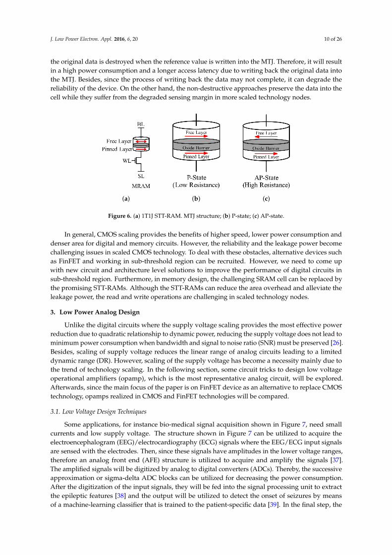
The STT-RAM is a promising candidate to replace the SRAM cells due to its unique featuresincluding non-volatility, low leakage, long endurance, CMOS-compatibility, and high-speed access [27].The STT-RAM cell consists of a Magnetic Tunnel Junction (MTJ) in series with an access transistor,which is controlled by the WL signal. The MTJ is composed of two magnetic layers, i.e., pinned layerand free layer, and one oxide barrier layer as shown in Figure 6. MTJ resistance is defined by therelative magnetization direction of two ferromagnetic layers. When the magnetization directions ofmagnetic layers are parallel (P-state) or anti-parallel (AP-state), MTJ resistance is in low or high states,respectively. Thus, the MTJ can be used as a binary memory cell (low resistance (RL): logic “0”—highresistance (RH): logic “1”). The process of parallelizing the free and pinned layers is more efficientthan the anti-parallelizing process. Besides, according to Figure 6a, write currents are significantlydifferent. When current flows from the bit-line (BL) to source-line (SL), the gate-source voltage of theaccess transistor is equal to VDD since the transistor source is grounded. It results in an overdrivevoltage of VDD-Vth. However, when the current flows from SL to BL, the overdrive voltage of thetransistor is considerably degraded because the MTJ functions as a source degeneration resistance inthis scenario. Furthermore, the body biasing effect increases the threshold voltage of the transistor andfurther degrades the write current.
The above described phenomena result in an asymmetric write operation in the STT-MRAM cell.The write operation is also a stochastic process and altered during time, even when the operating andenvironmental conditions remain the same [27]. The switching possibility is improved by extendingthe write pulse period (i.e., duration of write current), hence the write failure probability is reduced.On the other hand, increasing the switching current can decrease both mean and variation of theswitching time, which also helps to reduce write failures. However, this approach occupies a largerdie area in an STT-MRAM cell, decreasing the memory density. In order to solve this issue, severalassist techniques have been proposed to reduce the write time and power consumption. For example,in [28], a negative voltage is applied to the BL during write “1” operation to improve the drivability ofthe access transistor. Furthermore, in [29], an external magnetic field is applied to MTJ to facilitate theswitching process leading to the critical current reduction. Other methods have been proposed whichmonitor the data in the cell and terminate the write operation immediately after switching [30–33].However, all these assist methods improve the switching process at the expense of extended areaoverhead and/or reliability problem.
At sub-22 nm technologies, the performance and reliability of the STT-RAMs during read becomeschallenging. In scaled technology nodes, read disturbances increase mainly due to the scaling of thecritical current, IC. The read disturbance of the STT-RAMs is caused by the same current paths for readand write. The read current should be sufficiently lower than IC to avoid any disturbance during readoperation. Although a small read current alleviates the read disturbance, it will reduce the read margin,which considerably increases read failure probability. The read margin is defined as the differencebetween the BL voltage and reference voltage, and a good design with large read margin is requireddue to the small Tunneling Magnetoresistance Ratio (TMR) of the available MTJ technologies. To dealwith this issue, self-reference read scheme has been proposed, which compares the original resistancestate of the MTJ to a reference resistance provided by the same MTJ [34–36]. Such techniques can becategorized mainly into destructive and non-destructive sensing schemes. In destructive schemes,
J. Low Power Electron. Appl. 2016, 6, 20 10 of 26
the original data is destroyed when the reference value is written into the MTJ. Therefore, it will resultin a high power consumption and a longer access latency due to writing back the original data intothe MTJ. Besides, since the process of writing back the data may not complete, it can degrade thereliability of the device. On the other hand, the non-destructive approaches preserve the data into thecell while they suffer from the degraded sensing margin in more scaled technology nodes.
(a) (b) (c)
Figure 6. (a) 1T1J STT-RAM. MTJ structure; (b) P-state; (c) AP-state.
In general, CMOS scaling provides the benefits of higher speed, lower power consumption anddenser area for digital and memory circuits. However, the reliability and the leakage power becomechallenging issues in scaled CMOS technology. To deal with these obstacles, alternative devices suchas FinFET and working in sub-threshold region can be recruited. However, we need to come upwith new circuit and architecture level solutions to improve the performance of digital circuits insub-threshold region. Furthermore, in memory design, the challenging SRAM cell can be replaced bythe promising STT-RAMs. Although the STT-RAMs can reduce the area overhead and alleviate theleakage power, the read and write operations are challenging in scaled technology nodes.
3. Low Power Analog Design
Unlike the digital circuits where the supply voltage scaling provides the most effective powerreduction due to quadratic relationship to dynamic power, reducing the supply voltage does not lead tominimum power consumption when bandwidth and signal to noise ratio (SNR) must be preserved [26].Besides, scaling of supply voltage reduces the linear range of analog circuits leading to a limiteddynamic range (DR). However, scaling of the supply voltage has become a necessity mainly due tothe trend of technology scaling. In the following section, some circuit tricks to design low voltageoperational amplifiers (opamp), which is the most representative analog circuit, will be explored.Afterwards, since the main focus of the paper is on FinFET device as an alternative to replace CMOStechnology, opamps realized in CMOS and FinFET technologies will be compared.
3.1. Low Voltage Design Techniques
Some applications, for instance bio-medical signal acquisition shown in Figure 7, need smallcurrents and low supply voltage. The structure shown in Figure 7 can be utilized to acquire theelectroencephalogram (EEG)/electrocardiography (ECG) signals where the EEG/ECG input signalsare sensed with the electrodes. Then, since these signals have amplitudes in the lower voltage ranges,therefore an analog front end (AFE) structure is utilized to acquire and amplify the signals [37].The amplified signals will be digitized by analog to digital converters (ADCs). Thereby, the successiveapproximation or sigma-delta ADC blocks can be utilized for decreasing the power consumption.After the digitization of the input signals, they will be fed into the signal processing unit to extractthe epileptic features [38] and the output will be utilized to detect the onset of seizures by meansof a machine-learning classifier that is trained to the patient-specific data [39]. In the final step, the

J. Low Power Electron. Appl. 2016, 6, 20 11 of 26
outputs of the classifier (data) will be sent to an external device, such as a mobile phone or a server ina clinic [40].
Figure 7. Architecture of a bio-medical signal acquisition system.
In [41], a typical wireless EEG system is described. In this system, first, 18 channels are utilizedfor EEG signals recording and amplification. Then, after the digitization of the amplified EEG signals,the feature vector extraction is done locally and only the classification is performed remotely. Finally,the radio frequency transmitter used in this system is a commercially available low-power transmitter,ChipCon CC2550 [42]. As a result, by considering the actual measurements of the hardware prototypefor 18 channels, the total power consumption of this system is about 120 µW .
At low supply voltages, scaling of threshold voltage can be considered as an alternative to improvethe DR. However, similar to the digital case, the lower Vth reduces the noise margin and hence degradesSNR. On the other hand, many design techniques have been proposed for low voltage analog circuitswhich provide an acceptable noise and bandwidth specifications [43–46]. In low supply voltages,the analog circuits can be implemented in the sub-threshold region [43,44,47–49]. By considering thesub-threshold region, the drain-source current and transconductance equations are obtained as thefollowing equations [26]:
ID = ID0WL
eVGSnVT
(1− e
−VDSVT
). (2)
gm =∂ID
∂VGS=
IDnVT
, (3)
where n > 1 is a nonideality factor and VT = kT/q is the thermal voltage. From Equation (3), it canbe seen that the transconductance in the sub-threshold region is larger than the corresponding insaturation region (gm = 2ID/(VGS − Vth)) mainly due to the exponential dependence of the draincurrent on VGS in the sub-threshold region. However, in the sub-threshold region, the bandwidthis limited. Therefore, using of the sub-threshold region is suitable for the applications in which thecrucial specification is the power consumption not the speed.
By scaling the technology, the output impedence of the device is shrinking mainly due to channellength modulation. One solution is to cascade several low gain stages, but the stability problemwill be aggravated. Therefore, in high gain opamp structures, the cascaded transistors at the outputstages are utilized to increase the output impedance. However, due to the threshold voltages of thecascaded transistors, this structure cannot be utilized for low voltage regime. To deal with this obstacle,the self-cascode structure can be used in which the high output impedance is achieved in the lowvoltage design. As shown in Figure 8a, a self-cascode structure is a 2-transistor structure in whichboth of the transistors have the same gate bias voltages and the size of M2 is considered k times largerthan the size of M1 [44]. Figure 8b shows the current mirror structure based on self-cascode MOSFETs.

J. Low Power Electron. Appl. 2016, 6, 20 12 of 26
As depicted, M1 and M2 has the same DC current, but since the size of M2 is k times larger than M1,the overdrive voltage of M1 and the output voltage will be:
Voverdrive,M1 =(√
k− 1)
Voverdrive,M2, (4)
Voutput =(√
k)
Voverdrive,M1. (5)
(a) (b)
Figure 8. (a) Self-cascode structure; (b) A current mirror structure based on self-cascade MOSFETs.
According to Equations (4) and (5), for k > 1, the output voltage of the self-cascode structurehas increased. Therefore, the self-cascode structure can be realized at the output stage of theop-amps in order to increase the output impedance in low voltage regime. Many techniques havealso been proposed to settle challenging opamp designs in switched-capacitor circuits, which havegained importance in analog and mixed-signal designs. As mentioned earlier, low supply voltageleads to lower signal swing which requires a higher capacitance to maintain the same SNR bynoise improvement. Higher capacitance imposes more power dissipation to achieve the same speed.To address the challenges, attractive solutions such as correlated level shifting (CLS) [45] andComparator-Based (CB) opamps [46] have been proposed. In CLS, the error, emerging from finiteopamp gain, is alleviated by sampling the output signal during an estimation phase and then improvingthe output signal by removing the error signal. This technique can provide a rail-to-rail operationleading to a higher SNR. The CB structure replaces the opamp with a combination of a comparatorand current sources. This technique uses the fact that the opamp provides a virtual ground duringthe charge transfer phase in switched-capacitor circuits. Therefore, the comparator can be replacedto detect the virtual ground condition and enables the charge transfer phase. Both CLS and CBopamp structures can be utilized in low power high performance switched-capacitor analog andmixed-signal applications.
As mentioned above, CMOS circuits can be implemented in the sub-threshold region. For thesecircuits, the reference voltage decreases as well as the supply voltage that is reduced below thethreshold voltage [50,51]. Implementing CMOS circuits in subthreshold region requires designingaccurate voltage regulators as well. In literature, some works [52,53] have shown implementations ofvoltage references using MOSFETs operating in sub-threshold region. However, the main problemof these circuits is the variation of the reference voltage followed by process variations. Therefore,in [54,55], the resistive dividers are utilized to achieve the output voltage below the threshold voltage.But, lower currents require large resistors which enlarges the area. Recently, some voltage referencecircuits [56,57] have been implemented based on two devices with different threshold voltages. In thesecircuits, the output voltage is obtained according to the threshold voltage difference of two transistors.However, the process variation and the specific process technologies limit the use of these voltagereference circuits. In [58], another voltage reference circuit, based on the switched capacitor technology

J. Low Power Electron. Appl. 2016, 6, 20 13 of 26
and the body effect in MOSFETs, is introduced. In this circuit, the output voltage is obtained asthe difference between two gate-source voltages using only one PMOS transistor operated in thesub-threshold region. This reference voltage circuit has low sensitivity to the temperature andconsumes nano-power.
3.2. Analog Cells in FinFET Technology
As mentioned previously, the FinFET technology is currently utilized by digital designers forlow voltage and low area applications because of the superior energy efficiency with respect tostandard MOSFETs. Today, most electronic chips and circuit implementations include both digital andanalog structures in combination with each other. Therefore, using the FinFET technology for analogcircuits is essential as well, so the entire chip can be fabricated using the same technology.
Due to the better electrostatic characteristics of the FinFET, higher intrinsic gains are obtainedin more power efficient ways. However, the main challenges of the FinFET device are the higherparasitics derived from source resistances and extrinsic capacitors [59] and the quantified width ofthe device.
To evaluate the performance of the FinFET in analog designs, a two stage opamp structure,showed in Figrue 9, is designed in 14 nm FinFET and 65 nm CMOS technologies.
Figure 9. The two-stage opamp structure in 65 nm CMOS and 14 nm FinFET technologies.
It should be noted that the mentioned 65 nm CMOS technology is based on the TSMC PDK model.In this comparison, the different results of two technologies are obtained according to one specific goal.Therefore, the simulation results have been extracted based on the same phase margin of 60◦ and listedin Table 4. By this condition, the DC gain in 14 nm FinFET devices is 10 dB more than the DC gainin 65 nm CMOS technology. Also, the power consumption has been decreased from 416 µW in 65 nmCMOS technology to 180 µW in 14 nm FinFET technology, as was desired. Furthermore, as shownin Table 4, the unity gain bandwidth of the 14 nm FinFET technology (338 MHz) is higher than theunity gain bandwidth of the 65 nm CMOS technology (125 MHz). (It should be noted since the 16 nmCMOS technology is not available for us, we have compared the two analog circuits in the 14 nmFinFET and 65 nm CMOS technologies. But, since this 65 nm CMOS technology is based on the realTSMC PDK model, the obtained results are more accurate than the results achieved by comparingthe 14 nm FinFET technology and 16 nm CMOS technology which is not based on the real TSMCPDK model.)

J. Low Power Electron. Appl. 2016, 6, 20 14 of 26
Table 4. Two stage opamp in 14 nm FinFET and 65 nm CMOS technologies.
Parameter 14 nm 65 nm
DC Gain 51.9 dB 41.7 dBPhase Margin 60.3◦ 60◦
Unity gain bandwidth 338 MHz 125 MHzPower Consumption 180.93 µW 416 µW
Cc 200 fF 200 fFCload 500 fF 500 fF
The main features of implementing the radio frequency (RF) CMOS circuits such as low noiseamplifies (LNAs) are their gain, speed, power consumption and noise. As mentioned in [60],FinFET devices achieve higher gain in comparison with the planar CMOS devices. However,the specific speed ( fT) is higher in planar CMOS devices compared to the FinFET devices. Furthermore,as mentioned above, FinFET devices are very power-efficient in comparison with the planar devices.In addition to the gain, speed and the power performances of the RF design using planar andFinFET devices, noise is an important performance feature as well. As depicted in Figure 10 andmentioned in [58], the noise figure (NF) of the inductive LNAs is proportional to f0/ fT , where f0 is theoperating frequency. Furthermore, the NF of the feedback-based LNA is proportional to 1/gm [58].Finally, by considering the same current consumption for both FinFET and planar devices, it is evidentthat since the FinFET devices have higher parasitic capacitance derived from source resistances andextrinsic capacitors [59], the FinFET devices have lower fT and higher noise in comparison with theplanar devices. As a result, device optimization will be required to decrease the parasitics and improvethe performance of the FinFET devices for RF applications [61]. As an example described in [60],by consuming similar power (10 mA), the FinFET LNA devices achieve lower bandwidth (2 GHz) andhigher NF because of their higher parasitics in comparison with the planar devices with a bandwidthof 2.5 GHz, and a low NF of 2.6 dB. In summary, although the planar devices provide lower gain incomparison with the FinFET devices, their speed and noise performances are more appropriate forRF applications.
(a) (b)
Figure 10. Circuit schematics of (a) the inductive LNA; and (b) the feedback-based LNA.
4. Energy Harvesting
Reducing the energy cost of running an electronic system can enable us to use energy harvestingas a power source. This opens up for a whole range of new applications both in terms of distributedwireless networks in rough environments, where it is not possible to access the sensor node by wiresor change batteries, or in implanted sensors where size and bio compatible requirements makes itimpossible to attach a battery. Instead, different energy harvesting techniques makes it possible toharvest ambient energy from the surroundings and continuously power the system.

J. Low Power Electron. Appl. 2016, 6, 20 15 of 26
In this section, we will look at the feasibility of powering a system using only energy harvestingtechniques and discuss the advantages and disadvantages of some of the more popular methods andcertain combinations of harvesters.
4.1. Techniques and Sources
There are a variety of energy sources available in the environment such as light from the sun orindoor lighting, electromagnetic waves from cell phones and WiFi connections, vibrational energy fromengines and buildings, wind power, wave energy, waste heat etc. The human body is, in itself, also anincredible source of power, both in terms of mechanical movement and vibrations when we move ortalk, continuous stream of blood flow, excess heat, bio-chemical energy from physiological processes,etc. All these power sources can be harvested by kinetic harvesters, fuel cells, solar cells and thermalharvesters. The kinetic harvesters are mainly comprised of piezo electric and troboelectric harvesters,electrostatic transduction and magnetic induction generators. A good review of the most popularharvesting techniques was done by J. Olivo et al. [62]. It was found that the power income of harvesterswas: kinetic; 40 µW–80 µW, thermoelectric; 1 µW–30 µW, fuel cells; 2 µW–430 µW and inductive links;0.14 mW–150 mW, respectively.
4.1.1. Solar Energy
Solar energy is an abundantly available and exploitable energy source outside and has beenthoroughly researched for decades in the pursuit of producing even higher energy conversionefficiencies. Solar cells have developed into 5 main categories, crystalline silicon, thin film cells,organic/polymer, hybrid PV cells and dye-sensitized cells to fit a variety of applications, ranging frombig solar power plants to small wearable devices. Crystalline silicon is one of the original cell typesand is advantageous because of the easy availability and good efficiency (21%–28%) [63]. However,the manufacturing costs are significant, so cheaper alternatives, such as thin film cells, where lessmaterial is needed, are explored. Thin film cells come in a range of different technologies (amorphous,CdS/CdTe, CIS/CIGS) [64], with efficiencies ranging from 11%–29% [63], with the lowest efficiencybeing the recently emerging quantum dot technology. In 2014, a new efficiency record at 46.5% of amulti-junction concentrator solar cell, was presented by Tibbits et al. [65]. However, the usefulness ofthis multi-junction type is limited by the high fabrication cost and, for some applications, the inflexiblestructure. In stead, organic cells and dye sensitized cells are showing great potential because of thelow fabrication cost and for the organic cells; low environmental impact, wide tunability of chemicalfunctionalities and good compatibility with flexible substrates that makes them a great candidatefor wearable/implanted devices. The maximum lab efficiencies ranges from 5%–11.5% with thebest performance given by the dye sensitized [63,66–68]. A more detailed overview of the top labefficiencies is provided by NREL [63] (National Renewable Energy Laboratory (NREL) www.nrel.gov).
With a typical spectral irradiance of 1000 W/m2 on a surface illuminated by the sun at theAM1.5 standard, the power produced by the solar cells in the efficiency range of 5%–45% is5 mW/cm2–45 mW/cm2. If the device is operating indoor, the spectral irradiance depends on the lightsource and the solar cell efficiencies also depend on how the bandgap energies match the light source.However, a typical range of irradiation is 0.05 mW/cm2–5 mW/cm2 [69] and if we consider theworst case scenario, the corresponding converted power outputs in the same efficiency range are2.5 µW/cm2–22.5 µW/cm2.
An example of an autonomous bio implant that is powered solely by solar energy is an implantableintra ocular pressure monitor done by Ghaed et al. [70] in 2013. The low power techniques utilized areultra high threshold voltage and thick gate oxide to keep the leakage power low in the capacitance todigital converter. The SRAM is a 10T cell that uses gate length biasing in the dataretaining portionwhile power gating the read buffer to acheive 2.4 fW/bit standby leakage [71]. The VDD is scaled downclose to the minimum energy point so the micro processor and SRAM consume only 90 nW combinedat 0.45 V in active mode. The entire system including a capacitive MEMS pressure sensor, capacitance

J. Low Power Electron. Appl. 2016, 6, 20 16 of 26
to digital converter, transceiver, SRAM, µP and SCVR is powered by a 0.07 mm2 solar cell that producesbetween 13 nW and 80 nW in bright indoor and outdoor sunny lighting respectively. This correspondsto a power output of 0.02 mW/cm2–0.11 mW/cm2, which is significantly less outdoor than what isstated above, however, it must be noted that this system is implanted in the eye and therefore neversubjected to direct sunlight and significant absorption of some wavelengths is expected. The system isnevertheless able to measure the intra ocular pressure every 15 min and transmit the data once a daywith only 1.5 h of sunlight or 10 h of indoor lighting per day.
4.1.2. Mechanical Energy
Mechanical energy is the most widely distributed energy source and it is a source that fits wellwith the area of IoT that includes human-related motion applications. An extensively researchedtechnique to harvest mechanical energy, is using piezoelectric and triboelectric materials because of thepossible applications in flexible and wearable electronics. Other techniques such as magnetic inductionor electrostatic transduction have also been used extensively in the past, however, with the recent trendin comfortable, flexible and compact wearable devices, the piezoelectric and triboelectric materialsshow most potential in flexible materials that are functional, cheap and easily industrially available.
The most common materials used are ZnO, lead zirconate titanate (PZT), poly (vinylidenefluoride) (PVDF), 2D materials and composite materials. PZT is a widely used ceramic materialwith high dielectric constant and piezoelectric voltage, but it is also brittle and can only withstanda maximum safe strain of 0.2% [72]. Generators such as piezoelectric nanogenerators (PENGs) andflexible triboelectric nanogenerators (TENGs) have been extensively researched since the first ZnOnanowire-based generator was demonstrated in 2006 [73]. TENGs are simple and cost effectiveand the maximum power output of a triboelectric nano-generator has reached 50 mW/cm2 [74]and an energy conversion efficiency of 70.6% [75]. This means that it can also be used to harvestenergy on a large scale, like wave or wind energy. However, a typical flexible polymer TENGfor wearable applications yields a power density of 10.4 µW/cm3 [72]. For biological applications,the polymer-based piezoelectric materials, PVDF, is advantageous because of the chemical resistanceof polymers, the ease of fabrication, flexibility and bio-compatibility. The disadvantage is that in orderto achieve good performance, the material must be electrically poled first [72].
In order to track and convert motion energy from humans without the uncomfortable feeling ofhaving to bend something when you move, piezoelectric fibers have been developed [76]. They haveproven to be bent and folded repeatedly without any damage and they can produce an output powerof 60 nW at 1.5 V with a bending frequency of 2 Hz. Furthermore, arrays of these fibres have excellentpressure response at small values (0.1 Pa at low pressures) so they can work excellently as pressuresensors. For smart clothing application, fibers have been coated with nanowires by Lee et al. andwoven to a fabric using the “brush-to-brush” fabrication model, where the nano wires brush up anddown against each other and generates electricity from slow movements (<1 Hz). This results in apower density of 16 µW/cm2 [77].
Implanted sensors and actuators powered by piezoelectric materials can also be realized bypowering them externally using ultrasonic waves. This power transfer option is often the better choicewhen dealing with very small and deeply implanted sensors. In Figure 11, an overview of poweroutputs from RF, near-field (typically inductive) and ultrasonic sources is shown. The figure shows thegeneral trend that RF is relatively low power outputs and best for near-surface implants, near-fieldgives high power outputs for near-surface implants, but is relatively large and ultrasound gives highpower outputs even for deeply implanted small sensors.

J. Low Power Electron. Appl. 2016, 6, 20 17 of 26
10 -2
10 -1
20
10 0
10 1
10 2
15 40
Pow
erou
tput
/mW
Receiver size /mm Implant Depth /cm
205 100 0
Chen et al. 2007 [78]Arsalan et al. 2013 [79]
Moradi et al. 2013 [80]
Ahn and Ghovanloo 2016 [81]
Sauer et al. 2004 [82]
Parramon et al. 1997 [83]
O’Driscoll et al. 2009 [84]
Kim et al. 2015 [85]
Tsai et al. 2011 [86]
Song et al. 2015 [87]
Charthad et
Christensen and Roundy 2015[88]
Larson and Towe 2011 [89]
Maleki et al. 2011 [90]
al. 2015 [91]
3010
Figure 11. Comparison between RF (red), Near-field (pink) and ultrasound energy harvesting (blue) inimplantable devices.
When implanted sensors and actuators are powered externally using ultrasonic waves,the pressure wave from the ultrasound will force the piezoelectric material to stretch and compressand an AC current will be produced. An example of a device, powered by ultrasonic energy transfer,was demonstrated by Charthad et al. 2015 [91]. The device is a 4 mm× 7.8 mm implant includingan IC with a 2 nF on-chip storage capacitor, a hybrid data link consisting of a ultrasonic downlink andRF uplink. The system can support a load of 100 µW and the total power consumption of the IC is85 µW, which is far more than the previous example of a solar powered implant, however, by usingultrasonic power, the available power is also much higher. The system is powered at a distance of 3 cmin chicken meat by a 0.36 mW/mm2 ultrasonic wave, which is 5% of the FDA limit. The dimensions ofthe ultrasound piezoelectric receiver is 1 mm× 1 mm× 1.4 mm.
4.1.3. Combinations of Energy Harvesters
A combination of energy harvesters can be useful for cases where multiple energy sources canprovide a comparable amount of energy to boost the total harvested power. It can also be advisablewhen the harvesting circuits requires initial power to harvest energy. This is, for instance, the casefor highly efficient solar harvesters where the energy must be harvested at a specific voltage foroptimum efficiency.
Flexible hybrid nano-generators (FHNGs) have been developed to harvest multiple types ofenergy sources that complements each other in an effective manner. The challenge here is to choosesuitable materials with good flexibility, compatibility and mechanical stability and develop fabricationmethods that are applicable to the industry.
An example of a FHNG with harvesters that complements each other is the combination of PENGand TENG by Jung et al. [92]. Here, the high piezoelectric current output and the high triboelectricoutput voltage is powering simultaneously in one operating cycle. The combination produces a peak

J. Low Power Electron. Appl. 2016, 6, 20 18 of 26
voltage of 370 V, a current density of 12 µA/cm2 and a power density of 2.04 mW/cm3. The devicecan successfully power 600 LEDs by the force of fingers (≈0.2 N).
Because the voltage level of indoor operated solar cells becomes comparable to PENGsvoltage output, it is also a good design to use both PENGs and solar cells together. A combination ofan organic solar cell in co-junction with a ZnO piezoelectric material is developed by [93]. The deviceis a combination of several flexible layers, including Indium tin oxide as cathode for the solar cell,and the average power conversion efficiency of the solar cell was 1.5% with an open circuit voltage andcurrent density of 0.55 V and 9.2 mA/cm2 in standard AM 1.5 illumination respectively. However, theindoor photovoltaic voltages ranged from 10 mV to ≈ 120 mV which fits well with the piezoelectricvoltage that was up to 150 mV and an output current around hundreds of nA [93].
Even a triple combination of a thermal, solar and mechanical energy harvesters have beenfabricated by Yang et al. [94].
4.2. Energy Harvesting Interfaces
When designing an energy harvesting system (see Figure 12), the transducer (energy harvestingunit) is usually not suitable to power the loads directly because of the often low input voltageand varying nature of the ambient energy sources and thus the power input level. Therefore theenergy is transferred directly to a power converter that upconverts the voltage to the desired leveland then charges the energy storage or buffer that powers the load. Architectures have also beenmade where a control system directs the power directly to the load, bypassing the energy storage,when there is enough ambient energy, thus saving energy by not having to charge and discharge theenergy to the storage unit [95]. The energy storage is usually implemented using super-capacitors(or ultra-capacitors) because of the longer life time compared to conventional batteries. Even thoughthey have lower energy density than batteries, the power density is larger and they have a practicallyunlimited number of recharge cycles.
The control unit has the crucial task of keeping the power converter operating at the most energyefficient level both taking the maximum power point (MPP) of the transducer and the charge levelof the energy storage into account. For transducers such as solar cells, the MPP is greatly dependenton the illumination and the input impedance of the power converter must therefore be matched withthe optimum current output of the solar cell by utilizing a tracking scheme that follows the powerinput from the cell. However, internally, the power converter must also be regulated to balanceconduction loss, switching loss and charge redistribution loss based on the amount of charge that mustbe transferred and the voltage and charge level of the energy storage.
Figure 12. Block diagram of an energy harvesting system.
In order to improve the efficiency of an energy harvesting system, it is not enough to improvethe efficiency of the individual blocks because that might degrade the overall efficiency since they alloperate interactively. It can therefore be very time consuming to optimize an ultra low power energy

J. Low Power Electron. Appl. 2016, 6, 20 19 of 26
harvesting system, however, time can be saved by implementing all but the block in question as e.g.,a Verilog model to speed up the simulation process.
Power Converters
Power converters are an absolute necessity in mm-size energy harvesting systems.Power converters have been extensively researched in battery-powered embedded systems, however,the optimization objective is very different in energy harvesting systems so a complete reuse of thosesystems would lead to a degradation of performance [96].
For RF energy, triboelectric and piezoelectric energy receivers, it is necessary to use anAC/DC rectifier. Figure 13a shows a conventional multistage diode structure on which an analyticalmodel for optimization was developed [97]. This design was further optimized in 2016 for ultra lowpower purposes with a PCE of 72% for 19 µW load [98]. In 2014, an improved a switched-offset biasingscheme was proposed by compensating for the delays of the active diodes, which could otherwisecause reverse leakage current [99]. They reached power conversion efficiencies between 82% and 90%.Later, [100] proposed an active recitifier where switching loss and conduction loss have been balancedby setting the on-time and off-time calibrations to the near optimum value. They reached a peak PCEof 94.8%.
Solar cells and thermoelectric harvesters produce DC currents, so only DC/DC buck/boostconverters are necessary here. There are two main categories of charge pumps, the inductor basedand the switched capacitor based. For low power densities (<1 mW/mm2) capacitor based CPsare more efficient, however, for higher power densities, and applications with larger area, bulkyinductors is usually the better option [101]. The first capacitive charge pump proposed was the Dicksoncharge pump, and since a variety of improved linear charge pumps have been developed. However,the performance of linear charge pumps degrades significantly in ultra low voltage transducers.Therefore the charge transfer capability was subsequently improved by designing a tree topologycharge pump [102]. Cross-coupled switched capacitor voltage doublers (see Figure 13b) are alsowell suited for low input voltage applications, however, when the input voltage drops below thethreshold voltage, the charge pump malfunctions. Therefore, a further improvement of the crosscoupled charge pump was proposed by using an auxilliary negative charge pump to enable lowerinput voltages and utilizing dynamic body bias and adaptive dead-time to increase the PCE [103].A theoretical study of the design considerations has been carried out for several types of charge pumpsby Ki et al. [104].
(a) (b)
Figure 13. (a) Multistage AC/DC rectifier; (b) cross coupled capacitive charge pump.
4.3. Sustainable Operation Using Ambient Energy
When you look at the power consumption of different block in a mm-scale wireless device,you will most often find that the most power consuming part, by far, is the RF transmitter. However,in many applications it is not necessary to transmit more than a few bytes each hour, which makes

J. Low Power Electron. Appl. 2016, 6, 20 20 of 26
the average energy consumption comparable with the rest of the circuit blocks. For these cases,currently, energy harvesting techniques are able to power systems with only basic functionalities,however, a further decrease of power consumption from analog and digital circuits would providemore sophisticated implants with increased computation power. A continuous downscaling ofthe technology furthermore decreases the environmental impact of sensors when embedded incomplex systems, such as the human body. This paves the way for more intelligent implants,drug delivery systems, neuro implants and other medical advances.
In general, the best form of energy harvesting depends on the application; in cases where thesystem requires a long lifetime and is remote or otherwise inaccessible, e.g., distributed wildlife/forestfire sensors, or you just have no desire to power the system by any form of power transfer, e.g.,smart clothes, tents, backpacks, etc., a solar powered system is advantageous. However, if theapplication is a relatively deep or size restricted implant that requires high stability, ultrasonic poweris the better choice, although if the implant is placed near a “power source” such as blood/air flowor heartbeats, piezoelectric nanogenerators are coming up as viable alternatives. For top skin/fatlayer applications with no significant size restrictions, other types of near-field energy sources canbe considered. However, note that when the transfer medium is air, RF is advised, but if it is metal,again ultrasound is a good option. In cases where the environment is rich on specific chemicals thatcan power a fuel cell, this is a cheap, environmentally friendly but time limited solution, that doesn’trequire external power. Finally, devices that are situated in highly vibrating/moving environments,e.g., engines, shoes, wristwatches, etc., kinetic harvesters like piezoelectric, triboelectric, magneticinduction or electrostatic transduction can be used.
5. Conclusions
In this paper, design challenges in integrated circuit design for future battery-less WIDswere explained. Furthermore, some proposed techniques were introduced to tackle such challengesfrom device to circuit and architecture level. All in all, battery-less WIDs will not be possible withoutintroducing novel technologies such as FinFET etc. as replica for CMOS technology as well as circuitand architecture techniques to lower the power consumption significantly due to the lack of enoughavailable energy from harvesters. On the other side, combining different harvesting techniques in acompact way will be the solution to generate more power to such WIDs. Therefore, we envision moreresearch on combined energy harvesting technologies along with device circuit co-design techniquesas an enabling solution for future battery-less WIDs.
Author Contributions: Katrine Lundager is the main author and thus responsible for writing the paper. Shehas contributed with Section 4 about energy harvesting, Behzad Zeinali has been responsible for the digital andmemory sections of the paper (Section 2), Mohammed Tohidi has been responsible for the analog part (Section 3)and Jens K. Madsen and Farshad Moradi have been responsible for revising and supervising the paper.
Conflicts of Interest: The authors declare no conflict of interest.
Abbreviations
The following abbreviations are used in this manuscript:

J. Low Power Electron. Appl. 2016, 6, 20 21 of 26
WID Wearable/Implantable DeviceTEG Thermoelectric GeneratorIC Integrated CircuitSoC System-on-ChipSCE Short Channel EffectRF Radio frequencyIoT Internet of ThingsIoBNT Internet of Bio-Nano ThingsMuGFET Multi-Gate Field-Effect TransistorCNT-FET Carbon Nanotube Field-Effect TransistorRDF Random Dopant FluctuationEOT Equivalent Gate Dielectric Thickness
PTM Predective Technology ModelDIBL Drain Induced Barrier LoweringSS Sub-threshold SwingSRAM Static Random Access MemoryWL Word-lineBL Bit-lineSL Source-lineRBL Read Bit-lineRWL Read Word-lineRWLC Read Word-line ComplementaryCS Column SelectEN Enable SignalRSNM Read Static Noise MarginWM Write MarginSA Sense AmplifierSTT-RAM Spin Transfer Torque Random Access MemoryMTJ Magnetic Tunnel JunctionSNR Signal-to-Noise RatioDR Dynamic RangeOPAMP Operational AmplifierEEG ElectroencephalogramECG ElectrocardiographyADC Analog-to-Digital ConverterAFE Analog Front-EndCLS Correlated Level ShiftingCB Comparator BasedNREL National Renewable Energy LaboratorySCVR Switched Capacitor Voltage RegulatorPZT Lead Zirconate TitanateUS UltrasonicPENG Piezoelectric Nano-GeneratorTENG Triboelectric Nano-GeneratorPV PhotovoltaicCIGS Copper Indium Gallium SelenideAM Air MassMEMS Microelectromechanical SystemFHNG Flexible Hybrid Nanogenerator
References
1. Pal, A. Low-Power VLSI Circuits and Systems; Springer: New Delhi, India, 2014.

J. Low Power Electron. Appl. 2016, 6, 20 22 of 26
2. Akyildiz, I.F.; Pierobon, M.; Balasubramaniam, S.; Koucheryavy, Y. The internet of Bio-Nano things.IEEE Commun. Mag. 2015, 53, 32–40.
3. Pedram, M. Power Minimization in IC Design: Principles and Applications. ACM Trans. Des. Autom.Electron. Syst. 1996, 1, 3–56.
4. Chandrakasan, A.P.; Sheng, S.; Brodersen, R.W. Low-power CMOS digital design. IEEE J. Solid-State Circuits1992, 27, 473–484.
5. Athas, W.C.; Svensson, L.J.; Koller, J.G.; Tzartzanis, N.; Chou, E.Y.C. Low-power digital systems based onadiabatic-switching principles. IEEE Trans. Very Large Scale Integr. (VLSI) Syst. 1994, 2, 398–407.
6. Wuytack, S.; Catthoor, F.; Franssen, F.; Nachtergaele, L.; De Man, H. Global communication and memoryoptimizing transformations for low power systems. In Proceedings of the IEEE International Workshop onLow Power Design, Napa Valley, CA, USA, 24–27 April 1994; pp. 203–208.
7. Tiwari, V.; Malik, S.; Wolfe, A. Power analysis of embedded software: A first step towards software powerminimization. IEEE Trans. Very Large Scale Integr. (VLSI) Syst. 1994, 2, 437–445.
8. Collaert, N.; Keersgieter, A.D.; Dixit, A.; Ferain, I.; Lai, L.S.; Lenoble, D.; Mercha, A.; Nackaerts, A.;Pawlak, B.J.; Rooyackers, R.; et al. Multi-gate devices for the 32 nm technology node and beyond.In Proceedings of the 37th European Solid State Device Research Conference, Muenchen, Germany,11–13 September 2007; pp. 143–146.
9. Noda, K.; Tatsumi, T.; Uchida, T.; Nakajima, K.; Miyamoto, H.; Hu, C. A 0.1-µm delta-doped MOSFETfabricated with post-low-energy implanting selective epitaxy. IEEE Trans. Electron Devices 1998, 45, 809–814.
10. Yan, R.H.; Ourmazd, A.; Lee, K.F. Scaling the Si MOSFET: From bulk to SOI to bulk. IEEE Trans.Electron Devices 1992, 39, 1704–1710.
11. Sachid, A.B.; Hu, C. Denser and More Stable SRAM Using FinFETs With Multiple Fin Heights. IEEE Trans.Electron Devices 2012, 59, 2037–2041.
12. Tawfik, S.A.; Kursun, V. Multi-Threshold Voltage FinFET Sequential Circuits. IEEE Trans. Very Large ScaleIntegr. (VLSI) Syst. 2011, 19, 151–156.
13. Moradi, F.; Gupta, S.K.; Panagopoulos, G.; Wisland, D.T.; Mahmoodi, H.; Roy, K. Asymmetrically DopedFinFETs for Low-Power Robust SRAMs. IEEE Trans. Electron Devices 2011, 58, 4241–4249.
14. Predictive Technology Model (PTM). Available online: http://ptm.asu.edu (accessed on 17 October 2016).15. Lin, C.H.; Haensch, W.; Oldiges, P.; Wang, H.; Williams, R.; Chang, J.; Guillorn, M.; Bryant, A.; Yamashita, T.;
Standaert, T.; et al. Modeling of width-quantization-induced variations in logic FinFETs for 22 nm andbeyond. In Proceedings of the Symposium on VLSI Technology (VLSIT), Kyoto, Japan, 14–16 June 2011;pp. 16–17.
16. Gu, J.; Keane, J.; Sapatnekar, S.; Kim, C. Width Quantization Aware FinFET Circuit Design. In Proceedingsof the IEEE Custom Integrated Circuits Conference, San Jose, CA, USA, 10–13 September 2006; pp. 337–340.
17. Hsieh, C.Y.; Fan, M.L.; Hu, V.P.H.; Su, P.; Chuang, C.T. Independently-Controlled-Gate FinFET SchmittTrigger Sub-Threshold SRAMs. IEEE Trans. Very Large Scale Integr. (VLSI) Syst. 2012, 20, 1201–1210.
18. Liu, Z.; Tawfik, S.A.; Kursun, V. An independent-gate FinFET SRAM cell for high data stability andenhanced integration density. In Proceedings of the IEEE International SOC Conference, Hsin Chu, Taiwan,26–29 September 2007; pp. 63–66.
19. Kim, Y.B.; Kim, Y.B.; Lombardi, F. Low power 8T SRAM using 32 nm independent gate FinFET technology.In Proceedings of the IEEE International SOC Conference, Newport Beach, CA, USA, 17–20 September 2008;pp. 247–250.
20. Chen, Y.H.; Chan, W.M.; Wu, W.C.; Liao, H.J.; Pan, K.H.; Liaw, J.J.; Chung, T.H.; Li, Q.; Lin, C.Y.;Chiang, M.C.; et al. A 16 nm 128 Mb SRAM in High-κ Metal-Gate FinFET Technology with Write-AssistCircuitry for Low-VMIN Applications. IEEE J. Solid-State Circuits 2015, 50, 170–177.
21. Karl, E.; Wang, Y.; Ng, Y.G.; Guo, Z.; Hamzaoglu, F.; Meterelliyoz, M.; Keane, J.; Bhattacharya, U.; Zhang, K.;Mistry, K.; et al. A 4.6 GHz 162 Mb SRAM Design in 22 nm Tri-Gate CMOS Technology with IntegratedRead and Write Assist Circuitry. IEEE J. Solid-State Circuits 2013, 48, 150–158.
22. Lien, N.C.; Chu, L.W.; Chen, C.H.; Yang, H.I.; Tu, M.H.; Kan, P.S.; Hu, Y.J.; Chuang, C.T.; Jou, S.J.; Hwang, W.A 40 nm 512 kb Cross-Point 8 T Pipeline SRAM with Binary Word-Line Boosting Control, Ripple Bit-Lineand Adaptive Data-Aware Write-Assist. IEEE Trans. Circuits Syst. I Regul. Pap. 2014, 61, 3416–3425.
J. Low Power Electron. Appl. 2016, 6, 20 23 of 26
23. Raychowdhury, A.; Geuskens, B.; Kulkarni, J.; Tschanz, J.; Bowman, K.; Karnik, T.; Lu, S.L.; De, V.;Khellah, M.M. PVT-and-aging adaptive wordline boosting for 8T SRAM power reduction. In Proceedings ofthe IEEE International Solid-State Circuits Conference (ISSCC), Francisco, CA, USA, 7–11 February 2010;pp. 352–353.
24. Verma, N.; Chandrakasan, A.P. A 256 kb 65 nm 8T Subthreshold SRAM Employing Sense-AmplifierRedundancy. IEEE J. Solid-State Circuits 2008, 43, 141–149.
25. Zeinali, B.; Madsen, J.K.; Raghavan, P.; Moradi, F. Sub-Threshold SRAM Design in 14 Nm FinFET Technologywith Improved Access Time and Leakage Power. In Proceedings of the IEEE Computer Society AnnualSymposium on VLSI, Montpellier, France, 8–10 July 2015; pp. 74–79.
26. Rajput, S.S.; Jamuar, S.S. Low voltage analog circuit design techniques. IEEE Circuits Syst. Mag. 2002,2, 24–42.
27. Huai, Y. Spin-transfer torque MRAM (STT-MRAM): Challenges and prospects. AAPPS Bull. 2008, 18, 33–40.28. Farkhani, H.; Peiravi, A.; Moradi, F. Low-Energy Write Operation for 1T-1MTJ STT-RAM Bitcells with
Negative Bitline Technique. IEEE Trans. Very Large Scale Integr. (VLSI) Syst. 2016, 24, 1593–1597.29. Fong, X.; Kim, Y.; Choday, S.H.; Roy, K. Failure Mitigation Techniques for 1T-1MTJ Spin-Transfer Torque
MRAM Bit-cells. IEEE Trans. Very Large Scale Integr. (VLSI) Syst. 2014, 22, 384–395.30. Zheng, T.; Park, J.; Orshansky, M.; Erez, M. Variable-energy write STT-RAM architecture with bit-wise
write-completion monitoring. In Proceedings of the IEEE International Symposium on Low PowerElectronics and Design (ISLPED), Beijing, China, 4–6 September 2013; pp. 229–234.
31. Bi, X.; Sun, Z.; Li, H.; Wu, W. Probabilistic design methodology to improve run-time stability andperformance of STT-RAM caches. In Proceedings of the IEEE/ACM International Conference onComputer-Aided Design (ICCAD), 5–8 November 2012; pp. 88–94.
32. Zhou, P.; Zhao, B.; Yang, J.; Zhang, Y. Energy reduction for STT-RAM using early write termination.In Proceedings of the IEEE/ACM International Conference on Computer-Aided Design—Digest of TechnicalPapers, Prague, Czech Republic, 11–14 October 2009; pp. 264–268.
33. Bishnoi, R.; Ebrahimi, M.; Oboril, F.; Tahoori, M.B. Asynchronous Asymmetrical Write Termination (AAWT)for a low power STT-MRAM. In Proceedings of the Design, Automation Test in Europe Conference Exhibition(DATE), Dresden, Germany, 24–28 March 2014.
34. Jeong, G.; Cho, W.; Ahn, S.; Jeong, H.; Koh, G.; Hwang, Y.; Kim, K. A 0.24-µm 2.0-V 1T1MTJ 16-kb nonvolatilemagnetoresistance RAM with self-reference sensing scheme. IEEE J. Solid-State Circuits 2003, 38, 1906–1910.
35. Chen, Y.; Li, H.; Wang, X.; Zhu, W.; Xu, W.; Zhang, T. A 130 nm 1.2 V/3.3 V 16 Kb Spin-Transfer TorqueRandom Access Memory With Nondestructive Self-Reference Sensing Scheme. IEEE J. Solid-State Circuits2012, 47, 560–573.
36. Motaman, S.; Ghosh, S.; Kulkarni, J.P. A novel slope detection technique for robust STTRAM sensing.In Proceedings of the IEEE/ACM International Symposium on Low Power Electronics and Design (ISLPED),Rome, Italy, 22–24 July 2015; pp. 7–12.
37. Chen, W.M.; Chiueh, H.; Chen, T.J.; Ho, C.L.; Jeng, C.; Ker, M.D.; Lin, C.Y.; Huang, Y.C.; Chou, C.W.;Fan, T.Y.; et al. A Fully Integrated 8-Channel Closed-Loop Neural-Prosthetic CMOS SoC for Real-TimeEpileptic Seizure Control. IEEE J. Solid-State Circuits 2014, 49, 232–247.
38. Yoo, J.; Yan, L.; El-Damak, D.; Altaf, M.A.B.; Shoeb, A.H.; Chandrakasan, A.P. An 8-Channel ScalableEEG Acquisition SoC With Patient-Specific Seizure Classification and Recording Processor. IEEE J.Solid-State Circuits 2013, 48, 214–228.
39. Altaf, M.A.B.; Tillak, J.; Kifle, Y.; Yoo, J. A 1.83 µJ/classification nonlinear support-vector-machine-basedpatient-specific seizure classification SoC. In Proceedings of the IEEE International Solid-State CircuitsConference Digest of Technical Papers, San Francisco, CA, USA, 17–21 February 2013; pp. 100–101.
40. Cao, T.V.; Maier, C.; Wisland, D.; Lande, T.S.; Cauwenberghs, G. BFSK MICS direct-DCO transmitterwith adaptive background frequency regulation. In Proceedings of the 38th European Solid State CircuitsConference (ESSCIRC), Bordeaux, France, 17–21 September 2012; pp. 305–308.
41. Verma, N.; Shoeb, A.; Bohorquez, J.; Dawson, J.; Guttag, J.; Chandrakasan, A.P. A Micro-Power EEGAcquisition SoC With Integrated Feature Extraction Processor for a Chronic Seizure Detection System.IEEE J. Solid-State Circuits 2010, 45, 804–816.
42. Low-Cost Low-Power 2.4 GHz RF Transmitter. Available online: http://focus.ti.com/docs/prod/folders/print/cc2550.html (accessed on 17 October 2016).

J. Low Power Electron. Appl. 2016, 6, 20 24 of 26
43. Ismail, M.; Fiez, T. Analog VLSI: Signal and Information Processing; Electronics and VLSI Circuits; McGraw-Hill:New York, NY, USA, 1994.
44. Rajput, S.S.; Jamuar, S.S. Low voltage analog circuit design techniques. IEEE Circuits and Systems Magazine2002, 2, 24–42.
45. Gregoire, B.R.; Moon, U.K. An Over-60 dB True Rail-to-Rail Performance Using Correlated Level Shiftingand an Opamp With Only 30 dB Loop Gain. IEEE J. Solid-State Circuits 2008, 43, 2620–2630.
46. Fiorenza, J.K.; Sepka, T.; Holloway, P.; Sodini, C.G.; Lee, H.S. Comparator-Based Switched-Capacitor Circuitsfor Scaled CMOS Technologies. IEEE J. Solid-State Circuits 2006, 41, 2658–2668.
47. Blalock, B.J.; Allen, P.E.; Rincon-Mora, G.A. Designing 1-V op amps using standard digital CMOS technology.IEEE Trans. Circuits Syst. II Analog Digit. Signal Process. 1998, 45, 769–780.
48. Rajput, S.S.; Jamuar, S.S. Design Techniques for Low Voltage Analog Circuit Structures. In Proceedings of the2001 IEEE National Symposium On Microelectronics, Genting Highlands, Malaysia, 12–13 November 2001.
49. Yan, S.; Sanchez-Siencio, E. Low Voltage Analog Circuit Design Techniques: A Tutorial. IEICE Trans. AnalogIntegr. Circuits Syst. 2000, 82, 179–195.
50. Hanson, S.; Zhai, B.; Seok, M.; Cline, B.; Zhou, K.; Singhal, M.; Minuth, M.; Olson, J.; Nazhandali, L.;Austin, T.; et al. Exploring Variability and Performance in a Sub-200-mV Processor. IEEE J. Solid-StateCircuits 2008, 43, 881–891.
51. Kim, T.H.; Liu, J.; Keane, J.; Kim, C.H. A 0.2 V, 480 kb Subthreshold SRAM with 1 k Cells per Bitline forUltra-Low-Voltage Computing. IEEE J. Solid-State Circuits 2008, 43, 518–529.
52. Ueno, K.; Hirose, T.; Asai, T.; Amemiya, Y. A 300 nW, 15 ppm/◦C, 20 ppm/V CMOS Voltage ReferenceCircuit Consisting of Subthreshold MOSFETs. IEEE J. Solid-State Circuits 2009, 44, 2047–2054.
53. Lee, J.; Cho, S. A 210 nW 29.3 ppm/◦C 0.7 V voltage reference with a temperature range of −50 to 130 ◦C in0.13 µm CMOS. In Proceedings of the Symposium on VLSI Circuits (VLSIC), Kyoto, Japan, 15–17 June 2011;pp. 278–279.
54. Giustolisi, G.; Palumbo, G.; Criscione, M.; Cutri, F. A low-voltage low-power voltage reference based onsubthreshold MOSFETs. IEEE J. Solid-State Circuits 2003, 38, 151–154.
55. Vita, G.D.; Iannaccone, G. An ultra-low-power, temperature compensated voltage reference generator.In Proceedings of the IEEE Custom Integrated Circuits Conference, San Jose, CA, USA, 18–21 September2005; pp. 751–754.
56. Magnelli, L.; Crupi, F.; Corsonello, P.; Pace, C.; Iannaccone, G. A 2.6 nW, 0.45 V Temperature-CompensatedSubthreshold CMOS Voltage Reference. IEEE J. Solid-State Circuits 2011, 46, 465–474.
57. Seok, M.; Kim, G.; Blaauw, D.; Sylvester, D. A Portable 2-Transistor Picowatt Temperature-CompensatedVoltage Reference Operating at 0.5 V. IEEE J. Solid-State Circuits 2012, 47, 2534–2545.
58. Zhang, H.; Huang, M.; Zhang, Y.; Li, X.; Yoshihara, T. A nano-power switched-capacitor voltage referenceusing body effect in MOSFETs for application in subthreshold LSI. In Proceedings of the IEEE InternationalConference of Electron Devices and Solid-State Circuits (EDSSC), Hong Kong, China, 3–5 June 2013.
59. Wambacq, P.; Verbruggen, B.; Scheir, K.; Borremans, J.; Heyn, V.D.; Plas, G.V.D.; Mercha, A.; Parvais, B.;Subramanian, V.; Jurczak, M.; et al. Analog and RF circuits in 45 nm CMOS and below: Planar bulk versusFinFET. In Proceedings of the 32nd European Solid-State Circuits Conference, Montreux, Switzerland,19–21 September 2006; pp. 54–57.
60. Borremans, J.; Parvais, B.; Dehan, M.; Thijs, S.; Wambacq, P.; Mercha, A.; Kuijk, M.; Carchon, G.; Decoutere, S.Perspective of RF design in future planar and FinFET CMOS. In Proceedings of the IEEE Radio FrequencyIntegrated Circuits Symposium, Atlanta, GA, USA, 15–17 June 2008; pp. 75–78.
61. Raskin, J.P.; Pailloncy, G.; Lederer, D.; Danneville, F.; Dambrine, G.; Decoutere, S.; Mercha, A.; Parvais, B.High-Frequency Noise Performance of 60-nm Gate-Length FinFETs. IEEE Trans. Electron Devices 2008,55, 2718–2727.
62. Olivo, J.; Carrara, S.; Micheli, G.D. Energy Harvesting and Remote Powering for Implantable Biosensors.IEEE Sens. J. 2011, 11, 1573–1586.
63. Best Research-Cell Efficiencies, NREL. Available online: http://www.nrel.gov/ncpv/images/efficiency_chart.jpg (accessed on 2 July 2016).
64. Pandey, A.; Tyagi, V.; Selvaraj, J.A.; Rahim, N.; Tyagi, S. Recent advances in solar photovoltaic systems foremerging trends and advanced applications. Renew. Sustain. Energy Rev. 2016, 53, 859–884.

J. Low Power Electron. Appl. 2016, 6, 20 25 of 26
65. Tibbits, T.N.D.; Beutel, P.; Grave, M.; Karcher, C.; Oliva, E.; Siefer, G.; Wekkeli, A.; Schachtner, M.; Dimroth, F.;Bett, A.W.; et al. New Efficiency Frontiers with Wafer-Bonded Multi-Junction Solar Cells. In Proceedingsof the 29th European PV Solar Energy Conference and Exhibition, Amsterdam, The Netherlands,22–26 September 2014.
66. Wang, Z.L.; Wu, W. Nanotechnology-Enabled Energy Harvesting for Self-Powered Micro-/Nanosystems.Angew. Chem. Int. Ed. 2012, 51, 11700–11721.
67. Mishra, A.; Bäuerle, P. Small Molecule Organic Semiconductors on the Move: Promises for Future SolarEnergy Technology. Angew. Chem. Int. Ed. 2012, 51, 2020–2067.
68. Li, G.; Zhu, R.; Yang, Y. Polymer solar cells. Nat. Photonics 2012, 6, 153–161.69. Virtuani, A.; Lotter, E.; Powalla, M. Performance of Cu(In,Ga)Se2 solar cells under low irradiance.
Thin Solid Films 2003, 431–432, 443–447.70. Chen, G.; Ghaed, H.; Haque, R.; Wieckowski, M.; Kim, Y.; Kim, G.; Fick, D.; Kim, D.; Seok, M.; Wise, K.; et al.
A cubic-millimeter energy-autonomous wireless intraocular pressure monitor. In Proceedings of the IEEEInternational Solid-State Circuits Conference, Francisco, CA, USA, 20–24 February 2011; pp. 310–312.
71. Kim, D.; Chen, G.; Fojtik, M.; Seok, M.; Blaauw, D.; Sylvester, D. A 1.85fW/bit ultra low leakage 10T SRAMwith speed compensation scheme. In Proceedings of the IEEE International Symposium of Circuits andSystems (ISCAS), Rio de Janeiro, Brazil, 15–18 May 2011; pp. 69–72.
72. Fan, F.R.; Tang, W.; Wang, Z.L. Flexible Nanogenerators for Energy Harvesting and Self-Powered Electronics.Adv. Mater. 2016, 28, 4283–4305.
73. Wang, Z.L.; Song, J. Piezoelectric Nanogenerators Based on Zinc Oxide Nanowire Arrays. Science 2006,312, 242–246.
74. Zhu, G.; Zhou, Y.S.; Bai, P.; Meng, X.S.; Jing, Q.; Chen, J.; Wang, Z.L. A Shape-Adaptive Thin-Film-BasedApproach for 50% High-Efficiency Energy Generation Through Micro-Grating Sliding Electrification.Adv. Mater. 2014, 26, 3788–3796.
75. Tang, W.; Jiang, T.; Fan, F.R.; Yu, A.F.; Zhang, C.; Cao, X.; Wang, Z.L. Liquid-Metal Electrode forHigh-Performance Triboelectric Nanogenerator at an Instantaneous Energy Conversion Efficiency of 70.6%.Adv. Funct. Mater. 2015, 25, 3718–3725.
76. Persano, L.; Dagdeviren, C.; Su, Y.; Zhang, Y.; Girardo, S.; Pisignano, D.; Huang, Y.;Rogers, J.A. High performance piezoelectric devices based on aligned arrays of nanofibers ofpoly(vinylidenefluoride-co-trifluoroethylene). Nat. Commun. 2013, 4, 1633.
77. Lee, M.; Chen, C.Y.; Wang, S.; Cha, S.N.; Park, Y.J.; Kim, J.M.; Chou, L.J.; Wang, Z.L. A Hybrid PiezoelectricStructure for Wearable Nanogenerators. Adv. Mater. 2012, 24, 1759–1764.
78. Chen, H.; Liu, M.; Jia, C.; Zhang, C.; Wang, Z. Low Power IC Design of the Wireless Monitoring System of theOrthopedic Implants. In Proceedings of the 29th Annual International Conference of the IEEE Engineeringin Medicine and Biology Society, Milano, Italy, 25–29 August 2007; pp. 5766–5769.
79. Arsalan, M.; Ouda, M.H.; Marnat, L.; Ahmad, T.J.; Shamim, A.; Salama, K.N. A 5.2 GHz, 0.5 mW RF poweredwireless sensor with dual on-chip antennas for implantable intraocular pressure monitoring. In Proceedingsof the IEEE MTT-S International Microwave Symposium Digest (IMS), Seattle, WA, USA, 2–7 June 2013.
80. Moradi, E.; Björninen, T.; Sydänheimo, L.; Ukkonen, L.; Rabaey, J.M. Analysis of wireless powering ofmm-size neural recording tags in RFID-inspired wireless brain-machine interface systems. In Proceedings ofthe IEEE International Conference on RFID, Orlando, FL, USA, 30 April–2 May 2013; pp. 8–15.
81. Ahn, D.; Ghovanloo, M. Optimal Design of Wireless Power Transmission Links for Millimeter-SizedBiomedical Implants. IEEE Trans. Biomed. Circuits Syst. 2016, 10, 125–137.
82. Sauer, C.; Stanacevic, M.; Cauwenberghs, G.; Thakor, N. Power harvesting and telemetry in CMOS forimplanted devices. In Proceedings of the IEEE International Workshop on Biomedical Circuits and Systems,Rotterdam, The Netherlands, 31 October–2 November 2004.
83. Parramon, J.; Doguet, P.; Marin, D.; Verleyssen, M.; Munoz, R.; Leija, L.; Valderrama, E. ASIC-basedbatteryless implantable telemetry microsystem for recording purposes. In Proceedings of the 19th AnnualInternational Conference of the IEEE Engineering in Medicine and Biology Society, Chicago, IL, USA,30 October–2 November 1997; Volume 5, pp. 2225–2228.
84. O’Driscoll, S.; Poon, A.S.Y.; Meng, T.H. A mm-sized implantable power receiver with adaptive linkcompensation. In Proceedings of the IEEE International Solid-State Circuits Conference—Digest of TechnicalPapers, San Francisco, CA, USA, 8–12 February 2009; pp. 294–295.

J. Low Power Electron. Appl. 2016, 6, 20 26 of 26
85. Kim, A.; Ochoa, M.; Rahimi, R.; Ziaie, B. New and Emerging Energy Sources for Implantable WirelessMicrodevices. IEEE Access 2015, 3, 89–98.
86. Tsai, J.Y.; Huang, K.H.; Wang, J.R.; Liu, S.I.; Li, P.C. Ultrasonic wireless power and data communication forneural stimulation. In Proceedings of the IEEE International Ultrasonics Symposium, Orlando, FL, USA,18–21 October 2011; pp. 1052–1055.
87. Song, S.H.; Kim, A.; Ziaie, B. Omnidirectional Ultrasonic Powering for Millimeter-Scale Implantable Devices.IEEE Trans. Biomed. Eng. 2015, 62, 2717–2723.
88. Christensen, D.B.; Roundy, S. Ultrasonically powered piezoelectric generators for bio-implantable sensors:Plate versus diaphragm. J. Intell. Mater. Syst. Struct. 2016, 27, 1092–1105.
89. Larson, P.J.; Towe, B.C. Miniature ultrasonically powered wireless nerve cuff stimulator. In Proceedings ofthe 5th International IEEE/EMBS Conference on Neural Engineering (NER), Cancun, Mexico, 27 April–1 May2011; pp. 265–268.
90. Maleki, T.; Cao, N.; Song, S.H.; Kao, C.; Ko, S.C.; Ziaie, B. An Ultrasonically Powered ImplantableMicro-Oxygen Generator (IMOG). IEEE Trans. Biomed. Eng. 2011, 58, 3104–3111.
91. Charthad, J.; Weber, M.J.; Chang, T.C.; Arbabian, A. A mm-Sized Implantable Medical Device (IMD)With Ultrasonic Power Transfer and a Hybrid Bi-Directional Data Link. IEEE J. Solid-State Circuits 2015,50, 1741–1753.
92. Jung, W.S.; Kang, M.G.; Moon, H.G.; Baek, S.H.; Yoon, S.J.; Wang, Z.L.; Kim, S.W.; Kang, C.Y. High OutputPiezo/Triboelectric Hybrid Generator. Sci. Rep. 2015, 5, doi:10.1038/srep09309.
93. Choi, D.; Lee, K.Y.; Jin, M.J.; Ihn, S.G.; Yun, S.; Bulliard, X.; Choi, W.; Lee, S.Y.; Kim, S.W.; Choi, J.Y.; et al.Control of naturally coupled piezoelectric and photovoltaic properties for multi-type energy scavengers.Energy Environ. Sci. 2011, 4, 4607–4613.
94. Yang, Y.; Zhang, H.; Zhu, G.; Lee, S.; Lin, Z.H.; Wang, Z.L. Flexible Hybrid Energy Cell for SimultaneouslyHarvesting Thermal, Mechanical, and Solar Energies. ACS Nano 2013, 7, 785–790.
95. Bandyopadhyay, S.; Chandrakasan, A.P. Platform Architecture for Solar, Thermal, and Vibration EnergyCombining with MPPT and Single Inductor. IEEE J. Solid-State Circuits 2012, 47, 2199–2215.
96. Lu, C.; Raghunathan, V.; Roy, K. Efficient Design of Micro-Scale Energy Harvesting Systems. IEEE J. Emerg.Sel. Top. Circuits Syst. 2011, 1, 254–266.
97. Yi, J.; Ki, W.H.; Tsui, C.Y. Analysis and Design Strategy of UHF Micro-Power CMOS Rectifiers forMicro-Sensor and RFID Applications. IEEE Trans. Circuits Syst. I Regul. Pap. 2007, 54, 153–166.
98. Haddad, P.A.; Gosset, G.; Raskin, J.P.; Flandre, D. Automated Design of a 13.56 MHz 19 µW Passive RectifierWith 72% Efficiency Under 10 µA load. IEEE J. Solid-State Circuits 2016, 51, 1290–1301.
99. Lu, Y.; Ki, W.H. A 13.56 MHz CMOS Active Rectifier With Switched-Offset and Compensated Biasing forBiomedical Wireless Power Transfer Systems. IEEE Trans. Biomed. Circuits Syst. 2014, 8, 334–344.
100. Huang, C.; Kawajiri, T.; Ishikuro, H. A Near-Optimum 13.56 MHz CMOS Active Rectifier With Circuit-DelayReal-Time Calibrations for High-Current Biomedical Implants. IEEE J. Solid-State Circuits 2016, 51, 1797–1809.
101. Steyaert, M.; van Roermund, A.; Baschirotto, A. Analog Circuit Design: Low Voltage Low Power; Short RangeWireless Front-Ends; Power Management and DC-DC; Springer: Dordrecht, The Netherlands, 2014.
102. Lu, C.; Park, S.P.; Raghunathan, V.; Roy, K. Efficient power conversion for ultra low voltage micro scaleenergy transducers. In Proceedings of the Design, Automation Test in Europe Conference Exhibition (DATE),Dresden, Germany, 8–12 March 2010; pp. 1602–1607.
103. Kim, J.; Mok, P.K.T.; Kim, C. A 0.15 V Input Energy Harvesting Charge Pump With Dynamic Body Biasingand Adaptive Dead-Time for Efficiency Improvement. IEEE J. Solid-State Circuits 2015, 50, 414–425.
104. Ki, W.H.; Lu, Y.; Su, F.; Tsui, C.Y. Design and analysis of on-chip charge pumps for micro-power energyharvesting applications. In Proceedings of the IEEE/IFIP 19th International Conference on VLSI andSystem-on-Chip, Hong Kong, China, 3–5 October 2011; pp. 374–379.
c© 2016 by the authors; licensee MDPI, Basel, Switzerland. This article is an open accessarticle distributed under the terms and conditions of the Creative Commons Attribution(CC-BY) license (http://creativecommons.org/licenses/by/4.0/).