low-power charge readout circuit for pixel-based lar time
TRANSCRIPT

Low-power Charge Readout Circuit for Pixel-based LAr Time Projection Chamber
Puyu Wang & Lixiong Du
The University of Pennsylvania MooreSchoolofElectricalEngineeringworkingwiththe
DepartmentofPhysicsandAstronomy Abstract——In this report, a novel readout circuit for pixel-based Deep Underground Neutrino Experiment is proposed. The proposed circuit can integrate and reset after a given amount of input charge collected by pixel. The reset time difference will be used to recover current waveform and particle trajectory. A 3-stage charge amplifier and Schmitt trigger are designed with TSMC 65nm process. An ideal current pulse input with variable amplitude is used to mimic the arrival of ionization signal onto the pixel. The desired count of unit charge can be achieved under -40°C simulation, with static power of 50uW. 1. Introduction The Deep Underground Neutrino Experiment (DUNE) has been designed to explore the behavior of several families of neutrinos. Since they have no electric charge they escape direct detection except when they interact with matter. The dune experiment will look for evidence of neutrinos by detecting the sudden motion of charged particles within several large containers housing thousands of tons of liquid Argon chilled to -186°C. Details of the planned detector and scientific objectives can be found at http://www.dunescience.org/ Dr. David Nygren, previous lab director of Lawrence Berkeley Laboratory and inventor of the time projection chamber detector has proposed a simple approach that would consist of tiling the walls of the liquid Argon detectors with millions of 4mm x 4mm pixels that would reside in the cold. He proposed a simple, very low power, front-end electronics pixel readout approach designed to minimize the output information to keep power and infrastructure as small a feasible. This independent study will focus on the design of a multi-channel prototype charge amplifier and comparator circuit to help understand the feasibility of his suggested approach. The pixel readout circuits would operate at -186°C, with power consumption less than 100uW. Integration of unit charge is 1.32fC. It is estimated that the time to collect the charge for each count is several tens of milliseconds. Since the counter must be reset after generating a unit charge signal to be ready for additional charge it should be designed lose only minimal amounts of charge during reset. Another concern is the efficiency for multiple hits (linearity). TSMC 65nm process is currently used for simulation in Cadence. The proposed prototype circuit has included a layout with extracted R and C simulation results.
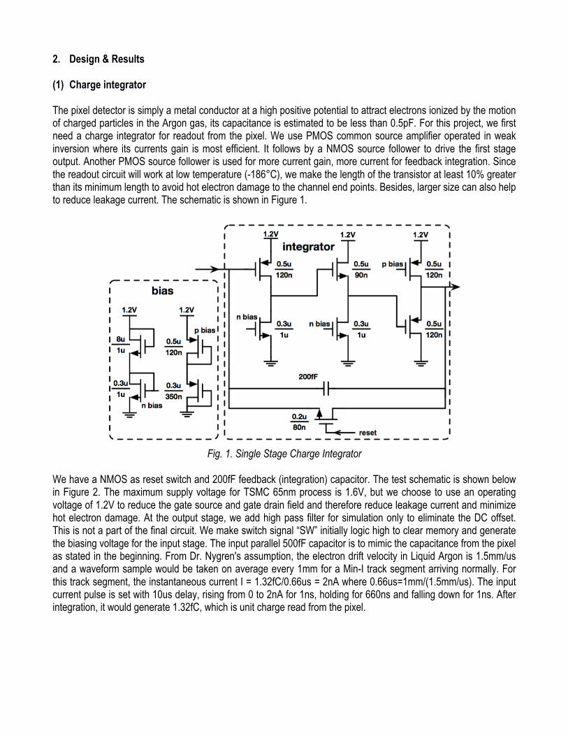
2. Design & Results (1) Charge integrator The pixel detector is simply a metal conductor at a high positive potential to attract electrons ionized by the motion of charged particles in the Argon gas, its capacitance is estimated to be less than 0.5pF. For this project, we first need a charge integrator for readout from the pixel. We use PMOS common source amplifier operated in weak inversion where its currents gain is most efficient. It follows by a NMOS source follower to drive the first stage output. Another PMOS source follower is used for more current gain, more current for feedback integration. Since the readout circuit will work at low temperature (-186°C), we make the length of the transistor at least 10% greater than its minimum length to avoid hot electron damage to the channel end points. Besides, larger size can also help to reduce leakage current. The schematic is shown in Figure 1.
Fig. 1. Single Stage Charge Integrator
We have a NMOS as reset switch and 200fF feedback (integration) capacitor. The test schematic is shown below in Figure 2. The maximum supply voltage for TSMC 65nm process is 1.6V, but we choose to use an operating voltage of 1.2V to reduce the gate source and gate drain field and therefore reduce leakage current and minimize hot electron damage. At the output stage, we add high pass filter for simulation only to eliminate the DC offset. This is not a part of the final circuit. We make switch signal “SW” initially logic high to clear memory and generate the biasing voltage for the input stage. The input parallel 500fF capacitor is to mimic the capacitance from the pixel as stated in the beginning. From Dr. Nygren's assumption, the electron drift velocity in Liquid Argon is 1.5mm/us and a waveform sample would be taken on average every 1mm for a Min-I track segment arriving normally. For this track segment, the instantaneous current I = 1.32fC/0.66us = 2nA where 0.66us=1mm/(1.5mm/us). The input current pulse is set with 10us delay, rising from 0 to 2nA for 1ns, holding for 660ns and falling down for 1ns. After integration, it would generate 1.32fC, which is unit charge read from the pixel.

Fig. 2. Test schematic for single stage charge integrator
For testing environment, the PDK models are only valid down to -40°C. Therefore, we will mainly focus on -40°C performance. Figure 3 and 4 present the simulation results from Cadence. The AC output generates roughly 5.3mV voltage after integrating 1.32fC charge. The current flowing through integrator is 10.6uA. Then power would be about 13uW. We need to cascade more stages to get enough voltage difference for the comparator.
Fig. 3 Input signal and control signal waveform Fig. 4. Simulation of single stage design
By cascading three stages of charge integrator, the schematic is shown in Figure 5. AC coupling capacitor is applied when connecting each stage together.
Fig. 5. Cascaded stages and test schematic
0 5 10 15 200
0.5
1
1.5
Cont
rol v
olta
ge (V
) NMOS switch control signal
0 5 10 15 20Time (us)
0
0.5
1
1.5
2
Inpu
t cur
rent
pul
se (n
A) Input current pulse
0 5 10 15 20Time (us)
-1
0
1
2
3
4
5
6
AC
out
put (
mV)
AC output after single stage
X: 11.45Y: 5.364
Simulation only AC Test Point
2pF Intra Stage Coupling Cap

The reason for making 2pF as connection capacitor is due to the linearity of the amplification. Parametric analysis is performed for linearity of amplification under different inter capacitance in Figure 6. It can be clearly seen that the inter stage capacitance quickly saturates above 10pF.
Fig. 6. Inter capacitor effect on charge integrator
Figure 7, 8 show the simulation results for cascaded 3-stage charge integrator. We get 164mV voltage difference for the final AC output.
Fig. 7. Charge integrator output for single hit Fig. 8. Test results for each stage of integrator
Moving on, we test how temperature affects the performance of this integrator. It seems to have larger voltage difference with higher temperature. But higher temperature also leads to larger leakage current, which might cause significant problem for our integrator.
0 5 10 15 20Time (us)
-30
-25
-20
-15
-10
-5
0
5
AC
out
put (
mV)
Second stage AC output
capacitance from0.2pF to 2pFstep size = 0.2pF
0 5 10 15 20 25 30Time (us)
-60
-50
-40
-30
-20
-10
0
10
AC
out
put (
mV)
Second stage AC output
capacitance from 2pF to 20pFstep size = 2pF
0 5 10 15 20Time (us)
-50
0
50
100
150
200
AC
out
put (
mV)
AC output after three stages
X: 11.5Y: 164
0 5 10 15 20Time (us)
-50
0
50
100
150
200
AC
out
put (
mV)
AC output
AC out1AC out2AC out3
X: 11.5Y: 164
X: 11.1Y: 5.36
X: 11.5Y: -28.1

Fig. 9. Output waveforms for different temperature
Besides, we check multiple current pulses which lead to the same charge integration of 1.32fC. The final output voltage is similar as single current pulse, both of which is 164mV/1.32fC. The result is shown below in Figure 10.
Fig. 10. Simulation results of two hits Fig. 11. AC output for different input current
While the intended prototype integrator amplifier needs only to register a single 1.32fC hit to record a count before being reset, we explored the linearity in the range where we intend to use it to be sure that it isn’t near saturation. In terms of linearity of the integrator, normal instantaneous current input is 2nA for 660ns. We make parametric analysis varying the magnitude from 1nA to 3nA with 0.5nA step size. The linearity is good under 3nA input current as shown in Figure 11. (2) Schmitt trigger The Schmitt trigger consists of a comparator and positive hysteresis feedback. For the comparator, we start with a differential input to single ended structure. The simulated DC gain is about 20dB. Usually, it follows by common source amplifier to increase gain. However, we only care more about the gain near the switching point of the comparator. An inverter could achieve this goal with less power consumption. Figure 12 shows the schematic.
0 5 10 15 20Time (us)
-50
0
50
100
150
200A
C o
utpu
t (m
V)Temperature dependence
-40°C-20°C0°C20°C40°C
9.5 10 10.5 11 11.5 12 12.5 13Time (us)
158
160
162
164
166
168
170
172
174
AC
out
put (
mV)
Temperature dependence
-40°C-20°C0°C20°C40°C
0 5 10 15 20Time (us)
-50
0
50
100
150
200
AC
out
put (
mV)
AC output after three stages
X: 11.46Y: 164
0 5 10 15 20Time (us)
-50
0
50
100
150
200
250A
C o
utpu
t (m
V)Linearity for input pulse
1nA1.5nA2nA2.5nA3nA

Fig. 12. Comparator schematic
The output after the third stage of charge integrator is about 808mV. To test the comparator, we make the negative input of comparator to be 800mV, and positive input is switching from 808mV to 850mV DC voltage plus a 5KHz AC Sin wave.
Fig. 13. Comparator test schematic
The simulation result of the comparator is shown below. We can see that the gain at 808mV is about 47dB. The power consumption of this comparator about 5uW.

Fig. 14. Test results of comparator
The schematic and testing are shown in Figure 15 and 16. The reason we choose inverter + positive feedback instead of direct positive feedback connection is to avoid feedback effects from output to the analog input. The feedback capacitor is used to tune the pulse width of the reset signal, and from simulation 3pF can generate a 180ns reset pulse width.
Fig. 15. Test schematic of Schmitt trigger

Fig. 16. Simulation results of Schmitt trigger
(3) Clock setting To avoid charge missing during reset, we need another control signal to disconnect the current flowing to the charge integrator during reset. It should be an inverting signal of reset, RESETBAR. And it’s supposed to go low before reset goes high and go high after reset goes low so that the charge could be stored on the pixel cap temporally and then pump the charge to the readout circuit after reset is finished. Figure 17 shows the schematic for non-overlapping clock generating, where resistor is used to add time constant between two clocks.
Fig. 17. Non-overlapping clock schematic

(4) Final design and simulation
Fig. 18. Block diagram
Our final schematic is shown below. All three charge integrators are included in single block. We need initial kick to provide operation point for the charge amplifier, i.e. reset and RESETBAR signal need to be high at the very beginning to set operating points. We design some logic gates to fulfill the goal. Another drain-source connected NMOS controlled by reset signal is used for charge compensation.
Fig. 19. Final design schematic
Currently we are using ideal current pulses for the simulation. But the real input waveform depends on both the number and angle of the particle trajectory. For example, if the particle trajectory is in parallel with readout pixel, the ionization electrons collected by pixel would cause the maximum current with relatively smaller pulse width for unit charge count. Figure 20 shows s simple sketch for the particle detector.

Fig. 20. Electrons collection with different trajectory angle
For the simulation, three test cases are applied to see the performance: 1nA for 40us, 2nA for 20us and 4nA for 10us. with the same amount of charge, 40fC. Since 1.32fC is single unit charge, 40fC would give about 30 reset counts in total. Following figures represent the simulation results of these cases. The "input" signal means the voltage across the pixel cap and the "reset" signal refers to the output of the comparator for switching.
Fig. 21. Simulation results for 1nA_40us input current

Fig. 22. Simulation results for 2nA_20us input current
Fig. 23. Simulation results for 4nA_10us input current
Input Expected count Simulation result
1nA for 40us 30 32 2nA for 20us 30 31 4nA for 10us 30 30
Table 1. Comparison table of schematic simulation
As input current increases and pulse width decreases, the number of reset signal would decrease a little bit. Since we don’t have real input signal imported to our simulation, we cannot conclude if the proposed circuit would operate correctly in real life. Besides, the total static power consumption is about 50uW. And the average power is about 56.4uW. Figure 24 shows the simulation results of current from power supply.
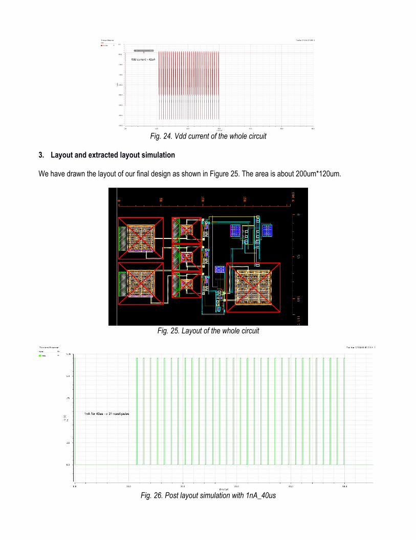
Fig. 24. Vdd current of the whole circuit
3. Layout and extracted layout simulation We have drawn the layout of our final design as shown in Figure 25. The area is about 200um*120um.
Fig. 25. Layout of the whole circuit
Fig. 26. Post layout simulation with 1nA_40us

Fig. 27. Post layout simulation with 2nA_20us
Fig. 28. Post layout simulation with 4nA_10us
Input Expected count Simulation result
1nA for 40us 30 31 2nA for 20us 30 30 4nA for 10us 30 29
Table 2. Comparison table of post layout simulation

4. Improvement (1) Dark current and operation point We give no input to measure the dark current. From Figure 29, every 410us the circuit would reset for a given 1.32fC unit charge. Therefore, the average dark current could be estimated as about 3pA. Even though it’s pretty small, it would change the operation point of charge amplifier, and then cause inaccurate reference voltage. Because threshold voltage is calculated based on the operation point. This may cause missing or additional charge for readout.
Fig. 29. Dark Current measurement
(2) Process variation We have not run Monte Carlo simulation for process variation. Since the components are quite small, the simulated result would be quite sensitive. (3) Performance of large input charge We have checked the circuit linearity performance with 1nA, 2nA and 4nA input. From Nygren’s assumption, the maximum current input could be 5 times the normal current, 2nA case. Giving a 4us 10nA current pulse which has the total amount charge of 40fC for 30 reset counts, we only get 19 counts of reset pulses. After plotting the waveform of Schmitt trigger, we find that negative input switches too slow during the falling edge when reset signal is logic low. Hence upper threshold voltage (~850mV) is far more than the target value (~800mV).

Fig. 30. Schmitt trigger simulation results with 10nA input
To solve this problem, we add a switch controlled by “sw” signal to short the resistor during the charge integration phase, which will make the falling edge switch faster. The adjusted schematic is shown below.
Fig. 31. Updated Schmitt trigger
The comparison simulation results are shown in Figure 32. The top one is the previous simulation result with threshold voltage around 850mV. The bottom one is updated version with threshold voltage be about 810mV.

Fig. 32. Comparison of Schmitt trigger simulation results with 10nA input
We update the layout with this new approach. And we simulate the performance with different current input ramping from 2nA to 10nA for same amount of time, 4us. In this way, we should get an arithmetic sequence for the number of reset pulse. The simulation results are shown in Figure 33.
Fig. 33. Ramping current input simulation results
The following Table 3 is to summarize the simulation results with extracted layout.
Input Expected counts Simulation results 2nA 6 6 4nA 12 11 6nA 18 17 8nA 24 21
10nA 30 26 Table 3. Comparison table with fixed duration, increasing input current pulses

To solve this problem, we go back to check the linearity of charge integrator. We inject a small amount of charge (100ns with different current input) to simulate AC output of the charge integrator. The results are shown in Figure 34. For 2nA 100ns input current pulse, the output increases 24mV. Ideally, for 10nA 100ns input current pulse, the output should have increase of 24mV*5=120mV. However, it only increases 110mV in the simulation. The absolute error is about 9%.
Fig. 34. Charge integrator with ramping current inputs
To solve this problem, we make the inter-stage coupling capacitor from 2pF to 1.7pF to have better linearity performance but will trade gain.
Fig. 35. Updated Charge integrator

Re-run the simulation and get the following result.
Fig. 36. Updated Charge integrator with ramping current inputs
The error is reduced to less than 3%, which will help larger input current performance. Since the gain is smaller than previous design, the hysteresis resistor and reference are tuned to get the right operation point. We simulate with different current input ramping from 2nA to 10nA for same amount of time (4us) as before and get the following results.
Fig. 37. Updated Schmitt Trigger

Fig. 38. Reset pulse waveform for different current input
Table 4 summarizes the final simulation results. This is the best simulation result in the schematic level.
Input Expected counts Simulation results 2nA 6 6 4nA 12 12 6nA 18 18 8nA 24 24
10nA 30 29 Table 4. Comparison table of final simulation results
5. Conclusion This study has proposed pixel-based readout circuit for a Liquid Argon Time Projection Chamber by combining charge integrator and Schmitt trigger using the TSMC 65nm process. By integrating units of equal charge marked by reset pulses sent off detector, this low power circuit is suitable for an arrayed detector to cover a wall of time projection chamber filled with a noble liquid gas such as Liquid Argon. Counting pulses registered by individual pixels created by a track and recording the pulse rate the position and extent of a charged particle track can be re-constructed by off line data acquisition. Our system can achieve good linearity of reset counts with input current ranging from 2nA to 10nA, with average power consumption 54uW. After drawing the layout, the reset counts of extracted layout simulation are close to expected number. We have achieved the goal in the proposal of the independent study, and we would like to thank Mitch Newcomer and Firooz Afatouni for discussions and improvement on the design. We hope this study can influence the future development of liquid noble gas detectors.