low-noise cold-field emission current obtained between two
TRANSCRIPT

HAL Id: hal-01430586https://hal.archives-ouvertes.fr/hal-01430586v2
Submitted on 23 Feb 2018
HAL is a multi-disciplinary open accessarchive for the deposit and dissemination of sci-entific research documents, whether they are pub-lished or not. The documents may come fromteaching and research institutions in France orabroad, or from public or private research centers.
L’archive ouverte pluridisciplinaire HAL, estdestinée au dépôt et à la diffusion de documentsscientifiques de niveau recherche, publiés ou non,émanant des établissements d’enseignement et derecherche français ou étrangers, des laboratoirespublics ou privés.
Low-noise cold-field emission current obtained betweentwo opposed carbon cone nanotips during in situ
transmission electron microscope biasingLudvig de Knoop, Christophe Gatel, Florent Houdellier, Marc Monthioux,
Aurélien Masseboeuf, Martin Hÿtch, Etienne Snoeck
To cite this version:Ludvig de Knoop, Christophe Gatel, Florent Houdellier, Marc Monthioux, Aurélien Masseboeuf, et al..Low-noise cold-field emission current obtained between two opposed carbon cone nanotips during insitu transmission electron microscope biasing. Applied Physics Letters, American Institute of Physics,2015, 106 (26), pp.263101. �10.1063/1.4923245�. �hal-01430586v2�

Low-noise cold-field emission current obtained between two opposed carbon conenanotips during in situ transmission electron microscope biasingL. de Knoop, C. Gatel, F. Houdellier, M. Monthioux, A. Masseboeuf, E. Snoeck, and M. J. Hÿtch
Citation: Appl. Phys. Lett. 106, 263101 (2015); doi: 10.1063/1.4923245View online: https://doi.org/10.1063/1.4923245View Table of Contents: http://aip.scitation.org/toc/apl/106/26Published by the American Institute of Physics
Articles you may be interested in Development of an ultrafast electron source based on a cold-field emission gun for ultrafast coherent TEMApplied Physics Letters 111, 023101 (2017); 10.1063/1.4991681
Transmission type flat-panel X-ray source using ZnO nanowire field emittersApplied Physics Letters 107, 243105 (2015); 10.1063/1.4938006
Temporal field emission current stability and fluctuations from graphene filmsApplied Physics Letters 97, 062106 (2010); 10.1063/1.3474800
Field emission properties of carbon nanotubesJournal of Vacuum Science & Technology B: Microelectronics and Nanometer Structures Processing,Measurement, and Phenomena 18, 665 (2000); 10.1116/1.591258
Field electron emission from pencil-drawn cold cathodesApplied Physics Letters 108, 193112 (2016); 10.1063/1.4949563
Low p-type contact resistance by field-emission tunneling in highly Mg-doped GaNApplied Physics Letters 109, 252101 (2016); 10.1063/1.4972408
Low-noise cold-field emission current obtained between two opposedcarbon cone nanotips during in situ transmission electron microscopebiasing
L. de Knoop, C. Gatel, F. Houdellier, M. Monthioux, A. Masseboeuf, E. Snoeck,and M. J. H€ytchCEMES, UPR-8011 CNRS, University of Toulouse, 29 rue Jeanne Marvig, 31055 Toulouse, France
(Received 9 April 2015; accepted 18 June 2015; published online 29 June 2015)
A dedicated transmission electron microscope sample holder has been used to study in situ the
cold-field emission process of carbon cone nanotips (CCnTs). We show that when using a CCnT
instead of a Au plate-anode, the standard deviation of the emission current noise can be decreased
from the 10 nA range to the 1 nA range under vacuum conditions of 10�5 Pa. This shows the strong
influence of the anode on the cold-field emission current noise. VC 2015 AIP Publishing LLC.
[http://dx.doi.org/10.1063/1.4923245]
In an electron gun, the electron emission process can be
either thermionic or field emission or a mix of both. Room
temperature field emission, commonly named cold-field
emission (CFE), is the brightest source available and also
exhibits the smallest energy spread.1 The reduced brightness
of commercially available CFE guns (CFEGs) is in the range
of 108 A m�2 Sr�1 V�1. This value needs to be compared
with the 105 A m�2 Sr�1 V�1 measured in a standard thermi-
onic gun. Furthermore, the energy spread can be up to 10
times smaller with a CFEG compared with a thermionic
gun.1
However, the CFEG suffers from two well-known draw-
backs. First, the emission and the corresponding probe cur-
rent noise remain high compared to a thermally-assisted
source. This is mainly due to not only ion bombardment of
the tip but also from atom migration across the cathode sur-
face (known as flicker noise).2 Second, probe and emission
current decrease over time with a continuous slope of
between 10% and 20% per hour. This phenomenon is mainly
due to the build-up of contamination on the emitter surface
that disturbs the emission process. The corresponding slope
in other electron sources is less than 1% per hour.3
To improve the properties of a CFE electron source,
experimentations have been made to exchange the standard
W emitter tip with, e.g., multi-wall carbon nanotubes
(CNTs)4–8 (or carbon onions welded onto a W tip9). Due to
the high aspect ratio and small tip radius of the structure, the
electric field is strongly enhanced. Therefore, the extraction
voltage for which the cold-field emission starts is smaller. The
small tip radius increases the associated brightness of the
source.7 Carbon is also chemically less reactive than W,
which reduces the contamination layer build-up on the sur-
face, ideally resulting in lower noise and better current stabil-
ity over time.10 Finally, the CNT high mechanical strength
decreases the chance of structural failure that can arise from
the extreme current density at the apex of the tip during field
emission.6 Despite these superior properties, the continuation
towards a commercial product has proven to be difficult. The
reasons for this could be that the inherent high aspect ratio of
CNTs causes them to vibrate upon electron emission, which
degrades the emission properties like the brightness11 (unless
they are shortened11,12). Additionally, due to their nm size,
CNTs are difficult to handle, which makes the process of
mounting time-consuming and unreliable.
We have earlier reported an alternative graphene-based
carbon structure, the carbon cone nanotip (CCnT), which
potentially could be implemented as a functional and easily
installable cathode emitter in a CFE gun.13 The CCnT com-
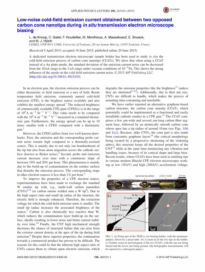
prises a few lm-wide and several lm-long carbon fiber seg-
ment base, followed by an atomically smooth carbon cone
whose apex has a tip radius of around 10 nm (see Figs. 1(b)
and 1(c)). Because, alike CNTs, the cone part is also made
from concentric graphene layers14 (the conical morphology
being created by a progressive shortening of the widening
tubes), this structure keeps all the desired properties of the
CNT13 while at the same time minimizing any vibration and
handling issues, because of its conical shape and large base.
Recent results, where CCnTs have been used as emitting tips
in various modern Hitachi CFE electron microscopes work-
ing at low (30 kV) and high (200 kV) acceleration voltage,
FIG. 1. (a) Front part of the TEM in situ biasing holder, with the nanomani-
pulator, driven by a piezo-tube. (b) A zoom-in of the two tips in the holder.
(c) Further zoom-in and hologram of the two CCnTs, with the top one being
biased and the lower one being ground. (the holographic measurements will
be reported in a subsequent paper.)
0003-6951/2015/106(26)/263101/4/$30.00 VC 2015 AIP Publishing LLC106, 263101-1
APPLIED PHYSICS LETTERS 106, 263101 (2015)

have revealed an unprecedented stability with almost no cur-
rent decay during one hour.15
In situ transmission electron microscope (TEM) biasing
experiments have also been performed to determine the
CCnT exit work function.16 This was carried-out in a speci-
alized TEM sample-biasing holder (see Fig. 1(a)) which
enabled to field-emit electrons inside the sample holder
while simultaneously observe and determine the electric field
around the apex, using a combination of electron hologra-
phy, the Fowler-Nordheim equations, and finite element
method modeling.16
Around the sample holder inside the TEM column, where
both experiments took place, the vacuum is in the order of
10�5 Pa, whereas inside a CFE source it is around 10�9 Pa in
order to maximize the current stability and minimize the noise.
Indeed, a higher vacuum pressure, as well as a higher current,
increases the noise and the current decay (as was reported by
Todokoro et al.2). Therefore, the noise level on the ieV-curves
measured during in situ field emission was high.
In this paper, we have performed the same experimental
setup as in the paper mentioned above,16 but using another
CCnT as anode instead of a Au plate. We will show how this
new configuration dramatically decreases the noise level of
the emission current.
The sample preparation was carried out using a Cross
Beam XB 1540 (Zeiss) focused ion-beam scanning electron
microscope equipped with a gas-injection system and a
microtweezer (Kleindiek) to manipulate the CCnTs.15
Electro-chemically etched W-tips were cut using the ion
beam and a Pt-precursor of the gas-injection system was
used to weld the CCnTs to the flattened W-tip apices (see
Fig. 1(b)). The two CCnTs of this experiment had similar tip
radii (5–10 nm) to the one used in the previous experiment.16
Furthermore, in both experiments, the vacuum was in the
order of 10�5 Pa. The CCnTs were inserted into a double-tilt
in situ biasing TEM holder (Nanofactory Instruments) that
allowed a potential of 6140 V to be applied between the
tips. A piezo-driven nanomanipulator allowed a long-range
and precise positioning of the CCnTs inside the TEM (Fig.
1(a)).17 The separation distance between the two CCnTs was
220 nm, whereas for the previous experiment, the distance
between the CCnT and the plate-Au anode was 3.5 lm.
Electron holograms were obtained using the SACTEM-
Toulouse, an image-corrected (CEOS) Tecnai F20 (FEI)
with a rotatable biprism and Schottky FEG. Phase analysis
of the holograms will be reported in a different paper.
Due to the high vacuum pressure, ieV-curves obtained
under the same conditions can differ significantly. So in
order to be able to quantitatively compare the noise level,
numerous current as a function of voltage (ieV)-curves were
obtained. The noise was calculated based on these using the
standard deviation, defined as below
r ¼
ffiffiffiffiffiffiffiffiffiffiffiffiffiffiffiffiffiffiffiffiffiffiffiffiPie � �ieð Þ2
n
s; (1)
where ie is the field-emission current that is measured in the
sample holder (see Fig. 1(c)), �ie ¼ ðP
ieÞ=n is the average
current, and n is the number of data points. Here, we
calculated r for 6 data points, which corresponded to an
increase of the potential of around 0.1 V. This was done from
60 to 400 nA on the ieV-curves. The ieV-curves differed
somewhat in resolution for data points per volt and a larger
voltage-span means a larger current-span and thus a higher
value of r. So in order to be able to compare r for different
ieV-curves, the slope, which can be assumed to be linear dur-
ing the 0.1 V increase, was removed using linear regression
analysis.
For each bundle of 6 data points, the linear regression
analysis resulted in an equation of the form f ðxÞ ¼ axþ b,
which describes the slope over this area. To obtain the stand-
ard deviation, b is not needed. For a, the following formula
was exploited:
a ¼ nP
Vieð Þ �P
VP
ie
nP
V2 �P
Vð Þ2;
where V is the applied potential and as before, n ¼ 6. Having
a, the linear slopes could be subtracted in order to obtain hor-
izontal data slopes and then the standard deviation values
were determined using Eq. (1). The linear regression analysis
also provided quantitative data of the noise level since r was
calculated on a non-inclined slope. For each ieV-curve, an
average value �r ¼ ðP
rÞ=m was obtained (where m � 70 is
the number of r obtained per curve). In total, 21 ieV-curves
where analyzed (12 for the plate-anode and 9 for the tip-
anode case). In Table I, the average value of �r for all ieV-
curves can be seen. The table also shows an averaged value
of �k, which displays the fraction of the current that is noise,
i.e.,
k ¼ r�ie
;
where �ie ¼P
ie=n, n ¼ 6, and similarly as for the standard
deviation, �k ¼ ðP
kÞ=m, with m � 70. As can be seen in
Table I, there is a remarkable around 6.4 times decrease in
the noise when using a tip-anode instead of a plate-anode.
To illustrate this variance, two ieV-curves can be seen in
Fig. 2, where (a) is for a plate-anode and (b) is for a tip-
anode case.
The zoom-in over 1 V provides a more detailed view of
the curves. The inset in Fig. 2(a) shows an area of the curve
where the noise is significantly smaller than its average. For
Fig. 2(a), �r¼ 4.3 nA and �k¼ 2.6% and for Fig. 2(b),
�r¼ 0.4 nA and �k¼ 0.2%. These values can be compared
with the average values in Table I of 14.3 nA and 6.9% for
the plate-anode and 2.2 nA and 1.1% for the tip-anode.
As concluded by Todokoro et al.,2 the main reason for
the flicker noise comes from ion bombardment. Electrons
that are emitted impinge the anode, causing desorption of
TABLE I. Average values of �r (standard deviation of the current) and �k(fraction of the current that is noise) of in total 21 ieV-curves.
Average of �r Average of �k
Plate-anode 14.3 nA 6.9%
Tip-anode 2.2 nA 1.1%
Difference 6.5 times 6.3 times
263101-2 de Knoop et al. Appl. Phys. Lett. 106, 263101 (2015)

molecules that are attached by van der Waals forces (some-
times called anode degassing). Subsequently, emitted elec-
trons ionize these gas molecules, which results in the ions
bombarding the negatively charged emitter, thus increasing
the emission current noise.
In this experiment, when exchanging the plate-anode
with a tip-anode, we observed a strong decrease in the field
emission current noise even at low vacuum pressure. The
reason for this effect comes from the electric field lines that
are strongly focused not only at the cathode tip but also at
the anode tip. Thus, the emitted electrons are impinging on
an extremely reduced area when compared with the plate-
anode, which leads to less surface gas molecules being de-
sorbed and thus less ions being created and bombarding the
emitter. Furthermore, with such a small electron impact-area
on the anode tip, the surface could be cleansed by the elec-
tron bombardment (which is a technique used to, e.g., clean
the anode in some commercial CFE sources18) thus resulting
in lower noise.
Simulations using the finite element method showed that
the electric field around the cathode emitter obtained for a
certain extraction voltage V is 45% smaller when using a tip-
anode instead of a plate-anode. According to the simulations,
the electric field for the tip-anode case on a mesoscopic
level—i.e., without taking into account atomistic variations
on the emitter surface—was around 6 V/nm at the cathode
tip (see Ref. 16). If the plate-anode had been at the same
distance from the cathode as the tip-anode, the field and
therefore the current would have been higher. But, as men-
tioned above, an increase in current increases the noise.2
Therefore, we have compared the noise for the same current
(60–400 nA) for all ieV-curves but thus with different separa-
tion distances. The distance between the two CCnTs was
220 nm, whereas in the plate-anode case the separation dis-
tance was 3.5 lm. The smaller distance for the tip-anode
case should increase the noise, as anode degassing occurs
closer to the emitter tip thus increasing the background pres-
sure. In other words, the effect of a decrease in noise from
using a tip-anode instead of a plate-anode might be even
higher than what we have reported here.
In the experiment from Fig. 2(a), the plate-anode was
made from Au and in the experiment from Fig. 2(b) not only
was the shape different but also the material, as the CCnT is
made out of carbon. How could this affect the noise level?
The low reactivity of carbon is as stated above, one of the
reasons this material is a good candidate to substitute the
standard W tips as cold-field emitter tips. However, Au is a
noble metal and possibly less reactive than graphenic C.
Therefore, if this is the case, the decrease in noise level could
be even larger than what we have seen here. If such an effect
exists and if it is measureable will be verified in future
experiments.
In our previous study, we have demonstrated how the
use of a CCnT as a FE cathode inside a state-of-the-art elec-
tron source, can decrease the current decay usually observed
in W based technology by a factor of 10.15 Here, we have
studied the origin of the emission current noise. We have
shown how the standard deviation noise can be decreased
from the 10 nA range to the 1 nA range by using a CCnT as
extracting anode. Combining these two results, it seems pos-
sible to obtain a CFE electron source that would be a serious
competitor to the Schottky field emission source regarding
the beam stability,19 while keeping the highest brightness.
This “ideal” source could also be operated under worse vac-
uum condition when compared to standard CFEGs, where
the required 10�9 Pa range usually makes them difficult to
use. A decrease to the 10�7 Pa range, for example, could con-
siderably simplify their practical use. In order to tackle this
challenge, and with the help of previous results, we are now
studying new anode concepts in order to minimize the beam
noise while keeping the geometrical aberrations of the source
constant.
In this work, continuous ieV-curves were acquired,
which required the noise-level calculations to be performed
over a very short time-span. Naturally, it would be interest-
ing to do the same comparison for data obtained during a
longer period of time (that is, hours instead of seconds). The
ieV-curves were also analyzed using Fowler-Nordheim equa-
tions.20 This, together with results showing the field-
emission behavior when the potential over the two CCnTs
was reversed, will be reported in a different paper.
The authors acknowledge the European Integrated
Infrastructure Initiative Reference 312483-ESTEEM2, the
French “Investissement d’Avenir” Program Reference No.
ANR-10-EQPX-38-01, and the French ANR–Emergence
Program ANR-12-EMMA-0044-01 for partial funding.
FIG. 2. Cold-field emission ieV-curves. In (a), a Au plate-anode was used,
whereas in (b) the anode was a carbon cone nanotip. The purpose of the
zoom-ins is to emphasize the higher noise for the former case. The standard
deviation for the curve in (a) was �r ¼ 4:3 nA, and for (b), �r ¼ 0:4 nA.
263101-3 de Knoop et al. Appl. Phys. Lett. 106, 263101 (2015)

1P. W. Hawkes and J. C. H. Spence, Science of Microscopy (Springer,
2007), Vol. XVIII.2H. Todokoro, N. Saitou, and S. Yamamoto, Jpn. J. Appl. Phys., Part 1 21,
1513 (1982).3D. B. Williams and C. B. Carter, Transmission Electron Microscopy(Springer, 2009).
4A. G. Rinzler, Science 269, 1550 (1995).5J. M. Bonard, J.-P. Salvetat, T. St€ockli, L. Forro, and A. Chatelain, Appl.
Phys. A 69, 245 (1999).6Y. Saito and S. Uemura, Carbon 38, 169 (2000).7N. de Jonge, Y. Lamy, K. Schoots, and T. H. Oosterkamp, Nature 420,
393 (2002).8J. M. Bonard, K. Dean, B. Coll, and C. Klinke, Phys. Rev. Lett. 89,
197602 (2002).9M. S. Wang, D. Golberg, and Y. Bando, ACS Nano 4, 4396 (2010).
10W. A. de Heer, A. Chatelain, and D. Ugarte, Science 270, 1179 (1995).11E. C. Heeres, T. H. Oosterkamp, and N. de Jonge, Nanotechnology 22,
235308 (2011).
12J. H. Hafner, C.-L. Cheung, T. H. Oosterkamp, and C. M. Lieber, J. Phys.
Chem. B 105, 743 (2001).13F. Houdellier, A. Masseboeuf, M. Monthioux, and M. J. H€ytch, Carbon
50, 2037 (2012).14H. Allouche and M. Monthioux, Carbon 43, 1265 (2005).15F. Houdellier, L. de Knoop, C. Gatel, A. Masseboeuf, S. Mamishin, Y.
Taniguchi, M. Delmas, M. Monthioux, M. J. H€ytch, and E. Snoeck,
Ultramicroscopy 151, 107 (2014).16L. de Knoop, F. Houdellier, C. Gatel, A. Masseboeuf, M. Monthioux, and
M. H€ytch, Micron 63, 2 (2014).17K. Svensson, Y. Jompol, H. Olin, and E. Olsson, Rev. Sci. Instrum. 74,
4945 (2003).18N. Dellby, N. J. Bacon, P. Hrncirik, M. F. Murfitt, G. S. Skone, Z. S.
Szilagyi, and O. L. Krivanek, Eur. Phys. J.: Appl. Phys. 54, 33505 (2011).19L. W. Swanson and G. A. Schwind, Handbook of Charged Particle Optics
(CRC Press, New York, 1997), pp. 77–102.20R. H. Fowler and L. Nordheim, Proc. R. Soc., London Ser. A 119, 173
(1928).
263101-4 de Knoop et al. Appl. Phys. Lett. 106, 263101 (2015)