low-loss grounded elevated coplanar wave- guide for …
TRANSCRIPT

Progress In Electromagnetics Research B, Vol. 34, 103–123, 2011
LOW-LOSS GROUNDED ELEVATED COPLANAR WAVE-GUIDE FOR SUB-MILLIMETER WAVE MMIC APPLICA-TIONS
F. Aghamoradi*, I. McGregor, S. Roy, and K. Elgaid
Electronics & Electrical Engineering Department, University ofGlasgow, United Kingdom
Abstract—A new type of elevated coplanar waveguide structure isdescribed which uses airbridge technology to suspend CPW tracesabove a ground plane resting on a high permittivity substrate. Thetransmission line is effectively shielded from the substrate and isequivalent to conductor backed CPW with an extremely thin, airsubstrate. It is, therefore, insensitive to parasitic substrate effects suchas surface waves and the effect of dielectric loss tangent. In comparisonwith other forms of CPW with typical lateral dimensions, the structureexhibits no high frequency roll-off at frequencies of around 240 GHz andabove. Measured results show 2.5 dB/mm insertion loss at 320 GHzfor a 51 Ω line. In order to demonstrate the performance of thenew line at mm-wave frequencies, several passive components havebeen fabricated, measured and their performance compared with CPWcounterparts. The experimental results, which are in close agreementwith simulation results, for short and open circuited matching stubs,and band-pass and band-stop filters, clearly show improvements interms of loss and in the characteristics of the frequency response.Also, in order to make some qualitative assessment of the variation inperformance with elevation, results for elevations of 6µm and 13µmare compared. Low loss and a simple, MMIC compatible, fabricationprocess make grounded elevated CPW a promising transmission mediafor MMIC applications at the very high end of the millimeter-wavefrequency spectrum.
Received 21 July 2011, Accepted 26 August 2011, Scheduled 3 September 2011* Corresponding author: Fatemeh Aghamoradi ([email protected]).

104 Aghamoradi et al.
1. INTRODUCTION
Transmission Lines are the most basic components of MMIC designsand achieving a low-loss, MMIC compatible, transmission line canbe a challenge at high mm-wave frequencies. CPW structures are,generally, the preferred choice for mm-wave applications due, in part,to the simplicity of grounding semiconductor devices without the needof vias [1–3] and with relatively small inductance. However, a problemwith the CPW structure becomes apparent in the implementation ofsome basic circuits, at mm-wave frequencies, such as the short circuitedstub [4] which can exhibit ill-defined reflection coefficient curves —possibly due to the generation of surface waves. The problem iscompounded by the high insertion loss at frequencies above 200 GHzand the related difficulty of achieving wide impedance ranges [5, 6].Elevated CPW has been proposed to overcome the problem ofimplementing high impedance CPW transmission lines [7, 8]. Thebehavior of 50 Ω ECPW line has also been investigated up to220GHz [4]. A low dielectric constant and partial isolation from thesemiconducting substrate can be achieved using ECPW. However, theperformance of ECPW lines for typical lateral dimensions is observedto degrade rapidly at frequencies above approximately 240 GHz. Thisis possibly due to the non-complete isolation of the CPW traces fromthe substrate as there is still considerable penetration of the substrateby the electric field. To overcome this problem, a new variant ofelevated CPW (referred to as GECPW) is presented. In this structure,a ground plane is placed on top of the substrate to provide near-complete isolation of the elevated CPW traces from the substrate.The electrical isolation of the signal trace from the bottom groundis achieved by the use of supporting posts in physical contact withthe substrate via exposed rectangular areas in the lower ground planebond pad layer. In fact, these are the only areas in which the linehas direct physical contact with the substrate and in which dielectricloss is likely to occur. The structure provides a transmission line withmuch reduced dielectric loss and with very low loss per unit length inthe 0 to 320 GHz frequency range.
The paper first presents an approximate synthesis technique forthe grounded elevated CPW (GECPW) portion of the line by buildingon previously established conformal mapping results and also presentssome new analysis results for the post sections. The feed/post/linecombinations in a real GECPW structures can be approximated ascascaded transmission lines with different characteristic impedancesand effective dielectric constants [9]. Despite the effects associatedwith the discontinuities at the junctions of these different sections not

Progress In Electromagnetics Research B, Vol. 34, 2011 105
X
Y
Z
elevatedtraces Supporting
ports
CPW feed
ground hole
Lower ground
Figure 1. Angled 3-D conceptual view of a section of a groundedelevated CPW line resting on posts and fed by CPW.
being considered, good agreement between this semi-analytic approachand more comprehensive simulation results is achieved up to low mm-wave frequencies. The paper also presents measured examples oftypical insertion losses of the new structure and CPW — the latterresults comparing well with independently published results. Thepaper continues with the measured performance of several GECPWcircuit components short and open-circuited matching networks andband-pass and band-stop filters with 6µm and 13µm elevation heights.CPW counterparts of all the circuits are also measured and theirperformance compared with that of the circuits implemented usingthe new transmission line topology.
2. GECPW ANALYSIS
2.1. Introduction to Grounded Elevated CPW
Figure 1 shows an example of a grounded elevated CPW transmissionline along with posts and CPW feed sections. The CPW tracesare suspended in the air above the substrate, post sections are usedto connect the elevated traces to CPW feed lines and there is onesupporting post section in the middle of the line with an area ofsubstrate exposed.
The cross section of the elevated part of the line is simplifiedas shown in Figure 2. The CPW ground planes are assumed to beinfinite in extent and the line is assumed to extend to infinity in thez-direction. The assumption of CPW ground planes of infinite extentyields accurate analysis results as long as the ground plane width doesnot become comparable with the quantity 2b.

106 Aghamoradi et al.
2b
2a
t
h
εr∞
∞∞
Figure 2. Cross section of the elevated grounded CPW.
2.2. Synthesis of Thick Elevated Grounded CPW Resting onDielectric Substrate
The elevated grounded structure is essentially conductor-backed CPWwith air as a substrate — see Figure 2. The quasi-TEM analysis ofthis structure has been reported by Ghione and Naldi [10]. However,the utility of this analysis is limited when the elevation becomes equalto or less than the gap width. The assumption of magnetic walls inthe CPW slots is no longer valid as the top face of the CPW signalline couples to the ground plane beneath. In order to synthesize agrounded elevated CPW line with a specified capacitance, we considerthree different ranges of parameter values:
(b− a) < h — conductor backed CPW;h < (b − a) < 5h — combination of microstrip and conductorbacked CPW;(b− a) > 5h — microstrip.
When (b − a) < h, the line can be synthesized by first finding thetotal line capacitance corresponding to the required characteristicimpedance:
Ct =1
cZ0(1)
in which c is the speed of light in a vacuum. Next, we express thetotal line capacitance in terms of the contribution of the upper andlower half planes and an extra term representing the parallel platecapacitance between the signal and ground conductors formed bythe finite metallization thickness. This is equivalent to introducingmagnetic walls linking the top and bottom faces of the signal andground lines. This simplifying assumption introduces some error intothe computation but, in the range of practical line geometries, as will beshown, this error is relatively small. Specifically, the upper and lower

Progress In Electromagnetics Research B, Vol. 34, 2011 107
half plane capacitances are expressed in terms of elliptical integralswith modulus equal to tanh(πa
2h)
tanh( πb2h
)and a
b respectively. The parallel plate
term is proportional to tb−a . We now use the approximations [11] for
K/K ′ when 0.707 < k < 1 and when 0 < k < 0.707 for the lower andupper half plane respectively and apply the Newton-Raphson methodto obtain an iteration equation for b in terms of a and h:
bn+1 = bn −t
bn−a + πln(f) + ln(f1)
π − Ct2ε0
sinh(aπh
)
h(cosh(aπh
)−cosh bnπh
)− 2π√
1− a2
b2nbn ln(f)2
− t(a−bn)2
(2)
with
f =−4a2 + 8
(1 +
√1− a2
b2n
)b2n
a2(3)
f1 = −4csch(
(a− bn)π2h
)sinh
((a + bn)π
2h
)(4)
An initial value of b = 1.5a yields, in most cases, accurate results forb in two to four iterations. When (b − a) > 5h, microstrip synthesisequations can be used [12]. However, when h < (b − a) < 5h — thecondition satisfied by a large range of practical GECPW geometries —using either of the above set of equations leads to large errors. In thiscase, for synthesis purposes, the total capacitance can be approximatedas a combination of the above analysis — essentially grounded CPWempirically modified to reflect the coupling between the top face of thesignal line and the bottom ground plane. The total line capacitance isnow:
Ct = C1 + (Cms − C2) + 0.9ε02a
h+ Cpp (5)
With the microstrip capacitance denoted Cms and with C1 and C2
being the CPW and conductor backed CPW half plane capacitancesrespectively. The utility of separating the analysis into the three sets ofsimple equations is that an exact quasi-static solution of the structureinvolving multiple unknowns (the parameter problem) is avoided andyet accuracy good enough for design work is achieved. Cms includes theeffect of metallization thickness and can be calculated as per [13]. In asimilar way to that used in deriving (2)–(4), we can obtain an iterationequation for b with assumed values of a, h and Z0. The equation is:
bn+1 = bn −2ε0
πln(f) − 0.63662ε0
ln(f1)π − Ct + Cms + 0.9ε0
2ah
2ε0
− coth
((a−bn)π
2h
)−coth
((a+bn)π
2h
)
2h − 2π√1− a2
b2nbn ln(f)2
(6)

108 Aghamoradi et al.
Table 1. Comparison between measured, calculated and simulatedcharacteristic impedance for various geometries.
a t h b Z0 (Ω) Sim. Z0 (Ω)5 2 5 6.74 50 49.29510 2 7 14.4 75 74.3110 3 10 14.64 60 58.875 1 2 9.28 45 44.7910 2 4 18.55 45 44.8110 2 8 25.5 70 70.54
2b
2a
t
h
εr
∞
2c
2b1
1
t2
Figure 3. Cross section of a grounded elevated CPW section withgap on the lower ground.
Table 1 shows the desired characteristic impedance, the correspondingcalculated dimensions and the impedance obtained from simulationresults of a line with these dimensions. The results show that thesynthesis formulae yield results with less than 1.9% error for the wholeof the considered range.
2.3. Analysis of Thick Elevated Grounded CPW Resting onDielectric Substrate with the Gap in Bottom Ground
A cross section of the part of the line which forms the transitionbetween the elevated section and the section in which the signal linecomes into physical contact with the substrate is shown in Figure 3.Here, we assume magnetic walls in the slots of the CPW and useFigure 4 to formulate the mapping function. The points in theintermediate t-plane and final t′′ are shown along with the relevantpoints in the z-plane.

Progress In Electromagnetics Research B, Vol. 34, 2011 109
t-plane
t'-plane
z-plane
-jh
0
+j∞
ta b ct t
a - jh b - jh ∞ - jh
b1 c1t t
b - jh1
b ct t b1 c1t t
-1 ta
-∞
c1t 1 ta' b' ct t
∞
Figure 4. Mapping between physical (z) plane, intermediate t-planeand final t’ plane for the intermediate post section.
The mapping function relating t and z-planes is
z =h
tb1π
(2√
t + 1 + tb1 log(
1 +√
t + 1−1 +
√t + 1
))(7)
Setting t = tb1, (7) involves only one unknown and allows us tonumerically search for the value of tb1 which yields the known value of bon the left hand side. Once tb1 is known, left and right hand sides of themapping function can be equated for each of the required z-plane pointsand the root of the equation solved using a suitable algorithm. Withthe t-plane points known, we further transform according to t′ = −1
t .The elliptic modulus is now
K =
√√√√ta−1
tatb−1
tb
(8)
The resulting capacitance we denote C3.Finally, we use the series capacitance techniques in [14, 15] to find
the total substrate capacitance for two layered substrates ordered interms of decreasing permittivity as follows
C4 =εr
εr−1C2εrC3
εrεr−1C2 + εrC3
(9)
The total line capacitance can be written
Ct1 = C4 + C1 + 2ε0t
b− a(10)
110 Aghamoradi et al.
2b
2a
∞
2c
h + t + t1 2
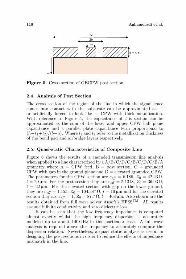
Figure 5. Cross section of GECPW post section.
2.4. Analysis of Post Section
The cross section of the region of the line in which the signal tracecomes into contact with the substrate can be approximated as —or artificially forced to look like — CPW with thick metallization.With reference to Figure 5, the capacitance of this section can beapproximated as the sum of the lower and upper CPW half planecapacitance and a parallel plate capacitance term proportional to(h+t1+t2)/(b−a). Where t1 and t2 refer to the metallization thicknessof the bond pad and airbridge layers respectively.
2.5. Quasi-static Characteristics of Composite Line
Figure 6 shows the results of a cascaded transmission line analysiswhen applied to a line characterized by a A/B/C/D/C/B/C/D/C/B/Ageometry where A = CPW feed, B = post section, C = groundedCPW with gap in the ground plane and D = elevated grounded CPW.The parameters for the CPW section are εeff = 6.186, Z0 = 42.23Ω,l = 20µm. For the post section they are εeff = 5.1318, Z0 = 36.93Ω,l = 22µm. For the elevated section with gap on the lower ground,they are εeff = 1.155, Z0 = 104.387Ω, l = 10µm and for the elevatedsection they are εeff = 1, Z0 = 87.7Ω, l = 468µm. Also shown are theresults obtained from full wave solver Ansoft’s HFSSTM. All resultsassume infinite conductivity and zero dielectric loss.
It can be seen that the low frequency impedance is computedalmost exactly whilst the high frequency dispersion is accuratelymodeled up to about 140 GHz in this particular case. A full waveanalysis is required above this frequency to accurately compute thedispersion relation. Nevertheless, a quasi static analysis is useful indesigning the post sections in order to reduce the effects of impedancemismatch in the line.

Progress In Electromagnetics Research B, Vol. 34, 2011 111
0 20 40 60 80 100 120 140 160
Frequency (GHz)
150
100
50
0
Z
(O
hm
)0
simulated
caculated
Figure 6. Comparison between simulated and calculated frequencydependent characteristic impedance for seven section line.
3. FABRICATION, MODELING AND MEASUREMENT
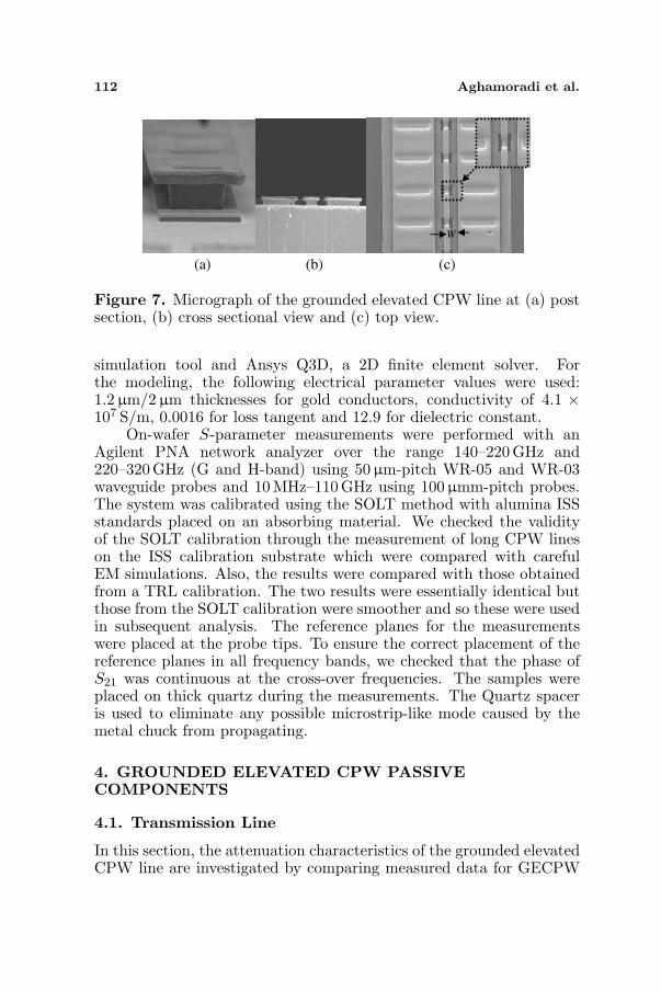
In order to realize the elevated structures, three fabrication steps wererequired. In the first step, the lower ground plane was defined bye-beam exposure and development of a 1.5µm thick layer of PMMAfollowed by electron beam evaporation and lift-off of a 50 nm/1.2µmthick nichrome/gold layer. The second and third steps employphotolithography and electroplating techniques to form the suspendedairbridge structures. The supporting posts for the elevated sectionswere formed by optical exposure and development of AZ4562 resist.The AZ4562 photoresist was spun with different speeds to achievethe desired thickness. The elevation height can be varied by definingthis resist thickness. In our process, spinning AZ4562 at the speedof 3000 rpm for 30 s leads to a thickness of roughly 6–6.5µm. Toachieve a greater thickness, this process can be repeated. Afterresist development, the metallization at this stage is achieved byevaporation of Ti/Au (50 nm/10 nm) followed by sputtering of 40 nmgold to provide the electrical contact for the subsequent electroplating.In order to define the elevated tracks, 2µm thick S1818 photoresistwas used followed by photolithography, development and ashing usinga dry etch machine. The sample was then metalized using goldelectroplating. Finally, different levels of exposure and developmentwere performed to remove all the resist. Figure 7 shows themicrographs of a typical grounded elevated CPW line.
The GECPW passive components on 625µm GaAs substrate weresimulated using Ansoft HFSSTM, a 3-D full wave electromagnetic
112 Aghamoradi et al.
W
(a) (b) (c)
Figure 7. Micrograph of the grounded elevated CPW line at (a) postsection, (b) cross sectional view and (c) top view.
simulation tool and Ansys Q3D, a 2D finite element solver. Forthe modeling, the following electrical parameter values were used:1.2µm/2µm thicknesses for gold conductors, conductivity of 4.1 ×10⁷ S/m, 0.0016 for loss tangent and 12.9 for dielectric constant.
On-wafer S-parameter measurements were performed with anAgilent PNA network analyzer over the range 140–220 GHz and220–320GHz (G and H-band) using 50µm-pitch WR-05 and WR-03waveguide probes and 10 MHz–110GHz using 100µmm-pitch probes.The system was calibrated using the SOLT method with alumina ISSstandards placed on an absorbing material. We checked the validityof the SOLT calibration through the measurement of long CPW lineson the ISS calibration substrate which were compared with carefulEM simulations. Also, the results were compared with those obtainedfrom a TRL calibration. The two results were essentially identical butthose from the SOLT calibration were smoother and so these were usedin subsequent analysis. The reference planes for the measurementswere placed at the probe tips. To ensure the correct placement of thereference planes in all frequency bands, we checked that the phase ofS21 was continuous at the cross-over frequencies. The samples wereplaced on thick quartz during the measurements. The Quartz spaceris used to eliminate any possible microstrip-like mode caused by themetal chuck from propagating.
4. GROUNDED ELEVATED CPW PASSIVECOMPONENTS
4.1. Transmission Line
In this section, the attenuation characteristics of the grounded elevatedCPW line are investigated by comparing measured data for GECPW

Progress In Electromagnetics Research B, Vol. 34, 2011 113
lines with that for conventional CPW lines. At low frequencies, thedominant loss mechanism of the CPW line is that due to the finiteconductivity of the metallization. At higher frequencies (dependent onthe particular lateral dimensions used and the substrate parameters)the losses are dominated by those due to radiation. However, theradiation losses are due mainly to the very presence of a highdielectric constant substrate. Across the whole range of frequenciesof interest, the substrate (tan δ) losses remain relatively low for aGaAs dielectric. Measured results indicate that, at low frequencies,where the substrate and radiation losses are relatively small and
0
1
2
3
4
5
6
0.01 100 200 300315
Frequency (GHz)
0.01 100 200 300325
Frequency (GHz)
0
-10
-20
-30
-40
-50
Insert
ion L
oss (
dB
/mm
)R
eflection C
oeffic
ient (d
B)
GECPW [MEAS]GECPW [SIM]
CPW [MEAS]
S GECPW [MEAS]11
S GECPW [SIM]11
S CPW [MEAS]11
(a)
(b)
Figure 8. Measured and simulated S-parameters for a GECPW andCPW. (a) Insertion loss per mm. (b) Reflection Coefficient (dB).

114 Aghamoradi et al.
attenuation is dominated by conductor loss, the attenuation of theCPW and GECPW lines are roughly comparable. However, athigh frequencies (above approximately 200 GHz for these particularCPW lateral dimensions), when the radiation and substrate losses ofCPW become significant, the GECPW line gains an advantage. TheGECPW line, unlike a conventional CPW line, is isolated from thesubstrate, has essentially zero dielectric loss and does not radiate toany significant extent. The post and feed sections, however, do havelosses of these types but because the majority of the physical extent ofthe line consists of elevated sections, the overall losses are reduced.
Figure 8 shows the measurement and simulation results for aline with a nominal impedance of 54 Ω and dimensions of signalwidth (W ) = 24µm, gap width (S) = 25µm and ground width(Wg) = 105µm. GECPW transmission line along with the resultsof conventional CPW for comparison. For this measurement, probingwas done on top of the elevated traces by placing two post sectionsclose together to make a stable landing pad.
It can be seen that, by using a grounded elevated CPW structure,improvements in the line performance in terms of loss/mm over aconventional CPW line can be achieved — especially at frequenciesabove 200GHz. The CPW attenuation results were compared withthose of [16, 17] and are in very close agreement, validating themeasurement process.
4.2. Transition to Coplanar waveguide
Elevated CPW lines cannot be suspended in air over their entire lengthbut must include post and feed sections — not only for mechanicalreasons but so they can be connected to transistors and/or passivecomponents. In Figure 9, measurements for a GECPW line withtransitions to CPW are compared with the results of a line with de-embedded transition.
Figure 9 clearly shows the deleterious effect of the transitionpad on the performance of GECPW line. Comparing the measuredinsertion loss for the GECPW line in Figure 8(a) with that of Figure 9it can be seen that the two methods of removing the effect of thetransition are in close agreement. Moreover, the effect shown inFigure 9 in the measured GECPW line without de-embedding andthe CPW line — that of a sudden increase in attenuation above210GHz — is shown to disappear using both techniques. The effectof the transition on the overall performance of grounded elevatedCPW becomes more significant at the frequencies for which CPWdegradation is more pronounced. The de-embedded grounded elevatedCPW line shows very low loss/mm at high mm-wave regimes — almost

Progress In Electromagnetics Research B, Vol. 34, 2011 115
0
1
2
3
4
5
6
0.01 100 200 300315
Frequency (GHz)
Insert
ion L
oss (
dB
/mm
) GECPW [De-embedded]GECPW [with transition taper]CPW
Figure 9. Measured S-parameters for a tapered GECPW, de-embedded GECPW and CPW transmission lines insertion loss/mm.
half the loss for the CPW line with the same characteristic impedance.Note that a rigorous optimization has not been conducted in the designof the CPW transitions and our design is based on a simple matchingof quasi-static characteristic impedances.
Some aspects of the discussed measurement results deserve furthercomment. The wavelength in the GECPW with air dielectric is longerthan in a CPW line with GaAs dielectric. Measured results for theCPW line reveal that the loss, in dB per wavelength, at 260 GHz,is about 1.3 dB/λg whilst for the GECPW line the figure is 1.6 dB/λg. The same measurement at 70 GHz shows 1.9 dB/λg for CPW linewhile 1.6 dB/λg is observed for GECPW. These results show that, interms of loss per wavelength and considering the effects of measurementerror, the two lines are broadly comparable over the d.c. — 320 GHzrange but also that, for a fixed length, the GECPW line exhibitsconsiderably less loss. The real advantage of the GECPW structureover conventional and previously reported elevated CPW structuresis that low loss transmission lines within a wide impedance range of5Ω–100Ω can easily be achieved by varying the elevation above thesubstrate. In contrast, CPW transmission line cannot satisfactorilyimplement such extremes of characteristic impedance due to excessivelosses [5]. Also, previously reported elevated structures tend only tosupport higher impedances with reasonable dimensions. The abilityto easily implement high and low impedances with GECPW lines ofreasonable dimensions can therefore be considered a great advantage.
Besides, in CPW and other previously reported elevated-CPW

116 Aghamoradi et al.
structures, small lateral dimensions (W + 2S) are required to achievelow radiation losses at mm-wave frequencies. In contrast, theradiation loss mechanism of the GECPW structure is, to a largeextent, independent of the lateral dimension. When the limitationsof the fabrication process are considered, it can be advantageous toavoid especially small gaps or signal widths such as are required toachieve low and high impedance lines in conventional CPW. Furtheradvantages are found in the design of passive circuit components suchas the matching stubs and filters described in following sections.
The results presented here suggest that grounded elevated CPWhas a performance comparable with conventional CPW at lowerfrequencies. Furthermore, the absence of high attenuation well into
W1
S2
S1
L 1 L 2
W2
Figure 10. Micrograph of open circuited stub. The stub dimensionsare L1 = 350, L2 = 145, S1 = 19.5, S2 = 26, W1 = 45, and W2 = 23.5.All dimensions are in microns.
10 110 210 300320
Frequency (GHz)
0
-10
-20
-30
-40
Ma
gn
itu
de
(d
B)
S , GE CPW [MEAS]21
S , GE CPW [MEAS]11
S , GE CPW [SIM]21
S , GE CPW [SIM]11
S , CPW [MEAS]11
S , CPW [MEAS]21
Figure 11. Measured and simulated S-parameters for a GE CPWopen-end shunt stub.

Progress In Electromagnetics Research B, Vol. 34, 2011 117
the sub-millimeter wave frequencies suggest reduced dielectric-relatedloss.
4.3. Open Circuit Matching Network
One of the coplanar waveguide components whose performance canbe improved is the open circuited matching network. To study theperformance of the open circuit stub using grounded elevated CPW, aseries of open circuited 90 shunt stubs were designed and fabricatedwith different center frequencies. A micrograph of an implementedGECPW matching network incorporating an open circuited stub isshown in Figure 10.
To demonstrate the stub characteristics, a comparison betweenthe measured and modeled characteristics of a matching network usingGECPW and the measured results of one implemented using CPW isgiven in Figure 11. The GECPW network shows an in-band-loss at the90 frequency (163GHz) of the stub of 0.9 dB and a 3 dB-bandwidthof 100 GHz. The CPW open stub shows an in-band-loss of 1.58 dB atthe frequency of 153GHz and a 3 dB-bandwidth of 112 GHz. This is areduction in loss of around 0.7 dB.
To achieve optimum performance for the GECPW network wedesigned the shunt connected line to have a higher impedance thanthe series lines. However, even a non-optimized GECPW networkmeasures superior performance with 1.2 dB insertion loss and abandwidth of 105 GHz. Increasing the elevation height from 6µm to13µm yielded an in-band-loss of 1 dB at 149 GHz with a bandwidthof 100GHz. This suggests that the performance of a GECPW opencircuit stub is fairly insensitive to elevation height. However, lowerelevation is advantageous in terms of yield and fabrication complexity.
S1
W1
L1
S2W
2
Figure 12. Micrograph of short circuited stub. The stub dimensionsare L1 = 251, S1 = 30, W1 = 24, S2 = 19.5 and W2 = 44.8. Alldimensions are in microns.

118 Aghamoradi et al.
Frequency (GHz)
0
-10
-20
-30
-40Ma
gn
itu
de
(d
B)
S , GE CPW [MEAS]21
S , GE CPW [MEAS]11
S , CPW [MEAS]21
S , CPW [MEAS]11
140 190 240 290 320
-50
-60
Figure 13. Measured S-parameters for GECPW short-end shunt stubwith 13µm elevation.
4.4. Short Circuit Matching Network
The short circuited shunt stub matching network, is a useful topologyfor a variety of circuits including band-pass filters, diode detectors andmatching/dc return networks. Figure 12 is a micrograph of such anetwork implemented using GECPW.
The performance of CPW short circuit matching stubs at highfrequencies has been investigated [4]. Figure 13 shows some measuredresults for CPW and GECPW short circuited matching stubs. Due tounwanted substrate effects at high frequencies, the CPW short circuitstub designed for 240 GHz exhibits a very large bandwidth and ripplesin the reflection coefficient. The loss at the center frequency is 1.8 dB.
Simulation results for CPW short circuit stub show a similar effectat these frequencies. The grounded elevated CPW short circuited stubwith a center frequency of 245 GHz and at 6µm elevation exhibits1.6 dB in-band loss at the center frequency with better matching to50Ω than the CPW short circuit stub but the performance is notgreatly enhanced. However, by increasing the elevation height to13µm, the performance of the short circuited GECPW matching stubis observed to improve drastically. Results for 13µm elevation alongwith those for a CPW stub resonating at a slightly lower frequency areshown in Figure 13.
In Figure 13, the GECPW stub shows 0.7 dB loss at the centerfrequency of 204 GHz compared with 1.8 dB for CPW at the centerfrequency of 185GHz.
Using a balanced shorted stub with 13µm elevation increases the

Progress In Electromagnetics Research B, Vol. 34, 2011 119
insertion loss at the center frequency to 1.35 dB and reduces the 3-dB bandwidth to 77GHz. The increased loss in this case is mainlyattributable to the increase in overall conductor loss.
In order to suppress the slotline mode at the discontinuities,additional supporting posts were used to connect the top and lowerground planes at the junctions. We tried stubs without these additionalconnecting posts and the response was very different from those shownin Figure 13. The bandwidth was much larger and the insertion losswas increased by at least 1.3 dB.
S2
W2
S1
W1
L1
L2
Figure 14. Micrograph of the 3rd order quarter-wavelength band-pass Filter. The filter dimensions are L1 = 270, L2 = 252, S1 = 37,S2 = 14, W1 = 21, and W2 = 44.5. All dimensions are in microns.
Frequency (GHz)
0
-15
-25
-35
-45Ma
gn
itu
de
(d
B)
S , GECPW [MEAS]21
S , GECPW [MEAS]11
S , CPW [MEAS]S , CPW [MEAS]11
140 190 240 290 325
-55
-65
-5
21
S , GECPW [SIM]21
S , GECPW [SIM]11
Figure 15. Measured and simulated S-parameters for a GE CPWband-pass filter.
120 Aghamoradi et al.
S1
L2
W1
L1
S2
W2
L3
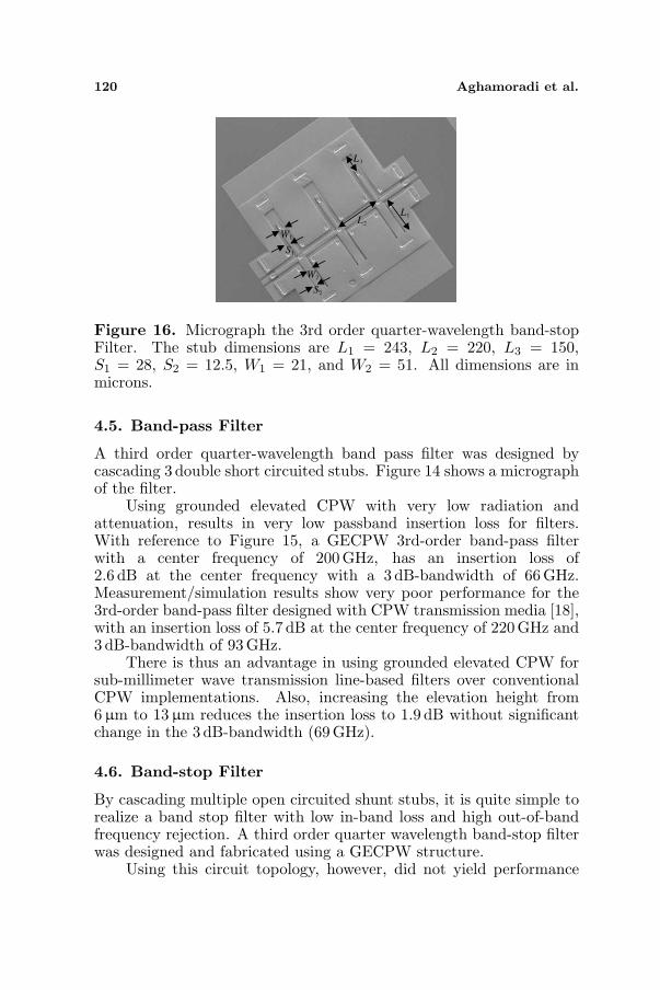
Figure 16. Micrograph the 3rd order quarter-wavelength band-stopFilter. The stub dimensions are L1 = 243, L2 = 220, L3 = 150,S1 = 28, S2 = 12.5, W1 = 21, and W2 = 51. All dimensions are inmicrons.
4.5. Band-pass Filter
A third order quarter-wavelength band pass filter was designed bycascading 3 double short circuited stubs. Figure 14 shows a micrographof the filter.
Using grounded elevated CPW with very low radiation andattenuation, results in very low passband insertion loss for filters.With reference to Figure 15, a GECPW 3rd-order band-pass filterwith a center frequency of 200 GHz, has an insertion loss of2.6 dB at the center frequency with a 3 dB-bandwidth of 66 GHz.Measurement/simulation results show very poor performance for the3rd-order band-pass filter designed with CPW transmission media [18],with an insertion loss of 5.7 dB at the center frequency of 220 GHz and3 dB-bandwidth of 93 GHz.
There is thus an advantage in using grounded elevated CPW forsub-millimeter wave transmission line-based filters over conventionalCPW implementations. Also, increasing the elevation height from6µm to 13µm reduces the insertion loss to 1.9 dB without significantchange in the 3 dB-bandwidth (69 GHz).
4.6. Band-stop Filter
By cascading multiple open circuited shunt stubs, it is quite simple torealize a band stop filter with low in-band loss and high out-of-bandfrequency rejection. A third order quarter wavelength band-stop filterwas designed and fabricated using a GECPW structure.
Using this circuit topology, however, did not yield performance

Progress In Electromagnetics Research B, Vol. 34, 2011 121
Frequency (GHz)
0
-20
-40
Magnitude (
dB
)
S , GECPW [MEAS]21
S , GECPW [MEAS]11
S , CPW [MEAS]
S , CPW [MEAS]11
140 190 240 290 325
-60
-80
21
S , GECPW [SIM]21
S , GECPW [SIM]11
Figure 17. Measured and simulated S-parameters for a GECPWband-stop filter.
greatly superior to CPW. Therefore, a combination of short and opencircuited shunt stubs was used to realize the band-stop filter, seeFigure 16. This improved the performance of the filter with higherout-of-band attenuation and lower in-band loss.
With reference to Figure 17, the 3rd-order quarter-wavelengthGECPW band stop filter shows 2.1 dB in-band loss at the centerfrequency of 230 GHz with a 3 dB bandwidth of 99 GHz. Comparedwith its CPW counterpart, the GECPW filter shows similar insertionloss but a 61 GHz reduction in the bandwidth. By increasing theelevation height from 6µm to 13µm, the in-band loss reduces to 1.5 dBwhile the 3 dB-bandwidth stays almost constant.
5. CONCLUSION
A new type of elevated CPW transmission line, Grounded elevatedCPW (GECPW), has been shown to provide low insertion loss and lowsensitivity to substrate effects at frequencies up to 320 GHz. Simpleequations have been formulated to facilitate design work and showgood agreement with simulation results and measurement. The MMICcompatible GECPW structure offers an extremely low insertion loss(2.5 dB/mm) at these frequencies which is almost 2.5 dB less thanthe insertion loss of an equivalent CPW line and 3.3 dB less than anelevated CPW line at the same frequency. Circuit components suchas short and open circuited stubs, band-pass filters and band-stop

122 Aghamoradi et al.
filters designed with the GECPW structure all show a performanceenhancement compared with CPW counterparts up to 320 GHz. Twomm-wave band pass filters — one implemented with CPW and theother with GECPW — show that a decrease of 3.1 dB in loss canbe achieved at the center frequency by using the new transmission linestructure. This is a considerable reduction in pass-band loss and amplydemonstrates the potential of the novel transmission line structure toenhance the performance of mm-wave circuits.
REFERENCES
1. Deal, W. R., X. B. Mei, V. Radisic, W. Yoshida, P. H. Liu,J. Uyeda, M. Barsky, T. Gaier, A. Fung, and R. Lai,“Demonstration of a S-MMIC LNA with 16-dB gain at 340 GHz,”IEEE Compound Semiconductor Integrated Circuit Symposium, 1–4, 2007.
2. Mei, X. B., W. Yoshida, P. H. Liu, J. Uyeda, J. Wang, W. Liu,D. Li, Y. M. Kim, M. Lange, T. P. Chin, T. Gaier, A. Fung,L. Samoska, and R. Lai, “35-nm InP HEMT SMMIC amplifierwith 4.4-dB gain at 308 GHz,” IEEE Electron. Device Letters,Vol. 28, No. 6, Jun. 2007.
3. Tessmann, A., A. Leuther, H. Massler, V. Hurm, M. Kuri,M. Zink, M. Riessle, and R. Losch, “High-gain submillimeter-wave mHEMT amplifier MMICs,” Microwave Symposium Digest(MTT), 1, 2010.
4. Aghamoradi, F., I. McGregor, and K. Elgaid, “Performanceenhancement of millimetre-wave resonators using elevated CPW,”Electron. Letters, Vol. 45, No. 25, 1326–1328, Dec. 2009.
5. Jackson, R. W., “Considerations in the use of coplanar waveguidefor millimetre-wave integrated circuits,” IEEE Trans. MicrowaveTheory Tech., Vol. 34, 1450–1456, Dec. 1986.
6. Weller, T. M., L. P. B. Katehi, and G. M. Rebeiz,“High performance microshield line components,” IEEE Trans.Microwave Theory Tech., Vol. 43, 534–543, Mar. 1995.
7. Schnieder, F., R. Doerner, and W. Heinrich, “High impedancecoplanar waveguides with low attenuation,” IEEE MicrowaveGuided Wave Lett., Vol. 6, 117–119, Mar. 1996.
8. Kim, H. T., S. Jung, J. H. Park, C. W. Baek, Y. K. Kim,and Y. Kwon, “A new micromachined overlap CPW structurewith low attenuation over wide impedance ranges,” IEEE Trans.Microwave Theory Tech., Vol. 49, No. 9, 2001.

Progress In Electromagnetics Research B, Vol. 34, 2011 123
9. McGregor, I., F. Aghamoradi, and K. Elgaid, “An approximateanalytical model for the quasi-static parameters of elevated CPWlines,” IEEE Trans. Microwave Theory Tech., Vol. 58, 3809,Dec. 2010.
10. Ghione, G. and C. U. Naldi, “Co planar waveguides for MMICapplications: Effect of upper shielding, conductor backing, finiteextent ground planes, and line-to-line coupling,” IEEE Trans.Microwave Theory Tech., 260–267, Vol. 35, 1987.
11. Hilberg, W., “From approximations to exact relations forcharacteristic impedances,” IEEE Trans. Microwave TheoryTech., Vol. 17, No. 5, 259–265, 1969.
12. Tang, W. C. and Y. L. Chow, “CAD formulas and theirinverses for microstrip, CPW and conductor-backed CPW, bysuccessive synthetic asymptotes,” Antennas and PropagationSociety International Symposium, Vol. 3, 394–397, 2001.
13. Chang, W. H., “Analytic IC-metal-line capacitance formulas,”IEEE Trans. Microwave Theory Tech., Vol. 24, 608–611, 1976;also Vol. 25, 712, 1977.
14. Ghione, G., M. Goana, G. L. Madonna, G. Omegna, M. Pirola,S. Bosso, D. Frassati, and A. Perasso, “Microwave modeling andcharacterization of thick coplanar waveguides on oxide-coatedlithium niobate substrates for electrooptical applications,” IEEETrans. Microwave Theory Tech., Vol. 47, No. 12, 2287–2293, 2002.
15. Ghione, G. and M. Goana, “Revisiting the partial-capacitanceapproach to the analysis of coplanar transmission lines onmultilayered substrates,” IEEE Trans. Microwave Theory Tech.,Vol. 51, No. 9, 2007–2014, 2003.
16. Cheng, H., J. F. Whitaker, T. M, and L. P. B. Katehi, “Terahetz-bandwidth characterzation of coplanar waveguide on dielectricmembrane via time domain electro-optic sampling,” IEEE MTT-S International Microwave Symposium Digest, Vol. 1, 477–480,1994.
17. Zehentner, J. and J. Machac, “Properties of CPW in the sub-mm wave range and its potential to radiate,” IEEE MTT-SInternational Microwave Symposium Digest, Vol. 2, 1061–1064,2000.
18. Aghamoradi, F., I. McGregor, and K. Elgaid, “H-bandelevated CPW band-pass filters on GaAs substrate,” MicrowaveConference (EuMC), 9–12, 2010.