low-cost assembly of uhf rfid chips and flexible...
TRANSCRIPT

Low-Cost Assembly of UHF RFID Chips and Flexible Substrate
Antennas by Magnetic Coupling Approach
F. Alimenti (1), M. Virili (1), P. Mezzanotte (1), V. Palazzari (1), M. M. Tentzeris (2), L. Roselli (1)
(1) University of Perugia, Perugia, ITALY (2) Georgia Institute of Technology, Atalanta, USA
Ahstract- This article deals with a novel low-cost technology for the assembly of flexible substrate antennas and UHF RFID Si chips. Such a technology exploits a magnetic coupling mechanism, thus avoiding the need for galvanic contacts between the Si chip and the antenna itself. The magnetic coupling is established by a planar transformer, whose primary and secondary windings are implemented on flexible substrate and Si chip respectively. As a result the Si chip can be assembled on the antenna with a mere placing and gluing process. First the idea has been validated by theory. Electromagnetic simulations of a square heterogeneous transformer (1.0 mm side) show a minimum loss of 0.6 dB at 900 MHz, under simultaneous matching conditions. Then a symmetrical PCB transformer (1.5 mm side) has been fabricated and tested. Measurements indicates a minimum loss of 0.3 dB at 900 MHz, thus confirming the validity of the proposed solution.
Index Terms- RFID, CMOS, heterogeneous integration, flexible electronics, ink-jet paper printed circuits, RF transformers.
I. INTRODUCTION
RFID tags working in the UHF frequency range relies on ultra-low power CMOS circuits and flexible substrate antennas [1]. Nowadays the typical cost of these tags is around $ 0.1, most of this amount being associated to the assembly of the CMOS die on the flexible substrate. Among several mounting processes, the most effective one [2] is based on Fluidic Self Assembly (FSA). With FSA, specifically shaped semiconductor devices are suspended in liquid and flowed over a surface which has correspondingly shaped holes or receptors on it and into which the devices settle. The shape of the devices and of the holes is designed so that the devices fall easily into place and are self-aligned. FSA is typically divided in six process steps, the last one being devoted to the electrical connection of the assembled CMOS chip via standard metalization techniques. Since the pads on the CMOS chips are relatively small in diameter (80 Mm or less) an accurate alignment is required.
In the present article the possibility of completely avoid the last FSA step (i.e. the electrical connection step) is considered. To this purpose the CMOS chip is magnetically coupled to the antenna realized on the flexible substrate, thus avoiding the need for galvanic contacts between the chip and the antenna itself. The magnetic coupling is established, as in Fig. 1, by a heterogeneous planar transformer, whose primary and secondary windings are implemented on flexible substrate and Si chip respectively. As a result the RFID chip can be mounted
978-1-4244-7732-6/101$26.00 ©201 0 IEEE 1532
on the flexible substrate by mere placing and gluing process steps. In particular the chip will be pad-less and completely passivated; the pad-ring being substituted by the secondary coil (S in Fig. 1) of the transformer.
Fig. 1. The RFID chip (C) is magnetically coupled to the antenna (A). Such a copupling is obtained by a transformer whose primary (P) and secondary (S) windings are fabricated on antenna substrate and Si chip respectively. In this way the need for galvanic connection between antenna and chip is avoided.
The first, and more obvious advantage of the novel design solution, is the possibility to further reduce mounting costs by cutting one step of FSA process. The second advantage is related to the market exploitation of flexible antennas on paper substrates [3]. These antennas can be fabricated by direct inkjet printing and, thus, are well suited for ultra-low cost RFID tags. The mounting of CMOS chips, however, has been never experimented, mainly because of the difficulty of establishing an electrical connection between the chip pads and the metal lines on paper substrate. This is specifically what the proposed solution will avoid.
II. HETEROGENEOUS TRANSFORMER SIMULATIONS
The proposed idea has first been validated by electromagnetic simulations. To this purpose a heterogeneous transformer between paper substrate and CMOS Si chip is considered. The geometry of such a transformer has been defined on the basis of the following constraints. On paper substrate the primary winding is assumed to be printed exploiting an inkjet technology as in [3]. The minimum metal track width and spacing is 50 Mm, corresponding to the maximum spatial
IMS 2010
resolution of the ink-jet printer. On silicon, a typical RFID chip size of 1 mm2 is considered. The secondary windings is substituted to the pad-ring of the chip and all the required tag electronics is assumed inside such a secondary coil.
The complete parameter set is quoted in Table I. Primary and secondary winding have been placed face-to-face as in Fig. 1 and spaced by a distance of 50/Lm. This spacing accounts for a glue layer with a relative permittivity equal to 2.75.
TABLE I
GEOMETRICAL PARAMETERS OF PAPER TO SI TRANSFORMER
Parameter Primary Secondary
material paper Si chip
number of turns 3 3
transformer side 1.0 mm 0.8 mm
track width 50 p,m 10 p,m
track spacing 50 p,m 5 p,m
track thickness 18 p,m 3 p,m
track a 58 MS/m 37 MS/m
substrate height 260 p,m 750 (Si bulk) p,m
16 (Si02) p,m
substrate c r 3.3 11.9 (Si bulk)
4.1 (Si02)
substrate tan <5 0.08
substrate a 0.2 mS/m
The electromagnetic simulation results (not reported here for sake of brevity) have then used to extract a transformer model, according to the scheme of Fig. 2. Such a model is valid in the frequency range from DC to 2 GHz. The transformer has a coupling factor k = 0.52 and a ratio n = 0.76. It is worth noting here that n does not correspond to the turn ratio (Nl = 3, N2 = 3, NdN2 = 1) because of the asymmetry between primary and secondary windings, the latter having a greater inductance.
C/2
R1 L 1 k L2 R2 . RFID C2 chip C1
A n : 1
C/2
Fig. 2. Transformer equivalent circuit adopted to study the chip to antenna (A) coupling. The extracted parameters for the simulated paper to Si transformer are: n = 0.76; k = 0.52; Lp = 4.8 nH; Rp = 00; L1 = 4.4 nH; R1 = 0.9 n; C1 = 70fF; L2 = 7.7 nH; R2 = 4.5 n; C2 = 50fF; C = 28fF.
The transformer model can finally be used to evaluate the coupling performance of the proposed design solution. The best power transfer between antenna and RFID chip is achieved in simultaneous matching conditions, i.e. when
978-1-4244-7732-6/10/$26.00 ©201 0 IEEE 1533
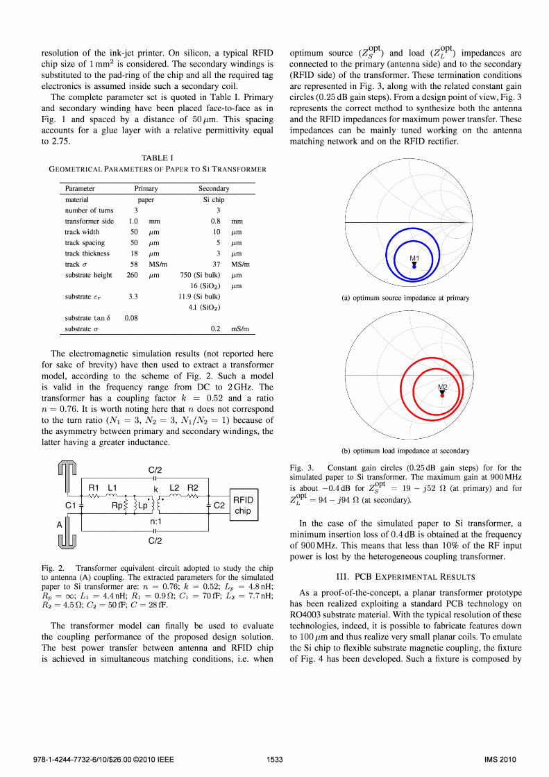
optimum source (Z�Pt) and load (Z�Pt
) impedances are connected to the primary (antenna side) and to the secondary (RFID side) of the transformer. These termination conditions are represented in Fig. 3, along with the related constant gain circles (0.25 dB gain steps). From a design point of view, Fig. 3 represents the correct method to synthesize both the antenna and the RFID impedances for maximum power transfer. These impedances can be mainly tuned working on the antenna matching network and on the RFID rectifier.
(a) optimum source impedance at primary
(b) optimum load impedance at secondary
Fig. 3. Constant gain circles (0.25 dB gain steps) for for the simulated paper to Si transformer. The maximum gain at 900 MHz
is about -0.4 dB for z�Pt = 19 - j52 n (at primary) and for
z�Pt = 94 - j94 n (at secondary).
In the case of the simulated paper to Si transformer, a minimum insertion loss of 0.4 dB is obtained at the frequency of 900 MHz. This means that less than 10% of the RF input power is lost by the heterogeneous coupling transformer.
III. PCB EXPERIMENTAL RESULTS
As a proof-of-the-concept, a planar transformer prototype has been realized exploiting a standard PCB technology on R04003 substrate material. With the typical resolution of these technologies, indeed, it is possible to fabricate features down to 100 /Lm and thus realize very small planar coils. To emulate the Si chip to flexible substrate magnetic coupling, the fixture of Fig. 4 has been developed. Such a fixture is composed by
IMS 2010

two separated PCBs each of them with a 3-turns winding. The outer terminal of the windings is fed by a 50 n microstrip line while, the inner one, is connected to the microstrip ground. Such a ground connection is provided by a via hole at the center of the winding and by a short metal track printed in the same layer of the microstrip ground, see Fig. 4(b). In this way is possible to remove the microstrip ground from the winding active area, thus resembling the ground-less structure of Fig. I.
(a)
(b)
Fig. 4. Mechanical drawing of the PCB test-fixture (a) and zoom of the transformer structure (b).
The geometrical parameters of the developed PCB transformer are quoted in Table II. Primary and secondary winding have been placed face-to-face as in Fig. 4(a). In this case the solder-resist film has been used to electrically isolate the two windings and, in this action, is similar to the Si02 passivation of the CMOS chip. The solder resist thickness is about 30 Mm whereas its relative permittivity is equal to 4. The two PCBs are equal thus giving a symmetrical transformer whose windings have a side of only 1.5 mm.
The fabricated test-fixture is shown in Fig. 5. In particular Fig. 5(a) illustrates one of the two PCBs with the small winding covered by solder resist and fed by the microstrip line. The complete transformer structure is depicted in Fig. 5(b) where a second PCB is added on top of the first one and kept in position by four plastic screws (i.e. no glue is used here).
978-1-4244-7732-6/10/$26.00 ©201 0 IEEE 1534
TABLE II
GEOMETRICAL PARAMETERS OF PCB TRANSFORMER
Parameter Primary Secondary
material R04003 R04003
number of turns 3 3
transformer side 1.5 mm 1.5 mm
track width 100 Mm 100 Mm
track spacing 100 Mm 100 Mm
track thickness 17 Mm 17 Mm
track a 58 MS/m 58 MS/m
substrate height 305 Mm 305 Mm
substrate c r 3.55 3.55
substrate tan c5 0.002 0.002
(a)
(b)
Fig. 5. Fabricated PCB test-fixture showing the primary winding alone (a) and the whole transformer (b). The latter has been obtained joining two equal planar windings in face-to-face configuration.
The structure of Fig. 5 has been experimentally characterized exploiting the vector network analyzer. The measured results are reported in Fig. 6 in a frequency range from DC to 2 GHz; i.e. including the RFID UHF 860 MHz and 960 MHz bands. The discontinuities associated to both the SMA connector and to the feeding microstrip lines have been removed from measured data by means of a de-embedding procedure. These data have been then compared to the electromagnetic simulations of the isolated transformer.
As it can be seen from Fig. 6 the overall agreement between measurements and simulations is good over the considered frequency range. At at 900 MHz the insertion loss is about 3.2 dB. This performance, however, is obtained in a 50 n measurement system. At the same frequency, the maximum
. . . I h· d· . zopt opt
gam m Slmu taneous matc mg con ItlOns (s = Z L
IMS 2010

0
CD -5 � .,.... C\J CJ) '0 -1 0 Q)
"0
.2 'c OJ (1l -1 5 E
-20 0
0
CD -2 � .,.... -4 CJ) '0 Q)
"0 -6 .2 'c OJ (1l
E -8
-1 0 0
H ••• �
� .
i / I
j simulations experiment .... + ....
0.5 1.5 frequency (GHz)
(a)
simulations experiment .... + ....
0.5 frequency (GHz)
(b)
1.5
2
2
Fig. 6. Comparison between measurements and simulations for the PCB transformer prototype. The feeding structure has been removed (de-embedding) from the measured response. These data are referred to a termination impedance of 50 n at both ports. The maximum gain
of this structure at 900 MHz is -0.3 dB for zopt = 58 - j67 n.
58 - j67 D) is, in fact, only -0.3 dB.
IV. CONCLUSIONS
This article shows that small RFID Si chip and large, flexible substrate, UHF antennas, can be efficiently coupled by means of a heterogeneous planar transformer. Primary and secondary windings of such a transformer are implemented on flexible substrate and Si chip respectively. As a result the Si chip will be completely pad-less, while a mere placing and gluing process will be required to assembly the whole RFID tag (i.e. antenna and Si chip together). The minimum insertion loss of 1 mm2 heterogeneous transformer is in the order of 0.6 dB at 900 MHz, as obtained from accurate electromagnetic simulations. Similar results have also been derived from the measurements of preliminary PCB prototypes.
978-1-4244-7732-6/10/$26.00 C201 0 IEEE 1535
Exploiting the proposed design solution, the costs associated to the assembly of RFID tags could be reduced and novel technologies, such as that of paper antennas produced by means of ink-jet printing, enabled at market level.
V. ACKNOWLEDGMENTS
Agilent Technologies and Computer Simulation Technologies are acknowledged for the donation of software licenses.
REFERENCES
[ 1] Alien Family of EPC Gen 2 RFJD Inlays, Alien Technology, 2008. [Online]. Available: http://www.alientechnology.com
[2] Alien Technology Corporation White Paper: Fluidic Self Assembly, Alien Technology, 1999. [Online]. Available: http://www.alientechnology.com
[3] L. Yang, A. Rida, R. Vyas, and M. M. Tentzeris, "RFID tag and RF structures on a paper substrate using inkjet-printing technology," IEEE Transaction on Microwave Theory and Techniques, vol. 55, no. 12, pp. 2894-2901, Dec. 2007.
IMS 2010