logicore ip block memory generator v7 - all programmable · the block memory generator can generate...
TRANSCRIPT

LogiCORE IP Block Memory Generator v7.3Product Guide
PG058 December 18, 2012

LogiCORE IP BMG v7.3 www.xilinx.com 2PG058 December 18, 2012
Table of Contents
SECTION I: SUMMARY
IP Facts
Chapter 1: OverviewFeature Summary. . . . . . . . . . . . . . . . . . . . . . . . . . . . . . . . . . . . . . . . . . . . . . . . . . . . . . . . . . . . . . . . . . 7Native Block Memory Generator Feature Summary . . . . . . . . . . . . . . . . . . . . . . . . . . . . . . . . . . . . . . 9AXI4 Interface Block Memory Generator Feature Summary . . . . . . . . . . . . . . . . . . . . . . . . . . . . . . 12Applications . . . . . . . . . . . . . . . . . . . . . . . . . . . . . . . . . . . . . . . . . . . . . . . . . . . . . . . . . . . . . . . . . . . . . 27Licensing and Ordering Information . . . . . . . . . . . . . . . . . . . . . . . . . . . . . . . . . . . . . . . . . . . . . . . . . . 27
Chapter 2: Product SpecificationPerformance. . . . . . . . . . . . . . . . . . . . . . . . . . . . . . . . . . . . . . . . . . . . . . . . . . . . . . . . . . . . . . . . . . . . . 29Resource Utilization. . . . . . . . . . . . . . . . . . . . . . . . . . . . . . . . . . . . . . . . . . . . . . . . . . . . . . . . . . . . . . . 29Port Descriptions . . . . . . . . . . . . . . . . . . . . . . . . . . . . . . . . . . . . . . . . . . . . . . . . . . . . . . . . . . . . . . . . . 38
Chapter 3: Designing with the CoreGeneral Design Guidelines . . . . . . . . . . . . . . . . . . . . . . . . . . . . . . . . . . . . . . . . . . . . . . . . . . . . . . . . . 46Clocking. . . . . . . . . . . . . . . . . . . . . . . . . . . . . . . . . . . . . . . . . . . . . . . . . . . . . . . . . . . . . . . . . . . . . . . . . 87Resets . . . . . . . . . . . . . . . . . . . . . . . . . . . . . . . . . . . . . . . . . . . . . . . . . . . . . . . . . . . . . . . . . . . . . . . . . . 87
SECTION II: VIVADO DESIGN SUITE
Chapter 4: Customizing and Generating the CoreGUI . . . . . . . . . . . . . . . . . . . . . . . . . . . . . . . . . . . . . . . . . . . . . . . . . . . . . . . . . . . . . . . . . . . . . . . . . . . . 89Generating the AXI4 Interface Block Memory Generator Core . . . . . . . . . . . . . . . . . . . . . . . . . . . 100Output Generation. . . . . . . . . . . . . . . . . . . . . . . . . . . . . . . . . . . . . . . . . . . . . . . . . . . . . . . . . . . . . . . 103
Chapter 5: Constraining the CoreRequired Constraints . . . . . . . . . . . . . . . . . . . . . . . . . . . . . . . . . . . . . . . . . . . . . . . . . . . . . . . . . . . . . 107Device, Package, and Speed Grade Selections. . . . . . . . . . . . . . . . . . . . . . . . . . . . . . . . . . . . . . . . . 107

LogiCORE IP BMG v7.3 www.xilinx.com 3PG058 December 18, 2012
Clock Frequencies . . . . . . . . . . . . . . . . . . . . . . . . . . . . . . . . . . . . . . . . . . . . . . . . . . . . . . . . . . . . . . . 107Clock Management . . . . . . . . . . . . . . . . . . . . . . . . . . . . . . . . . . . . . . . . . . . . . . . . . . . . . . . . . . . . . . 107Clock Placement. . . . . . . . . . . . . . . . . . . . . . . . . . . . . . . . . . . . . . . . . . . . . . . . . . . . . . . . . . . . . . . . . 107Banking . . . . . . . . . . . . . . . . . . . . . . . . . . . . . . . . . . . . . . . . . . . . . . . . . . . . . . . . . . . . . . . . . . . . . . . . 108Transceiver Placement . . . . . . . . . . . . . . . . . . . . . . . . . . . . . . . . . . . . . . . . . . . . . . . . . . . . . . . . . . . 108I/O Standard and Placement. . . . . . . . . . . . . . . . . . . . . . . . . . . . . . . . . . . . . . . . . . . . . . . . . . . . . . . 108
Chapter 6: Detailed Example DesignDirectory and File Contents. . . . . . . . . . . . . . . . . . . . . . . . . . . . . . . . . . . . . . . . . . . . . . . . . . . . . . . . 109Example Design . . . . . . . . . . . . . . . . . . . . . . . . . . . . . . . . . . . . . . . . . . . . . . . . . . . . . . . . . . . . . . . . . 109
SECTION III: ISE DESIGN SUITE
Chapter 7: Customizing and Generating the CoreGUI . . . . . . . . . . . . . . . . . . . . . . . . . . . . . . . . . . . . . . . . . . . . . . . . . . . . . . . . . . . . . . . . . . . . . . . . . . . 111Parameter Values in the XCO File . . . . . . . . . . . . . . . . . . . . . . . . . . . . . . . . . . . . . . . . . . . . . . . . . . . 127Output Generation. . . . . . . . . . . . . . . . . . . . . . . . . . . . . . . . . . . . . . . . . . . . . . . . . . . . . . . . . . . . . . . 129
Chapter 8: Constraining the CoreRequired Constraints . . . . . . . . . . . . . . . . . . . . . . . . . . . . . . . . . . . . . . . . . . . . . . . . . . . . . . . . . . . . . 135Device, Package, and Speed Grade Selections. . . . . . . . . . . . . . . . . . . . . . . . . . . . . . . . . . . . . . . . . 135Clock Frequencies . . . . . . . . . . . . . . . . . . . . . . . . . . . . . . . . . . . . . . . . . . . . . . . . . . . . . . . . . . . . . . . 135Clock Management . . . . . . . . . . . . . . . . . . . . . . . . . . . . . . . . . . . . . . . . . . . . . . . . . . . . . . . . . . . . . . 135Clock Placement. . . . . . . . . . . . . . . . . . . . . . . . . . . . . . . . . . . . . . . . . . . . . . . . . . . . . . . . . . . . . . . . . 135Banking . . . . . . . . . . . . . . . . . . . . . . . . . . . . . . . . . . . . . . . . . . . . . . . . . . . . . . . . . . . . . . . . . . . . . . . . 135Transceiver Placement . . . . . . . . . . . . . . . . . . . . . . . . . . . . . . . . . . . . . . . . . . . . . . . . . . . . . . . . . . . 136I/O Standard and Placement. . . . . . . . . . . . . . . . . . . . . . . . . . . . . . . . . . . . . . . . . . . . . . . . . . . . . . . 136
Chapter 9: Detailed Example DesignDirectory and File Contents. . . . . . . . . . . . . . . . . . . . . . . . . . . . . . . . . . . . . . . . . . . . . . . . . . . . . . . . 137Example Design . . . . . . . . . . . . . . . . . . . . . . . . . . . . . . . . . . . . . . . . . . . . . . . . . . . . . . . . . . . . . . . . . 137Demonstration Test Bench . . . . . . . . . . . . . . . . . . . . . . . . . . . . . . . . . . . . . . . . . . . . . . . . . . . . . . . . 137Implementation . . . . . . . . . . . . . . . . . . . . . . . . . . . . . . . . . . . . . . . . . . . . . . . . . . . . . . . . . . . . . . . . . 139Simulation . . . . . . . . . . . . . . . . . . . . . . . . . . . . . . . . . . . . . . . . . . . . . . . . . . . . . . . . . . . . . . . . . . . . . 140Messages and Warnings . . . . . . . . . . . . . . . . . . . . . . . . . . . . . . . . . . . . . . . . . . . . . . . . . . . . . . . . . . 141
SECTION IV: APPENDICES

LogiCORE IP BMG v7.3 www.xilinx.com 4PG058 December 18, 2012
Appendix A: Verification, Compliance, and InteroperabilitySimulation . . . . . . . . . . . . . . . . . . . . . . . . . . . . . . . . . . . . . . . . . . . . . . . . . . . . . . . . . . . . . . . . . . . . . 143
Appendix B: MigratingMigration Overview. . . . . . . . . . . . . . . . . . . . . . . . . . . . . . . . . . . . . . . . . . . . . . . . . . . . . . . . . . . . . . 144Differences Between Cores . . . . . . . . . . . . . . . . . . . . . . . . . . . . . . . . . . . . . . . . . . . . . . . . . . . . . . . . 145Using the Migration Kit . . . . . . . . . . . . . . . . . . . . . . . . . . . . . . . . . . . . . . . . . . . . . . . . . . . . . . . . . . . 149Migrating a Design Manually . . . . . . . . . . . . . . . . . . . . . . . . . . . . . . . . . . . . . . . . . . . . . . . . . . . . . . 155
Appendix C: DebuggingFinding Help on Xilinx.com . . . . . . . . . . . . . . . . . . . . . . . . . . . . . . . . . . . . . . . . . . . . . . . . . . . . . . . . 168Debug Tools . . . . . . . . . . . . . . . . . . . . . . . . . . . . . . . . . . . . . . . . . . . . . . . . . . . . . . . . . . . . . . . . . . . . 169Simulation Debug. . . . . . . . . . . . . . . . . . . . . . . . . . . . . . . . . . . . . . . . . . . . . . . . . . . . . . . . . . . . . . . . 171Hardware Debug . . . . . . . . . . . . . . . . . . . . . . . . . . . . . . . . . . . . . . . . . . . . . . . . . . . . . . . . . . . . . . . . 171Interface Debug . . . . . . . . . . . . . . . . . . . . . . . . . . . . . . . . . . . . . . . . . . . . . . . . . . . . . . . . . . . . . . . . . 172
Appendix D: Native Block Memory Generator Supplemental Information
Appendix E: Additional ResourcesXilinx Resources . . . . . . . . . . . . . . . . . . . . . . . . . . . . . . . . . . . . . . . . . . . . . . . . . . . . . . . . . . . . . . . . . 208References . . . . . . . . . . . . . . . . . . . . . . . . . . . . . . . . . . . . . . . . . . . . . . . . . . . . . . . . . . . . . . . . . . . . . 208Technical Support . . . . . . . . . . . . . . . . . . . . . . . . . . . . . . . . . . . . . . . . . . . . . . . . . . . . . . . . . . . . . . . 208Revision History . . . . . . . . . . . . . . . . . . . . . . . . . . . . . . . . . . . . . . . . . . . . . . . . . . . . . . . . . . . . . . . . . 209Notice of Disclaimer. . . . . . . . . . . . . . . . . . . . . . . . . . . . . . . . . . . . . . . . . . . . . . . . . . . . . . . . . . . . . . 209

LogiCORE IP BMG v7.3 www.xilinx.com 5PG058 December 18, 2012
SECTION I: SUMMARY
IP Facts
Overview
Product Specification
Designing with the Core
LogiCORE IP BMG v7.3 www.xilinx.com 6PG058 December 18, 2012 Product Specification
IntroductionThe Xilinx LogiCORE ™ IP Block Memory Generator (BMG) core is an advanced memory constructor that generates area and performance-optimized memories using embedded block RAM resources in Xilinx FPGAs. Users can quickly create optimized memories to leverage the performance and features of block RAMs in Xilinx FPGAs.
The BMG core supports both Native and AXI4 interfaces.
The Native interface BMG core configurations support the same standard BMG functions delivered by previous versions of the Block Memory Generator (up to and including version 4.3). Port interface names are identical.
The AXI4 interface configuration of the BMG core is derived from the Native interface BMG configuration and adds an industry-standard bus protocol interface to the core. Two AXI4 interface styles are available: AXI4 and AXI4-Lite.
FeaturesFor details on the features of each interface, see Feature Summary in Chapter 1.
IP Facts
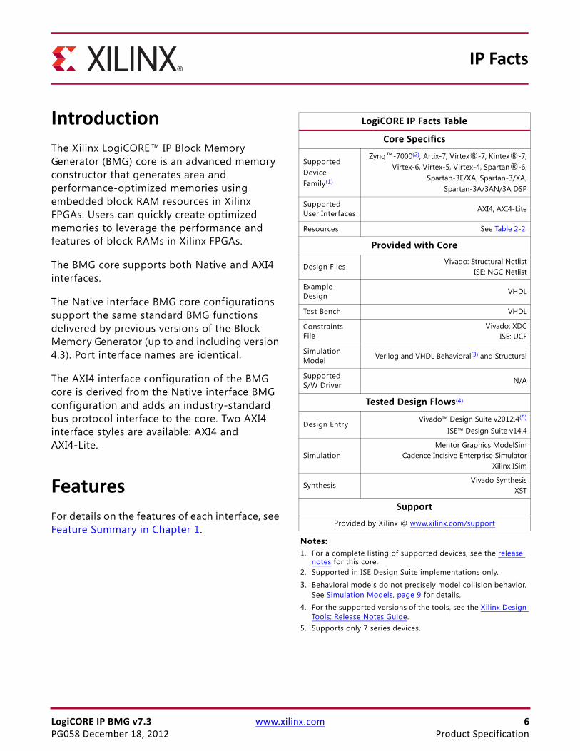
LogiCORE IP Facts Table
Core Specifics
Supported Device Family(1)
Zynq™-7000(2), Artix-7, Virtex®-7, Kintex®-7,Virtex-6, Virtex-5, Virtex-4, Spartan®-6,
Spartan-3E/XA, Spartan-3/XA,Spartan-3A/3AN/3A DSP
Supported User Interfaces AXI4, AXI4-Lite
Resources See Table 2-2.
Provided with Core
Design FilesVivado: Structural Netlist
ISE: NGC Netlist
Example Design VHDL
Test Bench VHDL
Constraints File
Vivado: XDCISE: UCF
Simulation Model Verilog and VHDL Behavioral(3) and Structural
Supported S/W Driver N/A
Tested Design Flows(4)
Design EntryVivado™ Design Suite v2012.4(5)
ISE™ Design Suite v14.4
Simulation Mentor Graphics ModelSim
Cadence Incisive Enterprise SimulatorXilinx ISim
SynthesisVivado Synthesis
XST
SupportProvided by Xilinx @ www.xilinx.com/support
Notes: 1. For a complete listing of supported devices, see the release
notes for this core.2. Supported in ISE Design Suite implementations only.
3. Behavioral models do not precisely model collision behavior. See Simulation Models, page 9 for details.
4. For the supported versions of the tools, see the Xilinx Design Tools: Release Notes Guide.
5. Supports only 7 series devices.

LogiCORE IP BMG v7.3 www.xilinx.com 7PG058 December 18, 2012
Chapter 1
OverviewThe Block Memory Generator core uses embedded Block Memory primitives in Xilinx FPGAs to extend the functionality and capability of a single primitive to memories of arbitrary widths and depths. Sophisticated algorithms within the Block Memory Generator core produce optimized solutions to provide convenient access to memories for a wide range of configurations.
The Block Memory Generator has two fully independent ports that access a shared memory space. Both A and B ports have a Write and a Read interface. In Zynq-7000, 7 series, Virtex-6, Virtex-5 and Virtex-4 FPGA architectures, each of the four interfaces can be uniquely configured with a different data width. When not using all four interfaces, the user can select a simplif ied memory configuration (for example, a Single-Port Memory or Simple Dual-Port Memory) to reduce FPGA resource utilization.
The Block Memory Generator is not completely backward-compatible with the discontinued legacy Single-Port Block Memory and Dual-Port Block Memory cores; for information about the differences, see Appendix B, Migrating.
Feature Summary
Features Common to the Native Interface and AXI4 BMG Cores• Optimized algorithms for minimum block RAM resource utilization or low power
utilization
• Configurable memory initialization
• Individual Write enable per byte in Zynq ™-7000, Kintex ™-7, Virtex ®-7, Virtex-6, Virtex-5, Virtex-4, Spartan ®-6, and Spartan-3A/XA DSP with or without parity
• Optimized VHDL and Verilog behavioral models for fast simulation times; structural simulation models for precise simulation of memory behaviors
• Selectable operating mode per port: WRITE_FIRST, READ_FIRST, or NO_CHANGE
• Smaller f ixed primitive configurations are now possible in Spartan-6 devices with the introduction of the new Spartan-6 device 9K primitives
• Lower data widths for Zynq-7000, 7 series, and Virtex-6 devices in SDP mode

LogiCORE IP BMG v7.3 www.xilinx.com 8PG058 December 18, 2012
Feature Summary
• VHDL example design and demonstration test bench demonstrating the IP core design flow, including how to instantiate and simulate it
Native Block Memory Generator Specific Features• Generates Single-port RAM, Simple Dual-port RAM, True Dual-port RAM, Single-port
ROM, and Dual-port ROM
• Supports data widths from 1 to 4608 bits and memory depths from 2 to 9M words (limited only by memory resources on selected part)
• Configurable port aspect ratios for dual-port configurations and Read-to-Write aspect ratios in Virtex-6, Virtex-5, and Virtex-4 FPGAs
• Supports the built-in Hamming Error Correction Capability (ECC) available in Zynq-7000, 7 series, Virtex-6 and Virtex-5 devices for data widths greater than 64 bits. Error injection pins in Zynq-7000, 7 series, and Virtex-6 allow insertion of single and double-bit errors
• Supports soft Hamming Error Correction (Soft ECC) in Zynq-7000, 7 series, Virtex-6, and Spartan-6 devices for data widths less than 64 bits.
• Option to pipeline DOUT bus for improved performance in specif ic configurations
• Choice of reset priority for output registers between priority of SR (Set Reset) or CE (Clock Enable) in Zynq-7000, 7 series, Virtex-6, and Spartan-6 families
• Asynchronous reset in Spartan-6 devices
• Performance up to 450 MHz
AXI4 Interface Block Memory Generator Specific Features• Supports AXI4 and AXI4-Lite interface protocols
• AXI4 compliant Memory and Peripheral Slave types
• Independent Read and Write Channels
• Zero delay datapath
• Supports registered outputs for handshake signals
• INCR burst sizes up to 256 data transfers
• WRAP bursts of 2, 4, 8, and 16 data beats
• AXI narrow and unaligned burst transfers
• Simple Dual-port RAM primitive configurations
• Performance up to 300 MHz
• Supports data widths from up to 256 bits and memory depths from 2 to 9 M words (limited only by memory resources on selected part)

LogiCORE IP BMG v7.3 www.xilinx.com 9PG058 December 18, 2012
Native Block Memory Generator Feature Summary
• Symmetric aspect ratios
• Asynchronous active low reset
Simulation ModelsThe Block Memory Generator core provides two types of functional simulation models:
• Behavioral Simulation Models (VHDL and Verilog)
• Structural/UniSim based Simulation Models (VHDL and Verilog)
The behavioral simulation models provide a simplif ied model of the core while the structural simulation models (UniSim) are an accurate modeling of the internal structure of the core. The behavioral simulation models are written purely in RTL and simulate faster than the structural simulation models and are ideal for functional debugging. Moreover, the memory is modeled in a two-dimensional array, making it easier to probe contents of the memory.
The structural simulation model uses primitive instantiations to model the behavior of the core more precisely. Use the structural simulation model to accurately model memory collision behavior and 'x' output generation. Note that simulation time is longer and debugging may be more diff icult. The Simulation Files options in the CORE Generator Project Options determine the type of functional simulation models generated. Table 1-1 defines the differences between the two functional simulation models.
Native Block Memory Generator Feature Summary
Supported DevicesTable 1-2 shows the families and sub-families supported by the Block Memory Generator.
Table 1-1: Differences between Simulation Models
Behavioral Models Structural Models (Unisim)
When core output is undefined Never generates ‘X’ Generates ‘X’ to match core
Out-of-range address access Optionally flags a warning message Generates ‘X’
Collision behavior Does not generate ‘X’ on output, and flags a warning message Generates ‘X’ to match core
Byte-Write collision behavior Flags all byte-Write collisions Does not flag collisions if byte-writes do not overlap

LogiCORE IP BMG v7.3 www.xilinx.com 10PG058 December 18, 2012
Native Block Memory Generator Feature Summary
Memory TypesThe Block Memory Generator core uses embedded block RAM to generate five types of memories:
• Single-port RAM
• Simple Dual-port RAM
• True Dual-port RAM
• Single-port ROM
• Dual-port ROM
For dual-port memories, each port operates independently. Operating mode, clock frequency, optional output registers, and optional pins are selectable per port. For Simple Dual-port RAM, the operating modes are not selectable. See Collision Behavior, page 59 for additional information.
Selectable Memory Algorithm
The core configures block RAM primitives and connects them together using one of the following algorithms:
• Minimum Area Algorithm: The memory is generated using the minimum number of block RAM primitives. Both data and parity bits are utilized.
Table 1-2: Supported FPGA Families and Sub-Families
FPGA Family Sub-Family
Spartan-3
Spartan-3E
Spartan-3A
Spartan-3AN
Spartan-3A DSP
Spartan-6 LX/LXT
Virtex-4 LX/FX/SX
Virtex-5 LXT/FXT/SXT/TXT
Virtex-6 CXT/HXT/LXT/SXT
Virtex-7 XT
Kintex-7
Artix ™-7
Zynq-7000

LogiCORE IP BMG v7.3 www.xilinx.com 11PG058 December 18, 2012
Native Block Memory Generator Feature Summary
• Low Power Algorithm: The memory is generated such that the minimum number of block RAM primitives are enabled during a Read or Write operation.
• Fixed Primitive Algorithm: The memory is generated using only one type of block RAM primitive. For a complete list of primitives available for each device family, see the data sheet for that family.
Configurable Width and Depth
The Block Memory Generator can generate memory structures from 1 to 4096 bits wide, and at least two locations deep. The maximum depth of the memory is limited only by the number of block RAM primitives in the target device.
Selectable Operating Mode per Port
The Block Memory Generator supports the following block RAM primitive operating modes: WRITE FIRST, READ FIRST, and NO CHANGE. Each port may be assigned its own operating mode.
Selectable Port Aspect Ratios
The core supports the same port aspect ratios as the block RAM primitives:
• In all supported device families, the A port width may differ from the B port width by a factor of 1, 2, 4, 8, 16, or 32.
• In Zynq-7000, 7 series, Virtex-6, Virtex-5 and Virtex-4 FPGA-based memories, the Read width may differ from the Write width by a factor of 1, 2, 4, 8, 16, or 32 for each port. The maximum ratio between any two of the data widths (DINA, DOUTA, DINB, and DOUTB) is 32:1.
Optional Byte-Write Enable
In Zynq-7000, 7 series, Virtex-6, Virtex-5, Virtex-4, Spartan-6, and Spartan-3A/3A DSP FPGA-based memories, the Block Memory Generator core provides byte-Write support for memory widths which are multiples of eight (no parity) or nine bits (with parity).
Optional Output Registers
The Block Memory Generator provides two optional stages of output registering to increase memory performance. The output registers can be chosen for port A and port B separately. The core supports the Zynq-7000, 7 series, Virtex-6, Virtex-5, Virtex-4, Spartan-6, and Spartan-3A DSP embedded block RAM registers as well as registers implemented in the FPGA fabric. See Output Register Configurations, page 187 for more information about using these registers.

LogiCORE IP BMG v7.3 www.xilinx.com 12PG058 December 18, 2012
AXI4 Interface Block Memory Generator Feature Summary
Optional Pipeline Stages
The core provides optional pipeline stages within the MUX, available only when the registers at the output of the memory core are enabled and only for specific configurations. For the available configurations, the number of pipeline stages can be 1, 2, or 3. For detailed information, see Optional Pipeline Stages, page 64.
Optional Enable Pin
The core provides optional port enable pins (ENA and ENB) to control the operation of the memory. When deasserted, no Read, Write, or reset operations are performed on the respective port. If the enable pins are not used, it is assumed that the port is always enabled.
Optional Set/Reset Pin
The core provides optional set/reset pins (RSTA and RSTB) for each port that initialize the Read output to a programmable value.
Memory Initialization
The memory contents can be optionally initialized using a memory coeff icient (COE) f ile or by using the default data option. A COE f ile can define the initial contents of each individual memory location, while the default data option defines the initial content of all locations.
Hamming Error Correction Capability
Simple Dual-port RAM memories support the built-in FPGA Hamming Error Correction Capability (ECC) available in the Zynq-7000, 7 series, Virtex-6 and Virtex-5 FPGA block RAM primitives for data widths greater than 64 bits. The BuiltIn_ECC (ECC) memory automatically detects single- and double-bit errors, and is able to auto-correct the single-bit errors.
For data widths of 64 bits or less, a soft Hamming Error Correction implementation is available for Zynq-7000, 7 series, Virtex-6, and Spartan-6 designs.
AXI4 Interface Block Memory Generator Feature Summary
OverviewAXI4 Interface Block Memories are built on the Native Interface Block Memories (see Figure 1-1). Two AXI4 interface styles are available - AXI4 and AXI4-Lite. The core can also be further classif ied as a Memory Slave or as a Peripheral Slave. In addition to applications

LogiCORE IP BMG v7.3 www.xilinx.com 13PG058 December 18, 2012
AXI4 Interface Block Memory Generator Feature Summary
supported by the Native Interface Block Memories, AXI4 Block Memories can also be used in AXI4 System Bus applications and Point-to-Point applications.
All communication in the AXI protocol is performed using f ive independent channels. Each of the f ive independent channels consists of a set of information signals and uses a two-way VALID and READY handshake mechanism. The information source uses the VALID signal to show when valid data or control information is available on the channel. The information destination uses the READY signal to show when it can accept the data.
In Figure 1-2, the information source generates the VALID signal to indicate when data is available.
The destination generates the READY signal to indicate that it can accept the data, and transfer occurs only when both the VALID and READY signals are high.
The AXI4 Block Memory Generator is an AXI4 endpoint Slave IP and can communicate with multiple AXI4 Masters in an AXI4 System or with Standalone AXI4 Masters in point to point applications. The core supports Simple Dual Port RAM configurations. Because AXI4 Block Memories are built using Native interface Block Memories, they share many common features.
X-Ref Target - Figure 1-1
Figure 1-1: AXI4 Interface BMG Block Diagram
X-Ref Target - Figure 1-2
Figure 1-2: AXI4 Interface Handshake Timing Diagram

LogiCORE IP BMG v7.3 www.xilinx.com 14PG058 December 18, 2012
AXI4 Interface Block Memory Generator Feature Summary
All Write operations are initiated on the Write Address Channel (AW) of the AXI bus. The AW channel specif ies the type of Write transaction and the corresponding address information. The Write Data Channel (W) communicates all Write data for single or burst Write operations. The Write Response Channel (B) is used as the handshaking or response to the Write operation.
On Read operations, the Read Address Channel (AR) communicates all address and control information when the AXI master requests a Read transfer. When the Read data is available to send back to the AXI master, the Read Data Channel (R) transfers the data and status of the Read operation
Applications
AXI4 Block Memories - Memory Slave Mode
AXI4 Block Memories in Memory Slave mode are optimized for Memory Mapped System Bus implementations. The AXI4 Memory Slave Interface Type supports aligned, unaligned or narrow transfers for incremental or wrap bursts.
Figure 1-3 shows an example application for the AXI4 Memory Slave Interface Type with an AXI4 Interconnect for Multi Master AXI4 applications. Minimum memory requirement for this configuration is set to 4K bytes. Data widths supported by this configuration include 32, 64, 128 or 256 bits
AXI4-Lite Block Memories - Memory Slave Mode
AXI4-Lite Block Memories in Memory Slave mode are optimized for the AXI4-Lite interface. They can be used in implementations requiring simple Control/Status Accesses. AXI4-Lite Memory Slave Interface Type supports only single burst transactions.
X-Ref Target - Figure 1-3
Figure 1-3: AXI4 Memory Slave Application Diagram

LogiCORE IP BMG v7.3 www.xilinx.com 15PG058 December 18, 2012
AXI4 Interface Block Memory Generator Feature Summary
Figure 1-4 shows an example application for AXI4-Lite Memory Slave Interface Type with an AXI4-Lite Interconnect to manage Control/Status Accesses. The minimum memory requirement for this configuration is set to 4K bytes. Data widths of 32 and 64 bits are supported by this configuration.
AXI4 Block Memories - Peripheral Slave Mode
AXI4 Block Memories in Peripheral Slave mode are optimized for a system or applications requiring data transfers that are grouped together in packets. The AXI4 Peripheral Slave supports aligned /unaligned addressing for incremental bursts.
Figure 1-5 shows an example application for the AXI4 Peripheral Slave Interface Type in a Point-to-point buffered link list application. There is no minimum memory requirement set for this configuration. Data widths supported by this configuration include 8, 16, 32, 64, 128 and 256 bits.
X-Ref Target - Figure 1-4
Figure 1-4: AXI4-Lite Memory Slave Application Diagram
X-Ref Target - Figure 1-5
Figure 1-5: AXI4 Peripheral Slave Application Diagram

LogiCORE IP BMG v7.3 www.xilinx.com 16PG058 December 18, 2012
AXI4 Interface Block Memory Generator Feature Summary
AXI4-Lite Block Memories - Peripheral Slave Mode
AXI4-Lite Block Memories in Peripheral Slave mode are optimized for the AXI4-Lite interface. They can be used in implementations requiring single burst transactions.
Figure 1-8 shows an example application for the AXI4-Lite Memory Slave Interface Type in a Point-to-point application. There is no minimum memory requirement set for this configuration. Data widths supported by this configuration include 8, 16, 32 and 64 bits.
Supported Devices
AXI4 BMG Core Channel Handshake SequenceFigure 1-9 and Figure 1-10 illustrates an example handshake sequence for AXI4 BMG core. Figure 1-9 illustrates single burst Write operations to block RAM. By default the AWREADY signal is asserted on the bus so that the address can be captured immediately during the clock cycle when both AWVALID and AWREADY are asserted. (With the default set in this manner, there is no need to wait an extra clock cycle AWREADY to be asserted first.) By default, the WREADY signal will be de-asserted. Upon detecting AWVALID being asserted, the WREADY signal will be asserted (AXI4 BMG core has registered an AXI Address and is ready to accept Data), and when WVALID is also asserted, writes will be performed to the block RAM. If the write data channel (WVALID) is presented prior to the write address
X-Ref Target - Figure 1-6X-Ref Target - Figure 1-74.2.4AXI4-Lite Block Memories - Peripheral Slave ModeX-Ref Target - Figure 1-8
Figure 1-8: AXI4-Lite Peripheral Slave Application Diagram
Table 1-3: AXI4 BMG Supported FPGA Families and Sub-Families
FPGA Family Sub-Family
Spartan-6 LX/LXT
Virtex-6 CXT/HXT/LXT/SXT
Virtex-7 XT
Kintex-7
Artix-7
Zynq-7000

LogiCORE IP BMG v7.3 www.xilinx.com 17PG058 December 18, 2012
AXI4 Interface Block Memory Generator Feature Summary
channel valid (AWVALID) assertion, the write transactions will not be initiated until the write address channel has valid information.
The AXI4 Block Memory core will assert BVALID for each transaction only after the last data transfer is accepted. The core also will not wait for the master to assert BREADY before asserting BVALID.
Figure 1-9 illustrates single burst Read operations to block RAM. The registered ARREADY signal output on the AXI Read Address Channel interface defaults to a high assertion. The AXI Read FSM can accept the read address in the clock cycle where the ARVALID signal is f irst valid.
The AXI Read FSM can accept a same clock cycle assertion of the RREADY by the master if the master can accept data immediately. When the RREADY signal is asserted on the AXI bus by the master, the Read FSM will either negate the RVALID signal or will place next valid data on the AXI Bus.
X-Ref Target - Figure 1-9
Figure 1-9: AXI4-Lite Single Burst Write Transactions

LogiCORE IP BMG v7.3 www.xilinx.com 18PG058 December 18, 2012
AXI4 Interface Block Memory Generator Feature Summary
For more details on AXI4 Channel handshake sequences refer to the “Channel Handshake” section of the AXI protocol specification [Ref 1].
AXI4 Lite Single Burst TransactionsFor AXI4 Lite interfaces, all transactions are burst length of one and all data accesses are the same size as the width of the data bus. Figure 1-9 and Figure 1-10 illustrates timing of AXI 32-bit write operations to the 32-bit wide BRAM. Figure 1-9 example illustrates single burst Write operations to block RAM addresses 0x1000h and 0x1004h. Figure 1-10 illustrates single burst Read operations to block RAM addresses 0x1000h and 0x1004h.
AXI4 Incremental Burst SupportFigure 1-11 illustrates an example of the timing for an AXI Write burst of four words to a 32-bit block RAM. The address Write channel handshaking stage communicates the burst type as INCR, the burst length of two data transfers (AWLEN = 01h). The Write burst utilizes all byte lanes of the AXI data bus going to the block RAM (AWSIZE = 010b).
In compliance with AXI Protocol, the burst termination boundary for a transaction is determined by the length specified in the AWLEN signal. The allowable burst sizes for INCR bursts are from 1 (00h) to 256 (FFh) data transfers.
X-Ref Target - Figure 1-10
Figure 1-10: AXI4 Lite Single Burst Read Transactions

LogiCORE IP BMG v7.3 www.xilinx.com 19PG058 December 18, 2012
AXI4 Interface Block Memory Generator Feature Summary
Figure 1-12 illustrates the example timing for an AXI Read burst with block RAM managed by the Read FSM. The memory Read burst starts at address 0x1000h of the block RAM. On the AXI Read Data Channel, the Read FSM enables the AXI master/Interconnect to respond to the RVALID assertion when RREADY is asserted in the same clock cycle. If the requesting AXI master/Interconnect throttles on accepting the Read burst data (by negating RREADY), the Read FSM handles this by holding the data pipeline until RREADY is asserted.
X-Ref Target - Figure 1-11
Figure 1-11: AXI4 Incremental Write Burst Transactions

LogiCORE IP BMG v7.3 www.xilinx.com 20PG058 December 18, 2012
AXI4 Interface Block Memory Generator Feature Summary
AXI4 Wrap Burst SupportCache line operations are implemented as WRAP burst types on AXI when presented to the block RAM. The allowable burst sizes for WRAP bursts are 2, 4, 8, and 16. The AWBURST/ARBURST must be set to “10” for the WRAP burst type.
WRAP bursts are handled by the address generator logic of the Write and Read FSM. The address seen by the block RAM must increment to the address space boundary, and then wrap back around to the beginning of the cache line address. For example, a processor issues a target word f irst cache line Read request to address 0x04h. On a 32-bit block RAM, the address space boundary is 0xFFh. So, the block RAM will see the following sequence of addresses for Read requests: 0x04h, 0x08h, 0x0Ch, 0x00h. Note the wrap of the cache line address from 0xCh back to 0x00h at the end.
X-Ref Target - Figure 1-12
Figure 1-12: AXI4 Incremental Read Burst Transactions

LogiCORE IP BMG v7.3 www.xilinx.com 21PG058 December 18, 2012
AXI4 Interface Block Memory Generator Feature Summary
Figure 1-13 illustrates the timing for AXI Wrap or cache line burst transactions. The address generated and presented to the block RAM starts at the target word and wraps around once the address space boundary is reached.
Figure 1-14 illustrates the timing on AXI WRAP or cache line burst Read transactions.
X-Ref Target - Figure 1-13
Figure 1-13: AXI4 Wrap Write Burst Transactions

LogiCORE IP BMG v7.3 www.xilinx.com 22PG058 December 18, 2012
AXI4 Interface Block Memory Generator Feature Summary
Table 1-4 provides example address sequence to the block RAM for Wrap transactions.
For more details on AXI4 Wrap Burst Transactions and Wrap boundary calculations, refer to the Burst Addressing section of the AXI protocol specification [Ref 1].
X-Ref Target - Figure 1-14
Figure 1-14: AXI4 Wrap Read Burst Transactions
Table 1-4: Example Address Sequence for AXI4 BMG Core Wrap Transactions
Memory Width Transfer Size Start
AddressBurst Length AXI4 BMG Core Address Sequence
32-bits 32-bits 0x100Ch 2 0x100Ch(1), 0x1008h
32-bits 32-bits 0x1008h 4 0x1008h, 0x100Ch(1), 0x1000h, 0x1004h
64-bits 64-bits 0x1008h 8 0x1008h, 0x1010h, 0x1018h, 0x1020h, 0x1028h, 0x1030h, 0x1038h(1), 0x1000h
64-bits 16-bits 0x1008h 16
0x1008h, 0x100Ah, 0x100Ch, 0x100Eh, 0x1010, 0x1012, 0x1014, 0x1016h, 0x1018h, 0x101Ah, 0x101Ch, 0x101Eh(1), 0x1000h, 0x1002h, 0x1004h, 0x1006h
1. Calculated Wrap Boundary address.

LogiCORE IP BMG v7.3 www.xilinx.com 23PG058 December 18, 2012
AXI4 Interface Block Memory Generator Feature Summary
AXI4 Narrow TransactionsA narrow burst is defined as a master bursting a data size smaller than the block RAM data width. If the burst type (AWBURST) is set to INCR or WRAP, then the valid data on the block RAM interface to the AXI bus will rotate for each data beat. The Write and Read FSM handles each data beat on the AXI as a corresponding data beat to the block RAM, regardless of the smaller valid byte lanes. In this scenario, the AXI WSTRB is translated to the block RAM Write enable signals. The block RAM address only increments when the full address (data) width boundary is met with the narrow Write to block RAM.
Figure 1-15 illustrates an example of AXI narrow Write bursting with a 32-bit block RAM and the AXI master request is a half-word burst of four data beats. AWSIZE is set to 001b.
Figure 1-16 illustrates an example of AXI “narrow” Read bursting with a 32-bit block RAM and the AXI master request is a half-word burst of 4 data beats. ARSIZE is set to 001b.
X-Ref Target - Figure 1-15
Figure 1-15: AXI4 Narrow Write Burst Transactions

LogiCORE IP BMG v7.3 www.xilinx.com 24PG058 December 18, 2012
AXI4 Interface Block Memory Generator Feature Summary
For more details on AXI4 Narrow Transactions refer to the “Narrow transfers” section of the AXI protocol specification [Ref 1].
AXI4 Unaligned TransactionsUnaligned burst transfers for example, occur when a 32-bit word burst size does not start on an address boundary that matches a word memory location. The starting memory address is permitted to be something other than 0x0h, 0x4h, 0x8h, etc. The example shown in Figure 1-17 illustrates an unaligned word burst transaction of 4 data beats, which starts at address offset, 0x1002h.
X-Ref Target - Figure 1-16
Figure 1-16: AXI4 Narrow Read Burst Transactions

LogiCORE IP BMG v7.3 www.xilinx.com 25PG058 December 18, 2012
AXI4 Interface Block Memory Generator Feature Summary
For more details on AXI4 Narrow Transactions refer to the “about unaligned transfers” section of the AXI protocol specification [Ref 1].
Configurable Width and DepthTable 1-5 provides supported Width and Depth for AXI4 Block Memory core.
For Peripheral Slave configurations, there is no minimum requirement for the number of address bits used by Block Memory core. For Memory Slave configuration, AXI4 Block Memory slave has at least suff icient address bits to fully decode a 4kB address range.
For Peripheral Slave and AXI4 Lite Memory Slave configurations, AXI4 Block Memory core is not required to have low-order address bits to support decoding within the width of the system data bus and assumes that such low-order address bits have a default value of all zeros. For AXI4 Memory Slave configuration, AXI4 Block Memory core supports Narrow Transactions and performs low-order address bits decoding. For more details, see AXI4 Interface Block Memory Addressing.
X-Ref Target - Figure 1-17
Figure 1-17: AXI4 Unaligned Transactions
Table 1-5: Supported Width and Depth
Operating Mode
Supported Memory Data Widths
Supported Minimum Memory Depth
AXI4 Memory Slave 32,64,128, 256
Supports minimum 4kB address range:Data Width Minimum Depth 32 1024 64 512
128 256256 128
AXI4 Lite Memory Slave 32,64
Supports minimum 4kB address range:Data Width Minimum Depth 32 1024 64 512
AXI4 Peripheral Slave 8, 16, 32,64,128, 256 2
AXI4 Lite Peripheral Slave 8, 16, 32,64, 2

LogiCORE IP BMG v7.3 www.xilinx.com 26PG058 December 18, 2012
AXI4 Interface Block Memory Generator Feature Summary
AXI4 Interface Block Memory AddressingAXI4 Interface Block Memory cores support 32-bit byte addressing. There is no minimum requirement for the number of address bits supplied by a master. Typically a master is expected to supply 32-bits of addressing. Table 1-6 illustrates some example settings to create a specif ic size of block RAM in the system.
The Address Range of AXI Block Memory core must always start at zero. If the master has a different address bus width than that provided by the AXI4 Block Memory Core, follow these guidelines:
• If the Master address is wider than the configured Address Range for AXI Block Memory core, the additional high-order address bits can be connected as is. AXI Block Memory core will ignore these bits.
• If the Master address is narrower than 32-bits, the high-order address bits of the AXI Block Memory core can be left unconnected.
For more details on AXI4 Addressing refer to the “Master Addresses” and “Slave Addresses” section of the AXI protocol specification [Ref 1].
Throughput & PerformanceTo achieve 100 percent block RAM interface utilization of the Write port the following conditions must be satisfied.
• No single Write bursts.
• The AXI Master should not apply back pressure on the Write response channel
Table 1-6: AXI4 Interface Block Memory Generator Example Address Ranges
Memory Width x Depth
MemorySize
Address Range Required
ExampleBase Address
ExampleMax Address
Block RAMAddress
8 x 4096 4K0x0000_0000to 0x0000_0FFF
0xA000 0000 0xA000 0FFF AXI_ADDR[11:0]
16 x 2048 4K0x0000_0000to 0x0000_0FFF
0xA000 0000 0xA000 0FFF AXI_ADDR[11:1]
32 x 1024 4K0x0000_0000to 0x0000_0FFF
0xA000 0000 0xA000 0FFF AXI_ADDR[11:2]
64 x 1024 8K0x0000_0000to 0x0000_1FFF
0x2400 0000 0x2400 1FFF AXI_ADDR[12:3]
128 x 1024 16K0x0000_0000to 0x0000_3FFF
0x1F00 0000 0x1F00 3FFF AXI_ADDR[13:4]
256 x 1024 32K0x0000_0000to 0x0000_7FFF
0x3000 0000 0x3000 7FFF AXI_ADDR[14:5]

LogiCORE IP BMG v7.3 www.xilinx.com 27PG058 December 18, 2012
Applications
To achieve 100 percent block RAM interface utilization of the Read port the following conditions must be satisfied.
• The AXI Master should not apply back pressure on the Read data channel
Selectable Port Aspect RatiosThe core currently supports only symmetric aspect ratios (that is, a 1:1 aspect ratio only).
Optional Output RegisterThe Output Register option is currently not supported.
Optional Pipeline StagesPipeline stages are currently not supported.
Memory Initialization CapabilityThe memory contents can be optionally initialized using a memory coefficient (COE) f ile or by specifying a default data value. A COE file can define the initial contents of each individual memory location, while the default data value option defines the initial content for all locations.
ApplicationsThe Block Memory Generator core is used to create customized memories to suit any application. Typical applications include:
• Single-port RAM: Processor scratch RAM, look-up tables
• Simple Dual-port RAM: Content addressable memories, FIFOs
• True Dual-port RAM: Multi-processor storage
• Single-port ROM: Program code storage, initialization ROM
• Dual-port ROM: Single ROM shared between two processors/systems
Licensing and Ordering InformationThis Xilinx LogiCORE IP module is provided under the terms of the Xilinx Core License Agreement. The module is shipped as part of the Vivado Design Suite and the ISE Design

LogiCORE IP BMG v7.3 www.xilinx.com 28PG058 December 18, 2012
Licensing and Ordering Information
Suite. For full access to all core functionalities in simulation and in hardware, you must purchase a license for the core. Contact your local Xilinx sales representative for information about pricing and availability.
For more information, visit the Block Memory Generator product page.
Information about other Xilinx LogiCORE IP modules is available at the Xilinx Intellectual Property page. For information on pricing and availability of other Xilinx LogiCORE IP modules and tools, contact your local Xilinx sales representative.

LogiCORE IP BMG v7.3 www.xilinx.com 29PG058 December 18, 2012 Product Specification
Chapter 2
Product SpecificationThis chapter includes details on performance and latency.
PerformancePerformance and resource utilization for a BMG varies depending on the configuration and features selected during core customization.
See Resource Utilization for the performance and resource utilization numbers.
LatencyThe latency of output signals of BMG varies for different configurations. See Optional Output Registers, Optional Pipeline Stages, and Memory Output Flow Control in Chapter 3 for more details.
Resource UtilizationThe following tables show resource utilization data and maximum performance values for a variety of sample BMG configurations.
Native Block Memory Generator Resource Utilization and Performance ExamplesNote: Benchmarking data for Virtex-7 and Kintex-7 devices will be available in future release.
The following tables provide examples of actual resource utilization and performance for Native Block Memory Generator implementations. Each section highlights the effects of a specific feature on resource utilization and performance. The actual results obtained will depend on core parameter selections, such as algorithm, optional output registers, and memory size, as well as surrounding logic and packing density.
Benchmarks were taken using a design targeting a Virtex-4 FPGA in the -10 speed grade (4VLX60-FF1148-10), Virtex-5 FPGA in the -1 speed grade (5VLX30-FF324-1), Virtex-6 FPGA

LogiCORE IP BMG v7.3 www.xilinx.com 30PG058 December 18, 2012 Product Specification
Resource Utilization
in the -1 speed grade (XC6VLX365T-FF1759-1) and a Spartan-6 FPGA in the -2 speed grade (XC6SLX150T-FGG484-2). All benchmarks were obtained using the ISE Design Suite. Better performance may be possible with higher speed grades.
In the benchmark designs described below, the core was encased in a wrapper with input and output registers to remove the effects of IO delays from the results; performance may vary depending on the user design. The minimum area algorithm was used unless otherwise noted. It is recommended that users register their inputs to the core for better performance. The following examples highlight the use of embedded registers in Virtex-4, Virtex-5, Virtex-6 and Spartan-6 devices, and the subsequent performance improvement that may result.
Single Primitive
The Block Memory Generator does not add additional logic if the memory can be implemented in a single Block RAM primitive. Table 2-1 through Table 2-5 define performance data for single-primitive memories.
Table 2-1: Single Primitive Examples - Virtex-7 FPGAs
Memory Type Options Width x
Depth
Resource UtilizationPerformance
(MHz)Block RAMs Shift Regs FFs LUTs
36K 18K
True Dual-port
RAM
No Output Registers
36x512 1 0 0 0 0 414
9x2k 1 0 0 0 0 360
Embedded Output Registers
36x512 1 0 0 0 0 538
9x2k 1 0 0 0 0 454
Table 2-2: Single Primitive Examples - Virtex-6 FPGAs
Memory Type Options Width x
Depth
Resource UtilizationPerformance
(MHz)Block RAMs Shift Regs FFs LUTsa
a. LUTs are reported as the number of 4-input LUTs, and do not reflect the number of LUTs used as a route-through.
36K 16K 8K
True Dual-port
RAM
No Output Registers
36x512 1 0 0 0 0 0 325
9x2k 0 1 0 0 0 0 325
Embedded Output Registers
36x512 1 0 0 0 0 0 450
9x2k 0 1 0 0 0 0 450

LogiCORE IP BMG v7.3 www.xilinx.com 31PG058 December 18, 2012 Product Specification
Resource Utilization
Output Registers
The Block Memory Generator optional output registers increase the performance of memories by isolating the block RAM primitive clock-to-out delays and the data output multiplexer delays.
The output registers are only implemented for output ports. For this reason, when output registers are used, a Single-port RAM requires fewer resources than a True Dual-port RAM. Note that the effects of the core output registers are not fully illustrated due to the simple
Table 2-3: Single Primitive Examples - Virtex-5 FPGAs
Memory Type Options
Width x Depth
Resource UtilizationPerformance
(MHz)Block RAMs Shift Regs FFs LUTsa
a. LUTs are reported as the number of 4-input LUTs, and do not reflect the number of LUTs used as a route-through.
36K 16K 8K
True Dual-port
RAM
No Output Registers
36x512 1 0 0 0 0 0 300
9x2k 0 1 0 0 0 0 325
Embedded Output Registers
36x512 1 0 0 0 0 0 450
9x2k 0 1 0 0 0 0 450
Table 2-4: Single Primitive Examples - Virtex-4 FPGAs
Memory Type Options Width x
Depth
Resource Utilization Performance (MHz)
Block RAMs
16KShift Regs FFs LUTsa
a. LUTs are reported as the number of 4-input LUTs, and do not reflect the number of LUTs used as a route-through.
Virtex-4
True Dual-port
RAM
No Output Registers
36x512 1 0 0 0 300
9x2k 1 0 0 0 325
Embedded Output
Registers
36x512 1 0 0 0 400
9x2k 1 0 0 0 400
Table 2-5: Single Primitive Examples - Spartan-6 FPGAs
Memory Type Options
Width x Depth
Resource UtilizationPerformance
(MHz)Block RAMs Shift Regs FFs LUTsa
a. LUTs are reported as the number of 4-input LUTs, and do not reflect the number of LUTs used as a route-through.
36K 16K 8K
True Dual-port
RAM
No Output Registers
36x512 0 1 0 0 0 0 200
9x2k 0 1 0 0 0 0 225
Embedded Output Registers
36x512 0 1 0 0 0 0 275
9x2k 0 1 0 0 0 0 300

LogiCORE IP BMG v7.3 www.xilinx.com 32PG058 December 18, 2012 Product Specification
Resource Utilization
register wrapper used. In a full-scale user design, core output registers may improve performance notably.
In Virtex-6, Virtex-5, Virtex-4, and Spartan-6 architectures, the embedded block RAM may be utilized, reducing the FPGA fabric resources required to create the registers.
Table 2-6: Virtex-6 Device Output Register Examples
Memory Type
Width x Depth
Output Register Options
Block RAM Shift Regs FFs LUTsa
a. LUTs are reported as the number of 4-input LUTs, and do not reflect the number of LUTs used as a route-through.
Performance(MHz)36K 16K 8K
Single-port RAM 17x5k
1 3 0 0 3 18 325
Primitive 1 3 0 3 3 18 450
Core 1 3 0 0 20 18 325
Primitive, Core 1 3 0 3 20 18 450
TrueDual-port
RAM17x5k
1 3 0 0 6 36 300
Primitive 1 3 0 6 6 36 450
Core 1 3 0 0 40 36 300
Primitive, Core 1 3 0 6 40 36 450
Table 2-7: Virtex-5 Device Output Register Examples
Memory Type
Width x Depth
Output Register Options
Block RAM Shift Regs FFs LUTsa
a. LUTs are reported as the number of 4-input LUTs, and do not reflect the number of LUTs used as a route-through.
Performance(MHz)36K 16K 8K
Single-port RAM 17x5k
1 3 0 0 3 18 300
Primitive 1 3 0 3 3 18 450
Core 1 3 0 0 20 18 300
Primitive, Core 1 3 0 3 20 18 450
TrueDual-port
RAM17x5k
1 3 0 0 6 36 300
Primitive 1 3 0 6 6 36 450
Core 1 3 0 0 40 36 300
Primitive, Core 1 3 0 6 40 36 450
Table 2-8: Virtex-4 Device Output Register Examples
Memory Type
Width x Depth
Output Register Option
Block RAMs16K
Shift Regs FFs LUTsa Performance (MHz)
Single-port RAM 17x5k
- 5 0 3 30 275
Primitive 5 3 3 30 400
Core 5 0 20 30 275
Primitive, Core 5 2 22 32 400

LogiCORE IP BMG v7.3 www.xilinx.com 33PG058 December 18, 2012 Product Specification
Resource Utilization
Aspect Ratios
The Block Memory Generator selectable port and data width aspect ratios may increase block RAM usage and affect performance, because aspect ratios limit the primitive types available to the algorithm, which can reduce packing eff iciency. Large aspect ratios, such as 1:32, have a greater impact than small aspect ratios. Note that width and depth are reported with respect to the port A Write interface.
TrueDual-port
RAM17x5k
- 5 0 6 60 275
Primitive 5 6 6 148 375
Core 5 0 40 142 250
Primitive, Core 5 6 40 148 375
a. LUTs are reported as the number of 4-input LUTs, and do not reflect the number of LUTs used as a route-through.
Table 2-9: Spartan-6 Device Output Register Examples
Memory Type
Width x Depth
Output Register Options
Block RAM Shift Regs FFs LUTsa
a. LUTs are reported as the number of 4-input LUTs, and do not reflect the number of LUTs used as a route-through.
Performance(MHz)36K 16K 8K
Single-port RAM 17x5k
0 5 0 0 3 19 175
Primitive 0 5 0 3 3 19 250
Core 0 5 0 0 20 19 175
Primitive, Core 0 5 0 3 20 19 225
TrueDual-port
RAM17x5k
0 5 0 0 6 38 175
Primitive 0 5 0 4 6 38 250
Core 0 5 0 0 40 38 175
Primitive, Core 0 5 0 4 40 38 225
Table 2-10: Virtex-6 Device Aspect Ratio
Memory Type
Width x Depth
Data Width Aspect Ratio
Block RAMsShift Regs FFs LUTsa
a. LUTs are reported as the number of 4-input LUTs, and do not reflect the number of LUTs used as a route-through.
Performance(MHz)36K 16K 8K
Single-port RAM 17x5k
1:1 2 3 0 0 6 36 300
1:8b
b. Read port is 136x640; Write port is 17x5k.
8 1 0 0 0 0 275
Table 2-8: Virtex-4 Device Output Register Examples
Memory Type
Width x Depth
Output Register Option
Block RAMs16K
Shift Regs FFs LUTsa Performance (MHz)

LogiCORE IP BMG v7.3 www.xilinx.com 34PG058 December 18, 2012 Product Specification
Resource Utilization
Algorithm
The differences between the minimum area, low power and fixed primitive algorithms are discussed in detail in Selectable Memory Algorithm, page 10. Table 2-13 shows examples of the resource utilization and the performance difference between them for two selected configurations for Virtex-6 FPGA architectures.
Table 2-14 shows examples of the resource utilization and the performance difference between them for two selected configurations for Virtex-5 FPGA architecture.
Table 2-11: Virtex-5 Device Aspect Ratio
Memory Type
Width x Depth
Data Width Aspect Ratio
Block RAMsShift Regs FFs LUTsa
a. LUTs are reported as the number of 4-input LUTs, and do not reflect the number of LUTs used as a route-through.
Performance(MHz)36K 16K 8K
Single-port RAM 17x5k
1:1 2 3 0 0 6 36 300
1:8b
b. Read port is 136x640; Write port is 17x5k.
8 1 0 0 0 0 275
Table 2-12: Virtex-4 Device Aspect Ratio
MemoryType Width x Depth Data Width
Aspect RatioBlock RAM
16KShiftRegs FFs LUTsa
a. LUTs are reported as the number of 4-input LUTs, and do not reflect the number of LUTs used as a route-through.
Performance (MHz)
Single Port 17x5k
1:1 5 0 6 60 275
1:8b
b. Read port is 136x640; Write port is 17x5k.
9 0 0 0 275
Table 2-13: Memory Algorithm Examples Virtex-6 Devices
Memory Type
Width x Depth
Algorithm Type
Block RAMShift Regs FFs LUTsa
a. LUTs are reported as the number of 4-input LUTs, and do not reflect the number of LUTs used as a route-through.
Performance(MHz)36K 16K 8K
Single-port RAM
17x5k
Minimum area 1 3 0 0 3 18 325
Fixed Primitive using 18x1k block RAM
2 1 0 0 3 19 300
Low power 0 5 0 0 3 37 275
36x4k
Minimum area 4 0 0 0 0 0 325
Fixed Primitive using 36x512
block RAM4 0 0 0 2 38 275
Low power 4 0 0 0 3 76 275

LogiCORE IP BMG v7.3 www.xilinx.com 35PG058 December 18, 2012 Product Specification
Resource Utilization
Table 2-15 shows examples of the resource utilization and the performance difference between them for two selected configurations for Virtex-4 FPGA architecture.
Table 2-16 shows examples of the resource utilization and the performance difference between them for two selected configurations for Spartan-6 FPGA architecture.
Table 2-14: Memory Algorithm Examples Virtex-5 Devices
Memory Type
Width x Depth
Algorithm Type
Block RAMShift Regs FFs LUTsa
a. LUTs are reported as the number of 4-input LUTs, and do not reflect the number of LUTs used as a route-through.
Performance(MHz)36K 16K 8K
Single-port RAM
17x5k
Minimum area 1 3 0 0 3 18 300
Fixed Primitive using 18x1k block RAM
2 1 0 0 3 20 300
Low power 0 5 0 0 3 39 275
36x4k
Minimum area 4 0 0 0 0 0 300
Fixed Primitive using 36x512
block RAM4 0 0 0 2 40 275
Low power 0 8 0 0 3 80 250
Table 2-15: Memory Algorithm Examples Virtex-4 Devices
Memory Type
Width x Depth Algorithm Type
Resource UtilizationPerformance (MHz)Block
RAMShift Regs FFs LUTsa
a. LUTs are reported as the number of 4-input LUTs, and do not reflect the number of LUTs used as a route-through.
Single-port RAM
17x5k
Minimum area 5 0 3 30 275
Fixed Primitive using 18x1k block
RAM5 0 3 57 225
Low power 5 0 3 57 225
36x4k
Minimum area 8 0 1 36 275
Fixed Primitive using 36x512
block RAM8 0 3 152 225
Low power 8 0 3 152 225

LogiCORE IP BMG v7.3 www.xilinx.com 36PG058 December 18, 2012 Product Specification
Resource Utilization
AXI4 Block Memory Generator Resource Utilization and Performance ExamplesNote: Benchmarking data for Virtex-7 and Kintex-7 devices will be available in future release.
Table 2-17 through Table 2-20 show the resource utilization and performance data for a BMG core using the AXI4 interface. Benchmarks were taken using a design targeting a Virtex-6 FPGA in the -2 speed grade (XC6VCX75T-FF484-2) and a Spartan-6 FPGA in the -2 speed grade (XC6SLX150T-FGG484-2). All benchmarks were obtained using the ISE Design Suite. Better performance may be possible with higher speed grades.
In the benchmark designs, the core was encased in a wrapper with input and output registers to remove the effects of I/O delays from the results. Performance may vary depending on the design.
Table 2-16: Memory Algorithm Examples Spartan-6 Devices
Memory Type
Width x Depth
Algorithm Type
Block RAMShift Regs FFs LUTsa
a. LUTs are reported as the number of 4-input LUTs, and do not reflect the number of LUTs used as a route-through.
Performance(MHz)36K 16K 8K
Single-port RAM
17x5k
Minimum area 0 5 0 0 3 19 175
Fixed Primitive using 18x1k block RAM
0 5 0 0 3 37 175
Low power 0 0 10 0 4 57 150
36x4k
Minimum area 0 8 0 0 1 18 175
Fixed Primitive using 36x512
block RAM0 8 0 0 3 76 150
Low power 0 0 16 0 4 170 125
Table 2-17: AXI4 Block Memory Generator Virtex-6 FPGA
MemoryType Options
WidthX
Depth
Resource UtilizationPerformance
(MHz)Block RAMsFFs LUTs Occupied
Slices36K 16K 8K
Simple Dual Port
RAM
Memory Slave
32x1024 1 0 0 92 207 74 306
64x512 1 0 0 95 225 81 282
Peripheral Slave
32x1024 1 0 0 52 151 53 320
64x512 1 0 0 50 145 46 299

LogiCORE IP BMG v7.3 www.xilinx.com 37PG058 December 18, 2012 Product Specification
Resource Utilization
Table 2-18: AXI4 Interface Block Memory Generator Spartan-6 FPGA
MemoryType Options
WidthX
Depth
Resource UtilizationPerformance
(MHz)Block RAMsFFs LUTs Occupied
Slices36K 16K 8K
Simple Dual Port
RAM
Memory Slave
32x1024
- 2 0 95 207 79 163
64x512 - 2 0 98 231 81 168
Peripheral Slave
32x1024
- 2 0 56 159 57 175
64x512 - 2 0 54 149 51 165
Table 2-19: AXI4-Lite Block Memory Generator Virtex-6 FPGA
MemoryType Options
WidthX
Depth
Resource UtilizationPerformance
(MHz)Block RAMsFFs LUTs Occupied
Slices36K 16K 8K
Simple Dual Port
RAM
Memory Slave
32x1024
1 0 0 15 33 15 325
64x512 1 0 0 15 32 14 317
Peripheral Slave
32x1024
1 0 0 15 33 15 335
64x512 1 0 0 15 32 14 317
Table 2-20: AXI4-Lite Interface Block Memory Generator Spartan-6 FPGA
MemoryType Options
WidthX
Depth
Resource UtilizationPerformance
(MHz)Block RAMsFFs LUTs Occupied
Slices36K 16K 8K
Simple Dual Port
RAM
Memory Slave
32x1024
- 2 0 25 45 18 219
64x512 - 2 0 24 43 20 217
Peripheral Slave
32x1024
- 2 0 25 45 18 222
64x512 - 2 0 24 43 20 215

LogiCORE IP BMG v7.3 www.xilinx.com 38PG058 December 18, 2012 Product Specification
Port Descriptions
Port Descriptions
Native Block Memory Generator Signal ListTable 2-21 provides a description of the Block Memory Generator core signals. The widths of the data ports (DINA, DOUTA, DINB, and DOUTB) are selected by the user in the CORE Generator GUI. The address port (ADDRA and ADDRB) widths are determined by the memory depth with respect to each port, as selected by the user in the GUI. The Write enable ports (WEA and WEB) are busses of width 1 when byte-writes are disabled. When byte-writes are enabled, WEA and WEB widths depend on the byte size and Write data widths selected in the GUI.
Table 2-21: Core Signal Pinout
Name Direction Description
CLKA InputPort A Clock : Port A operations are synchronous to this clock. For synchronous operation, this must be driven by the same signal as CLKB.
ADDRA Input Port A Address: Addresses the memory space for port A Read and Write operations. Available in all configurations.
DINA Input Port A Data Input: Data input to be written into the memory via port A. Available in all RAM configurations.
DOUTA Output Port A Data Output: Data output from Read operations via port A. Available in all configurations except Simple Dual-port RAM.
ENA Input Port A Clock Enable: Enables Read, Write, and reset operations via port A. Optional in all configurations.
WEA Input Port A Write Enable: Enables Write operations via port A. Available in all RAM configurations.
RSTA Input Port A Set/Reset: Resets the Port A memory output latch or output register. Optional in all configurations.
REGCEA Input Port A Register Enable: Enables the last output register of port A. Optional in all configurations with port A output registers.
CLKB InputPort B Clock : Port B operations are synchronous to this clock. Available in dual-port configurations. For synchronous operation, this must be driven by the same signal as CLKA.
ADDRB Input Port B address: Addresses the memory space for port B Read and Write operations. Available in dual-port configurations.
DINB Input Port B Data Input: Data input to be written into the memory via port B. Available in True Dual-port RAM configurations.
DOUTB Output Port B Data Output: Data output from Read operations via Port B. Available in dual-port configurations.
ENB Input Port B Clock Enable: Enables Read, Write, and reset operations via Port B. Optional in dual-port configurations.

LogiCORE IP BMG v7.3 www.xilinx.com 39PG058 December 18, 2012 Product Specification
Port Descriptions
AXI4 Interface Block Memory Generator Signal List
AXI4 Interface - Global Signals
AXI4-Interface Signals
WEB Input Port B Write Enable: Enables Write operations via Port B. Available in Dual-port RAM configurations.
RSTB Input Port B Set/Reset: Resets the Port B memory output latch or output register. Optional in all configurations.
REGCEB Input Port B Register Enable: Enables the last output register of port B. Optional in dual-port configurations with port B output registers.
SBITERR Output Single-Bit Error : Flags the presence of a single-bit error in memory which has been auto-corrected on the output bus.
DBITERR OutputDouble-Bit Error : Flags the presence of a double-bit error in memory. Double-bit errors cannot be auto-corrected by the built-in ECC decode module.
INJECTSBITERR Input Inject Single-Bit Error : Available only for Zynq-7000, 7 series, and Virtex-6 ECC configurations.
INJECTDBITERR Input Inject Double-Bit Error : Available only for Zynq-7000, 7 series, and Virtex-6 ECC configurations.
RDADDRECC Output Read Address for ECC Error output: Available only for Zynq-7000, 7 series, and Virtex-6 ECC configurations.
Table 2-22: AXI4 or AXI4-Lite- Global Interface Signals
Name Direction Description
AXI4 or AXI4-Lite Global Interface Signals
S_ACLK Input Global Slave Interface Clock : All signals are sampled on the rising edge of this clock.
S_ARESETN Input Global Reset: This signal is active low.
Table 2-23: AXI4 Write Channel Interface Signals
Name Direction Description
AXI4 Write Address Channel Interface Signals
S_AXI_AWID[m:0] Input
Write Address ID: This signal is the identif ication tag for the Write address group of signals.Write address ID is optional for Memory Slave configuration and is not supported for Peripheral Slave configuration.
Table 2-21: Core Signal Pinout (Cont’d)
Name Direction Description

LogiCORE IP BMG v7.3 www.xilinx.com 40PG058 December 18, 2012 Product Specification
Port Descriptions
S_AXI_AWADDR[31:0] Input
Write Address: The Write address bus gives the address of the f irst transfer in a Write burst transaction. The associated control signals are used to determine the addresses of the remaining transfers in the burst.
S_AXI_AWLEN[7:0] InputBurst Length: The burst length gives the exact number of transfers in a burst. This information determines the number of data transfers associated with the address.
S_AXI_AWSIZE[2:0] Input
Burst Size: This signal indicates the size of each transfer in the burst. Byte lane strobes indicate exactly which byte lanes to update.Burst size should always be less than or equal to the width of the Write Data.Burst Size input is not supported for Peripheral Slave configuration.
S_AXI_AWBURST[1:0] Input
Burst Type: The burst type, coupled with the size information, details how the address for each transfer within the burst is calculated.Burst type for Memory Slave configuration could be either incremental or wrap.Burst type input is not supported for Peripheral Slave configuration, Burst type for Peripheral Slave is always internally set to incremental.
S_AXI_AWVALID Input
Write Address Valid: This signal indicates that valid Write address and control information are available: • 1 = address and control information available.• 0 = address and control information not available. The address
and control information remain stable until the address acknowledge signal, AWREADY, goes HIGH.
S_AXI_AWREADY Output
Write Address Ready: This signal indicates that the slave is ready to accept an address and associated control signals:• 1 = Slave ready • 0 = Slave not ready
AXI4 Write Data Channel Interface Signals
S_AXI_WDATA[m-1:0] Input
Write Data: For Memory Slave configurations, the Write data bus can be 32, 64, 128, or 256 bits wide. For Peripheral Slave configurations, the Write data bus can be 8, 16, 32, 64, 128, or 256 bits wide.
S_AXI_WSTRB[m/8-1:0] Input
Write Strobes: This signal indicates which byte lanes to update in memory. There is one Write strobe for each eight bits of the Write data bus. Therefore, WSTRB[n] corresponds to WDATA[(8 × n) + 7:(8 × n)].
S_AXI_WLAST Input Write Last: This signal indicates the last transfer in a Write burst.
S_AXI_WVALID Input
Write Valid: This signal indicates that valid Write data and strobes are available: • 1 = Write data and strobes available • 0 = Write data and strobes not available
Table 2-23: AXI4 Write Channel Interface Signals (Cont’d)
Name Direction Description

LogiCORE IP BMG v7.3 www.xilinx.com 41PG058 December 18, 2012 Product Specification
Port Descriptions
S_AXI_WREADY Output
Write Ready: This signal indicates that the slave can accept the Write data: • 1 = slave ready • 0 = slave not ready
AXI4 Write Response Channel Interface Signals
S_AXI_BID[m:0] Output
Response ID: The identif ication tag of the Write response. The BID value must match the AWID value of the Write transaction to which the slave is responding.Response ID is optional for Memory Slave configuration and is not supported for Peripheral Slave configuration.Response ID can be 1 to 16 bits wide.
S_AXI_BRESP[1:0] Output
Write Response: This signal indicates the status of the Write transaction. The allowable responses are OKAY, EXOKAY, SLVERR, and DECERR.Write response is always set to OKAY. Write response is generated only when AXI4 ID is enabled for Memory Slave. Write response is not supported for Peripheral Slave configuration.
S_AXI_BVALID Output
Write Response Valid: This signal indicates that a valid Write response is available: • 1 = Write response available • 0 = Write response not available
S_AXI_BREADY Input
Response Ready: This signal indicates that the master can accept the response information.• 1 = Master ready • 0 = Master not ready
Table 2-24: AXI4 Read Channel Interface Signals
Name Direction Description
AXI4 Read Address Channel Interface Signals
S_AXI_ARID[m:0] Input
Read Address ID: This signal is the identif ication tag for the Read address group of signals.Read address ID is optional for Memory Slave configuration and is not supported for Peripheral Slave configuration. Read address ID can be 1 to 16 bits wide.
S_AXI_ARADDR[31:0] Input
Read Address: The Read address bus gives the initial address of a Read burst transaction.Only the start address of the burst is provided and the control signals that are issued alongside the address detail how the address is calculated for the remaining transfers in the burst.
S_AXI_ARLEN[7:0] InputBurst Length: The burst length gives the exact number of transfers in a burst. This information determines the number of data transfers associated with the address.
Table 2-23: AXI4 Write Channel Interface Signals (Cont’d)
Name Direction Description

LogiCORE IP BMG v7.3 www.xilinx.com 42PG058 December 18, 2012 Product Specification
Port Descriptions
S_AXI_ARSIZE[2:0] Input
Burst Size: This signal indicates the size of each transfer in the burst.Burst size should always be less than or equal to the width of the Read Data.Burst Size input is not supported for Peripheral Slave configuration.
S_AXI_ARBURST[1:0] Input
Burst Type: The burst type, coupled with the size information, details how the address for each transfer within the burst is calculated.Burst type for Memory Slave configuration could be either incremental or wrap.Burst type input is not supported for Peripheral Slave configuration, Burst type for Peripheral Slave is always internally set to incremental.
S_AXI_ARVALID Input
Read Address Valid: This signal indicates, when HIGH, that the Read address and control information is valid and will remain stable until the address acknowledge signal, ARREADY, is high.• 1 = address and control information valid • 0 = address and control information not valid
S_AXI_ARREADY Output
Read Address Ready: This signal indicates that the slave is ready to accept an address and associated control signals: • 1 = slave ready • 0 = slave not ready
AXI4 Read Data Channel Interface Signals
S_AXI_RID[m:0] Output
Read ID Tag: This signal is the ID tag of the Read data group of signals. The RID value is generated by the slave and must match the ARID value of the Read transaction to which it is responding.Read ID tag is optional for Memory Slave configuration and is not supported for Peripheral Slave configuration.Read ID can be 1 to 16 bits wide.
S_AXI_RDATA[m-1:0] Output
Read Data: For Memory Slave configurations, the Read data bus can be 32, 64, 128, or 256 bits wide. For Peripheral Slave configurations, the Read data bus can be 8, 16, 32, 64, 128, or 256 bits wide.
S_AXI_RRESP[1:0] Output
Read Response: This signal indicates the status of the Read transfer. The allowable responses are OKAY, EXOKAY, SLVERR, and DECERR.Read response is always set to OKAY.Read response is generated only when AXI4 ID is enabled for Memory Slave. Read response is not supported for Peripheral Slave configuration.
S_AXI_RLAST Output Read Last: This signal indicates the last transfer in a Read burst.
Table 2-24: AXI4 Read Channel Interface Signals (Cont’d)
Name Direction Description

LogiCORE IP BMG v7.3 www.xilinx.com 43PG058 December 18, 2012 Product Specification
Port Descriptions
AXI4-Lite Interface Signals
S_AXI_RVALID Output
Read Valid: This signal indicates that the required Read data is available and the Read transfer can complete: • 1 = Read data available • 0 = Read data not available
S_AXI_RREADY Input
Read Ready: This signal indicates that the master can accept the Read data and response information: • 1= Master ready • 0 = Master not ready
Table 2-25: AXI4-Lite Write Channel Interface Signals
Name Direction Description
AXI4-Lite Write Address Channel Interface Signals
S_AXI_AWADDR[31:0] Input
Write Address: The Write address bus gives the address of the first transfer in a Write burst transaction. The associated control signals are used to determine the addresses of the remaining transfers in the burst.
S_AXI_AWVALID Input
Write Address Valid: This signal indicates that valid Write address and control information are available: • 1 = address and control information available • 0 = address and control information not available. The address and control information remain stable until the address acknowledge signal, AWREADY, goes HIGH
S_AXI_AWREADY Output
Write Address Ready: This signal indicates that the slave is ready to accept an address and associated control signals: • 1 = slave ready • 0 = slave not ready
S_AXI_AWID[m:0] Input
Write Address ID: This signal is the identif ication tag for the Write address group of signalsWrite address ID is optional for Memory Slave configuration and is not supported for Peripheral Slave configuration.Write address ID can be 1 to 16 bits wide.
AXI4-Lite Write Data Channel Interface Signals
S_AXI_WDATA[m-1:0] InputWrite Data: For Memory Slave configurations, the Write data bus can be 32 or 64 bits wide. For Peripheral Slave configurations, the Write data bus can be 8, 16, 32 or 64 bits wide.
S_AXI_WSTRB[m/8-1:0] Input
Write Strobes: This signal indicates which byte lanes to update in memory. There is one Write strobe for each eight bits of the Write data bus. Therefore, WSTRB[n] corresponds to WDATA[(8 × n) + 7:(8 × n)].
Table 2-24: AXI4 Read Channel Interface Signals (Cont’d)
Name Direction Description
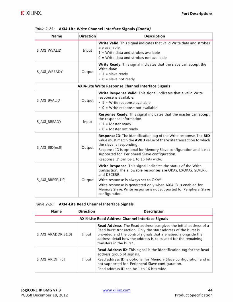
LogiCORE IP BMG v7.3 www.xilinx.com 44PG058 December 18, 2012 Product Specification
Port Descriptions
S_AXI_WVALID Input
Write Valid: This signal indicates that valid Write data and strobes are available: 1 = Write data and strobes available 0 = Write data and strobes not available
S_AXI_WREADY Output
Write Ready: This signal indicates that the slave can accept the Write data: • 1 = slave ready • 0 = slave not ready
AXI4-Lite Write Response Channel Interface Signals
S_AXI_BVALID Output
Write Response Valid: This signal indicates that a valid Write response is available: • 1 = Write response available • 0 = Write response not available
S_AXI_BREADY Input
Response Ready: This signal indicates that the master can accept the response information.• 1 = Master ready • 0 = Master not ready
S_AXI_BID[m:0] Output
Response ID: The identif ication tag of the Write response. The BID value must match the AWID value of the Write transaction to which the slave is responding.Response ID is optional for Memory Slave configuration and is not supported for Peripheral Slave configuration.Response ID can be 1 to 16 bits wide.
S_AXI_BRESP[1:0] Output
Write Response: This signal indicates the status of the Write transaction. The allowable responses are OKAY, EXOKAY, SLVERR, and DECERR.Write response is always set to OKAY.Write response is generated only when AXI4 ID is enabled for Memory Slave. Write response is not supported for Peripheral Slave configuration.
Table 2-26: AXI4-Lite Read Channel Interface Signals
Name Direction Description
AXI4-Lite Read Address Channel Interface Signals
S_AXI_ARADDR[31:0] Input
Read Address: The Read address bus gives the initial address of a Read burst transaction. Only the start address of the burst is provided and the control signals that are issued alongside the address detail how the address is calculated for the remaining transfers in the burst.
S_AXI_ARID[m:0] Input
Read Address ID: This signal is the identif ication tag for the Read address group of signals.Read address ID is optional for Memory Slave configuration and is not supported for Peripheral Slave configuration.Read address ID can be 1 to 16 bits wide.
Table 2-25: AXI4-Lite Write Channel Interface Signals (Cont’d)
Name Direction Description

LogiCORE IP BMG v7.3 www.xilinx.com 45PG058 December 18, 2012 Product Specification
Port Descriptions
S_AXI_ARVALID Input
Read Address Valid: This signal indicates, when HIGH, that the Read address and control information is valid and will remain stable until the address acknowledge signal, ARREADY, is high.1 = address and control information valid 0 = address and control information not valid
S_AXI_ARREADY Output
Read Address Ready: This signal indicates that the slave is ready to accept an address and associated control signals: 1 = slave ready 0 = slave not ready
AXI4-Lite Read Data Channel Interface Signals
S_AXI_RDATA[m-1:0] OutputRead Data: For Memory Slave configurations, the Read data bus can be 32 or 64 bits wide. For Peripheral Slave configurations, the Read data bus can be 8, 16, 32 or 64 bits wide.
S_AXI_RRESP[1:0] Output
Read Response: This signal indicates the status of the Read transfer. The allowable responses are OKAY, EXOKAY, SLVERR, and DECERR.Read response is always set to OKAY.Read response is generated only when AXI4 ID is enabled for Memory Slave. Read response is not supported for Peripheral Slave configuration.
S_AXI_RID[m:0] Output
Read ID Tag: This signal is the ID tag of the Read data group of signals. The RID value is generated by the slave and must match the ARID value of the Read transaction to which it is responding.Read ID tag is optional for Memory Slave configuration and is not supported for Peripheral Slave configuration.Read ID tag can be 1 to 16 bits wide.
S_AXI_RVALID Output
Read Valid: This signal indicates that the required Read data is available and the Read transfer can complete: 1 = Read data available 0 = Read data not available
S_AXI_RREADY Input
Read Ready: This signal indicates that the master can accept the Read data and response information: 1= Master ready 0 = Master not ready
Table 2-26: AXI4-Lite Read Channel Interface Signals (Cont’d)
Name Direction Description
LogiCORE IP BMG v7.3 www.xilinx.com 46PG058 December 18, 2012
Chapter 3
Designing with the CoreThis chapter describes the steps required to turn a Block memory Generator core into a fully functioning design integrated with the user application logic. It is important to note that depending on the configuration of the BMG core, only a subset of the implementation details provided are applicable. The guidelines in this chapter provide details about creating the most successful implementation of the core.
General Design GuidelinesThe Block Memory Generator is used to build custom memory modules from block RAM primitives in Xilinx FPGAs. The core implements an optimal memory by arranging block RAM primitives based on user selections, automating the process of primitive instantiation and concatenation. Using the CORE Generator Graphical User Interface (GUI), users can configure the core and rapidly generate a highly optimized custom memory solution.
Memory TypeThe Block Memory Generator creates f ive memory types: Single-port RAM, Simple Dual-port RAM, True Dual-port RAM, Single-port ROM, and Dual-port ROM. Figure 3-1 through Figure 3-5 illustrate the signals available for each type. Optional pins are displayed in italics.
For each configuration, optimizations are made within the core to minimize the total resources used. For example, a Simple Dual-port RAM with symmetric ports can utilize the special Simple Dual-port RAM primitive in Virtex-5 devices, which can save as much as f ifty percent of the block RAM resources for memories 512 words deep or fewer. The Single-port ROM allows Read access to the memory space through a single port, as illustrated in Figure 3-1.

LogiCORE IP BMG v7.3 www.xilinx.com 47PG058 December 18, 2012
General Design Guidelines
The Dual-port ROM allows Read access to the memory space through two ports, as shown in Figure 3-2.
The Single-port RAM allows Read and Write access to the memory through a single port, as shown in Figure 3-3.
X-Ref Target - Figure 3-1
Figure 3-1: Single-port ROM
X-Ref Target - Figure 3-2
Figure 3-2: Dual-port ROM
Single-Port ROM
ADDRA
ENA
RSTA
CLKA
DOUTA
REGCEA
Dual-Port ROM
ADDRA
ENA
RSTA
CLKA
DOUTA
DOUTB
REGCEA
ADDRB
ENB
RSTB
CLKB
REGCEB

LogiCORE IP BMG v7.3 www.xilinx.com 48PG058 December 18, 2012
General Design Guidelines
The Simple Dual-port RAM provides two ports, A and B, as illustrated in Figure 3-4. Write access to the memory is allowed via port A, and Read access is allowed via port B.
Note: For Virtex family architectures, Read access is via port A and Write access is via port B.
The True Dual-port RAM provides two ports, A and B, as illustrated in Figure 3-5. Read and Write accesses to the memory are allowed on either port.
X-Ref Target - Figure 3-3
Figure 3-3: Single-port RAM
X-Ref Target - Figure 3-4
Figure 3-4: Simple Dual-port RAM
Single-Port RAM
ADDRA
DINA
ENA
WEA
RSTA
CLKA
DOUTA
REGCEA
Simple Dual-Port RAM
CLKA
DOUTBADDRB
ENB
RSTB
CLKB
REGCEB
ADDRA
DINA
ENA
RDADDRECC
DBITERR
INJECTDBITERR
INJECTSBITERR
SBITERR WEA

LogiCORE IP BMG v7.3 www.xilinx.com 49PG058 December 18, 2012
General Design Guidelines
Selectable Memory AlgorithmThe Block Memory Generator core arranges block RAM primitives according to one of three algorithms: the minimum area algorithm, the low power algorithm and the f ixed primitive algorithm.
Minimum Area Algorithm
The minimum area algorithm provides a highly optimized solution, resulting in a minimum number of block RAM primitives used, while reducing output multiplexing. Figure 3-6 shows two examples of memories built using the minimum area algorithm.
X-Ref Target - Figure 3-5
Figure 3-5: True Dual-port RAM
True Dual-Port RAM
ADDRA
DINA
ENA
WEA
RSTA
CLKA
DOUTA
DOUTB
REGCEA
ADDRB
DINB
ENB
WEB
RSTB
CLKB
REGCEB

LogiCORE IP BMG v7.3 www.xilinx.com 50PG058 December 18, 2012
General Design Guidelines
Note: In Spartan-6 devices, two 9K block RAMs are used for one 1Kx18.
In the f irst example, a 3kx16 memory is implemented using three block RAMs. While it may have been possible to concatenate three 1kx18 block RAMs in depth, this would require more output multiplexing. The minimum area algorithm maximizes performance in this way while maintaining minimum block RAM usage.
In the second example, a 5kx17 memory, further demonstrates how the algorithm can pack block RAMs efficiently to use the fewest resources while maximizing performance by reducing output multiplexing.
Low Power Algorithm
The low power algorithm provides a solution that minimizes the number of primitives enabled during a Read or Write operation. This algorithm is not optimized for area and may use more block RAMs and multiplexers than the minimum area algorithm. Figure 3-7 shows two examples of memories built using the low power algorithm.
X-Ref Target - Figure 3-6
Figure 3-6: Examples of the Minimum Area Algorithm
3kx16 memory
2kx9
1kx18
2kx9
5kx17 memory
4kx4 4kx4
2kx9
2kx9
1kx18
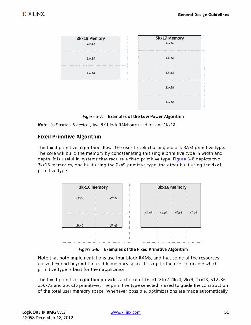
LogiCORE IP BMG v7.3 www.xilinx.com 51PG058 December 18, 2012
General Design Guidelines
Note: In Spartan-6 devices, two 9K block RAMs are used for one 1Kx18.
Fixed Primitive Algorithm
The fixed primitive algorithm allows the user to select a single block RAM primitive type. The core will build the memory by concatenating this single primitive type in width and depth. It is useful in systems that require a fixed primitive type. Figure 3-8 depicts two 3kx16 memories, one built using the 2kx9 primitive type, the other built using the 4kx4 primitive type.
Note that both implementations use four block RAMs, and that some of the resources utilized extend beyond the usable memory space. It is up to the user to decide which primitive type is best for their application.
The fixed primitive algorithm provides a choice of 16kx1, 8kx2, 4kx4, 2kx9, 1kx18, 512x36, 256x72 and 256x36 primitives. The primitive type selected is used to guide the construction of the total user memory space. Whenever possible, optimizations are made automatically
X-Ref Target - Figure 3-7
Figure 3-7: Examples of the Low Power Algorithm
X-Ref Target - Figure 3-8
Figure 3-8: Examples of the Fixed Primitive Algorithm
3kx16 Memory
1kx18
5kx17 Memory
1kx18
1kx18
1kx18
1kx18
1kx18
1kx18
1kx18
3kx16 memory
2kx9
2kx9
2kx9
2kx9
3kx16 memory
4kx4 4kx4 4kx4 4kx4
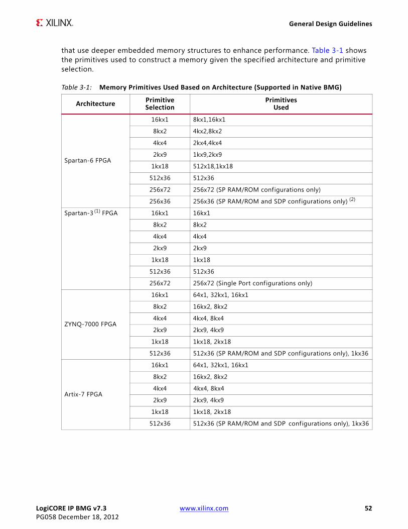
LogiCORE IP BMG v7.3 www.xilinx.com 52PG058 December 18, 2012
General Design Guidelines
that use deeper embedded memory structures to enhance performance. Table 3-1 shows the primitives used to construct a memory given the specif ied architecture and primitive selection.
Table 3-1: Memory Primitives Used Based on Architecture (Supported in Native BMG)
Architecture Primitive Selection
Primitives Used
Spartan-6 FPGA
16kx1 8kx1,16kx1
8kx2 4kx2,8kx2
4kx4 2kx4,4kx4
2kx9 1kx9,2kx9
1kx18 512x18,1kx18
512x36 512x36
256x72 256x72 (SP RAM/ROM configurations only)
256x36 256x36 (SP RAM/ROM and SDP configurations only) (2)
Spartan-3 (1) FPGA 16kx1 16kx1
8kx2 8kx2
4kx4 4kx4
2kx9 2kx9
1kx18 1kx18
512x36 512x36
256x72 256x72 (Single Port configurations only)
ZYNQ-7000 FPGA
16kx1 64x1, 32kx1, 16kx1
8kx2 16kx2, 8kx2
4kx4 4kx4, 8kx4
2kx9 2kx9, 4kx9
1kx18 1kx18, 2kx18
512x36 512x36 (SP RAM/ROM and SDP configurations only), 1kx36
Artix-7 FPGA
16kx1 64x1, 32kx1, 16kx1
8kx2 16kx2, 8kx2
4kx4 4kx4, 8kx4
2kx9 2kx9, 4kx9
1kx18 1kx18, 2kx18
512x36 512x36 (SP RAM/ROM and SDP configurations only), 1kx36

LogiCORE IP BMG v7.3 www.xilinx.com 53PG058 December 18, 2012
General Design Guidelines
Kintex-7 FPGA
16kx1 64x1, 32kx1, 16kx1
8kx2 16kx2, 8kx2
4kx4 4kx4, 8kx4
2kx9 2kx9, 4kx9
1kx18 1kx18, 2kx18
512x36 512x36 (SP RAM/ROM and SDP configurations only), 1kx36
256x72 512x72 (SP RAM/ROM and SDP configurations only)
Virtex-7 FPGA
16kx1 64x1, 32kx1, 16kx1
8kx2 16kx2, 8kx2
4kx4 4kx4, 8kx4
2kx9 2kx9, 4kx9
1kx18 1kx18, 2kx18
512x36 512x36 (SP RAM/ROM and SDP configurations only), 1kx36
256x72 512x72 (SP RAM/ROM and SDP configurations only)
Virtex-6 FPGA
16kx1 64x1, 32kx1, 16kx1
8kx2 16kx2, 8kx2
4kx4 4kx4, 8kx4
2kx9 2kx9, 4kx9
1kx18 1kx18, 2kx18
512x36 512x36 (SP RAM/ROM and SDP configurations only), 1kx36 (2)
256x72 512x72 (SP RAM/ROM and SDP configurations only)(2)
Virtex-5 FPGA 16kx1 64kx1, 32kx1, 16kx1
8kx2 16kx2, 8kx2
4kx4 8kx4, 4kx4
2kx9 4kx9, 2kx9
1kx18 2kx18, 1kx18
512x36 1kx36
256x72 512x72 (Single and Simple Dual-port RAMs and Single Port ROMs only)
Table 3-1: Memory Primitives Used Based on Architecture (Supported in Native BMG) (Cont’d)
Architecture Primitive Selection
Primitives Used
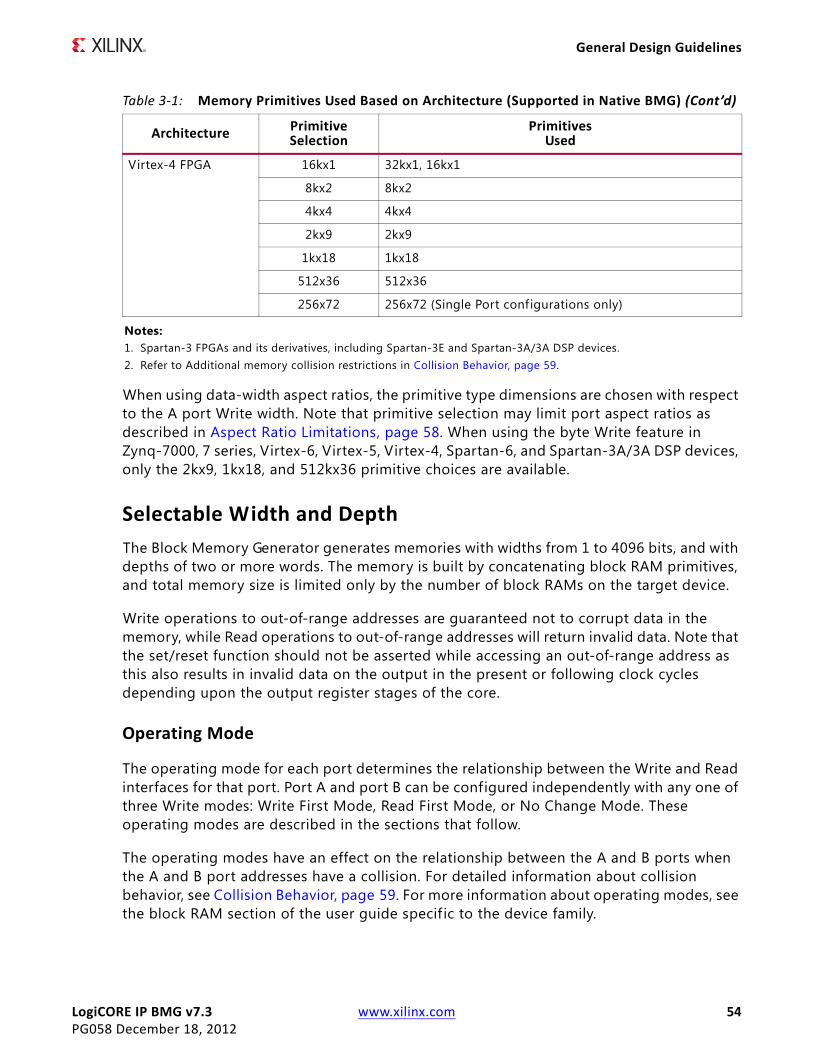
LogiCORE IP BMG v7.3 www.xilinx.com 54PG058 December 18, 2012
General Design Guidelines
When using data-width aspect ratios, the primitive type dimensions are chosen with respect to the A port Write width. Note that primitive selection may limit port aspect ratios as described in Aspect Ratio Limitations, page 58. When using the byte Write feature in Zynq-7000, 7 series, Virtex-6, Virtex-5, Virtex-4, Spartan-6, and Spartan-3A/3A DSP devices, only the 2kx9, 1kx18, and 512kx36 primitive choices are available.
Selectable Width and DepthThe Block Memory Generator generates memories with widths from 1 to 4096 bits, and with depths of two or more words. The memory is built by concatenating block RAM primitives, and total memory size is limited only by the number of block RAMs on the target device.
Write operations to out-of-range addresses are guaranteed not to corrupt data in the memory, while Read operations to out-of-range addresses will return invalid data. Note that the set/reset function should not be asserted while accessing an out-of-range address as this also results in invalid data on the output in the present or following clock cycles depending upon the output register stages of the core.
Operating Mode
The operating mode for each port determines the relationship between the Write and Read interfaces for that port. Port A and port B can be configured independently with any one of three Write modes: Write First Mode, Read First Mode, or No Change Mode. These operating modes are described in the sections that follow.
The operating modes have an effect on the relationship between the A and B ports when the A and B port addresses have a collision. For detailed information about collision behavior, see Collision Behavior, page 59. For more information about operating modes, see the block RAM section of the user guide specif ic to the device family.
Virtex-4 FPGA 16kx1 32kx1, 16kx1
8kx2 8kx2
4kx4 4kx4
2kx9 2kx9
1kx18 1kx18
512x36 512x36
256x72 256x72 (Single Port configurations only)
Notes: 1. Spartan-3 FPGAs and its derivatives, including Spartan-3E and Spartan-3A/3A DSP devices.2. Refer to Additional memory collision restrictions in Collision Behavior, page 59.
Table 3-1: Memory Primitives Used Based on Architecture (Supported in Native BMG) (Cont’d)
Architecture Primitive Selection
Primitives Used

LogiCORE IP BMG v7.3 www.xilinx.com 55PG058 December 18, 2012
General Design Guidelines
• Write First Mode: In WRITE_FIRST mode, the input data is simultaneously written into memory and driven on the data output, as shown in Figure 3-9. This transparent mode offers the flexibility of using the data output bus during a Write operation on the same port.
Note: The WRITE_FIRST operation is affected by the optional byte-Write feature in Zynq-7000, 7 series, Virtex-6, Virtex-5, Virtex-4, Spartan-6 and Spartan-3A/3A DSP devices. It is also affected by the optional Read-to-Write aspect ratio feature in Zynq-7000, 7 series, Virtex-6, Virtex-5 and Virtex-4 devices. For detailed information, see Write First Mode Considerations, page 59.
• Read First Mode: In READ_FIRST mode, data previously stored at the Write address appears on the data output, while the input data is being stored in memory. This Read-before-Write behavior is illustrated in Figure 3-10.
• No Change Mode: In NO_CHANGE mode, the output latches remain unchanged during a Write operation. As shown in Figure 3-11, the data output is still the previous Read data and is unaffected by a Write operation on the same port.
X-Ref Target - Figure 3-9
Figure 3-9: Write First Mode Example
X-Ref Target - Figure 3-10
Figure 3-10: Read First Mode Example
aa
WEA
DINA[15:0]
DOUTA[15:0]
CLKA
ADDRA bb
1111
ENA
cc dd
2222
MEM(aa) 1111 2222 MEM(dd)0000
DISABLED READWRITE
MEM(bb)=1111
WRITEMEM(cc)=
2222READ
aa
WEA
DINA[15:0]
DOUTA[15:0]
CLKA
ADDRA bb
1111
ENA
cc dd
2222
MEM(aa) old MEM(bb) old MEM(cc) MEM(dd)0000
DISABLED READWRITE
MEM(bb)=1111
WRITEMEM(cc)=
2222READ

LogiCORE IP BMG v7.3 www.xilinx.com 56PG058 December 18, 2012
General Design Guidelines
Data Width Aspect RatiosThe Block Memory Generator supports data width aspect ratios. This allows the port A data width to be different than the port B data width, as described in Port Aspect Ratios in the following section. In Zynq-7000, 7 series, Virtex-6, Virtex-5 and Virtex-4 FPGA-based memories, all four data buses (DINA, DOUTA, DINB, and DOUTB) can have different widths, as described in Zynq-7000, 7 Series, Virtex-6, Virtex-5 and Virtex-4 Read-to-Write Aspect Ratios, page 57.
The limitations of the data width aspect ratio feature (some of which are imposed by other optional features) are described in Aspect Ratio Limitations, page 58. The CORE Generator GUI ensures only valid aspect ratios are selected.
Port Aspect Ratios
The Block Memory Generator supports port aspect ratios of 1:32, 1:16, 1:8, 1:4, 1:2, 1:1, 2:1, 4:1, 8:1, 16:1, and 32:1. The port A data width can be up to 32 times larger than the port B data width, or vice versa. The smaller data words are arranged in little-endian format, as illustrated in Figure 3-12.
Port Aspect Ratio Example
Consider a True Dual-port RAM of 32x2048, which is the A port width and depth. From the perspective of an 8-bit B port, the depth would be 8192. The ADDRA bus is 11 bits, while the ADDRB bus is 13 bits. The data is stored little-endian, as shown in Figure 3-12. Note that An is the data word at address n, with respect to the A port. Bn is the data word at address n with respect to the B port. A0 is comprised of B3, B2, B1, and B0.
X-Ref Target - Figure 3-11
Figure 3-11: No Change Mode Example
aa
WEA
DINA[15:0]
DOUTA[15:0]
CLKA
ADDRA bb
1111
ENA
cc dd
2222
MEM(aa) MEM(dd)0000
DISABLED READWRITE
MEM(bb)=1111
WRITEMEM(cc)=
2222READ

LogiCORE IP BMG v7.3 www.xilinx.com 57PG058 December 18, 2012
General Design Guidelines
Zynq-7000, 7 Series, Virtex-6, Virtex-5 and Virtex-4 Read-to-Write Aspect Ratios
When implementing RAMs targeting Zynq-7000, 7 series, Virtex-6, Virtex-5 and Virtex-4 FPGAs, the Block Memory Generator allows Read and Write aspect ratios on either port. On each port A and port B, the Read to Write data width ratio of that port can be 1:32, 1:16, 1:8, 1:4, 1:2, 1:1, 2:1, 4:1, 8:1, 16:1, or 32:1.
Because the Read and Write interfaces of each port can differ, it is possible for all four data buses (DINA , DOUTA , DINB, and DOUTB) of True Dual-port RAMs to have a different width. For Single-port RAMs, DINA and DOUTA widths can be independent. The maximum ratio between any two data buses is 32:1. The widest data bus can be no larger than 4096 bits.
If the Read and Write data widths on a port are different, the memory depth is different with respect to Read and Write accesses. For example, if the Read interface of port A is twice as wide as the Write interface, then it is also half as deep. The ratio of the widths is always the inverse of the ratio of the depths. Because a single address bus is used for both the Write and Read interface of a port, the address bus must be large enough to address the deeper of the two depths. For the shallower interface, the least signif icant bits of the address bus are ignored. The data words are arranged in little-endian format, as illustrated in Figure 3-13.
Zynq-7000, 7 Series, Virtex-6, Virtex-5 and Virtex-4 Read-to-Write Aspect Ratio Example
Consider a True Dual-port RAM of 64x512, which is the port A Write width and depth. Table 3-2 defines the four data-port widths and their respective depths for this example.
The ADDRA width is determined by the larger of the A port depths (2048). For this reason, ADDRA is 11 bits wide. On port A, Read operations utilize the entire ADDRA bus, while Write operations ignore the least signif icant 2 bits.
X-Ref Target - Figure 3-12
Figure 3-12: Port Aspect Ratio Example Memory Map
Table 3-2: Read-to-Write Aspect Ratio Example Ports
Interface Data Width Memory Depth
Port A Write 64 512
Port A Read 16 2048
Port B Write 256 128
Port B Read 32 1024
31 0
B3A0 =
.
.
.
7 0. .7 0. .7 0. .7 0. .
7 0. .7 0. .7 0. .7 0. .
B2 B1 B0
B7 B6 B5 B4A1 =

LogiCORE IP BMG v7.3 www.xilinx.com 58PG058 December 18, 2012
General Design Guidelines
In the same way, the ADDRB width is determined by the larger of the B port depths (1024). For this reason, ADDRB is 10 bits wide. On port B, Read operations utilize the entire ADDRB bus, while Write operations ignore the least significant 3 bits.
The memory map in Figure 3-13 shows how port B Write words are related to port A Write words, in a little-endian arrangement. Note that AWn is the Write data word at address n with respect to port A, while BWn is the Write data word at address n with respect to port B.
BW0 is made up of AW3, AW2, AW1, and AW0. In the same way, BR0 is made up of AR1 and AR0, and AW0 is made up of BR1 and BR0. In the example above, the largest data width ratio is port B Write words (256 bits) to port A Read words (16 bits); this ratio is 16:1.
Aspect Ratio Limitations
In general, no port data width can be wider than 4096 bits, and no two data widths can have a ratio greater than 32:1. However, the following optional features further limit data width aspect ratios:
• Byte-writes: When using byte-writes, no two data widths can have a ratio greater than 4:1.
• Fixed primitive algorithm: When using the fixed primitive algorithm with an N-bit wide primitive, aspect ratios are limited to 32:N and 1:N from the port A Write width. For example, using the 4kx4 primitive type, the other ports may be no more than 8 times (32:4) larger than port A Write width and no less than 4 times (1:4) smaller.
Byte-WritesThe Block Memory Generator provides byte-Write support in Zynq-7000, 7 series, Virtex-6, Virtex-5, Virtex-4, Spartan-6, and Spartan-3A/3A DSP devices. Byte-writes are available using either 8-bit or 9-bit byte sizes. When using an 8-bit byte size, no parity bits are used and the memory width is restricted to multiples of 8 bits. When using a 9-bit byte size, each byte includes a parity bit, and the memory width is restricted to multiples of 9 bits.
When byte-writes are enabled, the WE[A|B] (WEA or WEB) bus is N bits wide, where N is the number of bytes in DIN[A|B]. The most signif icant bit in the Write enable bus corresponds to the most signif icant byte in the input word. Bytes will be stored in memory only if the corresponding bit in the Write enable bus is asserted during the Write operation.
X-Ref Target - Figure 3-13
Figure 3-13: Read-to-Write Aspect Ratio Example Memory Map
BW0 =
.
.
.
BW1 =
255 0
AW3 AW2 AW1
AW7 AW6 AW5 AW4
AW0

LogiCORE IP BMG v7.3 www.xilinx.com 59PG058 December 18, 2012
General Design Guidelines
When 8-bit bytes are selected, the DIN and DOUT data buses are constructed from 8-bit bytes, with no parity. When 9-bit bytes are selected, the DIN and DOUT data buses are constructed from 9-bit bytes, with the 9th bit of each byte in the data word serving as a parity bit for that byte.
The byte-Write feature may be used in conjunction with the data width aspect ratios, which may limit the choice of data widths as described in Data Width Aspect Ratios, page 56. However, it may not be used with the NO_CHANGE operating mode. This is because if a memory configuration uses multiple primitives in width, and only one primitive is being written to (using partial byte writes), then the NO_CHANGE mode only applies to that single primitive. The NO_CHANGE mode does not apply to the other primitives that are not being written to, so these primitives can still be read. The byte-Write feature also affects the operation of WRITE_FIRST mode, as described in Write First Mode Considerations, page 59.
Byte-Write Example
Consider a Single-port RAM with a data width of 24 bits, or 3 bytes with byte size of 8 bits. The Write enable bus, WEA, consists of 3 bits. Figure 3-14 illustrates the use of byte-writes, and shows the contents of the RAM at address 0. Assume all memory locations are initialized to 0.
Write First Mode ConsiderationsWhen performing a Write operation in WRITE_FIRST mode, the concurrent Read operation shows the newly written data on the output of the core. However, when using the byte-Write feature in Zynq-7000, 7 series, Virtex-6, Virtex-5, Virtex-4, Spartan-6, and Spartan-3A/3A DSP devices or the Read-to-Write aspect ratio feature in Zynq-7000, 7 series, Virtex-6, Virtex-5 and Virtex-4 devices, the output of the memory cannot be guaranteed.
Collision BehaviorThe Block Memory Generator core supports Dual-port RAM implementations. Each port is equivalent and independent, yet they access the same memory space. In such an arrangement, is it possible to have data collisions. The ramifications of this behavior are described for both asynchronous and synchronous clocks below.
X-Ref Target - Figure 3-14
Figure 3-14: Byte-Write Example
WEA[2:0]
DINA[23:0]
RAM Contents
CLKA
ADDRA[15:0]
b011
FF EE DD
0000
CC BB AA 33 22 11 00 FF 0099 88 77 66 55 44
b010 b101 b000 b110 b010
00 EE DD 00 BB DD 33 22 77 33 FF 7799 BB 77
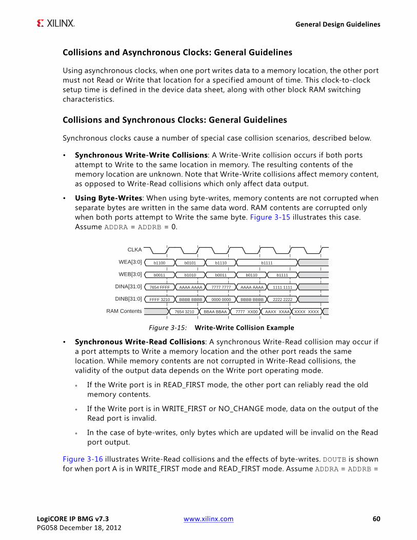
LogiCORE IP BMG v7.3 www.xilinx.com 60PG058 December 18, 2012
General Design Guidelines
Collisions and Asynchronous Clocks: General Guidelines
Using asynchronous clocks, when one port writes data to a memory location, the other port must not Read or Write that location for a specified amount of time. This clock-to-clock setup time is defined in the device data sheet, along with other block RAM switching characteristics.
Collisions and Synchronous Clocks: General Guidelines
Synchronous clocks cause a number of special case collision scenarios, described below.
• Synchronous Write-Write Collisions: A Write-Write collision occurs if both ports attempt to Write to the same location in memory. The resulting contents of the memory location are unknown. Note that Write-Write collisions affect memory content, as opposed to Write-Read collisions which only affect data output.
• Using Byte-Writes: When using byte-writes, memory contents are not corrupted when separate bytes are written in the same data word. RAM contents are corrupted only when both ports attempt to Write the same byte. Figure 3-15 illustrates this case. Assume ADDRA = ADDRB = 0.
• Synchronous Write-Read Collisions: A synchronous Write-Read collision may occur if a port attempts to Write a memory location and the other port reads the same location. While memory contents are not corrupted in Write-Read collisions, the validity of the output data depends on the Write port operating mode.
° If the Write port is in READ_FIRST mode, the other port can reliably read the old memory contents.
° If the Write port is in WRITE_FIRST or NO_CHANGE mode, data on the output of the Read port is invalid.
° In the case of byte-writes, only bytes which are updated will be invalid on the Read port output.
Figure 3-16 illustrates Write-Read collisions and the effects of byte-writes. DOUTB is shown for when port A is in WRITE_FIRST mode and READ_FIRST mode. Assume ADDRA = ADDRB =
X-Ref Target - Figure 3-15
Figure 3-15: Write-Write Collision Example
7777 XX00
WEA[3:0]
DINB[31:0]
RAM Contents
CLKA
b1100
DINA[31:0]
WEB[3:0] b0011
b0101
b1010
b1110
b0011
b1111
b0110 b1111
7654 3210 BBAA BBAA AAXX XXAA XXXX XXXX
FFFF 3210 BBBB BBBB 0000 0000 BBBB BBBB 2222 2222
7654 FFFF AAAA AAAA 7777 7777 AAAA AAAA 1111 1111

LogiCORE IP BMG v7.3 www.xilinx.com 61PG058 December 18, 2012
General Design Guidelines
0, port B is always reading, and all memory locations are initialized to 0. The RAM contents are never corrupted in Write-Read collisions.
Collisions and Simple Dual-port RAM
For Simple Dual-port RAM, the operating modes are not selectable, but are automatically set to either READ_FIRST or WRITE_FIRST depending on the target device family and clocking configuration (synchronous or asynchronous). The Simple Dual-port RAM is like a true dual-port RAM where only the Write interface of the A port and the Read interface of B port are connected. The operating modes define the Write-to-Read relationship of the A or B ports, and only impact the relationship between A and B ports during an address collision.
For Synchronous Clocking and during a collision, the Write mode of port A can be configured so that a Read operation on port B either produces data (acting like READ_FIRST), or produces undefined data (Xs). For this reason, the core is hard-coded to produce READ_FIRST-like behavior when configured as a Simple Dual-port RAM. For detailed information about this behavior, see Collision Behavior, page 59.
Exceptions: For Zynq-7000, 7 series, Virtex-6, and Spartan-6 devices, the operating mode (READ_FIRST or WRITE_FIRST respectively) is determined by whether the clocking mode selection is Synchronous (Common Clock) or Asynchronous. See Clocking Options: Select the Common Clock option when the clock (CLKA and CLKB) inputs are driven by the same clock buffer. in Chapter 7 for more details.
Additional Memory Collision Restrictions: Address Space Overlap
Virtex-6 and Spartan-6 FPGA block RAM memories have additional collision restrictions in the following configurations:
• When configured as True Dual Port (TDP)
• When CLKA (port A) and CLKB (port B) are Asynchronous
• In applications that perform a simultaneous Read and Write
X-Ref Target - Figure 3-16
Figure 3-16: Write-Read Collision Example
00XX 00XX
WEA[3:0]
DOUTBAWF
RAM Contents
CLKA
b0000
DINA[31:0]
b0101 b0000 b1100 b1111
3322 00AA
AAAA AAAA 3322 1100 1111 1111
0000 0000
DOUTBARF 0000 0000 00AA 00AA
00AA 00AA 00AA
3322 00AA
b0000
1111 1111
1111 1111
1111 111100AA 00AA0000 0000
XXXX XXXX XXXX

LogiCORE IP BMG v7.3 www.xilinx.com 62PG058 December 18, 2012
General Design Guidelines
• When either port A, port B, or both ports are configured with Write Mode configured as READ_FIRST
When using TDP Memory with Write Mode = READ_FIRST (TDP-RF mode) in conjunction with asynchronous clocking, see the “Conflict Avoidance” section of the 7 Series FPGAs Memory Resources User Guide (UG473), the Virtex-6 FPGA Memory Resources User Guide (UG363) or the Spartan-6 FPGA Block RAM Resources User Guide (UG383).
For Virtex-6 and Spartan-6 devices using the TDP-RF mode, the Address Space Overlap issue must be considered.
Optional Output RegistersThe Block Memory Generator allows optional output registers, which may improve the performance of the core. The user may choose to include register stages at two places: at the output of the block RAM primitives and at the output of the core.
Registers at the output of the block RAM primitives reduce the impact of the clock-to-out delay of the primitives. Registers at the output of the core isolate the delay through the output multiplexers, improving the clock-to-out delay of the Block Memory Generator core. Each of the two optional register stages can be chosen for port A and port B separately. Note that each optional register stage used adds an additional clock cycle of latency to the Read operation.
Figure 3-17 shows a memory configuration with registers at the output of the memory primitives and at the output of the core for one of the ports.

LogiCORE IP BMG v7.3 www.xilinx.com 63PG058 December 18, 2012
General Design Guidelines
For Zynq-7000, 7 series, Virtex-6, Virtex-5, Virtex-4, Spartan-6, and Spartan-3A DSP FPGAs, the Register Port [A|B] Output of Memory Primitives option may be implemented using the embedded block RAM registers, requiring no further FPGA resources. All other register stages are implemented in FPGA fabric. Figure 3-18 shows an example of a Zynq-7000, 7 series, Virtex-6, Virtex-5 or Virtex-4 FPGA-based memory that has been configured using both output register stages for one of the ports.
X-Ref Target - Figure 3-17
Figure 3-17: Spartan-3 Block Memory: Register Port [A|B] Outputs of Memory Primitives and Memory Core Options Enabled
Block Memory Generator Core
Latches
Latches
ENREGCE
MUX
Block RAM Primitives
Block RAM
CLK
RST
DOUT
S* : The synchronous reset (S) of the flop is gated by CE
Block RAM
Block RAM
Latches
CE
S*
D Q
CE
D Q
CE
D Q
CE
D Q
FALSE
Use REGCE Pin
TRUE
Primitive Output Registers
Core Output Registers
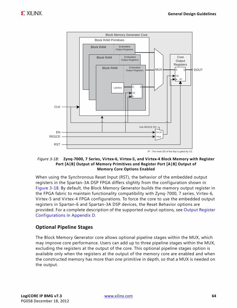
LogiCORE IP BMG v7.3 www.xilinx.com 64PG058 December 18, 2012
General Design Guidelines
When using the Synchronous Reset Input (RST), the behavior of the embedded output registers in the Spartan-3A DSP FPGA differs slightly from the configuration shown in Figure 3-18. By default, the Block Memory Generator builds the memory output register in the FPGA fabric to maintain functionality compatibility with Zynq-7000, 7 series, Virtex-6, Virtex-5 and Virtex-4 FPGA configurations. To force the core to use the embedded output registers in Spartan-6 and Spartan-3A DSP devices, the Reset Behavior options are provided. For a complete description of the supported output options, see Output Register Configurations in Appendix D.
Optional Pipeline Stages
The Block Memory Generator core allows optional pipeline stages within the MUX, which may improve core performance. Users can add up to three pipeline stages within the MUX, excluding the registers at the output of the core. This optional pipeline stages option is available only when the registers at the output of the memory core are enabled and when the constructed memory has more than one primitive in depth, so that a MUX is needed on the output.
X-Ref Target - Figure 3-18
Figure 3-18: Zynq-7000, 7 Series, Virtex-6, Virtex-5, and Virtex-4 Block Memory with Register Port [A|B] Output of Memory Primitives and Register Port [A|B] Output of
Memory Core Options Enabled
Block Memory Generator Core
CoreOutput
RegistersLatches
Latches
FALSE
Block RAM Primitives
Block RAM EmbeddedOutput Registers
Latches
CE
SS
R*
Block RAM EmbeddedOutput Registers
Latches
CE
SS
R*
Block RAM EmbeddedOutput Registers
Latches
EN
Use REGCE Pin
REGCE
MUX
CLK
RST
DOUT
CE
D Q
CE
R*
D Q
R* : The reset (R) of the flop is gated by CE
TRUE

LogiCORE IP BMG v7.3 www.xilinx.com 65PG058 December 18, 2012
General Design Guidelines
The pipeline stages are common for port A and port B and can be a value of 1, 2, or 3 if the Register Output of Memory Core option is selected in the GUI for both port A and port B. Note that each pipeline stage adds an additional clock cycle of latency to the Read operation.
If the configuration has BuiltIn_ECC (ECC), the SBITERR and DBITERR outputs are delayed to align with DOUT. Note that adding pipeline stages within the MUX improves performance only if the critical path in the design is the data through the MUX. The MUX size displayed in the GUI can be used to determine the number of pipeline stages to use within the MUX. See Optional Output Registers in Chapter 7 for detailed information. Figure 3-19 shows a memory configuration with an 8:1 MUX and two pipeline stages within the MUX. In the f igure, the 8:1 MUX is pipelined internally with two register stages.
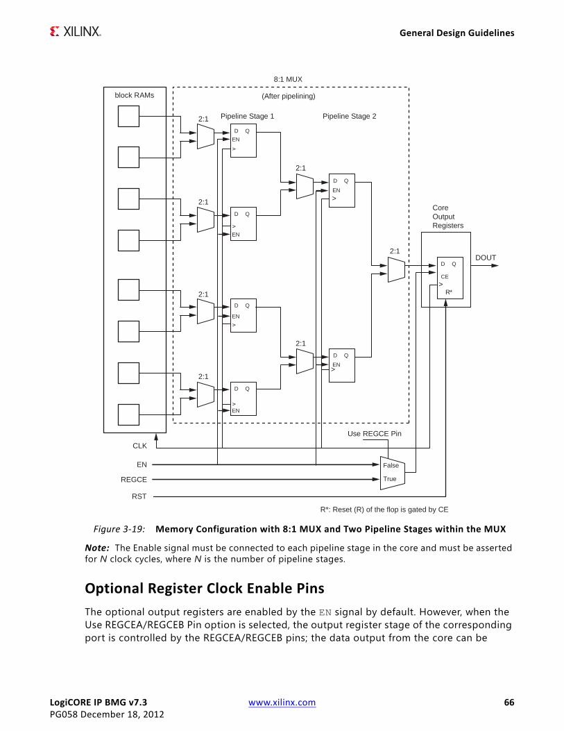
LogiCORE IP BMG v7.3 www.xilinx.com 66PG058 December 18, 2012
General Design Guidelines
Note: The Enable signal must be connected to each pipeline stage in the core and must be asserted for N clock cycles, where N is the number of pipeline stages.
Optional Register Clock Enable PinsThe optional output registers are enabled by the EN signal by default. However, when the Use REGCEA/REGCEB Pin option is selected, the output register stage of the corresponding port is controlled by the REGCEA/REGCEB pins; the data output from the core can be
X-Ref Target - Figure 3-19
Figure 3-19: Memory Configuration with 8:1 MUX and Two Pipeline Stages within the MUX
D Q
D Q
D Q
D Q
2:1
2:1
2:1
2:1
2:1
2:1
2:1
D Q
>
D Q
>
D Q CE
> R*
DOUT
block RAMs
Pipeline Stage 1 Pipeline Stage 2
8:1 MUX
(After pipelining)
Use REGCE Pin
REGCE
RST
CLK
EN
CoreOutputRegisters
False
True
R*: Reset (R) of the flop is gated by CE
vv
vv
EN
EN
EN
EN
EN
EN

LogiCORE IP BMG v7.3 www.xilinx.com 67PG058 December 18, 2012
General Design Guidelines
controlled independent of the flow of data through the rest of the core. When using the REGCE pin, the last output register operates independent of the EN signal.
Optional Set/Reset PinsThe set/reset pins (RSTA and RSTB) control the reset operation of the last register in the output stage. For memories with no output registers, the reset pins control the memory output latches.
When RST and REGCE are asserted on a given port, the data on the output of that port is driven to the reset value defined in the CORE Generator GUI. (The reset occurs on RST and EN when the Use REGCE Pin option is not selected.)
• For Virtex-4 FPGAs, if the option to use the set/reset pin is selected in conjunction with memory primitive registers and without core output registers, the Virtex-4 embedded block RAM registers are not utilized for the corresponding port and are implemented in the FPGA logic instead.
• For Zynq-7000, 7 series, Virtex-6, Spartan-6, and Spartan-3A DSP FPGAs, the set/reset behavior differs when the reset behavior option is selected. However, this option saves resources by using the embedded output registers available in the Spartan-6 and Spartan-3A DSP primitives. See Special Reset Behavior, page 69 for more information.
Memory Output Flow ControlThe combination of the enable (EN), reset (RST), and register enable (REGCE) pins allow a wide range of data flows in the output stage. Figure 3-20 and Figure 3-21 are examples on how this can be accomplished. Keep in mind that the RST and REGCE pins apply only to the last register stage.
Figure 3-20 depicts how RST can be used to control the data output to allow only intended data through. Assume that both output registers are used for port A, the port A reset value is 0xFFFF, and that EN and REGCE are always asserted. The data on the block RAM memory latch is labeled LATCH, while the output of the block RAM embedded register is labeled REG1. The output of the last register is the output of the core, DOUT.
X-Ref Target - Figure 3-20
Figure 3-20: Flow Control Using RST
REG1
CLKA
ADDRA[7:0] AA BB CC
data(AA) data(BB)
RST
LATCH data(AA) data(BB) data(CC)
DOUT data(AA) data(BB)
DD
FFFFFFFF
data(CC)
data(DD)
data(CC) FFFF
data(DD)

LogiCORE IP BMG v7.3 www.xilinx.com 68PG058 December 18, 2012
General Design Guidelines
Figure 3-21 depicts how REGCE can be used to latch the data output to allow only intended data through. Assume that only the memory primitive registers are used for port A, and that EN is always asserted and RST is always deasserted. The data on the block RAM memory latch is labeled latch, while the output of the last register, the block RAM embedded register, is the core output, DOUT.
Reset Priority
For Zynq-7000, 7 series, Virtex-6, and Spartan-6 devices, the Block Memory Generator core provides the option to choose the reset priority of the output stages of the Block Memory. In previous architectures such as Spartan-3A DSP and Virtex-5 devices, EN had a fixed priority over SSR (Synchronous Set Reset) for the memory latch, and REGCE (Register Clock Enable) had a f ixed priority over SSR for embedded registers.
In Spartan-6 devices, when a user chooses the Reset Priority as CE, then the enable signal (ENA or ENB) has a priority over the reset signal (RSTA or RSTB) for the memory latch, and the CE signal (REGCEA or REGCEB) has a priority over the reset signal for the output registers. When Reset Priority is chosen as SR, then the reset signal has a priority over the enable signal and the CE signal, in the case of the latch and output registers respectively.
In Zynq-7000, 7 series, and Virtex-6 devices, reset priority can be set only for the output registers and not for the memory latch. When CE is the selected priority, then CE (REGCEA or REGCEB) has a priority over reset (RSTA or RSTB). When SR is the selected reset priority, then reset has a priority over CE.
Figure 3-22 illustrates the reset behavior when the Reset Priority option is set to CE. Here, the first reset operation occurs successfully because EN is high, but the second reset operation does not cause any change in output because EN is low.
X-Ref Target - Figure 3-21
Figure 3-21: Flow Control Using REGCE
CLKA
ADDRA[7:0] AA BB CC
REGCE
LATCH data(AA) data(BB) data(CC)
DOUT data(AA) data(BB)
DD
data(DD)
data(CC) data(DD)

LogiCORE IP BMG v7.3 www.xilinx.com 69PG058 December 18, 2012
General Design Guidelines
Figure 3-23 illustrates the reset behavior when the Reset Priority option is set to SR. Here, reset is not dependent on enable and both reset operations occur successfully.
Special Reset Behavior
For Zynq-7000, 7 series, Virtex-6, Spartan-6, and Spartan-3A DSP devices, the Block Memory Generator provides the option to reset both the memory latch and the embedded primitive output register. This Reset Behavior option is available to users when they choose to have a primitive output register, but no core output register. When a user chooses the option to Reset the Memory Latch besides the primitive output register, then the reset value is asserted at the output for two clock cycles. However, when the user does not choose the option to Reset the Memory Latch in the presence of a primitive output register, the reset value is asserted at the output for only one clock cycle, since only the primitive output register is reset.
Note that the duration of reset assertion specif ied here is the minimum duration when the latch and register are always enabled, and the RST input is held high for only one clock cycle. If the enable signals are de-asserted or the RST input is held high for more than one clock cycle, the reset value may be asserted at the output for a longer duration.
In Zynq-7000, 7 series, and Virtex-6 devices, the latch and the embedded output register can be reset independently using two separate inputs (RSTREG and RSTRAM) that are
X-Ref Target - Figure 3-22
Figure 3-22: Reset Behavior When Reset Priority is Set to CE
X-Ref Target - Figure 3-23
Figure 3-23: Reset Behavior When Reset Priority is Set to SR
CLKA
aa bb cc dd ee
0000 MEM(aa) INIT_VAL MEM(cc)
ENA
RSTA
ADDRA
DOUTA[15:0]
Disabled Read Reset WhenENA=’1’
Read No ResetWhen EN=’0’
CLKA
aa bb cc dd ee
0000 MEM(aa) INIT_VAL
ENA
RSTA
ADDRA
DOUTA[15:0]
NoOperation
Read Reset Read Reset
MEM(cc) INIT_VAL
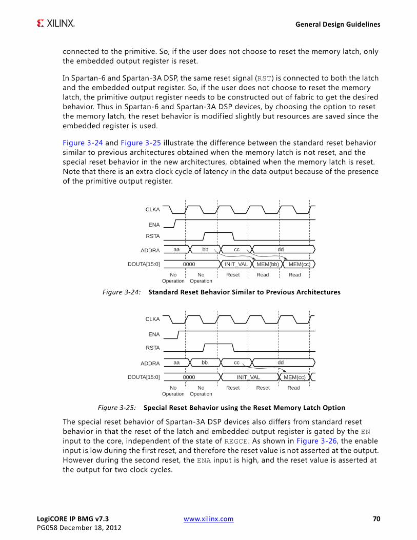
LogiCORE IP BMG v7.3 www.xilinx.com 70PG058 December 18, 2012
General Design Guidelines
connected to the primitive. So, if the user does not choose to reset the memory latch, only the embedded output register is reset.
In Spartan-6 and Spartan-3A DSP, the same reset signal (RST) is connected to both the latch and the embedded output register. So, if the user does not choose to reset the memory latch, the primitive output register needs to be constructed out of fabric to get the desired behavior. Thus in Spartan-6 and Spartan-3A DSP devices, by choosing the option to reset the memory latch, the reset behavior is modif ied slightly but resources are saved since the embedded register is used.
Figure 3-24 and Figure 3-25 illustrate the difference between the standard reset behavior similar to previous architectures obtained when the memory latch is not reset, and the special reset behavior in the new architectures, obtained when the memory latch is reset. Note that there is an extra clock cycle of latency in the data output because of the presence of the primitive output register.
The special reset behavior of Spartan-3A DSP devices also differs from standard reset behavior in that the reset of the latch and embedded output register is gated by the EN input to the core, independent of the state of REGCE. As shown in Figure 3-26, the enable input is low during the f irst reset, and therefore the reset value is not asserted at the output. However during the second reset, the ENA input is high, and the reset value is asserted at the output for two clock cycles.
X-Ref Target - Figure 3-24
Figure 3-24: Standard Reset Behavior Similar to Previous ArchitecturesX-Ref Target - Figure 3-25
Figure 3-25: Special Reset Behavior using the Reset Memory Latch Option
CLKA
aa bb cc
0000 MEM(bb)
ENA
RSTA
ADDRA
DOUTA[15:0]
NoOperation
NoOperation
Read ReadReset
INIT_VAL
dd
MEM(cc)
CLKA
aa bb cc
0000 INIT_VAL
ENA
RSTA
ADDRA
DOUTA[15:0]
NoOperation
NoOperation
Reset ReadReset
MEM(cc)
dd

LogiCORE IP BMG v7.3 www.xilinx.com 71PG058 December 18, 2012
General Design Guidelines
In Zynq-7000, 7 series, Virtex-6, and Spartan-6 devices, the reset of the memory latch is gated by EN, and the reset of the embedded register is gated by CE, similar to other architectures. As shown in Figure 3-27, both ENA and REGCEA are high at the time of the f irst reset, and the reset value is asserted at the output for two clock cycles. At the time of the second reset, ENA is high, but REGCEA is low; so the reset value does not appear at the output. At the time of the third reset, only REGCEA is high; so the reset value is asserted at the output for only one clock cycle.
Asynchronous Reset
The Spartan-6 device architecture provides the ability to asynchronously reset the memory latch and embedded output register. The Block Memory Generator core extends this capability to the core output registers and the primitive output registers constructed out of fabric. The GUI provides the option to choose between the two reset types: synchronous and asynchronous. When using an asynchronous reset, the reset value is asserted immediately when the reset input goes high, but is deasserted only at the following clock edge when reset is low and enable is high. Figure 3-28 illustrates an asynchronous reset operation in Spartan-6 devices.
X-Ref Target - Figure 3-26
Figure 3-26: Reset Gated by EN in Spartan-3A DSP Devices with the Reset Memory Latch Option
X-Ref Target - Figure 3-27
Figure 3-27: Reset Gated by CE in Zynq-7000, 7 Series, Virtex-6, and Spartan-6 Devices with Reset Memory Latch Option
bb
DOUTA[15:0]
CLKA
ADDRA
ENA
INIT_VAL0000
NOOPERATION READ RESETREAD
aa
READ
cc dd
RSTA
REGCE
MEM(aa)
ee
RESETNO
OPERATION
bb
DOUTA[15:0]
CLKA
ADDRA
0000
aa cc dd
RSTA
INIT_VAL MEM(bb)
ee
NOOPERATION RESET READREAD READREAD
ENA
REGCEA
RESET
MEM(dd)
READ
INIT_VAL
RESET

LogiCORE IP BMG v7.3 www.xilinx.com 72PG058 December 18, 2012
General Design Guidelines
Controlling Reset Operations in Zynq-7000, 7 Series, Virtex-6, and Spartan-6 FPGAs
The reset operation in Zynq-7000, 7 series, Virtex-6, and Spartan-6 devices is dependent on the following generics:
• Use RST[A|B] Pin: These options determine the presence or absence of RST pins at the output of the core.
• Reset Memory Latch (for Port A and Port B): This option determines if the memory latch will be reset in addition to the embedded primitive output register for the respective port.
• Reset Priority (for Port A and Port B): This option determines the priority of clock enable over reset or reset over clock enable for the respective port.
• Reset Type: This option determines if the reset is synchronous or asynchronous in Spartan-6 devices.
In addition to the above options, the options of output registers also affects reset functionality, since the option to reset the memory latch depends on these options. Table 3-3 lists the dependency of the reset behavior for Zynq-7000, 7 series, Virtex-6, and Spartan-6 devices on these parameters. In these configurations, the core output register does not exist. The reset behavior detailed in Table 3-3 uses Port A as an example. The reset behavior for Port B is identical.
X-Ref Target - Figure 3-28
Figure 3-28: Asynchronous Reset
CLKA
aa bb cc dd ee
0000 MEM(aa) INIT_VAL
ENA
RSTA
ADDRA
DOUTA[15:0]
NoOperation
Read Reset Read Reset
MEM(cc) MEM(dd)

LogiCORE IP BMG v7.3 www.xilinx.com 73PG058 December 18, 2012
General Design Guidelines
Table 3-3: Control of Reset Behavior in Zynq-7000, 7 Series, Virtex-6, and Spartan-6 for Single Port
Use
RSTA
Pin
Regi
ster
Por
t A O
utpu
t of
Mem
ory
Prim
itive
s
Rese
t Mem
ory
Latc
h
Rese
t Prio
rity
for P
ort A
Rese
t Typ
e (S
part
an-6
Onl
y)
S6 RESET BEHAVIOR V6 RESET BEHAVIOR
0 X X X X No control over reset No control over reset
1 0
(cannot be
selected)
“CE”, “SR”
“SYNC”, “ASYNC
”
Since no primitive output register exists, the reset applies only to the latch. Reset occurs synchronously or asynchronously depending on the Reset Type option, and is dependent or independent of the input enable signal based upon the Reset Priority. The reset value is asserted for only one clock cycle (only if input RST signal is high for only one clock and EN is high continuously).
Since no primitive output register exists, the reset applies only to the latch. For Zynq-7000, 7 series, and Virtex-6, the priority of SR cannot be set for the latch. Therefore, reset occurs synchronously when the enable input is ‘1’. The reset value is asserted for only one clock cycle (only if input RST signal is high for only one clock and EN is high continuously).
1 1 0 “CE”“SYNC”, “ASYNC
”
Fabric register used. Reset occurs synchronously or asynchronously depending on the Reset Type option, and is dependent or independent of the input enable signal based on the Reset Priority. Reset value asserted for one clock cycle (only if input RST signal is high for only one clock and REGCE is high continuously).
For Zynq-7000, 7 series, and Virtex-6 devices, the priority cannot be set for the latch. Therefore reset priority of “SR” is not supported.Reset occurs synchronously, and is dependent or independent of the input enable signal. Reset value asserted for one clock cycle (only if input RST signal is high for only one clock and REGCE is high continuously).

LogiCORE IP BMG v7.3 www.xilinx.com 74PG058 December 18, 2012
General Design Guidelines
1 1 1 “CE”, “SR”
“SYNC”, “ASYNC
”
Both memory latch and embedded output register of primitive are reset. Reset occurs synchronously or asynchronously depending on the Reset Type option, and is dependent or independent of the input enable signal based upon the Reset Priority. Reset value is asserted for at least two clock cycles when enable inputs of both stages are ‘1’, and may be more depending on the input RST and enable signals. If RST is asserted when the latch EN input is ‘1’ and the register enable input is ‘0’, the memory latch alone gets reset and this reset value gets output only when the register enable goes high.
For Zynq-7000, 7 series, and Virtex-6 devices, the priority cannot be set for the latch. Therefore reset priority of “SR” is not supported. Both memory latch and embedded output register of primitive are reset. Reset occurs synchronously at both these stages, and is dependent or independent of the input enable signal. Reset value is asserted for at least two clock cycles when enable inputs of both stages are ‘1’, and may be more depending on the input RST and enable signals. If RST is asserted when the latch EN input is ‘1’ and the register enable input is ‘0’, the memory latch alone gets reset and this reset value gets output only when the register enable goes high.
1 1 0 “SR”“SYNC”, “ASYNC
”
Fabric register used. Reset occurs synchronously or asynchronously when the RST input is ‘1’, irrespective of the state of the enable input.However, the reset value will get deasserted synchronously only once the enable input is ‘1’.
Not applicable.
Table 3-3: Control of Reset Behavior in Zynq-7000, 7 Series, Virtex-6, and Spartan-6 for Single Port (Cont’d)
Use
RSTA
Pin
Regi
ster
Por
t A O
utpu
t of
Mem
ory
Prim
itive
s
Rese
t Mem
ory
Latc
h
Rese
t Prio
rity
for P
ort A
Rese
t Typ
e (S
part
an-6
Onl
y)
S6 RESET BEHAVIOR V6 RESET BEHAVIOR

LogiCORE IP BMG v7.3 www.xilinx.com 75PG058 December 18, 2012
General Design Guidelines
Built-in Error Correction Capability and Error InjectionFor Zynq-7000, 7 series, Virtex-6, and Virtex-5 devices, the Block Memory Generator core supports built-in Hamming Error Correction Capability (ECC) for the block RAM primitives. For device support, see Table 3-4. Each Write operation generates eight protection bits for every 64 bits of data, which are stored with the data in memory. These bits are used during each Read operation to correct any single-bit error, or to detect (but not correct) any double-bit error.
1 1 1 “SR”“SYNC”,“ASYNC
”
Reset occurs synchronously or asynchronously when the RST input is ‘1’, irrespective of the state of the enable input. However, the reset value will get deasserted synchronously when the latch and embedded register are enabled sequentially for at least one clock cycle each after the reset input is deasserted.
Not applicable.
1 X X “SR”, “CE” ASYNC
Reset occurs asynchronously when the RST input is ‘1’. Dependencies on the remaining options are as explained above.
Not applicable.
Table 3-4: Hard ECC Data width Support
Zynq-7000 7 Series Virtex-6 Virtex-5 Spartan-6
Block RAM Mode SDP Mode + Read First
SDP Mode + Read First
SDP Mode + Read First
SDP Mode + No Change n/a
Supported Data Widths ≥ 64 ≥ 64 ≥ 64 ≥ 64 n/a
Bit Error Insertion Support Yes Yes Yes No n/a
Table 3-3: Control of Reset Behavior in Zynq-7000, 7 Series, Virtex-6, and Spartan-6 for Single Port (Cont’d)
Use
RSTA
Pin
Regi
ster
Por
t A O
utpu
t of
Mem
ory
Prim
itive
s
Rese
t Mem
ory
Latc
h
Rese
t Prio
rity
for P
ort A
Rese
t Typ
e (S
part
an-6
Onl
y)
S6 RESET BEHAVIOR V6 RESET BEHAVIOR

LogiCORE IP BMG v7.3 www.xilinx.com 76PG058 December 18, 2012
General Design Guidelines
This operation is transparent to the user. Two status outputs (SBITERR and DBITERR) indicate the three possible Read results: no error, single error corrected, and double error detected. For single-bit errors, the Read operation does not correct the error in the memory array; it only presents corrected data on DOUT. BuiltIn_ECC is only available when the following options are chosen:
• Zynq-7000, 7 series, Virtex-6, and Virtex-5 FPGAs
• Simple Dual-port RAM memory type
When using BuiltIn_ECC, the Block Memory Generator constructs the memory from special primitives available in Zynq-7000, 7 series, Virtex-6, and Virtex-5 FPGA architectures. The BuiltIn_ECC memory block is 512x64, and is composed of two 18k block RAMs combined with dedicated BuiltIn_ECC encoding and decoding hardware. The 512x64 primitives are used to build memory suff icient for the desired user memory space.
The Zynq-7000, 7 series, Virtex-6, and Virtex-5 BuiltIn_ECC primitives calculate BuiltIn_ECC for a 64-bit wide data input. If the data width chosen by a user is not an integral multiple of 64 (for example, there are spare bits in any BuiltIn_ECC primitive), then a double-bit error (DBITERR) may indicate that one or more errors have occurred in the spare bits. So, the accuracy of the DBITERR signal cannot be guaranteed in this case. For example, if the user's data width is 32, then 32 bits of the primitive are left spare. If two of the spare bits are corrupted, the DBITERR signal would be asserted even though the actual user data is not corrupt.
When using BuiltIn_ECC, the following limitations apply:
• Byte-Write enable is not available
• All port widths must be identical
• For Virtex-5 devices, No Change Operating mode is supported, and for Zynq-7000, 7 series, Virtex-6, and Virtex-5 devices, Read First Operating Mode is supported
• Use RST[A|B] Pin and the Output Reset Value options are not available
• Memory Initialization is not supported
• No Algorithm selection is available
Figure 3-29 illustrates a typical Write and Read operation for a Zynq-7000, 7 series, Virtex-6, and Virtex-5 FPGA Block Memory Generator core in Simple Dual-port RAM mode with BuiltIn_ECC enabled, and no additional output registers.

LogiCORE IP BMG v7.3 www.xilinx.com 77PG058 December 18, 2012
General Design Guidelines
Error Injection
For Virtex-5, the Block Memory Generator core does not support the insertion of errors for correction by BuiltIn_ECC in simulation. For this reason, the simulated functionality of ECC is identical to non-ECC behavior with the SBITERR and DBITERR outputs always disabled.
Zynq-7000, 7 series, and Virtex-6 devices, however, support error injection through two new optional pins: INJECTSBITERR and INJECTDBITERR. Users can use these optional error injection pins as debug pins to inject single or double-bit errors into specif ic locations during Write operations. The user can then check the assertion of the SBITERR and DBITERR signals at the output of those addresses. The user has the option to have no error injection pins, or to have only one or both of the error injection pins.
The RDADDRECC output port indicates the address at which a SBITERR or DBITERR has occurred. The RDADDRECC port, the two error injection ports, and the two error output ports are optional and become available only when the BuiltIn_ECC option is chosen. If the BuiltIn_ECC feature is not selected by the user, the primitive's INJECTSBITERR and INJECTDBITERR ports are internally driven to '0', and the primitive's outputs SBITERR, DBITERR, and RDADDRECC are not connected externally.
Figure 3-30 shows the assertion of the SBITERR and DBITERR output signals when errors are injected through the error injection pins during a Write operation.
X-Ref Target - Figure 3-29
Figure 3-29: Read and Write Operation with BuiltIn_ECC in Zynq-7000, 7 Series, Virtex-6, and Virtex-5 FPGAs
WEA
DINA
CLKA, CLKB
ADDRA
ADDRB
DOUTB
DBITERR
SBITERR
ENB
ENA
1111 2222
aa
aa
00 1100

LogiCORE IP BMG v7.3 www.xilinx.com 78PG058 December 18, 2012
General Design Guidelines
When the INJECTSBITERR and INJECTDBITERR inputs are asserted together at the same time for the same address during a Write operation (as in the case of address 3 in Figure 3-30), the INJECTDBITERR input takes precedence, and only the DBITERR output is asserted for that address during a Read operation. The data output for this address is not corrected.
Soft Error Correction Capability and Error injectionThis section describes the implementation and usage of the Soft Error Correction Control (Soft ECC) module that is supported in the Block Memory Generator.
Overview
The Soft ECC module detects and corrects all single-bit errors in a code word consisting of up to 64 bits of data and up to eight parity bits. In addition, it detects double-bit errors in the data. This design uses Hamming code, which is an eff icient method for ECC operations.
X-Ref Target - Figure 3-30
Figure 3-30: Assertion of SBITERR and DBITERR Signals by Using Error Injection Pins
CLK
EN
NOOPERATION WRITE READ
WE
1ADDR 0 2 3 1 2 3 4
INJECTSBITERR
INJECTDBITERR
ADIN 0 B C D E F 9
DOUT 0 A B C A Bx Cx
SBITERR
DBITERR
WRITE WRITE READ READ READ
SBITERRCorrected
Data
DBITERRIncorrect
Data

LogiCORE IP BMG v7.3 www.xilinx.com 79PG058 December 18, 2012
General Design Guidelines
Features
• Supports Soft ECC for data widths less than or equal to 64 bits in Zynq-7000, 7 series, Virtex-6 and Spartan-6 devices
• Uses Hamming error code correction
° Single-bit errors are corrected
° Double-bit errors are detected
• Supports Simple Dual-port RAM memory type
• Supports optional Input and/or Output Registering stages
• Supported Block Memory Generator features include:
° Minimum Area, Fixed Primitive and Low Power Algorithms
° Mux Pipelining Stages
° Embedded Primitive Registers
° Core Output Registers
° Optional Enable Inputs
• Fully parameterized implementation enables optimization of resources
Details
Each Write operation generates between 4 and 8 protection bits for 1 to 64 bits of data, which are stored with the data in memory. These bits are used during each Read operation to correct any single-bit error, or to detect (but not correct) any double-bit error.
The two status outputs (SBITERR and DBITERR) indicate the three possible Read results: no error, single error corrected, and double error detected. For single-bit errors, the Read operation does not correct the error in the memory array; it only presents corrected data on DOUT.
When using Soft ECC, the Block Memory Generator can construct the memory from the available primitives in Zynq-7000, 7 series, Virtex-6, and Spartan-6 FPGA architectures. The Soft ECC feature is implemented as an overlay on top of the Block Memory Generator core. This allows users to select algorithm options and registering options in the core. When Soft ECC is selected, limited core options include:
• Byte-Write enable is not available
• All port widths must be identical
• Use RST[A|B] Pin and the Output Reset Value options are not available
• Memory Initialization is not supported

LogiCORE IP BMG v7.3 www.xilinx.com 80PG058 December 18, 2012
General Design Guidelines
The Soft ECC implementation is optimized to generate the core for different data widths, as shown in Table 3-5. For the selected data width, the number of check bits appended is shown in Table 3-6. The operation of appending the additional check bits for the given data width is done within the Block Memory Generator core and is transparent to the user.
Figure 3-31 illustrates the implementation of Soft ECC logic for the Block Memory Generator core. The implementation shown in Figure 3-31 is for 64 bits of data; the implementation is parameterized for other data widths.
Table 3-5: Soft ECC Data width Support
Spartan-6 Zynq-7000 Virtex-5 Virtex-6 7 Series
Block RAM mode SDP Mode SDP Mode No SDP Mode SDP Mode
Supported Data Widths ≤ 64 bits ≤ 64 bits n/a ≤ 64 bits ≤ 64 bits
Bit Error Insertion Support
Yes Yes n/a Yes Yes
Table 3-6: Memory Width Calculation for Selected User Data Width
User Input Data Width Added Check Bits Total Memory Width in Bits
1-4 4 5-8
5-11 5 10-16
12-26 6 18-32
27-57 7 34-64
58-64 8 66-72
X-Ref Target - Figure 3-31
Figure 3-31: Block Memory Generator with Soft ECC
Block Memory Generator With Soft ECC
FF
FF
Block Memory Generator
FF
FF
X
0000…….0011
ROR
0000…….0001
0000…….0000
CB1
CB2
CB3
CB4
CB5
CB6
CB7
CB8
Data [63:0]
Mask Generation
Error Reporting
Data[63:0]
CheckBits[7:0] Check
Bits[7:0]
DINA [71:0]
ADDRAWEAENA
ADDRBWEBREGCEB ADDRB
WEBREGCEB
SBITERRDBITERRRDADDRECC
INJECTSBITERRINJECTDBITERR
DINA [63:0]ADDRA
WEAENA
DINA [63:0]
DOUTB [63:0]
Single BitError Correction
DOUTB [71:0]
FF Optional Registering Stages X XORing Logic
FF
X
X
X
X
X
X
X
X
X
X
X
LUT
LUT
LUT
LUT
LUT
LUT
LUT
LUT

LogiCORE IP BMG v7.3 www.xilinx.com 81PG058 December 18, 2012
General Design Guidelines
The optional input and output registering stages can be enabled by setting the values of parameters register_porta_input_of_softecc and register_portb_output_of_softecc appropriately. These registers improve the performance of the Soft ECC logic. By default, the input and output registering stages are disabled.
With Soft ECC, both Zynq-7000, 7 series, Virtex-6, and Spartan-6 devices support error injection through two new optional pins: INJECTSBITERR and INJECTDBITERR. The error injection operation is performed on both data bits and added check bits. Users can use these optional error injection pins as debug pins to inject single or double-bit errors into specific locations during Write operations. Then, the user can check the assertion of the SBITERR and DBITERR signals at the output of those addresses. The user may select no error injection pins, one error injection pin or both.
The RDADDRECC output port indicates the address at which a single or double-bit error has occurred. The RDADDRECC port, the two error injection ports, and the two error output ports are optional and become available only when the Soft ECC option is chosen. If the Soft ECC feature is not selected, the outputs SBITERR, DBITERR, and RDADDRECC are not connected externally.
Parameters
• softecc: This parameter enables the Soft ECC logic for Zynq-7000, 7 series, Virtex-6, and Spartan-6 device families.
• register_porta_input_of_softecc: This parameter registers the input ports in the design.
• register_portb_output_of_softecc: This parameter registers the output ports in the design.
• use_error_injection_pins: This parameter enables single and/or double-bit error injection capability during Write operations
• error_injection_type: This parameter specif ies the type of the error injection done in the Soft ECC logic. The error injection type can be either “Single_Bit_Error_Injection” or “Double_Bit_Error_Injection” or “Single_and_Double_Bit_Error_Injection.”
Parameter - Port dependencies
• When the softecc parameter is enabled: SBITERR, DBITERR and RDADDRECC ports are made available on the IO interface.
• When the use_error_injection_pins parameter is enabled and “Single_Bit_Error_Injection” option is selected: INJECTSBITERR port is made available on the IO interface.
• When the use_error_injection_pins parameter is enabled and “Double_Bit_Error_Injection” option is selected: INJECTDBITERR port is made available on the IO interface
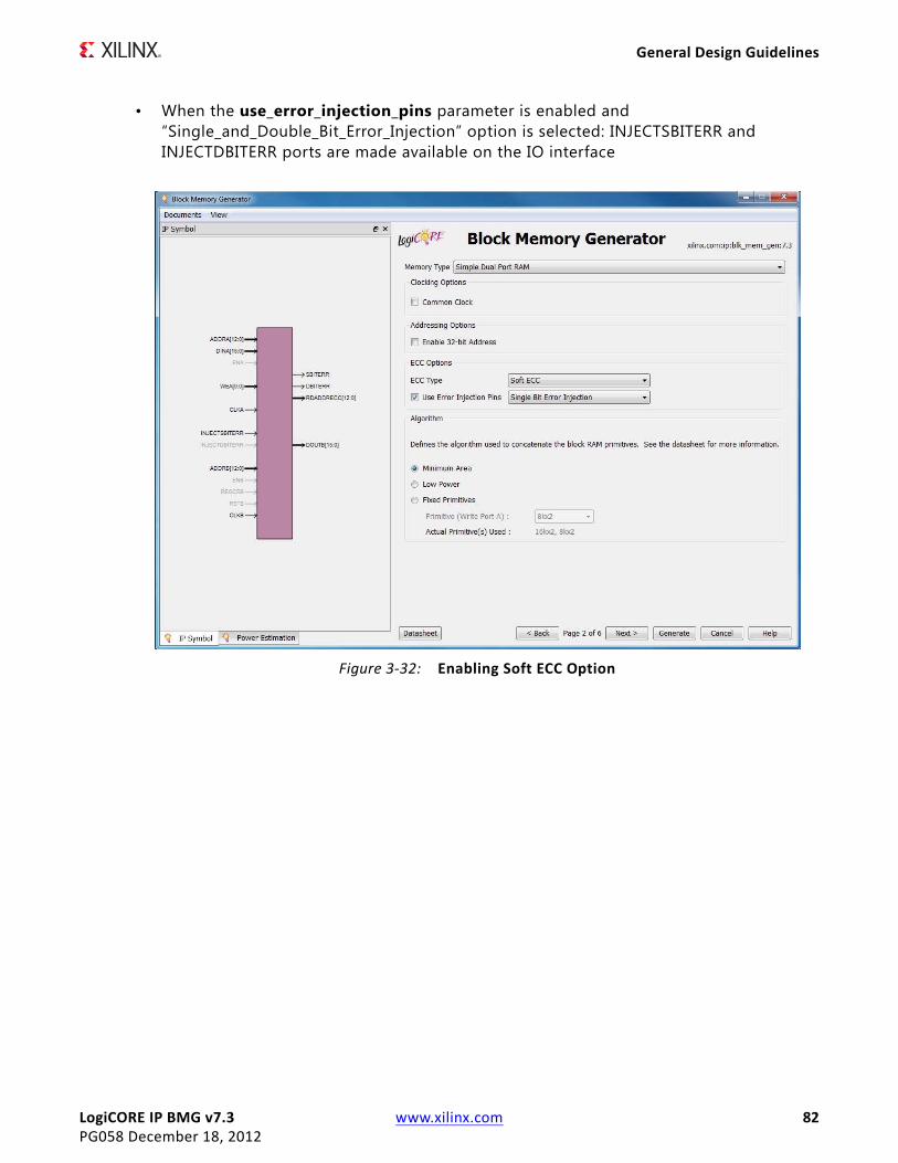
LogiCORE IP BMG v7.3 www.xilinx.com 82PG058 December 18, 2012
General Design Guidelines
• When the use_error_injection_pins parameter is enabled and “Single_and_Double_Bit_Error_Injection” option is selected: INJECTSBITERR and INJECTDBITERR ports are made available on the IO interface
X-Ref Target - Figure 3-32
Figure 3-32: Enabling Soft ECC Option

LogiCORE IP BMG v7.3 www.xilinx.com 83PG058 December 18, 2012
General Design Guidelines
Timing Diagrams
Figure 3-34 illustrates a typical Write and Read operation for Zynq-7000, 7 series, Virtex-6, and Spartan-6 devices for a core with a simple dual-port RAM configuration with Soft ECC enabled and no additional input or output registers.
X-Ref Target - Figure 3-33
Figure 3-33: Enabling Input/Output Registering Stages

LogiCORE IP BMG v7.3 www.xilinx.com 84PG058 December 18, 2012
General Design Guidelines
Figure 3-35 shows the assertion of the SBITERR and DBITERR output signals when errors are injected through the error injection pins during a Write operation.
X-Ref Target - Figure 3-34
Figure 3-34: Read and Write Operations with Soft ECC
X-Ref Target - Figure 3-35
Figure 3-35: Assertion of SBITERR and DBITERR Signals
WEA
DINA
CLKA, CLKB
ADDRA
ADDRB
DOUTB
DBITERR
SBITERR
ENB
ENA
1111 2222
aa
aa
00 1100
CLK
EN
NOOPERATION WRITE READ
WE
1ADDR 0 2 3 1 2 3 4
INJECTSBITERR
INJECTDBITERR
ADIN 0 B C D E F 9
DOUT 0 A B C A Bx Cx
SBITERR
DBITERR
WRITE WRITE READ READ READ
SBITERRCorrected
Data
DBITERRIncorrect
Data

LogiCORE IP BMG v7.3 www.xilinx.com 85PG058 December 18, 2012
General Design Guidelines
When the INJECTSBITERR and INJECTDBITERR inputs are asserted together at the same time for the same address during a Write operation (address 3 in Figure 3-35), then the INJECTDBITERR input takes precedence. Only the DBITERR output is asserted for that address during a Read operation. The data output for this address is not corrected.
Device Utilization and Performance Benchmarks
Table 3-7: Resource utilization for Spartan-6 Devices (XC6SLX25T-2CSG324)a b
a. Uses Fixed Primitive Algorithm (Primitive Configuration is 512x36).b. Memory type is SDP.
Depth xWidth Mode Check
Bits
Resource Utilizationc
c. No register stage.
Performanced
d. Uses Memory Core Output Register.
Block RAMs(52)
Slice LUTs(15032)
Slice Register(30064)
Max Freq(MHz)
1Kx8W/o ECC 2 4 0 221
With ECC 5 2 27 0 187
1Kx16W/o ECC 2 8 0 219
With ECC 6 2 61 0 201
1Kx32W/o ECC 2 16 0 209
With ECC 7 4 120 0 161
1Kx64W/o ECC 4 32 0 200
With ECC 8 4 231 0 121
Table 3-8: : Resource utilization for Virtex-6 Devices (XC6VLX75T-2FF784)a b
a. Uses Fixed Primitive Algorithm (Primitive Configuration is 1Kx36).b. Memory type is SDP.
Depth xWidth Mode Check
Bits
Resource Utilizationc
c. No register stage.
Performanced
d. Uses Memory Core Output Register.
Block RAMs(52)
Slice LUTs(15032)
Slice Register(30064)
Max Freq(MHz)
1Kx8W/o ECC 1 0 0 387
With ECC 5 1 24 0 385
1Kx16W/o ECC 1 0 0 391
With ECC 6 1 57 0 379
1Kx32W/o ECC 1 0 0 386
With ECC 7 2 112 0 350
1Kx64W/o ECC 2 0 0 370
With ECC 8 2 218 0 291

LogiCORE IP BMG v7.3 www.xilinx.com 86PG058 December 18, 2012
General Design Guidelines
Smaller Primitive Configurations in Spartan-6The introduction of the new 9K primitive in Spartan-6 results in smaller memory configurations: 8kx1, 4kx2, 2kx4, 1kx9, 512x18 and 256x36 (this primitive is only supported in SP and SDP configurations). In previous Spartan families, extra-wide configurations were only supported in Single Port memory configurations. The 9K primitive, RAMB8BWER, allows the primitive to be configured in either the TDP or the SDP mode. The presence of the SDP mode of operation allows the extra-wide 256x36 configuration, even for Simple Dual Port memory configurations.
Lower Data Widths in Zynq-7000, 7 Series, and Virtex-6 SDP ConfigurationsThe Zynq-7000, 7 series, and Virtex-6 FPGA architectures with the new SDP primitives support lower data widths than the Virtex-5 FPGAs. In Virtex-5 devices, the RAMB18SDP primitive could only support a symmetric configuration with port widths of 36, and the RAMB36SDP primitive could only support a symmetric configuration with port widths of 72. For Zynq-7000, 7 series, and Virtex-6 devices, new width combinations are possible for Port A and Port B, as shown in Table 3-9.
Table 3-9: Data Widths Supported by Zynq-7000, 7 series, and Virtex-6 SDP Primitives (1)(2)(3)
Primitive Read Port Width Write Port Width Read Port Width Write Port Width
RAMB18 SDP Primitive
x1 x32 x32 x1
x2 x32 x32 x2
x4 x32 x32 x4
x9 x36 x36 x9
x18 x36 x36 x18
x36 x36 - -
RAMB36 SDP Primitive
x1 x64 x64 x1
x2 x64 x64 x2
x4 x64 x64 x4
x9 x72 x72 x9
x18 x72 x72 x18
x36 x72 x72 x36
x72 x72 - -
Notes: 1. Refer to Additional Memory Collision Restrictions: Address Space Overlap, page 61.2. The selection of SDP primitives depends on the algorithm selected.3. Asymmetric data widths cause the SDP to be not selected.

LogiCORE IP BMG v7.3 www.xilinx.com 87PG058 December 18, 2012
Clocking
ClockingThe Block Memory Generator core has two clocks: clka and clkb. Depending on the configuration, one or two clocks can be enabled.
ResetsThe Block Memory Generator core has two resets. Depending on the configuration, the core can have different reset operations as explained in Optional Set/Reset Pins, Reset Priority, Special Reset Behavior and Asynchronous Reset.
LogiCORE IP BMG v7.3 www.xilinx.com 88PG058 December 18, 2012
SECTION II: VIVADO DESIGN SUITE
Customizing and Generating the Core
Constraining the Core
Detailed Example Design

LogiCORE IP BMG v7.3 www.xilinx.com 89PG058 December 18, 2012
Chapter 4
Customizing and Generating the CoreThis chapter includes information on using Vivado tools to customize and generate the core.
For more details about getting started with the Vivado Design Suite, see the Vivado tools user guides.
GUIThe Block Memory Generator is available in the Vivado IP catalog. To open the Block Memory core, go to IP Catalog > Memories & Storage Elements > RAMs & ROMs.
The following section defines the possible customization options in the Block Memory Generator GUI screens. The actual GUI screens depend on the user configuration.
The Native interface Block Memory Generator GUI includes six main screens:
• Native Block Memory Generator First Screen
• Port Options Screen
• Other Options Screen
• Summary Screen
• Power Estimate Options Screen
• Interface Type Selection Screen
• AXI4 Interface Options Screen
In addition, all the screens share common tabs and buttons to provide information about the core and to navigate the Block Memory Generator GUI.
Native Block Memory Generator First ScreenThe main Block Memory Generator screen is used to define the component name and provides the Interface Options for the core.

LogiCORE IP BMG v7.3 www.xilinx.com 90PG058 December 18, 2012
GUI
• Interface Type
° Native: Implements a Native Block Memory Generator Core compatible with previously released versions of the Block Memory Generator.
• Memory Type: Select the type of memory to be generated.
° Single-port RAM
° Simple Dual-port RAM
° True Dual-port RAM
° Single-port ROM
° Dual-port ROM
• ECC Options: When targeting Zynq-7000, 7 series, Virtex-6, Virtex-5, and Spartan-6 devices, and when the Simple dual-port RAM memory type is selected, the ECC Type option becomes available. It provides the user the choice to select the type of ECC required.
° Built-In ECC: When targeting Zynq-7000, 7 series, Virtex-6 and Virtex-5 devices, and when the selected ECC Type is BuiltIn_ECC, the built-in Hamming Error Correction is
X-Ref Target - Figure 4-1
Figure 4-1: Block Memory Generator Main Screen

LogiCORE IP BMG v7.3 www.xilinx.com 91PG058 December 18, 2012
GUI
enabled for the Zynq-7000, 7 series, Virtex-6, and Virtex-5 FPGA architecture.
For the Zynq-7000, 7 series, and Virtex-6 FPGA, the Use Error Injection Pins option is available for selection if the ECC option is selected. This option enables error injection pins. On choosing this option, additional options are available to have Single-Bit Error Injection (INJECTSBITERR), Double-Bit Error Injection (INJECTDBITERR), or both. See Hamming Error Correction Capability in Chapter 1 for more information.
When using ECC, the following limitations apply:
- Byte-Write Enable is not available.
- All port widths must be identical.
- For Virtex-5 devices, No Change Operating mode is supported. For Zynq-7000, 7 series, and Virtex-6 devices, Read First Operating Mode is supported.
- The Use RST[A|B] Pin and the Output Reset Value options are not available.
- Memory Initialization is not supported.
- No algorithm selection is available.
° Soft ECC: When targeting Zynq-7000, 7 series, Virtex-6, and Spartan-6 devices, and when the selected ECC Type is Soft_ECC, soft error correction (using Hamming code) is enabled for the Zynq-7000, 7 series, Virtex-6, and Spartan-6 FPGAs.
The Use Error Injection Pins option is available for selection if the Soft ECC option is selected. This option enables error injection pins. On choosing this option, additional options are available to have Single-Bit Error Injection (INJECTSBITERR), Double-Bit Error Injection (INJECTDBITERR), or both. See Soft Error Correction Capability and Error injection in Chapter 3 for more information about this option and the limitations that apply.
When using Soft ECC, the following conditions apply:
- Supports Soft ECC for data widths less than or equal to 64 bits
- Uses Hamming error code correction: Single-bit errors are corrected and double-bit errors are detected.
- Supports Simple Dual-port RAM memory type
- Supports optional Input and/or Output Registering stages
- Supported Block Memory Generator features include:
Minimum Area, Fixed Primitive and Low Power Algorithms
Mux Pipelining Stages

LogiCORE IP BMG v7.3 www.xilinx.com 92PG058 December 18, 2012
GUI
Embedded Primitive Registers
Core Output Registers
Optional Enable Inputs
- Fully parameterized implementation for optimized resource utilization
• Common Clock : Select the Common Clock option when the clock (CLKA and CLKB) inputs are driven by the same clock buffer.
IMPORTANT: For Zynq-7000, 7 series, Virtex-6, and Spartan-6 devices with COMMON_CLOCK selected, WRITE_MODE is set as READ_FIRST for Simple Dual Port RAM Memory type, otherwise WRITE_MODE is set as WRITE_FIRST.
• Write Enable: When targeting Zynq-7000, 7 series, Virtex-6, Virtex-5, Virtex-4, Spartan-6, and Spartan-3A/3A DSP devices, select whether to use the byte-Write enable feature. Byte size is either 8-bits (no parity) or 9-bits (including parity). The data width of the memory will be multiples of the selected byte-size.
• Algorithm: Select the algorithm used to implement the memory:
° Minimum Area Algorithm: Generates a core using the least number of primitives.
° Low Power Algorithm: Generates a core such that the minimum number of block RAM primitives are enabled during a Read or Write operation.
° Fixed Primitive Algorithm: Generates a core that concatenates a single primitive type to implement the memory. Choose which primitive type to use in the drop-down list.

LogiCORE IP BMG v7.3 www.xilinx.com 93PG058 December 18, 2012
GUI
Port Options Screen
• Memory Size: Specify the port [A|B] Write width and depth. Select the port [A|B] Read width from the drop-down list of valid choices. The Read depth is calculated automatically.
• Operating Mode: Specify the port [A|B] operating mode.
° READ_FIRST
° WRITE_FIRST
° NO_CHANGE
• Enable Port Type: Select the enable type:
° Always enabled (no ENA|ENB pin available)
° Use ENA|ENB pin
• Port [A|B] Optional Output Registers: Select the output register stages to include:
° Primitives Output Register: Select to insert output register after the memory primitives for port A and port B separately. When targeting Zynq-7000, 7 series, Virtex-6, Virtex-5 or Virtex-4 FPGAs, the embedded output registers in the block
X-Ref Target - Figure 4-2
Figure 4-2: Port A Options

LogiCORE IP BMG v7.3 www.xilinx.com 94PG058 December 18, 2012
GUI
RAM primitives are used if the user chooses to register the output of the memory primitives. For Spartan-6 and Spartan-3A DSP, either the primitive embedded registers or fabric registers from FPGA slices are used, depending upon the Reset Behavior option chosen by the user. For other architectures, the registers in the FPGA slices are used. Note that in Virtex-4 devices, the use of the RST input prevents the core from using the embedded output registers. See Output Register Configurations in Appendix D for more information.
° Core Output Register: Select for each port (A or B) to insert a register on the output of the memory core for that port. When selected, registers are implemented using FPGA slices to register the core's output.
° REGCE[A|B] Pin: Select to use a separate REGCEA or REGCEB input pin to control the enable of the last output register stage in the memory. When unselected, all register stages are enabled by ENA/ENB.
• Port [A|B] Output Reset Options
° Use RST[A|B] Pin (Set/Reset Pin): Choose whether a set/reset pin (RST[A|B]) is needed.
° Reset Priority: The Reset Priority option for each port is available only when the Use RST Pin option of the corresponding port is chosen. The user can set the reset priority to either CE or SR. For more information on the reset priority feature, see Reset Priority in Chapter 3.
° Reset Behavior: The Reset Behavior (Reset Memory Latch) options for each port are available only when the Use RST Pin option and the Register Output of Memory Primitives option of the corresponding port are chosen, and the Register Memory Core option of the corresponding port is not chosen.
° The Reset Memory Latch option modifies the behavior of the reset and changes the duration for which the reset value is asserted. The minimum duration of reset assertion is displayed as information in the GUI based upon the choice for this option. For more information on the Reset Memory Latch option, see Special Reset Behavior in Chapter 3.
° Output Reset Value (Hex): Specify the reset value of the memory output latch and output registers. These values are with respect to the Read port widths.

LogiCORE IP BMG v7.3 www.xilinx.com 95PG058 December 18, 2012
GUI
Other Options Screen
• Pipeline Stages within Mux: Available only when the Register Output of Memory Core option is selected for both port A and port B and when the constructed memory has more than one primitive in depth, so that a MUX is needed at the output. Select a value of 0, 1, 2, or 3 from the drop-down list.
The MUX size displayed in the GUI can be used to determine the number of pipeline stages to use within the MUX. Select the appropriate number of pipeline stages for your design based on the device architecture.
• Memory Initialization: Select whether to initialize the memory contents using a COE f ile, and whether to initialize the remaining memory contents with a default value. When using asymmetric port widths or data widths, the COE file and the default value are with respect to the port A Write width.
• Structural/UNISIM Simulation Model Options: Select the type of warning messages and outputs generated by the structural simulation model in the event of collisions. For the options of ALL, WARNING_ONLY and GENERATE_X_ONLY, the collision detection feature will be enabled in the UniSim models to handle collision under any condition.
X-Ref Target - Figure 4-3
Figure 4-3: Other Options Screen

LogiCORE IP BMG v7.3 www.xilinx.com 96PG058 December 18, 2012
GUI
The NONE selection is intended for designs that have no collisions and clocks (Port A and Port B) that are never in phase or within 3000 ps in skew. If NONE is selected, the collision detection feature will be disabled in the models, and the behavior during collisions is left for the simulator to handle. So, the output will be unpredictable if the clocks are in phase or from the same clock source or within 3000 ps in skew, and the addresses are the same for both ports. The option NONE is intended for design with clocks never in phase.
• Behavioral Simulation Model Options: Select the type of warning messages generated by the behavioral simulation model. Select whether the model should assume synchronous clocks (Common Clock) for collision warnings.
• Reset Type: The Reset Type option is available only for Spartan-6 devices and when either or both of Use RSTA Pin or Use RSTB Pin option are chosen. The user can set the reset type to either Synchronous or Asynchronous. For more information on this option, see Asynchronous Reset in Chapter 3.
Summary ScreenX-Ref Target - Figure 4-4
Figure 4-4: Summary Screen

LogiCORE IP BMG v7.3 www.xilinx.com 97PG058 December 18, 2012
GUI
Power Estimate Options Screen
The Power Estimation tab on the left side of the GUI screen shown in Figure 4-5 provides a rough estimate of power consumption for the core based on the configured Read width, Write width, clock rate, Write rate and enable rate of each port. The power consumption calculation assumes a toggle rate 50%. More accurate estimates can be obtained on the routed design using the XPower Analyzer tool. See www.xilinx.com/power for more information on the XPower Analyzer.
The screen has an option to provide "Additional Inputs for Power Estimation" apart from configuration parameters. The following parameters can be entered by the user for power calculation:
• Clock Frequency [A|B]: The operating clock frequency of the two ports A and B respectively.
• Write Rate [A|B]: Write rate of ports A and B respectively.
X-Ref Target - Figure 4-5
Figure 4-5: Power Estimate Options Screen
LogiCORE IP BMG v7.3 www.xilinx.com 98PG058 December 18, 2012
GUI
• Enable Rate [A|B]: Average access rate of port A and B respectively.
Information Section
This section displays an informational summary of the selected core options.
• Memory Type: Reports the selected memory type.
• Block RAM Resources: Reports the exact number of 9K, 18K and 36K block RAM primitives which will be used to construct the core.
• Total Port A Read Latency: The number of clock cycles for a Read operation for port A. This value is controlled by the optional output registers options for port A on the previous screen.
• Total Port B Read Latency: The number of clock cycles for a Read operation for port B. This value is controlled by the optional output registers options for port B on the previous screen.
• Address Width: The actual width of the address bus to each port.
Specifying Initial Memory Contents
The Block Memory Generator core supports memory initialization using a memory coeff icient (COE) file or the default data option in the CORE Generator GUI, or a combination of both.
The COE file can specify the initial contents of each memory location, while default data specifies the contents of all memory locations. When used in tandem, the COE file can specify a portion of the memory space, while default data f ills the rest of the remaining memory space. COE files and default data is formatted with respect to the port A Write width (or port A Read width for ROMs).
A COE is a text f ile which specif ies two parameters:
• memory_initialization_radix: The radix of the values in the memory_initialization_vector. Valid choices are 2, 10, or 16.
• memory_initialization_vector : Defines the contents of each memory element. Each value is LSB-justif ied and assumed to be in the radix defined by memory_initialization_radix.
The following is an example COE f ile. Note that semi-colon is the end of line character.
; Sample initialization file for a; 8-bit wide by 16 deep RAMmemory_initialization_radix = 16;memory_initialization_vector = 12, 34, 56, 78, AB, CD, EF, 12, 34, 56, 78, 90, AA, A5, 5A, BA;

LogiCORE IP BMG v7.3 www.xilinx.com 99PG058 December 18, 2012
GUI
Coefficients can be separated by a space, a comma, or by placing one value in each line with a carriage return.
Block RAM Usage
The Information panel (screen 5 of the Block Memory Generator GUI) reports the actual number of 9K, 18K and 36K block RAM blocks to be used.
To estimate this value when using the fixed primitive algorithm, the number of block RAM primitives used is equal to the width ratio (rounded up) multiplied by the depth ratio (rounded up), where the width ratio is the width of the memory divided by the width of the selected primitive, and the depth ratio is the depth of the memory divided by the depth of the primitive selected.
To estimate block RAM usage when using the low power algorithm requires a few more calculations:
• If the memory width is an integral multiple of the width of the widest available primitive for the chosen architecture, then the number of primitives used is calculated in the same way as the f ixed primitive algorithm. The width and depth ratios are calculated using the width and depth of the widest primitive. For example, for a memory configuration of 2kx72, the width ratio is 2 and the depth ratio is 4 using the widest primitive of 512x36. As a result, the total available primitives used is 8.
• If the memory width is greater than an integral multiple of the widest primitive, then in addition to the above calculated primitives, more primitives are needed to cover the remaining width. This additional number is obtained by dividing the memory depth by the depth of the additional primitive chosen to cover the remaining width. For example, a memory configuration of 17kx37 requires one 512x36 primitive to cover the width of 36, and an additional 16kx1 primitive to cover the remaining width of 1. To cover the depth of 17K, 34 512x36 primitives and 2 16kx1 primitives are needed. As a result, the total number of primitives used for this configuration is 36.
• If the memory width is less than the width of the widest primitive, then the smallest possible primitive that covers the memory width is chosen for the solution. The total number of primitives used is obtained by dividing the memory depth by the depth of the chosen primitive. For example, for a memory configuration of 2kx32, the chosen primitive is 512x36, and the total number of primitives used is 2k divided by 512, which is 4.
When using the minimum area algorithm, it is not as easy to determine the exact block RAM count. This is because the actual algorithms perform complex manipulations to produce optimal solutions. The optimistic estimate of the number of 18K block RAMs is total memory bits divided by 18k (the total number of bits per primitive) rounded up. Given that this algorithm packs block RAMs very eff iciently, this estimate is often very accurate for most memories.

LogiCORE IP BMG v7.3 www.xilinx.com 100PG058 December 18, 2012
Generating the AXI4 Interface Block Memory Generator Core
LUT Utilization and Performance
The LUT utilization and performance of the core are directly related to the arrangement of primitives and the selection of output registers. Particularly, the number of primitives cascaded in depth to implement a memory determines the size of the output multiplexer and the size of the input decoder, which are implemented in the FPGA fabric.
Note: Although the primary goal of the minimum area algorithm is to use the minimum number of block RAM primitives, it has a secondary goal of maximizing performance – as long as block RAM usage does not increase.
Generating the AXI4 Interface Block Memory Generator CoreThe AXI4 Interface Block Memory Generator GUI includes two additional screens followed by Native BMG configuration screens:
• Interface Type Selection Screen
• AXI4 Interface Options Screen
Interface Type Selection ScreenThe main Block Memory Generator screen is used to define the component name and provides the Interface Options for the core.

LogiCORE IP BMG v7.3 www.xilinx.com 101PG058 December 18, 2012
Generating the AXI4 Interface Block Memory Generator Core
Component Name
Base name of the output f iles generated for this core. The name must begin with a letter and be composed of the following characters: a to z, 0 to 9, and “_”.
• Interface Type:
° AXI4: Implements an AXI4 Interface Block Memory Generator Core.
X-Ref Target - Figure 4-6Interface Options for the core.
Figure 4-6: AXI4 Interface Selection Screen of Block Memory Generator

LogiCORE IP BMG v7.3 www.xilinx.com 102PG058 December 18, 2012
Generating the AXI4 Interface Block Memory Generator Core
AXI4 Interface Options Screen
• AXI4 Interface Options:
° AXI4: Implements an AXI4 Block Memory Generator Core.
° AXI4-Lite: Implements an AXI4-Lite Block Memory Generator Core.
• AXI4 Slave Options:
° Memory Slave: Implements a AXI4 Interface Block Memory Generator Core in Memory Slave mode
° Peripheral Slave: Implements a AXI4 Interface Block Memory Generator Core in Peripheral Slave mode
• ID Width Configurations:
° ID Width: When enabled supports AWID/BID/ARID/RID generation, ID Width can be configured from 1 to 16 bits
X-Ref Target - Figure 4-7
Figure 4-7: AXI4 Interface Options

LogiCORE IP BMG v7.3 www.xilinx.com 103PG058 December 18, 2012
Output Generation
Output GenerationThe output files generated from the Xilinx Vivado Design Suite are placed in the <project_directory> top-level directory. Depending on the settings, the f ile output list may include some or all of the following files:
<project_directory>/<project_name.data>Contains constraints and file set details.
<project directory>/<project_name>.src/sources_1/ip/<component name> Contains the sources like XCI, XDC, TCL and document f iles.
<component name>/synthContains the source f ile necessary to synthesize the Block Memory Generator
<component name>/simContains the source f ile necessary to synthesize the Block Memory Generator
<component name>/example_designContains the source f ile necessary to synthesize the example design
<component name>/simulationContains the source f ile necessary to simulate the example design
<component name>/simulation/functionalContains the scripts necessary to run functional simulation on the core including example design
<component name>/simulation/timingContains the scripts necessary to run timing simulation on the core including example design
The Block Memory Generator core directories and their associated files are defined in the following sections.
<project directory>/<project_name>.src/sources_1/ip/<component name> This directory contains templates for instantiation of the core, example design, synth, XML and the XCI f iles.
Table 4-1: Component Name Directory
Name Description
<component_name>.xci Log file from VIVADO software describing which options were used to generate the Block Memory Generator core. An XCI f ile can also be used as an input to the Vivado Design Suite.
<component_name>.{veo|vho} VHDL or Verilog instantiation template.
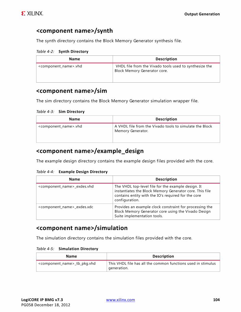
LogiCORE IP BMG v7.3 www.xilinx.com 104PG058 December 18, 2012
Output Generation
<component name>/synthThe synth directory contains the Block Memory Generator synthesis f ile.
<component name>/simThe sim directory contains the Block Memory Generator simulation wrapper f ile.
<component name>/example_designThe example design directory contains the example design f iles provided with the core.
<component name>/simulationThe simulation directory contains the simulation f iles provided with the core.
Table 4-2: Synth Directory
Name Description
<component_name>.vhd VHDL f ile from the Vivado tools used to synthesize the Block Memory Generator core.
Table 4-3: Sim Directory
Name Description
<component_name>.vhd A VHDL file from the Vivado tools to simulate the Block Memory Generator.
Table 4-4: Example Design Directory
Name Description
<component_name>_exdes.vhd The VHDL top-level f ile for the example design. It instantiates the Block Memory Generator core. This f ile contains entity with the IO’s required for the core configuration.
<component_name>_exdes.xdc Provides an example clock constraint for processing the Block Memory Generator core using the Vivado Design Suite implementation tools.
Table 4-5: Simulation Directory
Name Description
<component_name>_tb_pkg.vhd This VHDL f ile has all the common functions used in stimulus generation.

LogiCORE IP BMG v7.3 www.xilinx.com 105PG058 December 18, 2012
Output Generation
<component name>/simulation/functionalThe functional directory contains the scripts to launch XSIM/MIT Simulation with simulation test bench set as top entity.
<component name>/simulation/timingThe timing directory contains the scripts to launch XSIM/MTI Simulation with simulation test bench set as top entity.
<component_name>_tb_synth.vhd This VHDL f ile instantiates the example design.
<component_name>_tb.vhd This VHDL f ile is the top-level test bench File.
Table 4-6: Functional Directory
Name Description
Simulate_xsim.sh XSim macro f ile for Linux machines that compiles the example design sources and the structural simulation model. The demonstration test bench then runs the functional simulation to completion.
Simulate_xsim.bat XSim macro file for Windows that compiles the example design sources and the structural simulation model. The demonstration test bench then runs the functional simulation to completion.
wave_xsim.tcl XSim macro file that opens a Wave window with top-level signals.
simulate_mti.sh Linux shell script that executes the ModelSim macro f ile.
simulate_mti.bat Windows batch script that executes the ModelSim macro file.
simulate_mti.do A ModelSim macro f ile that compiles the HDL sources and runs the simulation.
Table 4-7: Timing Directory
Name Description
Simulate_xsim.sh XSim macro f ile for Linux machines that compiles the example design sources and the structural simulation model. The demonstration test bench then runs the functional simulation to completion.
Simulate_xsim.bat XSim macro file for Windows that compiles the example design sources and the structural simulation model. The demonstration test bench then runs the functional simulation to completion.
wave_xsim.tcl XSim macro file that opens a Wave window with top-level signals.
simulate_mti.sh Linux shell script that executes the ModelSim macro f ile.
simulate_mti.bat Windows batch script that executes the ModelSim macro file.
simulate_mti.do A ModelSim macro f ile that compiles the HDL sources and runs the simulation.
Table 4-5: Simulation Directory (Cont’d)
Name Description

LogiCORE IP BMG v7.3 www.xilinx.com 106PG058 December 18, 2012
Output Generation

LogiCORE IP BMG v7.3 www.xilinx.com 107PG058 December 18, 2012
Chapter 5
Constraining the CoreThis chapter contains details about constraining the core.
Required ConstraintsThere are no required constraints.
Device, Package, and Speed Grade SelectionsSee IP Facts for details about support devices.
Clock FrequenciesThis core can operate up-to 200 MHz with the maximum possible configuration on a Virtex-7 device.
Clock ManagementThe Block Memory Generator uses a CLKA,CLKB and ACLK and RSTA, RSTB and ARESETN based on the design configuration. The only constraints needed are clocking constraints.
Clock PlacementThe Block Memory Generator core does not have any special requirement on the placement of the clock.

LogiCORE IP BMG v7.3 www.xilinx.com 108PG058 December 18, 2012
Banking
BankingThere are no banking constraints.
Transceiver PlacementThere are no transceiver constraints.
I/O Standard and PlacementThere are no I/O constraints.
LogiCORE IP BMG v7.3 www.xilinx.com 109PG058 December 18, 2012
Chapter 6
Detailed Example DesignThis chapter contains details about the Block Memory Generator example design using the Vivado Design Suite.
Directory and File ContentsSee Output Generation in Chapter 4 for a detailed list of f iles generated with the example design.
Example DesignThe Block Memory Generator example design includes the following:
• HDL wrapper which instantiates the Block Memory Generator netlist
• Block Memory Generator constraint f ile
The Block Memory Generator example design has been tested with Vivado Design Suite v2012.4.

LogiCORE IP BMG v7.3 www.xilinx.com 110PG058 December 18, 2012
SECTION III: ISE DESIGN SUITE
Customizing and Generating the Core
Constraining the Core
Detailed Example Design

LogiCORE IP BMG v7.3 www.xilinx.com 111PG058 December 18, 2012
Chapter 7
Customizing and Generating the CoreThis chapter includes information on using Xilinx tools to customize and generate the core.
GUIThe Block Memory Generator is available from the CORE Generator software. To open the Block Memory core from the main CORE Generator window, do the following:
Click View by Function > Memories & Storage Elements > RAMs & ROMs
The following section defines the maximum possible customization options in the Block Memory Generator GUI screens. The actual GUI screens with enabled options will depend on the user configuration.
CORE Generator Parameter ScreensThe Native interface Block Memory Generator GUI includes six main screens:
• Interface Type Selection Screen
• Native Block Memory Generator First Screen
• Port Options Screen
• Output Registers and Memory Initialization Screen
• Reset Options Screen
• Simulation Model Options and Information Screen
In addition, all the screens share common tabs and buttons to provide information about the core and to navigate the Block Memory Generator GUI.
Interface Type Selection Screen
The main Block Memory Generator screen is used to define the component name and provides the Interface Options for the core.

LogiCORE IP BMG v7.3 www.xilinx.com 112PG058 December 18, 2012
GUI
• Component Name: Base name of the output f iles generated for this core. The name must begin with a letter and be composed of the following characters: a to z, 0 to 9, and “_”.
• Interface Type
° Native: Implements a Native Block Memory Generator Core compatible with previously released versions of the Block Memory Generator.
° AXI4: Implements an AXI4 Interface Block Memory Generator Core.
X-Ref Target - Figure 7-1
Figure 7-1: Interface Selection Screen
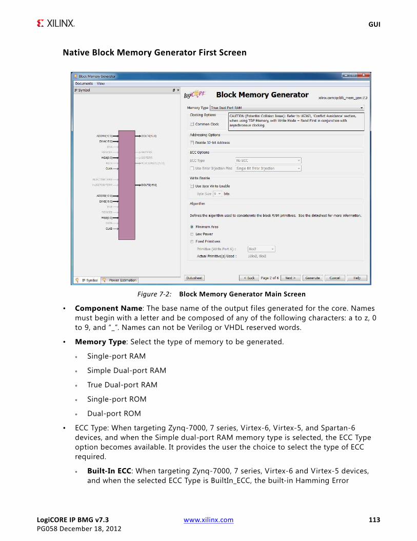
LogiCORE IP BMG v7.3 www.xilinx.com 113PG058 December 18, 2012
GUI
Native Block Memory Generator First Screen
• Component Name: The base name of the output files generated for the core. Names must begin with a letter and be composed of any of the following characters: a to z, 0 to 9, and “_”. Names can not be Verilog or VHDL reserved words.
• Memory Type: Select the type of memory to be generated.
° Single-port RAM
° Simple Dual-port RAM
° True Dual-port RAM
° Single-port ROM
° Dual-port ROM
• ECC Type: When targeting Zynq-7000, 7 series, Virtex-6, Virtex-5, and Spartan-6 devices, and when the Simple dual-port RAM memory type is selected, the ECC Type option becomes available. It provides the user the choice to select the type of ECC required.
° Built-In ECC: When targeting Zynq-7000, 7 series, Virtex-6 and Virtex-5 devices, and when the selected ECC Type is BuiltIn_ECC, the built-in Hamming Error
X-Ref Target - Figure 7-2
Figure 7-2: Block Memory Generator Main Screen

LogiCORE IP BMG v7.3 www.xilinx.com 114PG058 December 18, 2012
GUI
Correction is enabled for the Zynq-7000, 7 series, Virtex-6, and Virtex-5 FPGA architecture.
For the Zynq-7000, 7 series, and Virtex-6 FPGA, the Use Error Injection Pins option is available for selection if the ECC option is selected. This option enables error injection pins. On choosing this option, additional options are available to have Single-Bit Error Injection (INJECTSBITERR), Double-Bit Error Injection (INJECTDBITERR), or both. See Hamming Error Correction Capability in Chapter 1 for more information.
When using ECC, the following limitations apply:
- Byte-Write Enable is not available.
- All port widths must be identical.
- For Virtex-5 devices, No Change Operating mode is supported. For Zynq-7000, 7 series, and Virtex-6 devices, Read First Operating Mode is supported.
- The Use RST[A|B] Pin and the Output Reset Value options are not available.
- Memory Initialization is not supported.
- No algorithm selection is available.
° Soft ECC: When targeting Zynq-7000, 7 series, Virtex-6, and Spartan-6 devices, and when the selected ECC Type is Soft_ECC, soft error correction (using Hamming code) is enabled for the Zynq-7000, 7 series, Virtex-6, and Spartan-6 FPGAs.
The Use Error Injection Pins option is available for selection if the Soft ECC option is selected. This option enables error injection pins. On choosing this option, additional options are available to have Single-Bit Error Injection (INJECTSBITERR), Double-Bit Error Injection (INJECTDBITERR), or both. See Soft Error Correction Capability and Error injection in Chapter 3 for more information about this option and the limitations that apply.
When using Soft ECC, the following conditions apply:
- Supports Soft ECC for data widths less than or equal to 64 bits
- Uses Hamming error code correction: Single-bit errors are corrected and double-bit errors are detected.
- Supports Simple Dual-port RAM memory type
- Supports optional Input and/or Output Registering stages
- Supported Block Memory Generator features include:
Minimum Area, Fixed Primitive and Low Power Algorithms
Mux Pipelining Stages

LogiCORE IP BMG v7.3 www.xilinx.com 115PG058 December 18, 2012
GUI
Embedded Primitive Registers
Core Output Registers
Optional Enable Inputs
- Fully parameterized implementation for optimized resource utilization
• Clocking Options: Select the Common Clock option when the clock (CLKA and CLKB) inputs are driven by the same clock buffer.
IMPORTANT: For Zynq-7000, 7 series, Virtex-6, and Spartan-6 devices with COMMON_CLOCK selected, WRITE_MODE is set as READ_FIRST for Simple Dual Port RAM Memory type, otherwise WRITE_MODE is set as WRITE_FIRST.
• Write Enable: When targeting Zynq-7000, 7 series, Virtex-6, Virtex-5, Virtex-4, Spartan-6, and Spartan-3A/3A DSP devices, select whether to use the byte-Write enable feature. Byte size is either 8-bits (no parity) or 9-bits (including parity). The data width of the memory will be multiples of the selected byte-size.
• Algorithm: Select the algorithm used to implement the memory:
° Minimum Area Algorithm: Generates a core using the least number of primitives.
° Low Power Algorithm: Generates a core such that the minimum number of block RAM primitives are enabled during a Read or Write operation.
° Fixed Primitive Algorithm: Generates a core that concatenates a single primitive type to implement the memory. Choose which primitive type to use in the drop-down list.

LogiCORE IP BMG v7.3 www.xilinx.com 116PG058 December 18, 2012
GUI
Port Options Screen
Port A Options
• Memory Size: Specify the port A Write width and depth. Select the port A Read width from the drop-down list of valid choices. The Read depth is calculated automatically.
° Operating Mode: Specify the port A operating mode.
- READ_FIRST
- WRITE_FIRST
- NO_CHANGE
° Enable: Select the enable type:
- Always enabled (no ENA pin available)
- Use ENA pin
Port B Options
• Memory Size: Select the port B Write and Read widths from the drop-down list of valid choices. The Read depth is calculated automatically.
X-Ref Target - Figure 7-3
Figure 7-3: Port A Options
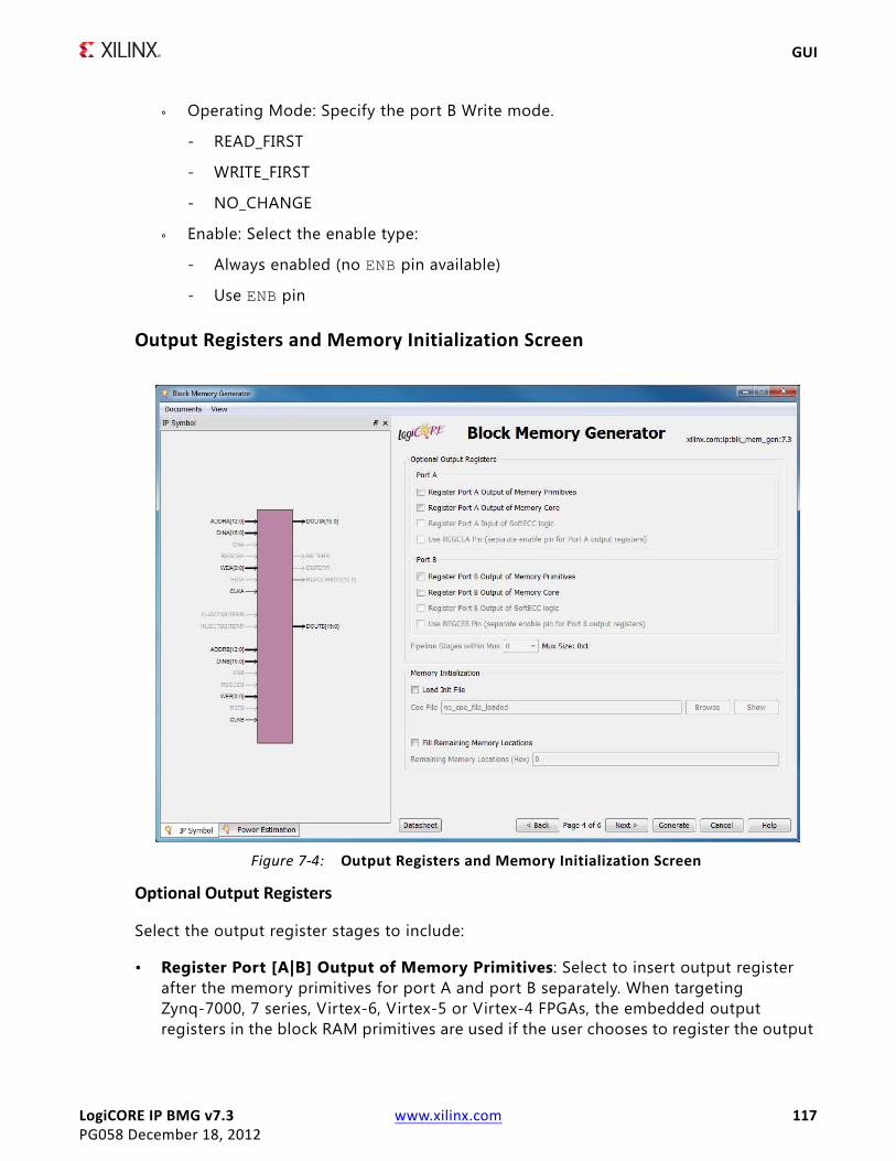
LogiCORE IP BMG v7.3 www.xilinx.com 117PG058 December 18, 2012
GUI
° Operating Mode: Specify the port B Write mode.
- READ_FIRST
- WRITE_FIRST
- NO_CHANGE
° Enable: Select the enable type:
- Always enabled (no ENB pin available)
- Use ENB pin
Output Registers and Memory Initialization Screen
Optional Output Registers
Select the output register stages to include:
• Register Port [A|B] Output of Memory Primitives: Select to insert output register after the memory primitives for port A and port B separately. When targeting Zynq-7000, 7 series, Virtex-6, Virtex-5 or Virtex-4 FPGAs, the embedded output registers in the block RAM primitives are used if the user chooses to register the output
X-Ref Target - Figure 7-4
Figure 7-4: Output Registers and Memory Initialization Screen
LogiCORE IP BMG v7.3 www.xilinx.com 118PG058 December 18, 2012
GUI
of the memory primitives. For Spartan-6 and Spartan-3A DSP, either the primitive embedded registers or fabric registers from FPGA slices are used, depending upon the Reset Behavior option chosen by the user. For other architectures, the registers in the FPGA slices are used. Note that in Virtex-4 devices, the use of the RST input prevents the core from using the embedded output registers. See Output Register Configurations in Appendix D for more information.
• Register Port [A|B] Output of Memory Core: Select for each port (A or B) to insert a register on the output of the memory core for that port. When selected, registers are implemented using FPGA slices to register the core's output.
• Use REGCE [A|B] Pin: Select to use a separate REGCEA or REGCEB input pin to control the enable of the last output register stage in the memory. When unselected, all register stages are enabled by ENA/ENB.
• Pipeline Stages within Mux: Available only when the Register Output of Memory Core option is selected for both port A and port B and when the constructed memory has more than one primitive in depth, so that a MUX is needed at the output. Select a value of 0, 1, 2, or 3 from the drop-down list.
The MUX size displayed in the GUI can be used to determine the number of pipeline stages to use within the MUX. Select the appropriate number of pipeline stages for your design based on the device architecture.
Memory Initialization
Select whether to initialize the memory contents using a COE f ile, and whether to initialize the remaining memory contents with a default value. When using asymmetric port widths or data widths, the COE f ile and the default value are with respect to the port A Write width.

LogiCORE IP BMG v7.3 www.xilinx.com 119PG058 December 18, 2012
GUI
Reset Options Screen
Port [A|B] Output Reset Options
• Use RST[A|B] Pin: Choose whether a set/reset pin (RST[A|B]) is needed.
• Reset Priority: The Reset Priority option for each port is available only when the Use RST Pin option of the corresponding port is chosen. The user can set the reset priority to either CE or SR. For more information on the reset priority feature, see Reset Priority in Chapter 3.
• Reset Behavior : The Reset Behavior (Reset Memory Latch) options for each port are available only when the Use RST Pin option and the Register Output of Memory Primitives option of the corresponding port are chosen, and the Register Memory Core option of the corresponding port is not chosen.
The Reset Memory Latch option modif ies the behavior of the reset and changes the duration for which the reset value is asserted. The minimum duration of reset assertion is displayed as information in the GUI based upon the choice for this option. For more information on the Reset Memory Latch option, see Special Reset Behavior in Chapter 3.
• Output Reset Value (Hex): Specify the reset value of the memory output latch and output registers. These values are with respect to the Read port widths.
X-Ref Target - Figure 7-5
Figure 7-5: Reset Options Screen

LogiCORE IP BMG v7.3 www.xilinx.com 120PG058 December 18, 2012
GUI
Reset Type
The Reset Type option is available only for Spartan-6 devices and when either or both of Use RSTA Pin or Use RSTB Pin option are chosen. The user can set the reset type to either Synchronous or Asynchronous. For more information on this option, see Asynchronous Reset in Chapter 3.
Simulation Model Options and Information ScreenX-Ref Target - Figure 7-6
Figure 7-6: Simulation Model Options and Information Screen

LogiCORE IP BMG v7.3 www.xilinx.com 121PG058 December 18, 2012
GUI
Power Estimate Options Screen
The Power Estimation tab on the left side of the GUI screen shown in Figure 7-7 provides a rough estimate of power consumption for the core based on the configured Read width, Write width, clock rate, Write rate and enable rate of each port. The power consumption calculation assumes a toggle rate 50%. More accurate estimates can be obtained on the routed design using the XPower Analyzer tool. See www.xilinx.com/power for more information on the XPower Analyzer.
The screen has an option to provide "Additional Inputs for Power Estimation" apart from configuration parameters. The following parameters can be entered by the user for power calculation:
• Clock Frequency [A|B]: The operating clock frequency of the two ports A and B respectively.
• Write Rate [A|B]: Write rate of ports A and B respectively.
• Enable Rate [A|B]: Average access rate of port A and B respectively.
X-Ref Target - Figure 7-7
Figure 7-7: Power Estimate Options Screen

LogiCORE IP BMG v7.3 www.xilinx.com 122PG058 December 18, 2012
GUI
Structural/UNISIM Simulation Model Options
Select the type of warning messages and outputs generated by the structural simulation model in the event of collisions. For the options of ALL, WARNING_ONLY and GENERATE_X_ONLY, the collision detection feature will be enabled in the UniSim models to handle collision under any condition.
The NONE selection is intended for designs that have no collisions and clocks (Port A and Port B) that are never in phase or within 3000 ps in skew. If NONE is selected, the collision detection feature will be disabled in the models, and the behavior during collisions is left for the simulator to handle. So, the output will be unpredictable if the clocks are in phase or from the same clock source or within 3000 ps in skew, and the addresses are the same for both ports. The option NONE is intended for design with clocks never in phase.
Behavioral Simulation Model Options
Select the type of warning messages generated by the behavioral simulation model. Select whether the model should assume synchronous clocks (Common Clock) for collision warnings.
Information Section
This section displays an informational summary of the selected core options.
• Memory Type: Reports the selected memory type.
• Block RAM Resources: Reports the exact number of 9K, 18K and 36K block RAM primitives which will be used to construct the core.
• Total Port A Read Latency: The number of clock cycles for a Read operation for port A. This value is controlled by the optional output registers options for port A on the previous screen.
• Total Port B Read Latency: The number of clock cycles for a Read operation for port B. This value is controlled by the optional output registers options for port B on the previous screen.
• Address Width: The actual width of the address bus to each port.
Specifying Initial Memory Contents
The Block Memory Generator core supports memory initialization using a memory coeff icient (COE) file or the default data option in the CORE Generator GUI, or a combination of both.
The COE file can specify the initial contents of each memory location, while default data specifies the contents of all memory locations. When used in tandem, the COE file can specify a portion of the memory space, while default data f ills the rest of the remaining
LogiCORE IP BMG v7.3 www.xilinx.com 123PG058 December 18, 2012
GUI
memory space. COE files and default data is formatted with respect to the port A Write width (or port A Read width for ROMs).
A COE is a text f ile which specif ies two parameters:
• memory_initialization_radix: The radix of the values in the memory_initialization_vector. Valid choices are 2, 10, or 16.
• memory_initialization_vector : Defines the contents of each memory element. Each value is LSB-justif ied, separated by a space, and assumed to be in the radix defined by memory_initialization_radix.
The following is an example COE f ile. Note that semi-colon is the end of line character.
; Sample initialization file for a; 8-bit wide by 16 deep RAMmemory_initialization_radix = 16;memory_initialization_vector = 12, 34, 56, 78, AB, CD, EF, 12, 34, 56, 78, 90, AA, A5, 5A, BA;
Block RAM Usage
The Information panel (screen 5 of the Block Memory Generator GUI) reports the actual number of 9K, 18K and 36K block RAM blocks to be used.
To estimate this value when using the fixed primitive algorithm, the number of block RAM primitives used is equal to the width ratio (rounded up) multiplied by the depth ratio (rounded up), where the width ratio is the width of the memory divided by the width of the selected primitive, and the depth ratio is the depth of the memory divided by the depth of the primitive selected.
To estimate block RAM usage when using the low power algorithm requires a few more calculations:
• If the memory width is an integral multiple of the width of the widest available primitive for the chosen architecture, then the number of primitives used is calculated in the same way as the f ixed primitive algorithm. The width and depth ratios are calculated using the width and depth of the widest primitive. For example, for a memory configuration of 2kx72, the width ratio is 2 and the depth ratio is 4 using the widest primitive of 512x36. As a result, the total available primitives used is 8.
• If the memory width is greater than an integral multiple of the widest primitive, then in addition to the above calculated primitives, more primitives are needed to cover the remaining width. This additional number is obtained by dividing the memory depth by the depth of the additional primitive chosen to cover the remaining width. For example, a memory configuration of 17kx37 requires one 512x36 primitive to cover the width of 36, and an additional 16kx1 primitive to cover the remaining width of 1. To cover the depth of 17K, 34 512x36 primitives and 2 16kx1 primitives are needed. As a result, the total number of primitives used for this configuration is 36.

LogiCORE IP BMG v7.3 www.xilinx.com 124PG058 December 18, 2012
GUI
• If the memory width is less than the width of the widest primitive, then the smallest possible primitive that covers the memory width is chosen for the solution. The total number of primitives used is obtained by dividing the memory depth by the depth of the chosen primitive. For example, for a memory configuration of 2kx32, the chosen primitive is 512x36, and the total number of primitives used is 2k divided by 512, which is 4.
When using the minimum area algorithm, it is not as easy to determine the exact block RAM count. This is because the actual algorithms perform complex manipulations to produce optimal solutions. The optimistic estimate of the number of 18K block RAMs is total memory bits divided by 18k (the total number of bits per primitive) rounded up. Given that this algorithm packs block RAMs very eff iciently, this estimate is often very accurate for most memories.
LUT Utilization and Performance
The LUT utilization and performance of the core are directly related to the arrangement of primitives and the selection of output registers. Particularly, the number of primitives cascaded in depth to implement a memory determines the size of the output multiplexer and the size of the input decoder, which are implemented in the FPGA fabric.
Note: Although the primary goal of the minimum area algorithm is to use the minimum number of block RAM primitives, it has a secondary goal of maximizing performance – as long as block RAM usage does not increase.
Generating the AXI4 Interface Block Memory Generator CoreThe AXI4 Interface Block Memory Generator GUI includes two additional screens followed by Native BMG configuration screens:
• Interface Type Selection Screen
• AXI4 Interface Options
Interface Type Selection Screen
The main Block Memory Generator screen is used to define the component name and provides the Interface Options for the core.
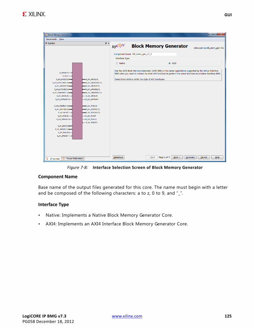
LogiCORE IP BMG v7.3 www.xilinx.com 125PG058 December 18, 2012
GUI
Component Name
Base name of the output f iles generated for this core. The name must begin with a letter and be composed of the following characters: a to z, 0 to 9, and “_”.
Interface Type
• Native: Implements a Native Block Memory Generator Core.
• AXI4: Implements an AXI4 Interface Block Memory Generator Core.
X-Ref Target - Figure 7-8Interface Options for the core.
Figure 7-8: Interface Selection Screen of Block Memory Generator
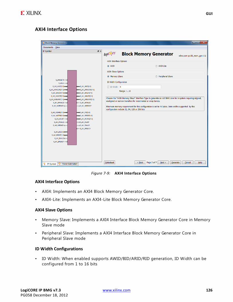
LogiCORE IP BMG v7.3 www.xilinx.com 126PG058 December 18, 2012
GUI
AXI4 Interface Options
AXI4 Interface Options
• AXI4: Implements an AXI4 Block Memory Generator Core.
• AXI4-Lite: Implements an AXI4-Lite Block Memory Generator Core.
AXI4 Slave Options
• Memory Slave: Implements a AXI4 Interface Block Memory Generator Core in Memory Slave mode
• Peripheral Slave: Implements a AXI4 Interface Block Memory Generator Core in Peripheral Slave mode
ID Width Configurations
• ID Width: When enabled supports AWID/BID/ARID/RID generation, ID Width can be configured from 1 to 16 bits
X-Ref Target - Figure 7-9
Figure 7-9: AXI4 Interface Options
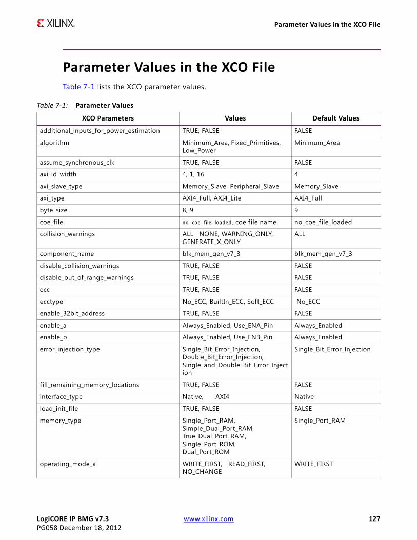
LogiCORE IP BMG v7.3 www.xilinx.com 127PG058 December 18, 2012
Parameter Values in the XCO File
Parameter Values in the XCO FileTable 7-1 lists the XCO parameter values.
Table 7-1: Parameter Values
XCO Parameters Values Default Values
additional_inputs_for_power_estimation TRUE, FALSE FALSE
algorithm Minimum_Area, Fixed_Primitives, Low_Power
Minimum_Area
assume_synchronous_clk TRUE, FALSE FALSE
axi_id_width 4, 1, 16 4
axi_slave_type Memory_Slave, Peripheral_Slave Memory_Slave
axi_type AXI4_Full, AXI4_Lite AXI4_Full
byte_size 8, 9 9
coe_file no_coe_file_loaded, coe f ile name no_coe_file_loaded
collision_warnings ALL NONE, WARNING_ONLY, GENERATE_X_ONLY
ALL
component_name blk_mem_gen_v7_3 blk_mem_gen_v7_3
disable_collision_warnings TRUE, FALSE FALSE
disable_out_of_range_warnings TRUE, FALSE FALSE
ecc TRUE, FALSE FALSE
ecctype No_ECC, BuiltIn_ECC, Soft_ECC No_ECC
enable_32bit_address TRUE, FALSE FALSE
enable_a Always_Enabled, Use_ENA_Pin Always_Enabled
enable_b Always_Enabled, Use_ENB_Pin Always_Enabled
error_injection_type Single_Bit_Error_Injection, Double_Bit_Error_Injection, Single_and_Double_Bit_Error_Injection
Single_Bit_Error_Injection
fill_remaining_memory_locations TRUE, FALSE FALSE
interface_type Native, AXI4 Native
load_init_file TRUE, FALSE FALSE
memory_type Single_Port_RAM, Simple_Dual_Port_RAM, True_Dual_Port_RAM, Single_Port_ROM, Dual_Port_ROM
Single_Port_RAM
operating_mode_a WRITE_FIRST, READ_FIRST, NO_CHANGE
WRITE_FIRST

LogiCORE IP BMG v7.3 www.xilinx.com 128PG058 December 18, 2012
Parameter Values in the XCO File
operating_mode_b WRITE_FIRST, READ_FIRST, NO_CHANGE
WRITE_FIRST
output_reset_value_a Any binay, decimal and hexadecimal values equal to the data width
0
output_reset_value_b Any binay, decimal and hexadecimal values equal to the data width
0
pipeline_stages 0, 1, 2, 3 0
port_a_clock 0 - 800 100
port_a_enable_rate 0 - 100 100
port_a_write_rate 0 - 100 50
port_b_clock 0 - 800 100
port_b_enable_rate 0 - 100 100
port_b_write_rate 0 - 100 50
primitive 32kx1, 16kx1, 8kx2, 4kx4, 2kx9, 1kx18, 512x36, 256x72, 256x36
8kx2
read_width_a 1, 2, 4, 8, 16, 32 16
read_width_b 1, 2, 4, 8, 16, 32 16
register_porta_input_of_softecc TRUE, FALSE FALSE
register_porta_output_of_memory_core TRUE, FALSE FALSE
register_porta_output_of_memory_primitives TRUE, FALSE FALSE
register_portb_output_of_memory_core TRUE, FALSE FALSE
register_portb_output_of_memory_primitives TRUE, FALSE FALSE
register_portb_output_of_softecc TRUE, FALSE FALSE
remaining_memory_locations Any binay, decimal and hexadecimal values equal to the data width
0
reset_memory_latch_a TRUE, FALSE FALSE
reset_memory_latch_b TRUE, FALSE FALSE
reset_priority_a CE, SR CE
reset_priority_b CE, SR CE
reset_type SYNC, ASYNC SYNC
softecc TRUE, FALSE FALSE
use_axi_id TRUE, FALSE FALSE
use_byte_write_enable TRUE, FALSE FALSE
use_error_injection_pins TRUE, FALSE FALSE
Table 7-1: Parameter Values (Cont’d)
XCO Parameters Values Default Values

LogiCORE IP BMG v7.3 www.xilinx.com 129PG058 December 18, 2012
Output Generation
Output GenerationThe top-level project directory, <project_directory>, for the CORE Generator software contains the following directories:
<project_directory>/<component_name>
Contains the Block Memory Generator release notes text f ile.
<component_name>/example designVerilog and VHDL design f iles.
<component_name>/implementImplementation script f iles.
<component_name>/implement/resultsCreated after implementation scripts are run and contains implement script results.
<component_name>/simulationContains the test bench and other supporting source f iles used to create the Block Memory Generator simulation model.
<component_name>/simulationContains the test bench and other supporting source f iles used to create the Block Memory Generator simulation model.
simulation/functionalFunctional simulation scripts.
simulation/timingTiming simulation scripts.
Directory and File ContentsThis section contains details about the directories of the example design.
use_regcea_pin TRUE, FALSE FALSE
use_regceb_pin TRUE, FALSE FALSE
use_rsta_pin TRUE, FALSE FALSE
use_rstb_pin TRUE, FALSE FALSE
write_depth_a 2 - 9011200 16
write_width_a 1 - 4096 16
write_width_b 1 - 4096 16
Table 7-1: Parameter Values (Cont’d)
XCO Parameters Values Default Values

LogiCORE IP BMG v7.3 www.xilinx.com 130PG058 December 18, 2012
Output Generation
<project_directory>
The <project_directory> contains all the CORE Generator software project f iles.
<project_directory>/<component_name>
The <component_name> directory contains the release notes text f ile included with the core that contains last-minute changes and or updates.
<component_name>/example design
The example design directory contains the example design f iles provided with the core.
Table 7-2: Project Directory
Name Description
<project_directory>
<component_name>.ngc Top-level netlist.
<component_name>.v[hd] Verilog or VHDL simulation model .
<component_name>.xco CORE Generator software project-specific option file; can be used as an input to the CORE Generator software.
<component_name>_flist.txt List of f iles delivered with the core.
<component_name>.{veo|vho} VHDL or Verilog instantiation template.
Back To Top
Table 7-3: Component Name Directory
Name Description
<project_directory>/<component_name>
blk_mem_gen_v7_3_readme.txt Core name release notes f ile.
Back To Top
Table 7-4: Example Design Directory
Name Description
<project_directory>/<component_name>/example_design
<component_name>_top.ucf Provides example constraints necessary for processing the Block Memory Generator core using the Xilinx implementation tools.
<component_name>_exdes.vhd The VHDL top-level f ile for the example design; it instantiates the Block Memory Generator core. This f ile contains entity with the IO's required for the core configuration.

LogiCORE IP BMG v7.3 www.xilinx.com 131PG058 December 18, 2012
Output Generation
<component_name>/implement
The implement directory contains the core implementation script f iles.
<component_name>/implement/results
The results directory is created by the implement script, after which the implement script results are placed in the results directory.
<component_name>/simulation
The simulation directory contains the demo test bench f iles provided with the core.
<component_name>_top_wrapper.v[hd] The VHDL wrapper file for the example design <component_name>_top.vhd f ile. This f ile contains entity with all ports of Block Memory Generator core.
Back To Top
Table 7-5: Implement Directory
Name Description
<project_directory>/<component_name>/implement
implement.{bat|sh} A Windows (.bat) or Linux script that processes the example design.
xst.prj The XST project f ile for the example design that lists all of the source files to be synthesized. Only available when the CORE Generator software project option is set to ISE or Other.
xst.scr The XST script f ile for the example design used to synthesize the core. Only available when the CORE Generator software Vendor project option is set to ISE or Other.
Back To Top
Table 7-6: Results Directory
Name Description
<project_directory>/<component_name>/results
Implement script result f iles.
Back To Top
Table 7-4: Example Design Directory (Cont’d)
Name Description
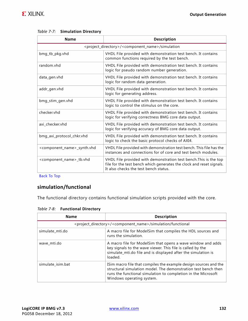
LogiCORE IP BMG v7.3 www.xilinx.com 132PG058 December 18, 2012
Output Generation
simulation/functional
The functional directory contains functional simulation scripts provided with the core.
Table 7-7: Simulation Directory
Name Description
<project_directory>/<component_name>/simulation
bmg_tb_pkg.vhd VHDL File provided with demonstration test bench. It contains common functions required by the test bench.
random.vhd VHDL File provided with demonstration test bench. It contains logic for pseudo random number generation.
data_gen.vhd VHDL File provided with demonstration test bench. It contains logic for random data generation.
addr_gen.vhd VHDL File provided with demonstration test bench. It contains logic for generating address.
bmg_stim_gen.vhd VHDL File provided with demonstration test bench. It contains logic to control the stimulus on the core.
checker.vhd VHDL File provided with demonstration test bench. It contains logic for verifying correctness BMG core data output.
axi_checker.vhd VHDL File provided with demonstration test bench. It contains logic for verifying accuracy of BMG core data output.
bmg_axi_protocol_chkr.vhd VHDL File provided with demonstration test bench. It contains logic to check the basic protocol checks of AXI4.
<component_name>_synth.vhd VHDL File provided with demonstration test bench. This f ile has the instances and connections for of core and test bench modules.
<component_name>_tb.vhd VHDL File provided with demonstration test bench.This is the top f ile for the test bench which generates the clock and reset signals. It also checks the test bench status.
Back To Top
Table 7-8: Functional Directory
Name Description
<project_directory>/<component_name>/simulation/functional
simulate_mti.do A macro f ile for ModelSim that compiles the HDL sources and runs the simulation.
wave_mti.do A macro f ile for ModelSim that opens a wave window and adds key signals to the wave viewer. This f ile is called by the simulate_mti.do f ile and is displayed after the simulation is loaded.
simulate_isim.bat ISim macro f ile that compiles the example design sources and the structural simulation model. The demonstration test bench then runs the functional simulation to completion in the Microsoft Windows operating system.

LogiCORE IP BMG v7.3 www.xilinx.com 133PG058 December 18, 2012
Output Generation
simulation/timing
The timing directory contains functional simulation scripts provided with the core.
simulate_isim.sh ISim macro f ile that compiles the example design sources and the structural simulation model. The demonstration test bench then runs the functional simulation to completion in the Linux operating system.
simcmds.tcl ISim macro f ile that opens a Wave window with top-level signals.
simulate_ncsim.sh Linux shell script that compiles the example design sources and the structural simulation model then runs the functional simulation to completion using the Cadence IES simulator.
wave_ncsim.sv The Cadence IES simulator macro f ile that opens a wave window and adds interesting signals to it. This macro is called by the simulate_ncsim.sh script.
Back To Top
Table 7-9: Timing Directory
Name Description
<project_directory>/<component_name>/simulation/timing
simulate_mti.do A macro f ile for ModelSim that compiles the HDL sources and runs the simulation.
wave_mti.do A macro f ile for ModelSim that opens a wave window and adds key signals to the wave viewer. This f ile is called by the simulate_mti.do f ile and is displayed after the simulation is loaded.
simulate_isim.bat ISim macro f ile that compiles the example design sources and the structural simulation model. The demonstration test bench then runs the functional simulation to completion in the Microsoft Windows operating system.
simulate_isim.sh ISim macro f ile that compiles the example design sources and the structural simulation model. The demonstration test bench then runs the functional simulation to completion in the Linux operating system.
simcmds.tcl ISim macro f ile that opens a Wave window with top-level signals.
Table 7-8: Functional Directory (Cont’d)
Name Description
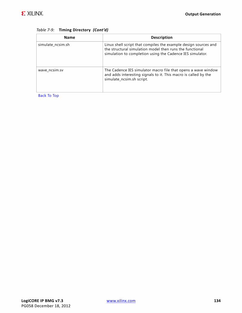
LogiCORE IP BMG v7.3 www.xilinx.com 134PG058 December 18, 2012
Output Generation
simulate_ncsim.sh Linux shell script that compiles the example design sources and the structural simulation model then runs the functional simulation to completion using the Cadence IES simulator.
wave_ncsim.sv The Cadence IES simulator macro f ile that opens a wave window and adds interesting signals to it. This macro is called by the simulate_ncsim.sh script.
Back To Top
Table 7-9: Timing Directory (Cont’d)
Name Description

LogiCORE IP BMG v7.3 www.xilinx.com 135PG058 December 18, 2012
Chapter 8
Constraining the Core
Required ConstraintsThe Block Memory Generator core provides a sample clock constraint. This sample constraint can be added to the user's design constraint f ile.
Device, Package, and Speed Grade SelectionsSee IP Facts for details about support devices.
Clock FrequenciesThere are no additional clock frequency constraints for this core.
Clock ManagementThere are no additional clock management constraints for this core.
Clock PlacementThere are no additional clock placement constraints for this core.
BankingThere are no banking constraints for this core.

LogiCORE IP BMG v7.3 www.xilinx.com 136PG058 December 18, 2012
Transceiver Placement
Transceiver PlacementThere are no transceiver constraints for this core.
I/O Standard and PlacementThere are no I/O constraints for this core.

LogiCORE IP BMG v7.3 www.xilinx.com 137PG058 December 18, 2012
Chapter 9
Detailed Example DesignThis chapter provides details on the example design included with the core.
Directory and File ContentsSee Output Generation in Chapter 7 for a detailed list of f iles generated with the example design.
Example DesignFigure 9-1 shows the configuration of the example design.
The example design contains the following:
• An instance of the Block Memory Generator core. During simulation, the Block Memory Generator core is instantiated as a black box and replaced with the CORE Generator software netlist model during implementation for timing simulation or XST netlist/behavioral model for the functional simulation.
• Global clock buffers for top-level port clock signals.
Demonstration Test BenchFigure 9-2 shows a block diagram of the demonstration test bench.
X-Ref Target - Figure 9-1
Figure 9-1: Example Design Configuration

LogiCORE IP BMG v7.3 www.xilinx.com 138PG058 December 18, 2012
Demonstration Test Bench
Test Bench Functionality
The demonstration test bench is a straightforward VHDL f ile to exercise the example design and the core itself. The test bench consists of the following:
• Clock Generators
• Address and data generator module
• Stimulus generator module
• Data checker
• Protocol checks for the AXI4 protocol
Core with Native Interface
The demonstration test bench in a core with a Native interface performs the following tasks:
• Input clock signals are generated.
• A reset is applied to the example design. Address is generated in a linear incremented format.
• Pseudo random data is generated and given as input to BMG data input port.
• During Reads, data out is compared with another pseudo-random generator with the same seed used for input data random generator.
• Core is exercised with 256 write and read transactions
X-Ref Target - Figure 9-2
Figure 9-2: Demonstration Test Bench

LogiCORE IP BMG v7.3 www.xilinx.com 139PG058 December 18, 2012
Implementation
Core with AXI4 Interface
The demonstration test bench in a core with an AXI4 interface performs the following tasks:
• Input clock signals are generated.
• A reset is applied to the example design.
• Stimulus is generated only when incremented burst and narrow transactions are not exercised.
• Address is generated in a linear incremented format.
• Pseudo-random data is generated for WDATA.
• Length (AWLEN/ARLEN) is determined randomly.
• During read, RDATA is compared with another pseudo-random generator with the same seed as WDATA random data generator.
• A basic AXI4 protocol checker checks the protocol violations.
• Core is exercised with 256 AXI4 write and read transactions.
ImplementationThe implementation script is either a shell script (.sh) or batch f ile (.bat) that processes the example design through the Xilinx tool flow. It is located at:
Linux
<project_dir>/<component_name>/implement/implement.sh
Windows
<project_dir>/<component_name>/implement/implement.bat
The implement script performs these steps:
• Synthesizes the HDL example design f iles using XST
• Runs NGDBuild to consolidate the core netlist and the example design netlist into the NGD file containing the entire design
• Maps the design to the target technology
• Place-and-routes the design on the target device
• Performs static timing analysis on the routed design using Timing Analyzer (TRCE)
• Generates a bitstream

LogiCORE IP BMG v7.3 www.xilinx.com 140PG058 December 18, 2012
Simulation
• Enables Netgen to run on the routed design to generate a VHDL or Verilog netlist (as appropriate for the Design Entry project setting) and timing information in the form of SDF f iles
The Xilinx tool flow generates several output and report f iles. These are saved in the following directory which is created by the implement script:
<project_dir>/<component_name>/implement/results
SimulationThis section contains details about the test scripts included in the example design.
Functional Simulation
The test scripts are ModelSim macros that automate the simulation of the test bench. They are available from the following location:
<project_dir>/<component_name>/simulation/functional/
The test script performs these tasks:
• Compiles the behavioral model/structural UNISIM simulation model
• Compiles HDL Example Design source code
• Compiles the demonstration test bench
• Starts a simulation of the test bench
• Opens a Wave window and adds signals of interest (wave_mti.do)
• Runs the simulation to completion
Timing Simulation
The test scripts are ModelSim macros that automate the simulation of the test bench. They are located in:
<project_dir>/<component_name>/simulation/timing/
The test script performs these tasks:
• Compiles the SIMPRIM based gate level netlist simulation model
• Compiles the demonstration test bench
• Starts a simulation of the test bench
• Opens a Wave window and adds signals of interest (wave_mti.do)

LogiCORE IP BMG v7.3 www.xilinx.com 141PG058 December 18, 2012
Messages and Warnings
• Runs the simulation to completion
Messages and WarningsWhen the functional or timing simulation has completed successfully, the test bench displays the following message, and it is safe to ignore this message.
Failure: Test Completed Successfully

LogiCORE IP BMG v7.3 www.xilinx.com 142PG058 December 18, 2012
SECTION IV: APPENDICES
Verification, Compliance, and Interoperability
Migrating
Debugging
Native Block Memory Generator Supplemental Information
Additional Resources

LogiCORE IP BMG v7.3 www.xilinx.com 143PG058 December 18, 2012
Appendix A
Verification, Compliance, and Interoperability
The Block Memory Generator core and the simulation models delivered with it are rigorously verif ied using advanced verif ication techniques, including a constrained random configuration generator and a cycle-accurate bus functional model.
SimulationThe Block Memory Generator has been tested with Xilinx ISE® Design Suitev14.4, Xilinx Vivado Design Suite v2012.4, Xilinx ISIM/XSIM, Cadence Incisive Enterprise Simulator (IES), Synopsys VCS and VCS MX and Mentor Graphics ModelSim simulator.

LogiCORE IP BMG v7.3 www.xilinx.com 144PG058 December 18, 2012
Appendix B
MigratingThis appendix provides step-by-step instructions for migrating designs containing instances of either the legacy memory cores (Dual Port Block Memory and Single Port Block Memory cores) or older versions of the LogiCORE™ IP Block Memory Generator core to the latest version of the Block Memory Generator core.
TIP: For new designs, Xilinx recommends that you use the most recent version of the Block Memory Generator core for all block memory function requirements.
For information on migrating to the Vivado™ Design Suite, see UG911, Vivado Design Suite Migration Methodology Guide.
Migration OverviewTwo types of core migration are available: manual and automated. Manual migration includes converting the XCO file(s) of the legacy cores or the XCO file(s) of the older Block Memory Generator cores to XCO file(s) of the latest version of the Block Memory Generator core, generating a new core, and modifying the instantiations of the new cores. Automated migration, provided in the Block Memory Generator Migration Kit, uses a Perl script to automate the migration process.
A prerequisite for using the Migration Kit is that the device family of the user’s old Block Memory design should be supported by the latest version of the Block Memory Generator core. Designs using unsupported families will have to be re-targeted to one of the supported device families. For information on the supported device families, see IP Facts, page 6.
Before starting the migration process, do the following:
• Evaluate the differences between the core features, page 145
• Determine which migration process to use:
° Automated Migration, page 149
° Manual Migration, page 155

LogiCORE IP BMG v7.3 www.xilinx.com 145PG058 December 18, 2012
Differences Between Cores
Differences Between CoresThe Block Memory Generator core leverages the capabilities of Xilinx FPGA embedded block RAM primitives to automatically build a wide range of single and dual port memories by concatenating Xilinx FPGA block RAM primitives in an optimal manner. Use of an enhanced algorithm optimizes block RAM primitive resource utilization and creates a higher level of performance than previous generations of block memory cores.
Core Compatibility
Core Compatibility with Legacy Block Memory Cores
The Block Memory Generator core is not backward compatible with the Single and Dual Port Block Memory cores in the following ways:
• Pin polarity, handshaking, and input register features supported by the previous generation memory cores are not supported in the Block Memory Generator.
• The behavior of synchronous set/reset pin (RST) in the Block Memory Generator differs from the previous generation v6.x cores when using optional output registers.
• The Single Port Block Memory v6.x core and the Block Memory Generator do not have the same port names for a single-port memory configuration.
• The Dual Port Block Memory core and the Block Memory Generator do not have the same reset port name.
• The XCO files for the previous generation memory cores are not compatible with the Block Memory Generator.
• Not all combinations of Read and Write, Write Only, and Read Only port configurations are natively supported by Dual Port memories generated in the new Block Memory Generator. In these cases, generate a True Dual Port RAM and manually tie-off the unused port (automated if using the Migration Kit).
Differences in port names and XCO parameters are provided in “Convert the XCO File” on page 156 and “Modifying Instantiations of the Old Core” on page 163.
Core Compatibility with Older versions of Block Memory Generator Core
Versions of the Block Memory Generator core newer than 2.x are not backward compatible with the 1.x and 2.x versions of the Block Memory Generator cores in the following ways:
• The names of the reset ports have been changed.
• The names of some of the reset related XCO parameters have changed.

LogiCORE IP BMG v7.3 www.xilinx.com 146PG058 December 18, 2012
Differences Between Cores
• The XCO files of the previous versions of the Block Memory Generator core are not compatible with version 7.3 of the Block Memory Generator core.
Differences in port names and XCO parameters are provided in “Convert the XCO File” on page 156 and “Modifying Instantiations of the Old Core” on page 163.
Obsolete Features of Legacy Block Memory Cores
Pin Polarity Option
The Block Memory Generator does not support pin polarity options on the clock, enable, write enable, and set/reset input pins. When active low signaling is desired, users can invert the signals prior to the input of the core. Where possible, the inversion is automatically absorbed into the memory primitives when the design is processed by the ISE® Mapper.
Handshaking Pins
The Block Memory Generator does not support handshaking pins: ND[A|B], RFD[A|B], and RDY[A|B]. Figure B-1 illustrates how to implement this logic in a design.
Input Registers
The Block Memory Generator does not support input registers on ports DIN, ADDR, and WE prior to accessing the memory primitives. To implement this feature, add one stage of pipeline registers to the input of the Block Memory Generator core.
X-Ref Target - Figure B-1
Figure B-1: Handshaking Pin Design
EN
RFD
Input Reg Output Pipeline
ND
SINIT
CLK
Enable PinPolarity
D Q Q Q
CE
D
CE
D
CE
RST RST RST
Optional Handshaking Signals

LogiCORE IP BMG v7.3 www.xilinx.com 147PG058 December 18, 2012
Differences Between Cores
Port Configuration/Memory Type
Not all combinations of Read and Write, Write Only, and Read Only port configurations are natively supported by Dual Port memories generated in the new Block Memory Generator. Table B-1 defines the relationship between Dual Port Block Memory v6.x configurations and the equivalent implementation using the Block Memory Generator. The Migration Kit automatically maps Dual Port Block Memory v6.x instantiations to the equivalent Block Memory Generator usage, including tying-off the unused ports.
Modified Behaviors of Legacy Block Memory Cores
Enable Pin
The Block Memory Generator provides two enable pin options:
• REGCE pin only controls the enables of the registers in the last output stage.
• EN pin controls the enables of all other registers and memory, and in the absence of a REGCE pin, also controls the enables of the registers in the last output stage.
The v6.x memory cores only provide a core-wide enable (second option).
Synchronous Reset Pin
In the Block Memory v6.x cores, the synchronous reset (SINIT pin) initializes all memory latches and output registers. With the Block Memory Generator core, the synchronous set/reset (RST pin) only resets the registers in the last output stage. When there are no output register stages present, it initializes the memory latches.
Table B-1: Block Memory Generator Port Configurations with Memory Types
Dual Port Block Memory Core Block Memory Generator Core
Port A Configuration Port B Configuration Memory Type Notes
Read and Write Read and Write True Dual Port RAM N/A
Write Only Read Only Simple Dual Port RAM N/A
Read Only Read Only Dual Port RAM N/A
Read Only Read and Write True Dual Port RAM Tie-off Write Port A
Write Only Read and Write True Dual Port RAM Tie-off Read Port A
Read and Write Read Only True Dual Port RAM Tie-off Write Port B
Read and Write Write Only True Dual Port RAM Tie-off Read Port B
Read Only Write Only Simple Dual Port RAM Reverse A and B Ports

LogiCORE IP BMG v7.3 www.xilinx.com 148PG058 December 18, 2012
Differences Between Cores
Output Registers
The Block Memory v6.x cores allowed you to add an additional output pipeline register stage on the output of the block RAM. With the Block Memory Generator, you have better control on where and how these output registers are implemented. Output registers can be added to the following locations:
• Output of the block RAM primitives (before output multiplexing)
• Output of the core (after output multiplexing)
• Pipeline register stages within the MUX
When targeting the Virtex®-4 FPGA architecture, the primitive output register stage is implemented using the embedded register in Virtex-4 FPGA block RAM when the RST pin is not used. For all other Virtex-4 FPGA configurations and their derivatives, all output register stages are implemented in the FPGA fabric.
The Block Memory Generator core provides optional pipeline stages within the MUX, available only when the registers at the output of the memory core are enabled and only for specific configurations. For the available configurations, the number of pipeline stages can be 1, 2, or 3.
Changes in WEA/WEB Signal Type (VHDL)
In the Block Memory Generator core, the width of the write enable input signals (WEA , WEB) can vary depending on the configuration. The width of the write enable buses are larger than 1 bit only if the byte write enable feature is used. To accommodate this, the write enable signal is always a bus of type std_logic_vector instead of std_logic in VHDL, even when the width of the signal is 1 bit.
When migrating from the Single Port Block Memory or Dual Port Block Memory cores to the Block Memory Generator, be aware that the WEA/WEB inputs in the Block Memory Single Port and Dual Port cores are of type std_logic, whereas the WEA/WEB inputs of the Block Memory Generator are of type std_logic_vector. When the write enable is only 1-bit wide, this change requires the use of a different method to connect the WEA/WEB inputs to the rest of the design.
To connect the WEA port:
1. Declare an intermediate signal of type std_logic_vector for the write enable. This is the signal that connects to the Block Memory Generator WEA port in the instantiation.
Example:
signal we_int: std_logic_vector(0 downto 0);
2. Assign your write enable input (of type std_logic) to bit 0 of the 1-bit-wide intermediate signal.

LogiCORE IP BMG v7.3 www.xilinx.com 149PG058 December 18, 2012
Using the Migration Kit
Example:
signal <user_wea>: std_logic;
we_int(0) <= <user_wea>;
3. Connect the intermediate signal you created and assigned during your instantiation of the Block Memory Generator to the WEA port of the core.
Example:
user_bmg: bmg_inst PORT MAP (
WEA => we_int;
...other port connections...
);
Note: This change in WEA/WEB type does not affect customers using Verilog.
A full example instantiation of the Block Memory Generator core is shown below:
signal we_int: std_logic_vector(0 downto 0);
signal <user_wea>: std_logic;
...
we_int(0) <= <user_wea>;
...
--Instantiate the new BMG core
uut: blk_mem_gen_v3_1
port map (
dina => <user_dina>,
wea => we_int,
addra => <user_addra>,
rsta => <user_rsta>,
douta => <user_douta>,
clka => <user_clka>,
ena => <user_ena>
);
Using the Migration KitThe Migration Kit provides two Perl scripts to help automate the process of converting existing v6.x Legacy Block Memory cores or older versions of the Block Memory Generator core to the latest version of the Block Memory Generator core.
• The primary migration script automates all the manual steps, from converting the XCO file to modifying the instantiation of the old core. In addition, this script can be used to

LogiCORE IP BMG v7.3 www.xilinx.com 150PG058 December 18, 2012
Using the Migration Kit
select only specif ic steps to automate, making it useful as part of the manual migration process.
• The second script recreates XCO files from EDIF or NGC netlists, if necessary (see Script Limitations for more information).
Primary Migration Script
If you can provide all the original design f iles, the primary migration script (bmg_migrate.pl) completely and seamlessly automates the migration process by executing the following steps:
1. Converts old XCO files to new XCO files
2. Modifies instantiations of old cores to new cores including changing port names
3. Adds logic to implement obsolete features (input registers, signal polarity, enable, and reset behaviors)
4. Generates new netlists by calling the CORE Generator™ software Graphical User Interface (GUI) with the new XCO and related COE files
5. Restores original design files, if necessary
Recover XCO Script
If you do not have the v6.x XCO files and/or the related COE f iles, the recover XCO script (recover_xco.pl) can recreate the old v6.x XCO files from your netlist(s).
This script performs the following steps:
1. Scans the netlist(s) to determine the required values for the parameters in the XCO file.
2. Generates COE f ile(s) (initialization f ile) if initial values for the block RAMs have been specified in the netlist.
Supported Platforms
• Windows® 2000
• Windows XP Pro
• Red Hat® Enterprise WS
About the Migration ScriptThe migration script, bmg_migrate.pl, can operate on various inputs and create a variety of outputs based on user-specified command line options.

LogiCORE IP BMG v7.3 www.xilinx.com 151PG058 December 18, 2012
Using the Migration Kit
When using the script as part of the standard, fully-automated flow, you supply the script with one or more of these three f ile types:
• Single Port and/or Dual Port Block Memory XCO core configuration f iles or XCO configuration f iles of the older versions of the Block Memory Generator core (created by the GUI when these cores were generated)
• HDL source f ile(s) containing the core instantiations (VHDL or Verilog)
• COE files used to initialize the memory (if necessary)
The path to the COE file is defined in the XCO file. If you do not have the COE file available, use the recover_xco.pl script to recover it (see Script Limitations, page 153). The recover_xco.pl script can also be used to regenerate the original v6.x XCO file if it is not available.
From the script options, choose one or more of the following migration steps. All selected steps are automatically performed by the script.
• Convert XCO files of the Legacy Block Memory cores or the older versions of the Block Memory Generator core to Block Memory Generator XCO files of the latest version.
• Convert the instantiations of the old cores in your HDL source code to instances of the latest version of the Block Memory Generator core.
• Add logic to implement obsoleted features to make the new core backward compatible with the legacy instances.
• Generate the new netlists by running the CORE Generator software.
The script modif ies and overwrites all input f iles so that the external project f iles and scripts do not need to be updated with new file names or locations. Although the script also automatically generates a backup of all f iles it modifies, it is strongly recommended that you create a backup of all project f iles before running the migration script.
Output Products
Depending on the chosen command line option, the script overwrites the input XCO files, modif ies the input HDL f iles, and optionally generates Block Memory Generator netlists (in the same location as the XCO files).
The script creates a ./bmg_migrate_bak_<xcofilename> backup directory for each XCO file in which a copy of all f iles modified by the migration process is placed. It also generates a restore script in this directory, restore_files.pl, to allow you to restore the original f iles if necessary.
Supported Features for Legacy Block Memory Cores
The migration script adds code to your HDL source f iles to supplement features that have become obsolete in the Block Memory Generator core, making your design almost drop-in

LogiCORE IP BMG v7.3 www.xilinx.com 152PG058 December 18, 2012
Using the Migration Kit
compatible with the original design containing the v6.x memory cores (see Script Limitations, page 153 for details).
The script can add the following features to the Block Memory Generator core:
• Support for inverted clock and enable signals
• Support for input registers
• Support for handshaking signals
Using the Migration Script
To start the Migration Script, type the commands specif ic to your environment at the command prompt.
Note: The ISE 12.3 software requires a CGP file when CORE Generator is run in a command line. To help the user, the Migration Script comes with a sample CGP file (coregen.cgp). The user can modify the sample CGP file according to the user's requirement. THe modified CGP file should be kept in the user directory where the XCO file and instantiation f iles are located. The CGP file name must be coregen.cgp.
Linux
<path to script>/bmg_migrate.pl [-x [-n]] [-m <HDL file(s)>] <xco file>
Windows
xilperl <path to script>\bmg_migrate.pl [-x [-n]]-m <HDL file(s)>] <xco file>
You must use at least one of the following options in the command string:
• -x. Creates an XCO output files needed by the CORE Generator software to generate the core. Requires an input of the old XCO file.
• -n. Calls the CORE Generator software to generate Block Memory Generator netlists necessary to synthesize the design. This option must be used in tandem with the -x option.
• -m. Modif ies the HDL source f iles containing the core instantiations, converting the old instantiations and adding compatibility code where needed. Requires at least one old XCO file and one HDL design file containing old core instantiations.
<HDL file(s)> is a list of one or more HDL f iles containing instantiations of the cores described by the XCO files. These files can be referenced from directories other than the working directory. The HDL f iles listed with an XCO file must have instances with the same configuration as described by the XCO file.
<xco file> is a core configuration f ile of either the Legacy v6.x Block Memory cores or older versions of the Block Memory Generator core, which is to be converted to

LogiCORE IP BMG v7.3 www.xilinx.com 153PG058 December 18, 2012
Using the Migration Kit
configuration file of the latest version of the Block Memory Generator core. This f ile can be referenced from directories other than the working directory.
To reverse the changes made by the script, go to the backup directory of the XCO file at ./bmg_migrate_bak_<xcofilename> and then run xilperl script restore_files.pl.
Usage Examples
bmg_migrate.pl -x -m -n my_design.v my_old_core.xco
1. Creates a Block Memory Generator version of my_old_core.xco.
2. Modif ies the instantiations of my_old_core in my_design.v.
3. Runs CORE Generator software to generate the Block Memory Generator version of my_old_core.ngc netlist f ile.
bmg_migrate.pl -x my_mem_core.xco
1. Creates a Block Memory Generator version of my_mem_core.xco.
If an invalid Block Memory Generator version is given in the XCO, the script prompts the user to input a valid Block Memory Generator version.
Script Limitations
Block Memory Generator cores generated using the migration tool are backward compatible with the legacy v6.x Block Memory cores and the older versions of the Block Memory Generator.
The migration script can successfully read and parse most HDL f iles. Files written using standard coding styles and following standard Xilinx design methodologies (for example, using the CORE Generator software HDL instantiation templates typically generated with the cores) are handled appropriately. If the script cannot properly read and parse the user input HDL f iles, you must perform the conversion manually (see Migrating a Design Manually).
Recover XCO ScriptThe recover_xco.pl script scans netlists containing legacy v6.x Block Memory cores or older versions of the Block Memory Generator core and regenerates XCO and COE files of the respective core from them. It can be used to recover XCO or COE files from a design netlist if either of these types of f iles is missing. COE f iles are recovered only if there is memory initialization data within the netlist; this occurs by simulating the core using the Xilinx ISIM simulator. After recovering the XCO and/or COE files, run the migration script to create the new Block Memory Generator counterparts.
Using the Recover XCO Script
Note: To run this script, ISIM must be installed as part of ISE.
LogiCORE IP BMG v7.3 www.xilinx.com 154PG058 December 18, 2012
Using the Migration Kit
To start the Recover XCO script, type the commands specif ic to your environment at the command prompt. The Recover XCO script requires an input CORE Generator software project f ile (*.CGP).
Linux
<path to script>/recover_xco.pl -cgp=<coregen_project_file.cgp> <netlist(s)>
Windows
xilperl <path to script>\recover_xco.pl -cgp=<coregen_project_file.cgp> <netlist(s)>
For All Platforms
• <netlist(s)> is a list of netlist f iles of v6.x Block Memory core or old Block Memory Generator core versions in EDN or NGC format.
• <coregen_project_file.cgp> is a software project f ile (*.CGP) containing the project options to be applied to the output XCO file. If a CGP f ile is not available, you can create one by creating a new project in GUI. When creating the new project, you will be prompted to set project parameters such as target device, family, HDL language format (VHDL or Verilog), implementation output format, etc.
Note: You do not need to regenerate the v6.x core after recreating the CORE Generator software project f ile.
The script automatically detects if the block RAMs were initialized and runs ISIM simulation to extract initial values in the memory into a COE f ile.
Usage Examples
recover_xco.pl -cgp=coregen.cgp my_old_core.edn dp_mem.ngc
1. Scans the netlists and generates my_old_core.xco and dp_mem.xco f iles.
2. May create COE f iles if initialization data is embedded in the input netlist f ile.
recover_xco.pl -cgp=../proj/my_coregen.cgp ../netlists/my_rom.edn
Scans the netlists and generates ../netlists/my_rom.xco and ../netlists/my_rom.coe.
Using the Perl Scripts with a Windows OSWhen running the Perl scripts in the Windows environment, the scripts must be invoked using a Perl program such as xilperl, which is distributed with Xilinx ISE software. The scripts are intended to be executed within a Windows command window (DOS shell).

LogiCORE IP BMG v7.3 www.xilinx.com 155PG058 December 18, 2012
Migrating a Design Manually
Example Windows Usage
The location of HDL f iles and CORE Generator software netlists may differ from project to project. Assume that project HDL files are stored in c:\xilinx\my_proj\hdl, and Block Memory netlists and XCO files are in c:\xilinx\my_proj\ip_cores. Copy the migration scripts (bmg_migrate.pl and recover_xco.pl) into the c:\xilinx\my_proj directory.
Open a command window:
1. From the Windows Start menu, choose Run; then type cmd in the Run dialog box.
2. At the command prompt, type the following:
C:\> cd \xilinx\my_proj
C:\xilinx\my_proj> xilperl bmg_migrate.pl -v7.3 -x -n -m hdl\top.v ip_cores\dp_ram.xco
The script performs the XCO conversion, modifies the HDL files containing the core instantiations, and generates new Block Memory Generator netlists. A new file, bmg_migrate.log is created, as well as a new subdirectory, c:\xilinx\my_proj\bmg_migrate_bak containing backups of all modif ied f iles.
Invoking the Restore_files Script
To invoke the restore_files.pl script, enter the following at the command prompt:
C:\> cd \xilinx\my_proj\bmg_migrate_bak
C:\xilinx\my_proj\bmg_migrate_bak> xilperl restore_files.pl
This effectively reverses the migration process by restoring any f iles modif ied by the bmg_migrate.pl script.
Migrating a Design ManuallyThis section provides instructions for manually migrating an existing design to a Block Memory Generator core. A summary of the required migration steps are provided below, followed by specif ic migration instructions. Note that some of the manual conversion tasks can be automated using the Migration Kit script; see individual sections for more information.
To migrate a design manually:
1. Convert the XCO File

LogiCORE IP BMG v7.3 www.xilinx.com 156PG058 December 18, 2012
Migrating a Design Manually
The XCO file is the f ile the CORE Generator software uses to determine a core's configuration. The format for the Block Memory Generator XCO file differs from the Single Port and Dual Port Block Memory v6.x cores.
Note: If you plan to generate a new Block Memory Generator core using the GUI, skip this step.
2. Generate the Block Memory Generator core.
3. Modify the instantiations of the old core.
Convert the XCO FileThe first step in the manual migration process is to convert an XCO file of either a legacy v6.x Block Memory core or an older version of Block Memory Generator core to the XCO file of the latest Block Memory Generator core. If you do not have the original XCO or COE f iles for the old cores, you can use the recover_xco script provided with the automated Migration Kit to recover XCO files from the implementation netlists (see “Script Limitations” on page 153 for more information).
Core Parameter Differences
Tables B-2, B-3 and B-4 define the parameter differences between the older cores (Single and Dual Port Block Memory v6.x cores, or v1.1/v2.x versions of the Block Memory Generator cores) and the latest version of the Block Memory Generator core. In case of the legacy cores, parameters corresponding to features not supported in the Block Memory Generator core must be implemented in the user design by adding logic. For older versions of the Block Memory Generator core, almost all parameters are the same as the latest Block Memory Generator core. For parameter differences, see Table B-4. See Differences Between Cores, page 145 for information about unsupported features.
In addition to changes in the parameter section of the XCO file, you must change the core name specif ied in the XCO. Update the core name and version from the old core to the new core.
For example, for the old Dual Port Block Memory core, change the line from
SELECT Dual_Port_Block_Memory Spartan3 Xilinx,_Inc. 6.1
to:
SELECT Block_Memory_Generator family Xilinx,_Inc. 7.3
For the old Single Port Block Memory core, change the line from
SELECT Single_Port_Block_Memory Spartan3 Xilinx,_Inc. 6.1
to:
SELECT Block_Memory_Generator family Xilinx,_Inc. 7.3

LogiCORE IP BMG v7.3 www.xilinx.com 157PG058 December 18, 2012
Migrating a Design Manually
For an old version of the Block Memory Generator core, change the line from
SELECT Block_Memory_Generator Spartan3 Xilinx,_Inc. 2.8
to:
SELECT Block_Memory_Generator family Xilinx,_Inc. 7.3
Once these changes have been made, use the CORE Generator GUI to import the modif ied XCO file using Project > Import Existing Customized IP .... Ensure that all the parameters set in the GUI are appropriate for your design and then generate the core.
If you do not have an old XCO file to convert, the migration guide also provides a script (recover_xco.pl) that can recover XCO parameters by scanning the netlist of the old core (see “Script Limitations” on page 153).
Table B-2: XCO Parameter Mapping: Dual Port Block Memory Cores
Dual Port XCO Parameter BMG XCO Parameter Description of Conversion
component_name component_name No change required
width_[a|b] write_width_[a|b] read_width_[a|b]
read_width[a|b]= write_width[a|b] = width[a|b]
depth_a write_depth_a Direct replacement
depth_b - Not needed
configuration_port_[a&b] memory_type • A write, B read: Simple_Dual_Port
• A read, B write:Not supported, switch A and B ports• A read, B read:
Dual_Port_ROM• Otherwise:
True_Dual_Port_RAM
write_mode_port_[a|b] operating_mode_[a|b] • Read_After_Write: WRITE_FIRST
• Read_Before_Write: READ_FIRST
• No_Read_On_Write: NO_CHANGE
global_init_value remaining_memory_locations Direct replacement
load_init_file load_init_f ile Direct replacement
coeff icient_f ile coe_file Direct replacement
port_[a|b]_enable_pin enable_[a|b] • False: Always_Enabled• True: Use_EN[A|B]_Pin
port_[a|b]_handshaking_pins - Not supported

LogiCORE IP BMG v7.3 www.xilinx.com 158PG058 December 18, 2012
Migrating a Design Manually
port_[a|b]_register_inputs - Not supported
port_[a|b]_additional_output_pipe_stages
• BMG v2.4 and earlier: register_output_of_memory_core
• BMG v2.5 and later: register_port[a|b]_output_of_memory_core
Direct replacement. 0: false 1: true
port_[a|b]_init_pin use_rst[a|b]_pin Parameter value is the same, behavior is different.
port_[a|b]_init_value output_reset_value_[a|b] Direct replacement
primitive_selection algorithm • Optimize_For_Area: Minimum_Area
• Select_Primitive: Fixed_Primitives
select_primitive primitive Direct replacement
port_[a|b]_write_enable_polarity - Not supported
port_[a|b]_enable_pin_polarity - Not supported
port_[a|b]_initialization_pin_polarity - Not supported
port_[a|b]_active_clock_edge - Not supported
disable_warning_messages disable_out_of_range_warnings Direct Replacement
disable_warning_messages disable_collision_warnings Direct Replacement
Table B-3: XCO Parameter Mapping: Single Port Block Memory Cores
Single Port XCO Parameter BMG XCO Parameter Description of Conversion
component_name component_name No change required
width write_width_[a&b] read_width_[a&b]
read_width[a|b] = write_width[a|b] = width
depth write_depth_a Direct replacement
port_configuration memory_type • Read_And_Write: Single_Port_RAM
• Read_Only: Single_Port_ROM
write_mode operating_mode_[a&b] • Read_After_Write: WRITE_FIRST
• Read_Before_Write: READ_FIRST
• No_Read_On_Write: NO_CHANGE
global_init_value remaining_memory_locations Direct replacement
load_init_file load_init_file Direct replacement
coeff icient_f ile coe_file Direct replacement
Table B-2: XCO Parameter Mapping: Dual Port Block Memory Cores (Cont’d)
Dual Port XCO Parameter BMG XCO Parameter Description of Conversion

LogiCORE IP BMG v7.3 www.xilinx.com 159PG058 December 18, 2012
Migrating a Design Manually
enable_pin enable_[a&b] False: Always_EnabledTrue: Use_EN[A|B]_Pin
handshaking_pins - Not supported
register_inputs - Not supported
additional_output_pipe_stages
• BMG v2.4 and earlier: register_output_of_memory_core
• BMG v2.5 and later: register_port[a&b]_output_of_ memory_core
Direct replacement0: false 1: true
init_pin use_rst[a&b]_pin Parameter value is the same, behavior is different.
init_value output_reset_value_[a&b] Direct replacement
has_limit_data_pitch - Not supported
limit_data_pitch - Not supported
primitive_selection Algorithm • Optimize_For_Area: Minimum_Area
• Select_Primitive: Fixed_Primitives
select_primitive Primitive Direct replacement
enable_pin_polarity - Not supported
initialization_pin_polarity - Not supported
write_enable_polarity - Not supported
active_clock_edge - Not supported
disable_warning_messages disable_out_of_range_warnings Direct Replacement
disable_warning_messages disable_collision_warnings Direct Replacement
Table B-4: XCO Parameter Differences Versions of Block Memory Generator Cores
BMG v2.x or v1.1 XCO Parameter Block Memory Generator v7.3 Description of
Conversion
use_ssr[a|b]_pin use_rst[a|b]_pin Direct Replacement
use_ramb16bwer_reset_behavior reset_memory_latch_areset_memory_latch_b
Direct Replacement
N/A ecctype New Parameter
N/A softecc New Parameter
N/A register_porta_input_of_softecc New Parameter
N/A register_portb_output_of_softecc New Parameter
Table B-3: XCO Parameter Mapping: Single Port Block Memory Cores (Cont’d)
Single Port XCO Parameter BMG XCO Parameter Description of Conversion
LogiCORE IP BMG v7.3 www.xilinx.com 160PG058 December 18, 2012
Migrating a Design Manually
Generate the Block Memory CoreTo migrate from the Single Port or Dual Port Block Memory v6.x cores or older versions of the Block Memory Generator core to the new Block Memory Generator, a Block Memory Generator netlist must be generated to replace the old netlist.
Parameterizing the Block Memory Generator GUI
One method for generating an appropriate Block Memory Generator netlist is to parameterize the Block Memory Generator GUI without using an XCO file. Selecting parameterization options for the Block Memory Generator core are available from the GUI.
Table B-5 compares the GUI parameters between the v6.x Block Memory cores and the Block Memory Generator cores. Table B-6 compares GUI parameters between the old and new versions of the Block Memory Generator core. These tables help outline the appropriate options when creating a new core using the Block Memory Generator GUI.
N/A use_bram_block New Parameter
N/A enable_32bit_address New Parameter
Table B-5: GUI Parameter Comparison for Legacy Block Memory Cores
Single-Port/Dual-Port Block Memory Block Memory Generator Functionality of the GUI
Parameter
Single Port: Read/Write, Read onlyDual Port: Read/Write, Write Only, Read Only for each port
Single Port RAMSingle Port ROMSimple Dual Port RAMDual Port ROMTrue Dual Port RAM
Type of memory to be generated.See Table B-1 for equivalents.
- Write Enable When selected, the core has a write enable pin; when deselected, write enable is tied to ‘1’ internally.
- Byte Write Enable (for Virtex-6, Virtex-5, Virtex-4, Spartan®-6 and Spartan-3A/AN/DSP families only)
When targeting Virtex-6, Virtex-5, Virtex-4, Spartan-6, or Spartan-3A/AN/DSP, select whether to use the byte-write enable feature. Select whether to use a byte size of 8 or 9.
Table B-4: XCO Parameter Differences Versions of Block Memory Generator Cores
BMG v2.x or v1.1 XCO Parameter Block Memory Generator v7.3 Description of
Conversion

LogiCORE IP BMG v7.3 www.xilinx.com 161PG058 December 18, 2012
Migrating a Design Manually
Primitive Selection• Optimize For Area• Select Primitive
Algorithm• Minimum Area• Fixed Primitives
Algorithm used to implement the memory.• Minimum Area Algorithm:
Generates a core using the least number of primitives.
• Selectable Primitive Algorithm: Generates a core that concatenates a single primitive type to implement the memory. Choose which primitive type to use in the drop down box.
Width / Port [A&B] width
Port A write width, Port A read width /Port [A&B] write width, Port [A&B] read width
Specify the port’s write width and depth. Select the port’s read width from the drop-down menu of valid choices.
Depth / Port [A&B] depth
Port A write depth / Port [A&B] write depth
The minimum depth for both cores is 2. The read depth is calculated automatically.
Write mode / Port [A&B] write mode• Read After Write• Read Before Write• No Read On Write
Port A Operating mode / Port [A&B] Operating mode • Write First• Read First• No Change
The Block Memory Generator core provides the same operating modes found on the block memory primitives.
Design Options / Port [A&B] Design Options • Enable Pin
Enable (Port A) / Enable(Port A and Port B)
Select the enable type:• Use EN[A|B] pin• Always enabled (no EN[A|B]
pin available)
Defines whether an enable pin appears on the core.
Output Register Options• SINIT pin• INIT value
Output Reset (Port A) / Output Reset (Port A and B)• Use RSTA/RST[A&B] pin• Output Reset value
Specify the reset value of the memory output latch and output registers. These values are with respect to the read port widths.Choose whether a set/reset pin is needed.
Table B-5: GUI Parameter Comparison for Legacy Block Memory Cores (Cont’d)
Single-Port/Dual-Port Block Memory Block Memory Generator Functionality of the GUI
Parameter

LogiCORE IP BMG v7.3 www.xilinx.com 162PG058 December 18, 2012
Migrating a Design Manually
Output Register Options• Additional output pipeline stages
Optional Output RegistersRegister Port A Output of Memory Primitives/ Register Port [A|B] of Memory PrimitivesRegister Port A Output of Memory Core/ Register Port [A|B] of Memory CoreOutput Register EnablesUse REGCEA pin/Use REGCE[A|B] pinsUse REGCEB pin/Use REGCE[A|B] pins
Output Registers may optionally be generated at the output of the memory primitives or on the output of the memory core, or at both locations. The output register stages can be chosen separately for port A and port B.When targeting Virtex-4 FPGAs, the embedded output registers in the block RAM primitives will be used if the user chooses to register the output of the memory primitives and if RST pin is not used. For other Virtex-4 FPGA architecture and its derivatives, the registers in the FPGA slices are used.
Initial content• Load Init File• Global Init value
Memory Initialization• Load Init File• Fill remaining memory
locations
Select whether to initialize the memory contents using a COE file, and whether to initialize the remaining memory contents with a default value. When using asymmetric port widths or data widths, the COE file and the default value are with respect to the port A write width.
- Structural/UNISIM Simulation Model Options
Select the type of warning messages and outputs generated by the structural simulation model for collisions. Select whether the behavioral model should assume synchronous clocks for collision warnings.
- Pipeline stages within the MUX Pipeline register stages may optionally be chosen within the MUX for certain configurations; this option is common for both ports.
Table B-6: GUI Parameter Comparison for Older Versions of Block Memory Generator
BMG XCO Parameter v3.xor v2.x or v1.1 Block Memory Generator v7.3 Functionality of the
GUI Parameter
Use SSR[A|B] Pin Use RST[A|B] Pin Direct Replacement
Use Reset Behavior FromRAMB16WER Primitive
Reset Memory Latch Direct Replacement
N/A ECC Type New Parameter
Table B-5: GUI Parameter Comparison for Legacy Block Memory Cores (Cont’d)
Single-Port/Dual-Port Block Memory Block Memory Generator Functionality of the GUI
Parameter
LogiCORE IP BMG v7.3 www.xilinx.com 163PG058 December 18, 2012
Migrating a Design Manually
Executing an Updated XCO File
After an XCO file for the new core is created (either using the migration kit script or manually), you can invoke CORE Generator software to generate a new netlist. First, create a new project and configure it with the appropriate options (including target family, output products, and so forth). After the project is created, generate a core by choosing Project > Import Existing Customized IP.
Modifying Instantiations of the Old CoreThe final migration step involves updating all instantiations of the old cores in your HDL source code to reference the new core. Additionally, Differences Between Cores, page 145 discusses whether you need to add additional logic to restore any features that have become obsolete.
To update each old memory core instantiation:
1. Change the name of the module (only necessary if component name of the core has changed).
2. Change the port names used.
See Table B-7 and Table B-8 for port name conversions.
3. Any code modifications or workarounds previously used in your code to compensate for specific behaviors in the Single Port or Dual Port v6.x Block Memory cores should be removed before migrating to the Block Memory Generator to prevent unpredictable behavior when using the new core.
4. Add any additional logic to make the core backward compatible.
N/A Soft ECC New Parameter
N/A Register Port A Input of SoftECC logic New Parameter
N/A Register Port B Output of SoftECC logic New Parameter
N/A Mode Defines whether the BMG works in conjunction with the BRAM Controller or works in standalone IP mode.
N/A Generates 32-bit address interface Defines whether the BMG generates a 32-bit address interface.
Table B-6: GUI Parameter Comparison for Older Versions of Block Memory Generator
BMG XCO Parameter v3.xor v2.x or v1.1 Block Memory Generator v7.3 Functionality of the
GUI Parameter

LogiCORE IP BMG v7.3 www.xilinx.com 164PG058 December 18, 2012
Migrating a Design Manually
Additional logic is necessary to implement input registers, handshaking signals, pin polarity, and to implement v6.x enable and reset behavior with optional output registers only (see Differences Between Cores, page 145 for additional information).
Table B-7: Port Name Mapping: Dual Port Block Memory Cores
Old Dual-Port Block Memory Core New Block MemoryGenerator Core
Description of Conversion Functionality
Port Availability Port Availability Port Availability
CLKA Available CLKA All configurations Same Available
ADDRA Available ADDRA All configurations Same Available
DINA Optional DINA All RAM configurations
Same Optional
DOUTA Optional DOUTA All configurations except simple dual-port RAM
Same Optional
ENA Optional ENA Optional in all configurations
Behavior different with optional output registers
Optional
WEA Optional WEA All configurations Changed from std_logic to std_logic_vector
Optional
SINITA Optional RSTA Optional in allconfigurations
Same Optional
- - REGCEA Optional in all configurations with output registers
- -
NDA Optional - - Need additional logic
Optional
RFDA Optional - - Need additional logic
Optional
RDYA Optional - - Need additional logic
Optional
CLKB Available CLKB Available in dual-port configurations
Same Available
ADDRB Available ADDRB Available in dual-port configurations
Same Available
DINB Optional DINB Available in true dual-port RAM configurations
Same Optional
DOUTB Optional DOUTB Available in dual-port configurations
Same Optional

LogiCORE IP BMG v7.3 www.xilinx.com 165PG058 December 18, 2012
Migrating a Design Manually
ENB Optional ENB Optional in dual-port configurations
Behavior different with optional output registers
Optional
WEB Optional WEB Available in dual-port RAM configurations
Changed from std_logic to std_logic_vector
Optional
SINITB Optional RSTB Optional in dual-port configurations
Same Optional
- - REGCEB Optional in dual-port configurations with output registers
- -
NDB Optional - Need additional logic
Optional
RFDB Optional - Need additional logic
Optional
RDYB Optional - - Need additional logic
Optional
Table B-7: Port Name Mapping: Dual Port Block Memory Cores (Cont’d)
Old Dual-Port Block Memory Core New Block MemoryGenerator Core
Description of Conversion Functionality
Port Availability Port Availability Port Availability
Table B-8: Port Name Mapping: Single Port Block Memory Cores
Old Single-Port Block Memory Core
New Block MemoryGenerator Core
Description of Conversion Functionality
Port Availability Port Availability Port Availability
CLK Available CLKA Available in all configurations
Same Available
ADDR Available ADDRA Available in all configurations
Same Available
DIN Optional DINA Available in all RAM configurations
Same Optional
DOUT Optional DOUTA Available in all configurations except simple dual-port RAM
Same Optional
EN Optional ENA Optional in all configurations
Behavior different with optional output registers
Optional

LogiCORE IP BMG v7.3 www.xilinx.com 166PG058 December 18, 2012
Migrating a Design Manually
WE Optional WEA Available in all configurations
Changed from std_logic to std_logic_vector
Optional
SINIT Optional RSTA Optional in allconfigurations
Same Optional
- - REGCEA Optional in all configurations with output registers
- -
ND Optional - - Need additional logic
Optional
RFD Optional - - Need additional logic
Optional
RDY Optional - - Need additional logic
Optional
Table B-8: Port Name Mapping: Single Port Block Memory Cores (Cont’d)
Old Single-Port Block Memory Core
New Block MemoryGenerator Core
Description of Conversion Functionality
Port Availability Port Availability Port Availability
Table B-9: Port Name Mapping: Older Versions of Block Memory Generator Core
Block Memory Generator Core v2.x Block Memory Generator Core v7.3
Description of
ConversionFunctionalit
y
Port Availability Port Availability Port Availability
CLKA Available CLKA All Configurations Same Available
ADDRA Available ADDRA All Configurations Same Available
DINA Optional DINA All RAM Configurations Same Optional
DOUTA Optional DOUTA All Configurations except simple dual port RAM
Same Optional
ENA Optional ENA Optional in all configurations Same Optional
WEA Optional WEA All Configurations Same Optional
SSRA Optional RSTA Optional in all configurations Only name change
Optional
REGCEA Optional REGCEA Optional in all configurations with output registers
Same Optional
CLKB Available CLKB Available in dual-port configurations
Same Available
ADDRB Available ADDRB Available in dual-port configurations
Same Available
DINB Optional DINB Available in true dual-port RAM configurations
Same Optional

LogiCORE IP BMG v7.3 www.xilinx.com 167PG058 December 18, 2012
Migrating a Design Manually
DOUTB Optional DOUTB Available in dual-port configurations
Same Optional
ENB Optional ENB Optional in dual-port configurations
Same Optional
WEB Optional WEB Available in dual-port RAM configurations
Same Optional
SSRB Optional RSTB Optional in dual-port configurations
Only name change
Optional
REGCEB Optional REGCEB Optional in dual-port configurations with output registers
Same Optional
SBITERR Available SBITERR Available in ECC/Soft-ECC configurations
Same Available
DBITERR Available DBITERR Available in ECC/Soft-ECC configurations
Same Available
- RDADDRECC Available in Virtex-6 ECC/Soft-ECC and Spartan-6 Soft-ECC configurations
- Available
- INJECTSBITERR Available in Virtex-6 ECC/Soft-ECC and Spartan-6 Soft-ECC configurations
- Optional
INJECTDBITERR Available in Virtex-6 ECC/Soft-ECC and Spartan-6 Soft-ECC configurations
- Optional
Table B-9: Port Name Mapping: Older Versions of Block Memory Generator Core (Cont’d)
Block Memory Generator Core v2.x Block Memory Generator Core v7.3
Description of
ConversionFunctionalit
y
Port Availability Port Availability Port Availability

LogiCORE IP BMG v7.3 www.xilinx.com 168PG058 December 18, 2012
Appendix C
DebuggingThis appendix includes details about resources available on the Xilinx Support website and debugging tools. The following topics are included in this appendix:
• Finding Help on Xilinx.com
• Debug Tools
• Simulation Debug
• Hardware Debug
• Interface Debug
Finding Help on Xilinx.comTo help in the design and debug process when using the Block Memory Generator, the Xilinx Support web page (www.xilinx.com/support) contains key resources such as product documentation, release notes, answer records, information about known issues, and links for opening a Technical Support WebCase.
DocumentationThis product guide is the main document associated with the Block Memory Generator. This guide, along with documentation related to all products that aid in the design process, can be found on the Xilinx Support web page (www.xilinx.com/support) or by using the Xilinx Documentation Navigator.
Download the Xilinx Documentation Navigator from the Design Tools tab on the Downloads page (www.xilinx.com/download). For more information about this tool and the features available, open the online help after installation.
Release NotesKnown issues for all cores, including the Block Memory Generator are described in the IP Release Notes Guide (XTP025).

LogiCORE IP BMG v7.3 www.xilinx.com 169PG058 December 18, 2012
Debug Tools
Known IssuesAnswer Records include information about commonly encountered problems, helpful information on how to resolve these problems, and any known issues with a Xilinx product. Answer Records are created and maintained daily ensuring that users have access to the most accurate information available.
Answer Records for this core are listed below, and can also be located by using the Search Support box on the main Xilinx support web page. To maximize your search results, use proper keywords such as
• Product name
• Tool message(s)
• Summary of the issue encountered
A filter search is available after results are returned to further target the results.
Contacting Technical SupportXilinx provides premier technical support for customers encountering issues that require additional assistance.
To contact Xilinx Technical Support:
1. Navigate to www.xilinx.com/support.
2. Open a WebCase by selecting the WebCase link located under Support Quick Links.
When opening a WebCase, include:
• Target FPGA including package and speed grade.
• All applicable Xilinx Design Tools and simulator software versions.
• Additional f iles based on the specif ic issue might also be required. See the relevant sections in this debug guide for guidelines about which f ile(s) to include with the WebCase.
Debug Tools
Example DesignThe Block Memory Generator is delivered with an example design that can be synthesized, complete with functional test benches. Information about the example design can be found

LogiCORE IP BMG v7.3 www.xilinx.com 170PG058 December 18, 2012
Simulation Debug
in Chapter 6, Detailed Example Design for Vivado Design Suite and Chapter 9, Detailed Example Design for ISE Design Suite.
ChipScope Pro ToolThe ChipScope™ Pro debugging tool inserts logic analyzer, bus analyzer, and virtual I/O cores directly into your design. The ChipScope Pro debugging tool allows you to set trigger conditions to capture application and integrated block port signals in hardware. Captured signals can then be analyzed through the ChipScope Pro logic analyzer tool. For detailed information for using the ChipScope Pro debugging tool, see www.xilinx.com/tools/cspro.htm.
Reference BoardsVarious Xilinx development boards support Block Memory Generator. These boards can be used to prototype designs and establish that the core can communicate with the system.
• 7 series FPGA evaluation boards
° KC705
° KC724
License CheckersIf the IP requires a license key, the key must be verif ied. The ISE and Vivado design tools have several license check points for gating licensed IP through the flow. If the license check succeeds, the IP can continue generation. Otherwise, generation halts with error. License checkpoints are enforced by the following tools:
• ISE design tools: XST, NgdBuild, Bitgen
• Vivado design tools: Vivado Synthesis, Vivado Implementation, write_bitstream (Tcl command)
IMPORTANT: IP license level is ignored at checkpoints. The test confirms a valid license exists. It does not check IP license level.
Simulation DebugThis section provides debug steps for common issues seen in simulation. The following debug information can be used with any simulator
• If there any Memory Collision Errors, check the addresses on RD/WR ports or PORTA/B Ports.
LogiCORE IP BMG v7.3 www.xilinx.com 171PG058 December 18, 2012
Hardware Debug
• If there are any Data Mismatches on the Read Port, check the assertion of REGEN and EN signals from your stimulus.
• If the Initialization Reads are incorrect, check the MIF f ile contents that are generated from COE file.
• If you see ‘x’ on DOUT, check the collision_warnings parameter. It could be set to Generate_x_only.
• If there are any data mismatches on a few bytes on DOUT, check the WE during write for that particular address.
• If there is a data mismatch on deassertion of Reset, check for special Reset behavior sections.
Hardware DebugHardware issues can range from link bring-up to problems seen after hours of testing. This section provides debug steps for common issues. The ChipScope debugging tool is a valuable resource to use in hardware debug. The signal names mentioned in the following individual sections can be probed using the ChipScope debugging tool for debugging the specific problems.
General ChecksEnsure that all the timing constraints for the core were properly incorporated from the example design and that all constraints were met during implementation.
• Does it work in post-place and route timing simulation? If problems are seen in hardware but not in timing simulation, this could indicate a PCB issue. Ensure that all clock sources are active and clean.
• If using MMCMs in the design, ensure that all MMCMs have obtained lock by monitoring the LOCKED port.
• If your outputs go to 0, check your licensing.
Interface Debug
AXI4-Lite InterfacesRead from a register that does not have all 0s as a default to verify that the interface is functional. See Figure 1-10 for a read timing diagram. Output s_axi_arready asserts when the read address is valid, and output s_axi_rvalid asserts when the read data/

LogiCORE IP BMG v7.3 www.xilinx.com 172PG058 December 18, 2012
Interface Debug
response is valid. If the interface is unresponsive, ensure that the following conditions are met:
• The S_AXI_ACLK and ACLK inputs are connected and toggling.
• The interface is not being held in reset, and S_AXI_ARESET is an active-Low reset.
• The main core clocks are toggling and that the enables are also asserted.
• If the simulation has been run, verify in simulation and/or a ChipScope debugging tool capture that the waveform is correct for accessing the AXI4-Lite interface.

LogiCORE IP BMG v7.3 www.xilinx.com 173PG058 December 18, 2012
Appendix D
Native Block Memory Generator Supplemental Information
The following sections provide additional information about working with the Block Memory Generator core.
• Low Power Designs: Provides information on the Low Power algorithm and methods that can be followed by the user to optimize power consumption in block RAM designs.
• Construction of Smaller Memories: Explains the process of creating shallower or wider memories using dual port block memory.
• Native Block Memory Generator SIM Parameters: Defines the SIM parameters used to specify the core configuration.
• Output Register Configurations: Provides information optional output registers used to improve core performance.
Low Power Designs The Block Memory Generator core also supports a Low Power implementation algorithm. When this option is selected, the configuration of the core is optimized to minimize dynamic power consumption. This contrasts with the Minimum Area algorithm, which optimizes the core implementation with the sole purpose of minimizing resource utilization.
The Low Power algorithm reduces power through the following mechanisms:
• Minimizing the number of block RAMs enabled for a Write or Read operation for a given memory size.
• Unlike the Minimum Area algorithm, smaller block RAM blocks are not grouped to form larger blocks in the Low Power algorithm. For example, two 9K block RAMs are not combined to form an 18K block RAM in Spartan-6 devices, and two 18K block RAMs are not combined to form a 36K block RAM in Virtex-5 devices.
• The “Always Enabled” option is not available to the user for the Port A and Port B enable pins. This prevents the block RAMs from being enabled at all times.
• The NO_CHANGE mode is set as the default operating mode.
Table D-1 and Table D-2 compare power consumption and resource utilization for Low Power and Minimum Area block memory implementations targeted to Virtex-5 devices and

LogiCORE IP BMG v7.3 www.xilinx.com 174PG058 December 18, 2012
the Spartan-3 family of devices. Estimated power consumption values were obtained using the XPE Spreadsheets from the Power Solutions web page on Xilinx.com:
www.xilinx.com/products/design_resources/power_central/index.htm
XPE is a pre-implementation power estimation tool appropriate for estimating power requirements in the early stages of a design. For more accurate power consumption estimates and power analysis, the Xilinx Power Analyzer tool (XPA) available in ISE can be run on designs after place and route.
Power data shown in the following tables was collected assuming a 50% toggle rate and 50% Write rate. A frequency of 300 MHz was specif ied for Virtex-5 devices, and a frequency of 150 MHz was specif ied for the Spartan-3 family of devices.
Note: Data shown in Table D-1 is preliminary and subject to change. Data shown is based on Virtex-5 FPGA XPE spreadsheet v11.1. Always use the latest version of each target architecture XPE spreadsheet to get the most accurate estimate.
Note: Data shown in Table D-2 is preliminary and subject to change. Data shown is based on Spartan-3 FPGA XPE spreadsheet v11.1. Always use the latest version of each target architecture XPE spreadsheet to get the most accurate estimate
Table D-1: Power-Resource benchmarking for Virtex-5 (1)
Memory Configuration
MemoryType Operating Mode
Dynamic Power Consumption for Single
Read/Write (mW)
Block RAM Resource Utilization
(Number of 18K Block RAMs)
MinimumArea
LowPower
MinimumArea
LowPower
2kx36 TDPWrite First/ Read
First39 21 4 4
No Change 34 19 4 4
8kx12 TDPWrite First/ Read
First51 11 6 8
No Change 45 10 6 8
8kx72 TDPWrite First/ Read
First148 43 32 32
No Change 129 38 32 32
8kx72 SPWrite First/ Read
First74 21 32 32 (2)
No Change 65 19 32 32 (2)
Notes: 1. Assumptions: 50% toggle rate and 50% Write rate; 300 MHz frequency.2. Use of 512x72 extra-wide primitive in a Single Port configuration.

LogiCORE IP BMG v7.3 www.xilinx.com 175PG058 December 18, 2012
Besides using the Low Power algorithm, the following design considerations are recommended for power optimizations:
• The Low Power algorithm disables the “Always Enabled” option for the Port A and Port B enable pins, and the user is forced to have these pins at the output (the “Use EN[A|B] Pin” option). These pins must not be permanently tied to ‘1’ if it is desired that power be conserved. Each port’s enable pin must be asserted high only when that port of the block RAM needs to be accessed.
• Use of output registers improves performance, but also increases power consumption. Even if used in the design, the output registers should be disabled when the block RAMs are not being accessed.
• The user can choose the operating mode even in the Low Power algorithm based upon design requirements; however it is recommended that the default operating mode of the Low Power algorithm (NO_CHANGE mode) be used. This mode results in lower power consumption as compared to the WRITE_FIRST and READ_FIRST modes.
Auto Upgrade FeatureThe Block Memory Generator core has an auto upgrade feature for updating older versions of the Block Memory Generator core to the latest version. The auto upgrade feature can be seen by right clicking the already generated older version of Block Memory Generator core in the Project IP tab of CORE Generator.
There are wo types of auto upgrades:
• Upgrade Version and Regenerate (Under Current Project Settings): Upgrades an older Block Memory Generator core to any intermediate version. The supported intermediate versions include 2.4, 2.7, 2.8, 3.1, 3.2, 3.3, 4.1, 4.2, 4.3, 6.1, 6.2, 6.3, 7.1 and 7.2 of the Block Memory Generator.
Table D-2: Power-Resource benchmarking for Spartan-3 Familya b
a. All Spartan-3 and derivative families have similar power estimates.b. Assumptions: 50% toggle rate and 50% Write rate; 150 MHz frequency.
Memory Configuration
MemoryType
Dynamic Power Consumption for Single Read/Write (mW)
Block RAM Resource Utilization(Number of 18K Block RAMs)
MinimumArea
LowPower
MinimumArea
LowPower
2kx36 TDP 32 13 4 4
8kx12 TDP 44 10 6 8
8kx72 TDP 69 30 32 32
8kx72 SP 38 15 32 32c
c. Use of 256x72 extra-wide primitive in a Single Port configuration.

LogiCORE IP BMG v7.3 www.xilinx.com 176PG058 December 18, 2012
• Upgrade to Latest Version and Regenerate (Under Current Project Settings): Upgrades an older Block Memory Generator Core to the latest version. Any earlier version of Block Memory Generator core can be upgraded to v7.3.
Construction of Smaller MemoriesA single memory of a given depth can be used to construct two independent memories of half the depth. This can be achieved by tying the MSB of the address of one port to ’0’ and the MSB of the address of the second port to ’1’. This feature can be used only for memories that are at most one primitive deep.
As an example, consider the construction of two independent 128x32 memories using a single 256x32 memory. Generate a 256x32 True Dual Port memory core in CORE Generator using the desired parameters. Once generated, the MSB of ADDRA is connected to ’0’ and the MSB of ADDRB is connected to ’1’. This effectively turns a True Dual Port 256x32 memory (with both A and B ports sharing the same memory space) into two single-port 128x32 memories, where port A is a single-port memory addressing memory locations 0-127, and port B is a single-port memory addressing memory locations 128-255. In this configuration, the two 128x32 memories function completely independent of each other, in a single block RAM primitive. While initializing such a memory, the input COE file should contain 256 32-bit wide entries. The f irst 128 entries initialize memory A, while the second 128 entries initialize memory B, as shown in Figure D-1.
For construction of memories narrower than 32-bits, for example 19 bits, the widths of both ports A and B can be set to 19 in the CORE Generator GUI. The cores are then connected the same way. The COE entries must then be just 19 bits wide. Alternately, a 32-bit wide memory may be generated, and only the least significant 19 bits may be used. COE entries
X-Ref Target - Figure D-1
Figure D-1: Construction of Two Independent 128x32 Memories using a Single 256x32 Memory
32 32
8
256x32
32 32
8
256x32
7
7
DINA
ADDRA
WEA
ENA
CLKA
DINB
ADDRB
WEB
ENB
CLKB
DOUTB
DOUTA0
1

LogiCORE IP BMG v7.3 www.xilinx.com 177PG058 December 18, 2012
in this case will be trimmed or padded with 0s automatically to fill the appropriate number of bits.
For construction of memories shallower than 128 words, for example 23 words, simply use the first 23 entries in the memory, tying off the unused address bits to ’0’. Alternately, use the same strategy as above to turn a True Dual Port 64-word deep memory into two 32-word deep memories.
Native Block Memory Generator SIM ParametersTable D-3 defines the SIM parameters used to specify the configuration of the core. These parameters are only used to manually instantiate the core in HDL, calling the CORE Generator dynamically. This parameter list does not apply to users that generate the core using the CORE Generator GUI.
Table D-3: Native Interface SIM Parameters
SIM Parameter Type Values Description
1 C_FAMILY String“virtex7” , “virtex6” , “virtex5” ,“virtex4” , “spartan3”
Target device family
2 C_XDEVICEFAMILY String
“virtex7” , “virtex6” , “virtex5” ,“virtex4”, “spartan3”, “spartan3a”, “spartan3adsp”
Finest resolution target family derived from the parent C_FAMILY
3 C_ELABORATION_DIR String Elaboration Directory
4 C_USE_BRAM_BLOCK Integer
0: Standalone1: BRAM Controller
Used in IPI Mode only. Defines whether the BMG works in conjunction with the BRAM Controller or if the core works in standalone IP mode.
5 C_ENABLE_32BIT_ADDRESS Integer
0: Address interface defined by memory depth1: Generates 32-bit address interface
Used in IPI Mode only. Defines whether the BMG core generates 32-bit address interface for BRAM Controller mode.
6 C_MEM_TYPE Integer
0: Single Port RAM1: Simple Dual Port RAM2: True Dual Port RAM3: Single Port ROM4: Dual Port ROM
Type of memory
7 C_ALGORITHM Integer0 (selectable primitive), 1 (minimum area), 2 (low power)
Type of algorithm

LogiCORE IP BMG v7.3 www.xilinx.com 178PG058 December 18, 2012
8 C_PRIM_TYPE Integer
0 (1-bit wide)1 (2-bit wide)2 (4-bit wide)3 (9-bit wide)4 (18-bit wide)5 (36-bit wide)6 (72-bit wide, single-port only)
If f ixed primitive algorithm is chosen, determines which type of primitive to use to build memory
9 C_BYTE_SIZE Integer 9, 8 Defines size of a byte: 9 bits or 8 bits
10 C_SIM_COLLISION_CHECK StringNONE, GENERATE_X_ONLY, ALL, WARNINGS_ONLY
Defines warning collision checks in structural/unisim simulation model
11 C_COMMON_CLOCK Integer 0, 1
Determines whether to optimize behavioral models for Read/Write accesses and collision checks by assuming clocks are synchronous.It is recommended to set this option to 0 when both the clocks are not synchronous, in order to have the models function properly.
12 C_DISABLE_WARN_BHV_COLL Integer 0, 1
Disables the behavioral model from generating warnings due to Read-Write collisions
13 C_DISABLE_WARN_BHV_RANGE Integer 0, 1
Disables the behavioral model from generating warnings due to address out of range
14 C_LOAD_INIT_FILE Integer 0, 1 Defined whether to load initialization f ile
15 C_INIT_FILE_NAME String "" Name of initialization f ile (MIF format)
16 C_USE_DEFAULT_DATA Integer 0, 1 Determines whether to use default data for the memory
17 C_DEFAULT_DATA String "0" Defines a default data for the memory
18 C_HAS_MEM_OUTPUT_REGS_A Integer 0, 1
Determines whether port A has a register stage added at the output of the memory latch
19 C_HAS_MEM_OUTPUT_REGS_B Integer 0,1
Determines whether port B has a register stage added at the output of the memory latch
Table D-3: Native Interface SIM Parameters (Cont’d)
SIM Parameter Type Values Description

LogiCORE IP BMG v7.3 www.xilinx.com 179PG058 December 18, 2012
20 C_HAS_MUX_OUTPUT_REGS_A Integer 0,1
Determines whether port A has a register stage added at the output of the memory core
21 C_HAS_MUX_OUTPUT_REGS_B Integer 0,1
Determines whether port B has a register stage added at the output of the memory core
22 C_MUX_PIPELINE_STAGES Integer 0,1,2,3Determines the number of pipeline stages within the MUX for both port A and port B
23 C_WRITE_WIDTH_A Integer 1 to 4608 Defines width of Write port A
24 C_READ_WIDTH_A Integer 1 to 4608 Defines width of Read port A
25 C_WRITE_DEPTH_A Integer 2 to 9011200 Defines depth of Write port A
26 C_READ_DEPTH_A Integer 2 to 9011200 Defines depth of Read port A
27 C_ADDRA_WIDTH Integer 1 to 24 Defines the width of address A
28 C_WRITE_MODE_A String Write_First, Read_first, No_change
Defines the Write mode for port A
29 C_HAS_ENA Integer 0, 1 Determines whether port A has an enable pin
30 C_HAS_REGCEA Integer 0, 1Determines whether port A has an enable pin for its output register
31 C_HAS_RSTA Integer 0, 1 Determines whether port A has reset pin
32 C_INITA_VAL String "0" Defines initialization/power-on value for port A output
33 C_USE_BYTE_WEA Integer 0, 1
Determines whether byte-Write feature is used on port AFor True Dual Port configurations, this value is the same as C_USE_BYTE_WEB, since there is only a single byte Write enable option provided
34 C_WEA_WIDTH Integer 1 to 512 Defines width of WEA pin for port A
35 C_WRITE_WIDTH_B Integer 1 to 4608 Defines width of Write port B
36 C_READ_WIDTH_B Integer 1 to 4608 Defines width of Read port B
37 C_WRITE_DEPTH_B Integer 2 to 9011200 Defines depth of Write port B
38 C_READ_DEPTH_B Integer 2 to 9011200 Defines depth of Read port B
39 C_ADDRB_WIDTH Integer 1 to 24 Defines the width of address B
40 C_WRITE_MODE_B String Write_First, Read_first, No_change
Defines the Write mode for port B
Table D-3: Native Interface SIM Parameters (Cont’d)
SIM Parameter Type Values Description

LogiCORE IP BMG v7.3 www.xilinx.com 180PG058 December 18, 2012
41 C_HAS_ENB Integer 0, 1 Determines whether port B has an enable pin
42 C_HAS_REGCEB Integer 0, 1Determines whether port B has an enable pin for its output register
43 C_HAS_RSTB Integer 0, 1 Determines whether port B has reset pin
44 C_INITB_VAL String “…” Defines initialization/power-on value for port B output
45 C_USE_BYTE_WEB Integer 0, 1
Determines whether byte-Write feature is used on port BThis value is the same as C_USE_BYTE_WEA, since there is only a single byte Write enable provided
46 C_WEB_WIDTH Integer 1 to 512 Defines width of WEB pin for port B
47 C_USE_ECC Integer 0,1
For Zynq-7000, 7 series, Virtex-6, and Virtex-5 FPGAs only. Determines ECC options:• 0 = No ECC• 1 = ECC
48 C_RST_TYPE String ([“SYNC”, “ASYNC”] : “SYNC”)
Type of Reset – synchronous or asynchronous. This parameter applies only for Spartan-6 devices.
49 C_RST_PRIORITY_A String ([“CE”, “SR”] : “CE”)
In the absence of output registers, this selects the priority between the RAM ENA and the RSTA pin. When using output registers, this selects the priority between REGCEA and the RSTA pin.
Table D-3: Native Interface SIM Parameters (Cont’d)
SIM Parameter Type Values Description

LogiCORE IP BMG v7.3 www.xilinx.com 181PG058 December 18, 2012
50 C_RSTRAM_A11 Integer ([0,1] : 1)
Applicable for Zynq-7000, 7 series, Virtex-6, Spartan-3A DSP, and Spartan-6 devices. If the value of this generic is 1, both the memory latch and the embedded primitive output register of Port A are reset. If this value is 0, then for Spartan-3A DSP and Spartan-6 devices, the primitive output register is built out of fabric, and only the output register is reset (the memory latch is not reset). If this value is 0 for Zynq-7000, 7 series, and Virtex-6 devices, then only the embedded output register of the primitive is reset (the memory latch is not reset).Setting this option to 1 results in the output reset value being asserted for two clock cycles.
51 C_RST_PRIORITY_B String ([“CE”, “SR”] : “CE”)
In the absence of output registers, this selects the priority between the RAM ENB and the RSTB pin. When using output registers, this selects the priority between REGCEB and the RSTB pin.
52 C_RSTRAM_B Integer ([0,1] : 1)
Applicable for Zynq-7000, 7 series, Virtex-6, Spartan-3A DSP, and Spartan-6 devices. If the value of this generic is 1, both the memory latch and the embedded primitive output register of Port B are reset. If this value is 0, then for Spartan-3A DSP and Spartan-6 devices, the primitive output register is built out of fabric, and only the output register is reset (the memory latch is not reset). If this value is 0 for Zynq-7000, 7 series, and Virtex-6 devices, then only the embedded output register of the primitive is reset (the memory latch is not reset).Setting this option to 1 results in the output reset value being asserted for two clock cycles.
Table D-3: Native Interface SIM Parameters (Cont’d)
SIM Parameter Type Values Description

LogiCORE IP BMG v7.3 www.xilinx.com 182PG058 December 18, 2012
AXI4 Interface Block Memory Generator SIM Parameters
53 C_HAS_INJECTERR Integer ([0,1,2,3] : 0)
For Zynq-7000, 7 series, and Virtex-6 FPGAs only. Determines the type of error injection:• 0 = No Error Injection• 1 = Single-Bit Error Injection
Only• 2 = Double-Bit Error Injection
Only• 3 = Both Single- and
Double-Bit Error Injection
54 C_USE_SOFTECC Integer 0,1
For Zynq-7000, 7 series, Virtex-6, and Spartan-6 FPGAs only. Determines Soft ECC options: • 0 = No Soft ECC • 1 = Soft ECC
55 C_HAS_SOFTECC_INPUT_REGS_A Integer 0,1
Registers the input ports in the design when Soft ECC is enabled:• 0 = Registers not enabled• 1 = Registers enabled
56 C_HAS_SOFTECC_OUTPUT_REGS_B Integer 0,1
Registers the input ports in the design when Soft ECC is enabled:• 0 = Registers not enabled• 1 = Registers enabled
Table D-4: AXI4 Interface SIM Parameters
SIM Parameter Type Values Description
1 C_FAMILY String “virtex6” “7 series” “spartan6” Target device family.
2 C_XDEVICEFAMILY String“virtex6” “7 series”“spartan6”
Finest resolution target family.
3 C_ELABORATION_DIR String Elaboration Directory.
4 C_INTERFACE_TYPE Integer 1: AXI4 Determines the type of interface selected.
5 C_AXI_TYPE Integer0: AXI4_Lite1: AXI4_Full
Determines the type of the AXI4 interface.
6 C_AXI_SLAVE_TYPE Integer0: Memory Slave1: Peripheral Slave
Determines the type of the AXI4 Slave interface.
7 C_HAS_AXI_ID Integer0: Core does not use AXI4 ID1: Core uses AXI4 ID
Determines whether the AXI4 interface supports AXI4 ID.
Table D-3: Native Interface SIM Parameters (Cont’d)
SIM Parameter Type Values Description

LogiCORE IP BMG v7.3 www.xilinx.com 183PG058 December 18, 2012
8 C_AXI_ID_WIDTH Integer 1 to 16 Defines the AXI4 ID value.
9 C_MEM_TYPE Integer 1: Simple Dual Port RAM Type of memory.
10 C_ALGORITHM Integer
0 (selectable primitive),1 (minimum area),2 (low power)
Type of algorithm.
11 C_PRIM_TYPE Integer
3 (9-bit wide)4 (18-bit wide)5 (36-bit wide)6 (72-bit wide)
If f ixed primitive algorithm is chosen, determines which type of primitive to use to build memory.
12 C_BYTE_SIZE Integer 8 Defines size of a byte: 8 bits.
13 C_COMMON_CLOCK Integer 1
Determines whether to optimize behavioral models for Read/Write accesses and collision checks by assuming clocks are synchronous.
14 C_DISABLE_WARN_BHV_COLL Integer 0, 1Disables the behavioral model from generating warnings due to Read Write collisions.
15 C_DISABLE_WARN_BHV_RANGE Integer 0, 1Disables the behavioral model from generating warnings due to address out of range.
16 C_LOAD_INIT_FILE Integer 0, 1 Defined whether to load initialization File.
17 C_INIT_FILE_NAME String “” Name of initialization f ile (MIF format).
18 C_USE_DEFAULT_DATA Integer 0, 1 Determines whether to use default data for the memory.
19 C_DEFAULT_DATA String 0 Defines a default data for the Memory.
20 C_HAS_MEM_OUTPUT_REGS_A Integer 0Determines whether port A has a register stage added at the output of the memory latch.
21 C_HAS_MEM_OUTPUT_REGS_B Integer 0Determines whether port B has a register stage added at the output of the memory latch.
22 C_HAS_MUX_OUTPUT_REGS_A Integer 0Determines whether port A has a register stage added at the output of the memory core.
23 C_HAS_MUX_OUTPUT_REGS_B Integer 0Determines whether port B has a register stage added at the output of the memory core.
Table D-4: AXI4 Interface SIM Parameters (Cont’d)
SIM Parameter Type Values Description

LogiCORE IP BMG v7.3 www.xilinx.com 184PG058 December 18, 2012
24 C_MUX_PIPELINE_STAGES Integer 0Determines the number of pipeline stages within the MUX for both port A and port B.
25 C_WRITE_WIDTH_A Integer 32 to 256 Defines width of Write port A.
26 C_READ_WIDTH_A Integer 32 to 256 Defines width of Read port A.
27 C_WRITE_DEPTH_A Integer 1024 to 9011200 Defines depth of Write port A.
28 C_READ_DEPTH_A Integer 1024 to 9011200 Defines depth of Read port A.
29 C_ADDRA_WIDTH Integer 1 to 32 Defines the width of address A.
30 C_WRITE_MODE_A String Read_first Defines the Write mode for port A.
31 C_HAS_ENA Integer 1 Determines whether port A has an enable pin.
32 C_HAS_REGCEA Integer 0Determines whether port A has an enable pin for its output register.
33 C_HAS_RSTA Integer 0 Determines whether port A has reset pin.
34 C_INITA_VAL String “0” Defines initialization/power-on value for port A output.
35 C_USE_BYTE_WEA Integer 1 Determines whether byte-Write feature is used on port A.
36 C_WEA_WIDTH Integer 1 to 128 Defines width of WEA pin for port A.
37 C_WRITE_WIDTH_B Integer 32 to 256 Defines width of Write port B.
38 C_READ_WIDTH_B Integer 32 to 256 Defines width of Read port B.
39 C_WRITE_DEPTH_B Integer 1024 to 9011200 Defines depth of Write port B.
40 C_READ_DEPTH_B Integer 1024 to 9011200 Defines depth of Read port B.
41 C_ADDRB_WIDTH Integer 1 to 32 Defines the width of address B.
42 C_WRITE_MODE_B String Read_first, Defines the Write mode for port B.
43 C_HAS_ENB Integer 1 Determines whether port B has an enable pin.
44 C_HAS_REGCEB Integer 0Determines whether port B has an enable pin for its output register.
45 C_HAS_RSTB Integer 1 Determines whether port B has reset pin.
46 C_INITB_VAL String “0” Defines initialization/power-on value for port B output.
Table D-4: AXI4 Interface SIM Parameters (Cont’d)
SIM Parameter Type Values Description

LogiCORE IP BMG v7.3 www.xilinx.com 185PG058 December 18, 2012
47 C_USE_BYTE_WEB Integer 1
Determines whether byte-Write feature is used on port B. This value is the same as C_USE_BYTE_WEA, since there is only a single byte Write enable provided.
48 C_WEB_WIDTH Integer 1 to 128 Defines width of WEB pin for port B.
49 C_USE_ECC Integer 0Determines ECC options:• 0 = No ECC• 1 = ECC
50 C_RST_TYPE String “ASYNC”
Type of Reset: synchronous or asynchronous. This parameter applies only for Spartan-6 devices.
51 C_RST_PRIORITY_A String “CE”
In the absence of output registers, this selects the priority between the RAM ENA and the RSTA pin. When using output registers, this selects the priority between REGCEA and the RSTA pin.
52 C_RSTRAM_A Integer 0
Applicable for Zynq-7000, 7 series, Virtex-6 and Spartan-6 devices. If the value of this generic is 1, both the memory latch and the embedded primitive output register of Port A are reset. If this value is 0, then for Spartan-3A DSP and Spartan-6 devices, the primitive output register is built out of fabric, and only the output register is reset (the memory latch is not reset). If this value is 0 for Zynq-7000, 7 series, and Virtex-6 devices, then only the embedded output register of the primitive is reset (the memory latch is not reset).Setting this option to 1 results in the output reset value being asserted for two clock cycles.
Table D-4: AXI4 Interface SIM Parameters (Cont’d)
SIM Parameter Type Values Description

LogiCORE IP BMG v7.3 www.xilinx.com 186PG058 December 18, 2012
53 C_RST_PRIORITY_B String “CE”
In the absence of output registers, this selects the priority between the RAM ENB and the RSTB pin. When using output registers, this selects the priority between REGCEB and the RSTB pin.
54 C_RSTRAM_B Integer 0
Applicable for Zynq-7000, 7 series, Virtex-6, Spartan-3A DSP, and Spartan-6 devices. If the value of this generic is 1, both the memory latch and the embedded primitive output register of Port B are reset. If this value is 0, then for Spartan-3A DSP and Spartan-6 devices, the primitive output register is built out of fabric, and only the output register is reset (the memory latch is not reset). If this value is 0 for Zynq-7000, 7 series, and Virtex-6 devices, then only the embedded output register of the primitive is reset (the memory latch is not reset).Setting this option to 1 results in the output reset value being asserted for two clock cycles.
55 C_HAS_INJECTERR Integer 0
Determines the type of error injection:• 0 = No Error Injection• 1 = Single-Bit Error Injection
Only• 2 = Double-Bit Error Injection
Only• 3 = Both Single- and
Double-Bit Error Injection
56 C_USE_SOFTECC Integer 0
For Zynq-7000, 7 series, Virtex-6, and Spartan-6 FPGAs only. DeterminesSoft ECC options:• 0 = No Soft ECC• 1 = Soft ECC
Table D-4: AXI4 Interface SIM Parameters (Cont’d)
SIM Parameter Type Values Description

LogiCORE IP BMG v7.3 www.xilinx.com 187PG058 December 18, 2012
Output Register ConfigurationsThe Block Memory Generator core provides optional output registers that can be selected for port A and port B separately, and that may improve the performance of the core. The configurations described in the sections that follow are separated into these sections:
• Zynq-7000, 7 series, Virtex-6, Virtex-5, and Virtex-4 Devices
• Spartan-6 and Spartan-3A DSP Devices
• Spartan-3 Devices and Implementations
Figure D-2 shows the Optional Output Registers section of the Block Memory Generator GUI.
57 C_HAS_SOFTECC_INPUT_REGS_A Integer 0
Registers the input ports in the design when Soft ECC is enabled:• 0 = Registers not enabled• 1 = Registers enable
58 C_HAS_SOFTECC_OUTPUT_REGS_B Integer 0
Registers the input ports in the design when Soft ECC is enabled:• 0 = Registers not enabled• 1 = Registers enabled
59 C_SIM_COLLISION_CHECK String
NONE,GENERATE_X_ONLY,ALL, WARNINGS_ONLY
Defines warning collision checks in structural/UniSim simulation model.
Table D-4: AXI4 Interface SIM Parameters (Cont’d)
SIM Parameter Type Values Description

LogiCORE IP BMG v7.3 www.xilinx.com 188PG058 December 18, 2012
Zynq-7000, 7 Series, Virtex-6, Virtex-5 and Virtex-4 FPGA: Output Register ConfigurationsTo tailor register options for Zynq-7000, 7 series, Virtex-6, Virtex-5 and Virtex-4 FPGA configurations, two selections for port A and two selections for port B are provided on Screen 3 of the CORE Generator GUI in the Optional Output Registers section. The embedded output registers for the corresponding port(s) are enabled when Register Port [A|B] Output of Memory Primitives is selected. Similarly, registers at the output of the core for the corresponding port(s) are enabled by selecting Register Port [A|B] Output of Memory Core. Figure D-3 through Figure D-10 illustrate the Zynq-7000, 7 series, Virtex-6, Virtex-5 and Virtex-4 FPGA output register configurations.
For Zynq-7000, 7 series, and Virtex-6, when only Register Port [A|B] Output of Memory Primitives and the corresponding Use RST[A|B] Pin are selected, the special reset behavior (option to reset the memory latch, in addition to the primitive output register) becomes available. For more information on this reset behavior, see Special Reset Behavior in Chapter 3.
X-Ref Target - Figure D-2
Figure D-2: Optional Output Registers Section

LogiCORE IP BMG v7.3 www.xilinx.com 189PG058 December 18, 2012
Zynq-7000, 7 Series, Virtex-6, Virtex-5 and Virtex-4 FPGA: Memory with Primitive and Core Output Registers
With both Register Port [A|B] Output of Memory Primitives and the corresponding Register Port [A|B] Output of Memory Core selected, a memory core is generated with the Zynq-7000, 7 series, Virtex-6, Virtex-5 or Virtex-4 FPGA embedded output registers and a register on the output of the core for the selected port(s), as shown in Figure D-3. This configuration may provide improved performance for building large memory constructs.
Zynq-7000, 7 Series, and Virtex-6 FPGAs: Memory with Primitive Output Registers and without Special Reset Behavior option
If Use RSTA Pin (set/reset pin) or Use RSTB Pin (set/reset pin) is selected, and the special reset behavior (to reset the memory latch besides the primitive output register) is not
Port A or Port B
Register Port A Output of Memory Primitives Register Port B Output of Memory Primitives
Register Port A Output of Memory Core Register Port B Output of Memory Core
X-Ref Target - Figure D-3
Figure D-3: Zynq-7000, 7 Series, Virtex-6, Virtex-5, or Virtex-4 FPGA Block Memory Generated with Register Port [A|B] Output of Memory Primitives and Register Port [A|B] Output of
Memory Core Enabled
Block Memory Generator Core
CoreOutput
RegistersLatches
Latches
FALSE
Block RAM Primitives
Block RAM EmbeddedOutput Registers
Latches
CE
SS
R*
Block RAM EmbeddedOutput Registers
Latches
CE
SS
R*
Block RAM EmbeddedOutput Registers
Latches
EN
Use REGCE Pin
REGCE
MUX
CLK
RST
DOUT
CE
D Q
CE
R*
D Q
R* : The reset (R) of the flop is gated by CE
TRUE
LogiCORE IP BMG v7.3 www.xilinx.com 190PG058 December 18, 2012
selected, then the input reset signal is only connected to the RSTREG pin of the Zynq-7000, 7 series, and Virtex-6 devices’ block RAM primitive, as illustrated in Figure D-4.
Note: This will result in reset similar to that of Spartan-3, Spartan-3A, Virtex-5 and Virtex-4 devices.
Zynq-7000, 7 Series, and Virtex-6 FPGAs: Memory with Primitive Output Registers and with Special Reset Behavior option
When Register Port [A|B] Output of Memory Primitives, Use RSTA Pin (set/reset pin) or Use RSTB Pin (set/reset pin), and the special reset behavior (to reset the memory latch besides the primitive output register) are selected, then the input reset signal is connected to both
Port A or Port B
Register Port A Output of Memory Primitives Register Port B Output of Memory Primitives
Register Port A Output of Memory Core Register Port B Output of Memory Core
Use RSTA Pin (set/reset pin) Use RSTB Pin (set/reset pin)
Reset Memory Latch Reset Memory Latch
X-Ref Target - Figure D-4
Figure D-4: Zynq-7000, 7 Series, and Virtex-6 Block Memory Generated with Register Port [A|B]
Output of Memory Primitives Enabled and without Special Reset Behavior
Block Memory Generator Core
Latches
Latches
Utilized Block RAM Primitives
Block RAM EmbeddedOutput Registers
LatchesC
E
SS
R*
Block RAM EmbeddedOutput Registers
Latches
CE
SS
R*
Block RAM EmbeddedOutput Registers
Latches
EN
Use REGCE Pin
REGCE
MUX
CLK
RST
DOUT
CE
D Q
S* : The synchronous reset (S) of the flop is gated by CE
S*
RSTRAM RSTREG
FALSE
TRUE
‘0’

LogiCORE IP BMG v7.3 www.xilinx.com 191PG058 December 18, 2012
the RSTRAM and RSTREG pins of the Zynq-7000, 7 series, and Virtex-6 devices’ block RAM primitive, as illustrated in Figure D-5.
Virtex-5 FPGA: Memory with Primitive Output Registers
When Register Port [A|B] Output of Memory Primitives is selected, a memory core that registers the output of the block RAM primitives for the selected port(s) is generated. In Virtex-5 devices, these registers are always implemented using the output registers embedded in the Virtex-5 FPGA block RAM architecture. The output of any multiplexing that may be required to combine multiple primitives is not registered in this configuration, as shown in Figure D-6.
Port A or Port B
Register Port A Output of Memory Primitives Register Port B Output of Memory Primitives
Register Port A Output of Memory Core Register Port B Output of Memory Core
Use RSTA Pin (set/reset pin) Use RSTB Pin (set/reset pin)
Reset Memory Latch Reset Memory Latch
X-Ref Target - Figure D-5
Figure D-5: Zynq-7000, 7 Series, and Virtex-6 Block Memory Generated with Register Port [A|B]
Output of Memory Primitives Enabled and with Special Reset Behavior
Block Memory Generator Core
Latches
Latches
Utilized Block RAM Primitives
Block RAM EmbeddedOutput Registers
Latches
CE
SS
R*
Block RAM EmbeddedOutput Registers
Latches
CE
SS
R*
Block RAM EmbeddedOutput Registers
Latches
EN
Use REGCE Pin
REGCE
MUX
CLK
RST
DOUT
CE
D Q
S* : The synchronous reset (S) of the flop is gated by CE
S*
RSTRAM RSTREG
FALSE
TRUE

LogiCORE IP BMG v7.3 www.xilinx.com 192PG058 December 18, 2012
Virtex-4 FPGA: Memory with Primitive Output Registers without RST
When Register Port [A|B] Output of Memory Primitives is selected and the corresponding Use RST [A|B] Pin (set/reset pin) is unselected, a memory core that registers the output of the block RAM primitives for the selected port(s) using the output registers embedded in Virtex-4 FPGA architecture is generated. The output of any multiplexing that may be required to combine multiple primitives is not registered in this configuration, as shown in Figure D-7.
Port A or Port B
Register Port A Output of Memory Primitives
Register Port B Output of Memory Primitives
Register Port A Output of Memory Core Register Port B Output of Memory Core
X-Ref Target - Figure D-6
Figure D-6: Virtex-5 FPGA Block Memory Generated with Register Port [A|B] Output of Memory Primitives Enabled
Port A or Port B
Register Port A Output of Memory Primitives Register Port B Output of Memory Primitives
Register Port A Output of Memory Core Register Port B Output of Memory Core
Use RSTA Pin (set/reset pin) Use RSTB Pin (set/reset pin)
Block Memory Generator Core
Latches
Latches
FALSE
Block RAM Primitives
Block RAM EmbeddedOutput Registers
Latches
CE
SS
R*
Block RAM EmbeddedOutput Registers
Latches
CE
SS
R*
Block RAM EmbeddedOutput Registers
Latches
EN
Use REGCE Pin
REGCE
MUX
CLK
RST
DOUT
CE
R*
D Q
R* : The reset (R) of the flop is gated by EN for Spartan-3A DSP, and by CE for Spartan-6
TRUE

LogiCORE IP BMG v7.3 www.xilinx.com 193PG058 December 18, 2012
Virtex-4 FPGA: Memory with Primitive Output Registers with RST
If either Use RSTA Pin (set/reset pin) or Use RSTB Pin (set/reset pin) is selected from the Output Reset section of the Port Options screen(s), the Virtex-4 embedded block RAM registers cannot be used for the corresponding port(s). The primitive output registers are built from FPGA fabric, as shown in Figure D-8.
X-Ref Target - Figure D-7
Figure D-7: Virtex-4 Block Memory Generated with only Register Port [A | B] Output of Memory Primitives Enabled
Port A or Port B
Register A Output of Memory Primitives Register B Output of Memory Primitives
Register A Output of Memory Core Register B Output of Memory Core
Use RSTA Pin (set/reset pin) Use RSTB Pin (set/reset pin)
Block Memory Generator Core
Latches
Latches
FALSE
Block RAM Primitives
Block RAM EmbeddedOutput Registers
Latches
CE
SS
R*
Block RAM EmbeddedOutput Registers
Latches
CE
SS
R*
Block RAM EmbeddedOutput Registers
EN
Use REGCE Pin
REGCE
CLK
TRUE
MUX D
Latches
CE
D Q
LogiCORE IP BMG v7.3 www.xilinx.com 194PG058 December 18, 2012
Zynq-7000, 7 Series, Virtex-6, Virtex-5 and Virtex-4 FPGA: Memory with Core Output Registers
When only Register Port [A|B] Output of Memory Core is selected, the Zynq-7000/7 series/Virtex-6/Virtex-6/Virtex-5/Virtex-4 device’s embedded registers are disabled for the selected ports in the generated core, as shown in Figure D-9.
X-Ref Target - Figure D-8
Figure D-8: Virtex-4 Block Memory Generated with Register Output of Memory Primitives and Use RST[A|B] Pin Options Enabled
Port A or Port B
Register Port A Output of Memory Primitives Register Port B Output of Memory Primitives
Register Port A Output of Memory Core Register Port B Output of Memory Core
Block Memory Generator Core
Latches
Latches
FALSE
Block RAM Primitives
Block RAM EmbeddedOutput Registers
N/A
Latches
CE
SS
R*
Block RAM EmbeddedOutput Registers
N/A
Latches
CE
SS
R*
Block RAM EmbeddedOutput Registers
N/A
Latches
EN
Use REGCE Pin
REGCE
CLK
RST
R* : The reset (R) of the flop is gated by CE
TRUE
PrimitiveOutput Registers
CE
R*
D Q
CE
R*
D Q
CE
R*
D Q
MUX DOUT
LogiCORE IP BMG v7.3 www.xilinx.com 195PG058 December 18, 2012
Zynq-7000, 7 Series, Virtex-6, Virtex-5 and Virtex-4 FPGA: Memory with No Output Registers
If neither of the output registers is selected for ports A or B, output of the memory primitives is driven directly from the RAM primitive latches. In this configuration, as shown in Figure D-10, there are no additional clock cycles of latency, but the clock-to-out delay for a Read operation can impact design performance.
X-Ref Target - Figure D-9
Figure D-9: Zynq-7000, 7 Series, Virtex-6, Virtex-5, or Virtex-4 Block Memory Generated with Register Port [A|B] Output of Memory Core Enabled
Port A or Port B
Register Port A Output of Memory Primitives Register Port B Output of Memory Primitives
Register Port A Output of Memory Core Register Port B Output of Memory Core
Block Memory Generator Core
CoreOutputRegisters
Latches
Latches
FALSE
Block RAM Primitives
Block RAM EmbeddedOutput Registers
N/A
Latches
CE
SS
R*
Block RAM EmbeddedOutput Registers
N/A
Latches
CE
SS
R*
Block RAM EmbeddedOutput Registers
N/A
Latches
EN
Use REGCE Pin
REGCE
MUX
CLK
RST
DOUT
CE
R*
D Q
R* : The reset (R) of the flop is gated by CE
TRUE

LogiCORE IP BMG v7.3 www.xilinx.com 196PG058 December 18, 2012
Spartan-6 or Spartan-3A DSP FPGA: Output Register ConfigurationsTo tailor register options for Spartan-6 or Spartan-3A DSP device configurations, two selections for port A and two selections for port B are provided on screen 3 of the CORE Generator GUI in the Optional Output Registers section. The embedded output registers for the corresponding port(s) are enabled when Register Port [A|B] Output of Memory Primitives is selected. Similarly, registers at the output of the core for the corresponding port(s) are enabled by selecting Register Port [A|B] Output of Memory Core. Figure D-11 through Figure D-16 illustrate the Spartan-6 or Spartan-3A DSP output register configurations.
When only Register Port [A|B] Output of Memory Primitives and the corresponding Use RST[A|B] Pin (set/reset pin) is selected, the special reset behavior (option to reset the memory latch besides the primitive output register) becomes available. This option is displayed as the Reset Memory Latch option on the Spartan-6 and Spartan-3A DSP GUI. Selecting this option forces the core to use theSpartan-6 or Spartan-3A DSP embedded output registers, but changes the behavior of the core. For detailed information, see the sections that follow.
X-Ref Target - Figure D-10
Figure D-10: Zynq-7000, 7 Series, Virtex-6, Virtex-5 or Virtex-4 Block Memory Generated with No Output Registers Enabled
Block Memory Generator Core
Latches
Latches
Block RAM Primitives
Block RAM EmbeddedOutput Registers
N/A
Latches
CE
SS
R*
Block RAM EmbeddedOutput Registers
N/A
Latches
CE
SS
R*
Block RAM EmbeddedOutput Registers
N/A
Latches
EN
MUX
CLK
RST
DOUT

LogiCORE IP BMG v7.3 www.xilinx.com 197PG058 December 18, 2012
Spartan-6 or Spartan-3A DSP FPGA: Memory with Primitive and Core Output Registers
With both Register Port [A|B] Output of Memory Primitives and the corresponding Register Port [A|B] Output of Memory Core selected, a memory core is generated with both the embedded output registers and a register on the output of the core for the selected port(s), as shown in Figure D-11. This configuration may improve performance when building a large memory construct.
Spartan-6 or Spartan-3A DSP FPGA: Memory With Primitive Output Registers – Without RST Pin
When Register Port [A|B] Output of Memory Primitives is selected, and the corresponding Use RST Pin (set/reset pin) is not selected, a memory core that registers the output of the block RAM primitives for the selected port using the output registers embedded in
Port A or Port B
Register Port A Output of Memory Primitives Register Port B Output of Memory Primitives
Register Port A Output of Memory Core Register Port B Output of Memory Core
X-Ref Target - Figure D-11
Figure D-11: Spartan-6 or Spartan-3A DSP Block Memory Generated with Register Port [A|B]Output of Memory Primitives and Register Port [A|B] Output of Memory Core Enabled
Block Memory Generator Core
CoreOutput
RegistersLatches
Latches
FALSE
Block RAM Primitives
Block RAM EmbeddedOutput Registers
Latches
CE
SS
R*
Block RAM EmbeddedOutput Registers
Latches
CE
SS
R*
Block RAM EmbeddedOutput Registers
Latches
EN
Use REGCE Pin
REGCE
MUX
CLK
RST
DOUT
CE
D Q
CE
R*
D Q
R* : The reset (R) of the flop is gated by CE
TRUE
LogiCORE IP BMG v7.3 www.xilinx.com 198PG058 December 18, 2012
Spartan-6 and Spartan-3A DSP FPGA architectures is generated. The output of any multiplexing that may be required to combine multiple primitives is not registered in this configuration (Figure D-12).
Spartan-6 or Spartan-3A DSP FPGA: Memory with Primitive Output Registers and without Special Reset Behavior Option
If Use RSTA Pin (set/reset pin) or Use RSTB Pin (set/reset pin) is selected, and the Reset Behavior option (resets the memory latch in addition to the primitive output register) is not selected, the embedded block RAM registers of the Spartan-6 or Spartan-3ADSP device cannot be used.The primitive output registers are built from FPGA fabric, as illustrated in Figure D-13.
Note: This behavior is the same as that of Spartan-3, Spartan-3A, Virtex-5 and Virtex-4 devices.
Port A or Port B
Register Port A Output of Memory Primitives Register Port B Output of Memory Primitives
Register Port A Output of Memory Core Register Port B Output of Memory Core
Use RSTA Pin (set/reset pin) Use RSTB Pin (set/reset pin)
X-Ref Target - Figure D-12
Figure D-12: Spartan-6 or Spartan-3A DSP Block Memory Generated with Register Port [A|B] Output of Memory Primitives Enabled (No RST)
Block Memory Generator Core
Latches
Latches
FALSE
Block RAM Primitives
Block RAM EmbeddedOutput Registers
Latches
CE
SS
R*
Block RAM EmbeddedOutput Registers
Latches
CE
SS
R*
Block RAM EmbeddedOutput Registers
EN
Use REGCE Pin
REGCE
CLK
TRUE
MUX DOUT
Latches
CE
D Q

LogiCORE IP BMG v7.3 www.xilinx.com 199PG058 December 18, 2012
Spartan-6 or Spartan-3A DSP FPGA: Memory with Primitive Output Registers and with Special Reset Behavior Option (Embedded Registers)
When Register Port [A|B] Output of Memory Primitives, Use RSTA Pin (set/reset pin) or Use RSTB Pin (set/reset pin), and the special reset behavior (resets the memory latch in addition to the primitive output register) are selected, the Spartan-6 or Spartan-3A DSP embedded registers are enabled for the selected port in the generated core, as displayed in Figure D-14.
If the special reset behavior option is selected, the Spartan-6 or Spartan-3A DSP FPGA’s embedded output registers are used, but the reset behavior of the core changes as
Port A or Port B
Register Port A Output of Memory Primitives Register Port B Output of Memory Primitives
Register Port A Output of Memory Core Register Port B Output of Memory Core
Use RSTA Pin (set/reset pin) Use RSTB Pin (set/reset pin)
Reset Memory Latch Reset Memory Latch
X-Ref Target - Figure D-13
Figure D-13: Spartan-6 or Spartan-3A DSP Block Memory Generated with Register Port [A|B] Output of Memory Primitives, Use RST[A|B] Pin Options (With RST), without Special Reset
Behavior
Block Memory Generator Core
Latches
Latches
FALSE
Block RAM Primitives
Block RAM EmbeddedOutput Registers
N/A
Latches
CE
SS
R*
Block RAM EmbeddedOutput Registers
N/A
Latches
CE
SS
R*
Block RAM EmbeddedOutput Registers
N/A
Latches
EN
Use REGCE Pin
REGCE
CLK
RST
R* : The reset (R) of the flop is gated by CE
TRUE
PrimitiveOutput Registers
CE
R*
D Q
CE
R*
D Q
CE
R*
D Q
MUX DOUT

LogiCORE IP BMG v7.3 www.xilinx.com 200PG058 December 18, 2012
described in Special Reset Behavior in Chapter 3. The functional differences between this and other implementations are that the RST[A|B] input resets both the embedded output registers and the block RAM output latches.
For Spartan-3ADSP devices, if EN and REGCE are held high, the output value is set to the reset value for two clock cycles following a reset. In addition, the synchronous reset for both the latches and the embedded output registers are gated by the EN input to the core, independent of the state of REGCE, as shown in Figure D-14. This differs from all other configurations of the Block Memory Generator where RST is typically gated by REGCE.
For Spartan-6 devices, if REGCE is held high, the output value is set to the reset value for two clock cycles following a reset. Unlike Spartan-3A DSP devices, and similar to other architectures, reset is gated by REGCE.
Port A or Port B
Register Port A Output of Memory Primitives Register Port B Output of Memory Primitives
Register Port A Output of Memory Core Register Port B Output of Memory Core
Use RSTA Pin (set/reset pin) Use RSTB Pin (set/reset pin)
Reset Memory Latch Reset Memory Latch

LogiCORE IP BMG v7.3 www.xilinx.com 201PG058 December 18, 2012
Spartan-6 or Spartan-3A DSP FPGA: Memory with Core Output Registers
When Register Port [A|B] Output of Memory Core is selected, the Spartan-6 or Spartan-3A DSP FPGA embedded registers are disabled in the generated core, as illustrated in Figure D-15.
X-Ref Target - Figure D-14
Figure D-14: Spartan-6 or Spartan-3A DSP Block Memory Generated with Register Port [A|B] Gated by EN in Spartan-3A DSP and by CE in Spartan-6 Output of Memory Primitives, Use
RST[A|B] Pin Options (With RST), and Special Reset Behavior Enabled
Port A or Port B
Register Port A Output of Memory Primitives Register Port B Output of Memory Primitives
Register Port A Output of Memory Core Register Port B Output of Memory Core
Use RSTA Pin (set/reset pin) Use RSTB Pin (set/reset pin)
Block Memory Generator Core
Latches
Latches
FALSE
Block RAM Primitives
Block RAM EmbeddedOutput Registers
Latches
CE
SS
R*
Block RAM EmbeddedOutput Registers
Latches
CE
SS
R*
Block RAM EmbeddedOutput Registers
Latches
EN
Use REGCE Pin
REGCE
MUX
CLK
RST
DOUT
CE
R*
D Q
R* : The reset (R) of the flop is gated by EN for Spartan-3A DSP, and by CE for Spartan-6
TRUE

LogiCORE IP BMG v7.3 www.xilinx.com 202PG058 December 18, 2012
Spartan-6 or Spartan-3A DSP FPGA: Memory with No Output Registers
If no output registers are selected for port A or B, output of the memory primitive is driven directly from the RAM primitive latches. In this configuration, as shown in Figure D-16, there are no additional clock cycles of latency, but the clock-to-out delay for a Read operation can impact design performance.
X-Ref Target - Figure D-15
Figure D-15: Spartan-6 or Spartan-3A DSP Block Memory Generated with Register Port [A|B] Output of Memory Core Enabled
Port A or Port B
Register Port A Output of Memory Primitives Register Port B Output of Memory Primitives
Register Port A Output of Memory Core Register Port B Output of Memory Core
Block Memory Generator Core
CoreOutputRegisters
Latches
Latches
FALSE
Block RAM Primitives
Block RAM EmbeddedOutput Registers
N/A
Latches
CE
SS
R*
Block RAM EmbeddedOutput Registers
N/A
Latches
CE
SS
R*
Block RAM EmbeddedOutput Registers
N/A
Latches
EN
Use REGCE Pin
REGCE
MUX
CLK
RST
DOUT
CE
R*
D Q
R* : The reset (R) of the flop is gated by CE
TRUE

LogiCORE IP BMG v7.3 www.xilinx.com 203PG058 December 18, 2012
Spartan-3 FPGA: Output Register ConfigurationsTo tailor register options for Spartan-3 FPGA architectures, two selections for port A and two selections for port B are provided in the CORE Generator GUI on screen 4 in the Optional Output Registers section. For implementing registers on the outputs of the individual block RAM primitives, Register Output of Memory Primitives is selected. In the same way, registering the output of the core is enabled by selecting Register Port [A|B] Output of Memory Core. Four implementations are available for each port. Figure D-17, Figure D-18, Figure D-19, and Figure D-20 illustrate the Spartan-3 FPGA output register configurations.
Spartan-3 FPGA: Memory with Primitive and Core Output Registers
With Register Port [A|B] Output of Memory Primitives and the corresponding Register Port [A|B] Output of Memory Core selected, a memory core is generated with registers on the outputs of the individual RAM primitives and on the core output, as displayed in Figure D-17. Selecting this configuration may provide improved performance for building large memory constructs.
X-Ref Target - Figure D-16
Figure D-16: Spartan-6 or Spartan-3A DSP Block Memory Generated with No Output Port Registers Enabled
Port A or Port B
Register Port A Output of Memory Primitives Register Port B Output of Memory Primitives
Register Port A Output of Memory Core Register Port B Output of Memory Core
Block Memory Generator Core
Latches
Latches
Block RAM Primitives
Block RAM EmbeddedOutput Registers
N/A
Latches
CE
SS
R*
Block RAM EmbeddedOutput Registers
N/A
Latches
CE
SS
R*
Block RAM EmbeddedOutput Registers
N/A
Latches
EN
MUX
CLK
RST
DOUT

LogiCORE IP BMG v7.3 www.xilinx.com 204PG058 December 18, 2012
Spartan-3 FPGA: Memory with Primitive Output Registers
When Register Port [A|B] Output of Memory Primitives is selected, a core that only registers the output of the RAM primitives is generated. Note that the output of any multiplexing required to combine multiple primitives are not registered in this configuration, as shown in Figure D-18.
X-Ref Target - Figure D-17
Figure D-17: Spartan-3 Block Memory Generated with Register Port [A|B] Output of Memory Primitives and Register Port [A|B] Output of Memory Core Options Enabled
Port A or Port B
Register Port A Output of Memory Primitives Register Port B Output of Memory Primitives
Register Port A Output of Memory Core Register Port B Output of Memory Core
Block Memory Generator Core
Latches
Latches
ENREGCE
MUX
Block RAM Primitives
Block RAM
CLK
RST
DOUT
S* : The synchronous reset (S) of the flop is gated by CE
Block RAM
Block RAM
Latches
CE
S*
D Q
CE
D Q
CE
D Q
CE
D Q
FALSE
Use REGCE Pin
TRUE
Primitive Output Registers
Core Output Registers

LogiCORE IP BMG v7.3 www.xilinx.com 205PG058 December 18, 2012
Spartan-3 FPGA: Memory with Core Output Registers
Figure D-19 illustrates a memory configured with Register Port [A|B] Output of Memory Core selected.
X-Ref Target - Figure D-18
Figure D-18: Spartan-3 Block Memory Generated with Register Port [A|B] Output of Memory Primitives Enabled
Port A or Port B
Register Port A Output of Memory Primitives Register Port B Output of Memory Primitives
Register Port A Output of Memory Core Register Port B Output of Memory Core
Block Memory Generator Core
Latches
Latches
ENREGCE
Primitive Output Registers
MUX
Block RAM Primitives
Block RAM
CLK
RST
DOUT
S* : The synchronous reset (S) of the flop is gated by CE
Block RAM
Block RAM
Latches
CE
S*
D Q
CE
S*
D Q
CE
S*
D Q
FALSE
Use REGCE Pin
TRUE

LogiCORE IP BMG v7.3 www.xilinx.com 206PG058 December 18, 2012
Spartan-3 FPGA: Memory with No Output Registers
When no output register options are selected for either port A or port B, the output of the memory primitive is driven directly from the memory latches. In this configuration, there are no additional clock cycles of latency, but the clock-to-out delay for a Read operation can impact design performance. See Figure D-20.
X-Ref Target - Figure D-19
Figure D-19: Spartan-3 Block Memory Generated with Register Port [A|B] Output of Memory Core Enabled
Port A or Port B
Register Port A Output of Memory Primitives Register Port B Output of Memory Primitives
Register Port A Output of Memory Core Register Port B Output of Memory Core
Block Memory Generator Core
CoreOutputRegisters
Latches
Latches
ENREGCE
MUX
Block RAM Primitives
Block RAM
CLK
RST
DOUT
S* : The synchronous reset (S) of the flop is gated by CE
Block RAM
Block RAM
Latches
CE
S*
D Q
FALSE
Use REGCE Pin
TRUE

LogiCORE IP BMG v7.3 www.xilinx.com 207PG058 December 18, 2012
X-Ref Target - Figure D-20
Figure D-20: Spartan-3 Block Memory Generated with No Output Registers Enabled
Block Memory Generator Core
Latches
Latches
EN
MUX
Block RAM Primitives
Block RAM
CLK
RST
DOUT
Block RAM
Block RAM
Latches

LogiCORE IP BMG v7.3 www.xilinx.com 208PG058 December 18, 2012
Appendix E
Additional Resources
Xilinx ResourcesFor support resources such as Answers, Documentation, Downloads, and Forums, see the Xilinx Support website at:
www.xilinx.com/support.
For a glossary of technical terms used in Xilinx documentation, see:
www.xilinx.com/company/terms.htm.
ReferencesThese documents provide supplemental material useful with this product guide:
1. AMBA AXI4-Stream Protocol Specification
2. Xilinx AXI Reference Guide
3. Vivado™ Design Suite user documentation (www.xilinx.com/cgi-bin/docs/rdoc?v=2012.4;t=vivado+docs)
Technical SupportXilinx provides technical support at www.xilinx.com/support for this LogiCORE™ IP product when used as described in the product documentation. Xilinx cannot guarantee timing, functionality, or support of product if implemented in devices that are not defined in the documentation, if customized beyond that allowed in the product documentation, or if changes are made to any section of the design labeled DO NOT MODIFY.
See the IP Release Notes Guide (XTP025) for more information on this core. For each core, there is a master Answer Record that contains the Release Notes and Known Issues list for the core being used. The following information is listed for each version of the core:

LogiCORE IP BMG v7.3 www.xilinx.com 209PG058 December 18, 2012
Revision History
• New Features
• Resolved Issues
• Known Issues
Revision HistoryThe following table shows the revision history for this document.
Notice of DisclaimerThe information disclosed to you hereunder (the “Materials”) is provided solely for the selection and use of Xilinx products. To the maximum extent permitted by applicable law: (1) Materials are made available “AS IS” and with all faults, Xilinx hereby DISCLAIMS ALL WARRANTIES AND CONDITIONS, EXPRESS, IMPLIED, OR STATUTORY, INCLUDING BUT NOT LIMITED TO WARRANTIES OF MERCHANTABILITY, NON-INFRINGEMENT, OR FITNESS FOR ANY PARTICULAR PURPOSE; and (2) Xilinx shall not be liable (whether in contract or tort, including negligence, or under any other theory of liability) for any loss or damage of any kind or nature related to, arising under, or in connection with, the Materials (including your use of the Materials), including for any direct, indirect, special, incidental, or consequential loss or damage (including loss of data, profits, goodwill, or any type of loss or damage suffered as a result of any action brought by a third party) even if such damage or loss was reasonably foreseeable or Xilinx had been advised of the possibility of the same. Xilinx assumes no obligation to correct any errors contained in the Materials or to notify you of updates to the Materials or to product specifications. You may not reproduce, modify, distribute, or publicly display the Materials without prior written consent. Certain products are subject to the terms and conditions of the Limited Warranties which can be viewed at http://www.xilinx.com/warranty.htm; IP cores may be subject to warranty and support terms contained in a license issued to you by Xilinx. Xilinx products are not designed or intended to be fail-safe or for use in any application requiring fail-safe performance; you assume sole risk and liability for use of Xilinx products in Critical Applications: http://www.xilinx.com/warranty.htm#critapps.© Copyright 2012 Xilinx, Inc. Xilinx, the Xilinx logo, Artix, ISE, Kintex, Spartan, Virtex, Vivado, Zynq, and other designated brands included herein are trademarks of Xilinx in the United States and other countries. All other trademarks are the property of their respective owners.
Date Version Description of Revisions
7/25/12 1.0Initial Xilinx release. Added support for Vivado Design Suite. This document replaces DS512, Block Memory Generator Data Sheet, and XAPP917, Block Memory Generator Migration Guide.
10/16/12 2.0Updated core to v7.3, ISE Design Suite to 14.3 and Vivado Design Suite to 2012.3. Added the C_USE_BRAM_BLOCK and C_ENABLE_32BIT_ADDRESS parameters.
12/18/12 2.1 Updated ISE Design Suite to 14.4 and Vivado Design Suite to 2012.4. Added Virtex-7 device performance data in Single Primitive in Chapter 2.