logicore ip axi bram controller (v1.01a)
TRANSCRIPT

DS777 December 14, 2010 www.xilinx.com 1Product Specification
© Copyright 2010 Xilinx, Inc. XILINX, the Xilinx logo, ISE, Spartan, Virtex, and other designated brands included herein are trademarks of Xilinx in the United States and other countries. AMBA is a trademark of ARM in the EU and other countries. All other trademarks are the property of their respective owners.
IntroductionThe AXI BRAM Controller is a soft LogiCORE™ XilinxIP core for use with the Xilinx Embedded DevelopmentKit (EDK) tool. The core is designed as an AXI endpointslave IP for integration with the AXI interconnect andsystem master devices to communicate to local BRAM.The core supports both single and burst transactions tothe BRAM and is optimized for performance.
Features• AXI4 (memory mapped) slave interface
• Low latency memory controller
• Separate read and write channel interfaces to utilize dual port FPGA BRAM technology
• Configurable BRAM data width (32-, 64-, and 128-bit)
• Supports INCR burst sizes up to 256 data transfers
• Supports WRAP bursts of 2, 4, 8, and 16 data beats
• Supports AXI narrow and unaligned write burst transfers
• Compatible with Xilinx AXI Interconnect
• Supports two deep address pipelining on each read and write channel for AXI4 (order must be maintained)
• Reduced footprint option for AXI4-Lite connections
LogiCORE IP AXI BRAMController (v1.01a)
DS777 December 14, 2010 Product Specification
LogiCORE IP Facts Table
Core Specifics
Supported Device Family(1) Virtex-6(2), Spartan-6(3)
Supported User Interfaces AXI4, AXI4LITE
Resources Used
See Table 9 and Table 10.
Provided with Core
Documentation Product Specification
Design Files VHDL
Example Design Not Provided
Test Bench Not Provided
Constraints File Not Provided
Simulation Model N/A
Tested Design Tools
Design Entry Tools 12.4 EDK
Simulation ModelSim PE/SE 6.5c
Synthesis Tools XST
Support
Provided by Xilinx, Inc.
1. For a complete listing of supported devices, see the release notes for this core.
2. For more information, see the DS150 Virtex-6 Family Overview Product Specification on the Xilinx product page at http://www.xilinx.com/products/virtex6/index.htm
3. For more information, see DS160 Spartan-6 Family Overview Product Specification on the Xilinx product page at http://www.xilinx.com/products/spartan6/index.htm.
DS777 December 14, 2010 www.xilinx.com 2Product Specification
LogiCORE IP AXI BRAM Controller (v1.01a)
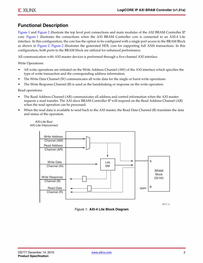
Functional DescriptionFigure 1 and Figure 2 illustrate the top level port connections and main modules of the AXI BRAM Controller IPcore. Figure 1 illustrates the connections when the AXI BRAM Controller core is connected to an AXI-4 Liteinterface. In this configuration, the core has the option to be configured with a single port access to the BRAM Blockas shown in Figure 2. Figure 2 illustrates the generated HDL core for supporting full AXI4 transactions. In thisconfiguration, both ports to the BRAM block are utilized for enhanced performance.
All communication with AXI master devices is performed through a five-channel AXI interface.
Write Operations:
• All write operations are initiated on the Write Address Channel (AW) of the AXI interface which specifies the type of write transaction and the corresponding address information.
• The Write Data Channel (W) communicates all write data for the single or burst write operations.
• The Write Response Channel (B) is used as the handshaking or response on the write operation.
Read operations:
• The Read Address Channel (AR) communicates all address and control information when the AXI master requests a read transfer. The AXI slave BRAM Controller IP will respond on the Read Address Channel (AR) when the read operation can be processed.
• When the read data is available to send back to the AXI master, the Read Data Channel (R) translates the data and status of the operation.
X-Ref Target - Figure 1
Figure 1: AXI-4 Lite Block Diagram
AXI-Lite Bus/AXI-Lite Interconnect
Write Address Channel (AW)
Read Address Channel (AR)
Write Response Channel (B)
Read Data Channel (R)
A
B
Write Data Channel (W)
DS777_01
BRAMBlock
(32-bit)
LiteSM
open

DS777 December 14, 2010 www.xilinx.com 3Product Specification
LogiCORE IP AXI BRAM Controller (v1.01a)
AXI4 Compatibility
The AXI BRAM Controller IP core is compliant to the AMBA® AXI4 interface specifications listed in the ReferenceDocuments section. The AXI BRAM Controller core includes the following features and exceptions.
• Support for 32-, 64-, and 128-bit BRAM data widths
• Support for all AXI 4 burst types and sizes
• The AXI BRAM Controller handles FIXED bursts as INCR type burst operations (no FIFO burst type capability in BRAM core)
• 16 beats for WRAP bursts
• 16 beats for FIXED bursts (treated as INCR burst type)
• 256 beats for INCR burst (w/o exclusive access)
• Support for burst sizes that are less than the width of the BRAM, for example narrow bursts. Data transfers are on different byte lanes for each beat of the burst.
• AXI user signals are not necessary or supported
• The AXI BRAM Controller executes all transactions in order regardless of thread ID value. No read reordering or write reordering is implemented.
• No caching or buffering functionality supported in the AXI BRAM Controller
X-Ref Target - Figure 2
Figure 2: AXI-4 Block Diagram
WriteChannel
SM
WriteDataReg
Write Address PipelineAXI Bus/AXI Interconnect
Write Address Channel (AW)
Read Address Channel (AR)
Write Response Channel (B)
Write Data Channel (W)
Read Data Channel (R)
Read Address Pipeline
Read Data Skid Buffer
AddrGen
BEGen
A
B
DS777_02
ReadChannel
SM
BRAMBlock
(32-bit, 64-bit, or 128-bit)
AddrGen
DS777 December 14, 2010 www.xilinx.com 4Product Specification
LogiCORE IP AXI BRAM Controller (v1.01a)
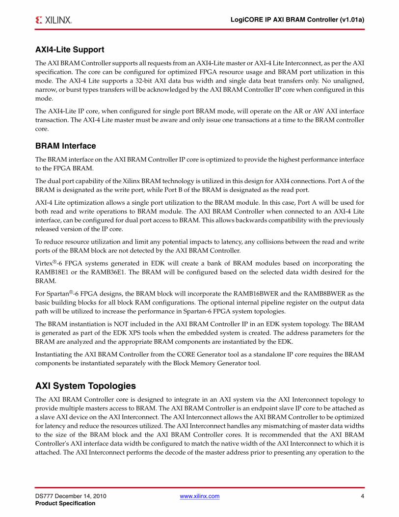
AXI4-Lite Support
The AXI BRAM Controller supports all requests from an AXI4-Lite master or AXI-4 Lite Interconnect, as per the AXIspecification. The core can be configured for optimized FPGA resource usage and BRAM port utilization in thismode. The AXI-4 Lite supports a 32-bit AXI data bus width and single data beat transfers only. No unaligned,narrow, or burst types transfers will be acknowledged by the AXI BRAM Controller IP core when configured in thismode.
The AXI4-Lite IP core, when configured for single port BRAM mode, will operate on the AR or AW AXI interfacetransaction. The AXI-4 Lite master must be aware and only issue one transactions at a time to the BRAM controllercore.
BRAM Interface
The BRAM interface on the AXI BRAM Controller IP core is optimized to provide the highest performance interfaceto the FPGA BRAM.
The dual port capability of the Xilinx BRAM technology is utilized in this design for AXI4 connections. Port A of theBRAM is designated as the write port, while Port B of the BRAM is designated as the read port.
AXI-4 Lite optimization allows a single port utilization to the BRAM module. In this case, Port A will be used forboth read and write operations to BRAM module. The AXI BRAM Controller when connected to an AXI-4 Liteinterface, can be configured for dual port access to BRAM. This allows backwards compatibility with the previouslyreleased version of the IP core.
To reduce resource utilization and limit any potential impacts to latency, any collisions between the read and writeports of the BRAM block are not detected by the AXI BRAM Controller.
Virtex®-6 FPGA systems generated in EDK will create a bank of BRAM modules based on incorporating theRAMB18E1 or the RAMB36E1. The BRAM will be configured based on the selected data width desired for theBRAM.
For Spartan®-6 FPGA designs, the BRAM block will incorporate the RAMB16BWER and the RAMB8BWER as thebasic building blocks for all block RAM configurations. The optional internal pipeline register on the output datapath will be utilized to increase the performance in Spartan-6 FPGA system topologies.
The BRAM instantiation is NOT included in the AXI BRAM Controller IP in an EDK system topology. The BRAMis generated as part of the EDK XPS tools when the embedded system is created. The address parameters for theBRAM are analyzed and the appropriate BRAM components are instantiated by the EDK.
Instantiating the AXI BRAM Controller from the CORE Generator tool as a standalone IP core requires the BRAMcomponents be instantiated separately with the Block Memory Generator tool.
AXI System TopologiesThe AXI BRAM Controller core is designed to integrate in an AXI system via the AXI Interconnect topology toprovide multiple masters access to BRAM. The AXI BRAM Controller is an endpoint slave IP core to be attached asa slave AXI device on the AXI Interconnect. The AXI Interconnect allows the AXI BRAM Controller to be optimizedfor latency and reduce the resources utilized. The AXI Interconnect handles any mismatching of master data widthsto the size of the BRAM block and the AXI BRAM Controller cores. It is recommended that the AXI BRAMController's AXI interface data width be configured to match the native width of the AXI Interconnect to which it isattached. The AXI Interconnect performs the decode of the master address prior to presenting any operation to the

DS777 December 14, 2010 www.xilinx.com 5Product Specification
LogiCORE IP AXI BRAM Controller (v1.01a)
AXI BRAM Controller core. Additional information on the Xilinx AXI Interconnect is available in ReferenceDocuments, page 36.
The connection of the AXI BRAM Controller core into an example system topology is shown in Figure 3 for bothAXI4 systems and an AXI-4 Lite system.
I/O Signals
X-Ref Target - Figure 3
Figure 3: AXI System Configuration
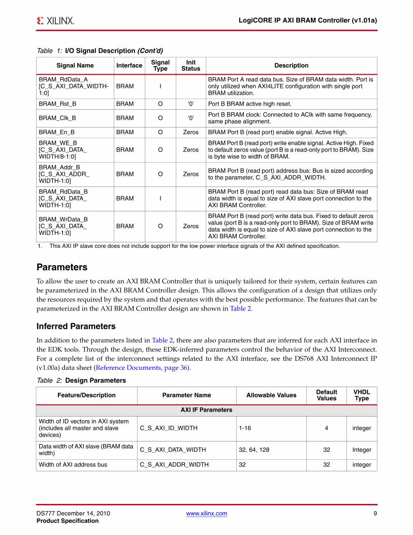
Table 1: I/O Signal Description
Signal Name Interface Signal Type
Init Status Description
Global Signals
S_AXI_ACLK Global I AXI Bus Clock.
S_AXI_ARESETN Global I AXI active low reset.
AXI Write Address Channel Signals (AW)
BRAM(configured as32-bit, 64-bit,
or 128-bit)
AXI BRAMController
AXISlave
AXIMaster
AXIMaster
A
BM S
S
M
DS777_03
Xilinx AXIInterconnect
AXI BRAMController
AXI-LiteMaster
AM SXilinx
AXI-LiteInterconnect
AXISlave
S
Bopen
32-bitBRAM
AXI4 System
AXI4-Lite System
DS777 December 14, 2010 www.xilinx.com 6Product Specification
LogiCORE IP AXI BRAM Controller (v1.01a)
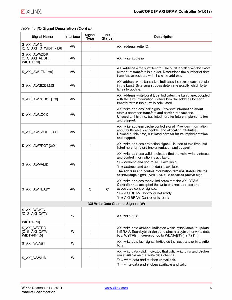
S_AXI_AWID [C_S_AXI_ID_WIDTH-1:0] AW I AXI address write ID.
S_AXI_AWADDR [C_S_AXI_ADDR_WIDTH-1:0]
AW I AXI write address
S_AXI_AWLEN [7:0] AW IAXI address write burst length: The burst length gives the exact number of transfers in a burst. Determines the number of data transfers associated with the write address.
S_AXI_AWSIZE [2:0] AW IAXI address write burst size: Indicates the size of each transfer in the burst. Byte lane strobes determine exactly which byte lanes to update.
S_AXI_AWBURST [1:0] AW IAXI address write burst type: Indicates the burst type, coupled with the size information, details how the address for each transfer within the burst is calculated.
S_AXI_AWLOCK AW I
AXI write address lock signal: Provides information about atomic operation transfers and barrier transactions. Unused at this time, but listed here for future implementation and support.
S_AXI_AWCACHE [4:0] AW I
AXI write address cache control signal: Provides information about bufferable, cacheable, and allocation attributes. Unused at this time, but listed here for future implementation and support.
S_AXI_AWPROT [3:0] AW I AXI write address protection signal: Unused at this time, but listed here for future implementation and support.
S_AXI_AWVALID AW I
AXI write address valid: Indicates that the valid write address and control information is available.‘0’ = address and control NOT available‘1’ = address and control data is availableThe address and control information remains stable until the acknowledge signal (AWREADY) is asserted (active high).
S_AXI_AWREADY AW O ‘0’
AXI write address ready: Indicates that the AXI BRAM Controller has accepted the write channel address and associated control signals.‘0’ = AXI BRAM Controller not ready‘1’ = AXI BRAM Controller is ready
AXI Write Data Channel Signals (W)
S_AXI_WDATA [C_S_AXI_DATA_
WIDTH-1:0]
W I AXI write data.
S_AXI_WSTRB [C_S_AXI_DATA_WIDTH/8-1:0]
W IAXI write data strobes: Indicates which bytes lanes to update in BRAM. Each byte strobe correlates to a byte other write data bus. WSTRB[n] corresponds to WDATA[(8*n) + 7:(8*n)].
S_AXI_WLAST W I AXI write data last signal: Indicates the last transfer in a write burst.
S_AXI_WVALID W I
AXI write data valid: Indicates that valid write data and strobes are available on the write data channel.‘0’ = write data and strobes unavailable‘1’ = write data and strobes available and valid
Table 1: I/O Signal Description (Cont’d)
Signal Name Interface Signal Type
Init Status Description

DS777 December 14, 2010 www.xilinx.com 7Product Specification
LogiCORE IP AXI BRAM Controller (v1.01a)
S_AXI_WREADY W O ‘0’
AXI write data ready: indicates that the AXI BRAM Controller is ready to accept the write data and strobes.‘0’ = AXI BRAM Controller not ready‘1’ = AXI BRAM Controller is ready
AXI Write Response Channel Signals (B)
S_AXI_BID [C_S_AXI_ID_WIDTH-1:0] B O Zeros
AXI write data response ID: Identification tab of the write response. BID matches the AWID value of the write transaction to which the AXI BRAM Controller is responding.
S_AXI_BRESP [1:0] B O Zeros
AXI write response: Indicates the status of the write transaction. The supported responses of the AXI BRAM Controller are OKAY (SLVERR and EXOKAY to be supported in a future release).
S_AXI_BVALID B O ‘0’
AXI write response valid: Asserted by the AXI BRAM Controller to indicate a valid write response is available.‘0’ = write response not available‘1’ = write response is available
S_AXI_BREADY B I
Write response ready: Indicates the master requesting the write operation can accept the response information.‘0’ = AXI master not ready‘1’ = AXI master is ready
AXI Read Address Channel Signals (AR)
S_AXI_ARID [C_S_AXI_ID_WIDTH-1:0] AR I AXI address read ID: Identification tag for the read address
group of signals.
S_AXI_ARADDR [C_S_AXI_ADDR_WIDTH-1:0]
AR I
AXI read address: The address provides the initial address of the read burst transaction. Only the start address of the burst is provided and the control signals indicate the address detail and calculation for each transfer in the burst.
S_AXI_ARLEN [7:0] AR IAXI address read burst length: The burst length gives the exact number of transfers in a burst. Determines the number of data transfers associated with the read address.
S_AXI_ARSIZE [2:0] AR I AXI address read burst size: Indicates the size of each transfer in the burst.
S_AXI_ARBURST [1:0] AR IAXI address read burst type: Indicates the burst type, coupled with the size information, details how the address for each transfer within the burst is calculated.
S_AXI_ARLOCK AR IAXI read address lock signal: Provides information about atomic operation transfers. Unused at this time, but listed here for future implementation and support.
S_AXI_ARCACHE [4:0] AR I
AXI read address cache control signa: Provides information about bufferable, cacheable, and allocation attributes. Unused at this time, but listed here for future implementation and support.
S_AXI_ARPROT [3:0] AR I AXI read address protection signal: Unused at this time, but listed here for future implementation and support.
Table 1: I/O Signal Description (Cont’d)
Signal Name Interface Signal Type
Init Status Description
DS777 December 14, 2010 www.xilinx.com 8Product Specification
LogiCORE IP AXI BRAM Controller (v1.01a)
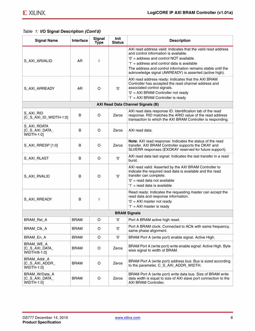
S_AXI_ARVALID AR I
AXI read address valid: Indicates that the valid read address and control information is available.‘0’ = address and control NOT available‘1’ = address and control data is availableThe address and control information remains stable until the acknowledge signal (AWREADY) is asserted (active high).
S_AXI_ARREADY AR O ‘0’
AXI read address ready: Indicates that the AXI BRAM Controller has accepted the read channel address and associated control signals.‘0’ = AXI BRAM Controller not ready‘1’ = AXI BRAM Controller is ready
AXI Read Data Channel Signals (B)
S_AXI_RID [C_S_AXI_ID_WIDTH-1:0] B O Zeros
AXI read data response ID: Identification tab of the read response. RID matches the ARID value of the read address transaction to which the AXI BRAM Controller is responding.
S_AXI_RDATA [C_S_AXI_DATA_WIDTH-1:0]
B O Zeros AXI read data.
S_AXI_RRESP [1:0] B O ZerosNote: AXI read response: Indicates the status of the read transfer. AXI BRAM Controller supports the OKAY and SLVERR responses (EXOKAY reserved for future support).
S_AXI_RLAST B O ‘0’ AXI read data last signal: Indicates the last transfer in a read burst.
S_AXI_RVALID B O ‘0’
AXI read valid: Asserted by the AXI BRAM Controller to indicate the required read data is available and the read transfer can complete.‘0’ = read data not available‘1’ = read data is available
S_AXI_RREADY B I
Read ready: Indicates the requesting master can accept the read data and response information.‘0’ = AXI master not ready‘1’ = AXI master is ready
BRAM Signals
BRAM_Rst_A BRAM O ‘0’ Port A BRAM active high reset.
BRAM_Clk_A BRAM O ‘0’ Port A BRAM clock: Connected to AClk with same frequency, same phase alignment.
BRAM_En_A BRAM O ‘0’ BRAM Port A (write port) enable signal. Active High.
BRAM_WE_A [C_S_AXI_DATA_WIDTH/8-1:0]
BRAM O Zeros BRAM Port A (write port) write enable signal: Active High. Byte wise signal to width of BRAM.
BRAM_Addr_A [C_S_AXI_ADDR_WIDTH-1:0]
BRAM O Zeros BRAM Port A (write port) address bus: Bus is sized according to the parameter, C_S_AXI_ADDR_WIDTH.
BRAM_WrData_A [C_S_AXI_DATA_WIDTH-1:0]
BRAM O ZerosBRAM Port A (write port) write data bus. Size of BRAM write data width is equal to size of AXI slave port connection to the AXI BRAM Controller.
Table 1: I/O Signal Description (Cont’d)
Signal Name Interface Signal Type
Init Status Description
DS777 December 14, 2010 www.xilinx.com 9Product Specification
LogiCORE IP AXI BRAM Controller (v1.01a)
ParametersTo allow the user to create an AXI BRAM Controller that is uniquely tailored for their system, certain features canbe parameterized in the AXI BRAM Controller design. This allows the configuration of a design that utilizes onlythe resources required by the system and that operates with the best possible performance. The features that can beparameterized in the AXI BRAM Controller design are shown in Table 2.
Inferred Parameters
In addition to the parameters listed in Table 2, there are also parameters that are inferred for each AXI interface inthe EDK tools. Through the design, these EDK-inferred parameters control the behavior of the AXI Interconnect.For a complete list of the interconnect settings related to the AXI interface, see the DS768 AXI Interconnect IP(v1.00a) data sheet (Reference Documents, page 36).
BRAM_RdData_A [C_S_AXI_DATA_WIDTH-1:0]
BRAM IBRAM Port A read data bus. Size of BRAM data width. Port is only utilized when AXI4LITE configuration with single port BRAM utilization.
BRAM_Rst_B BRAM O ‘0’ Port B BRAM active high reset.
BRAM_Clk_B BRAM O ‘0’ Port B BRAM clock: Connected to AClk with same frequency, same phase alignment.
BRAM_En_B BRAM O Zeros BRAM Port B (read port) enable signal. Active High.
BRAM_WE_B [C_S_AXI_DATA_WIDTH/8-1:0]
BRAM O ZerosBRAM Port B (read port) write enable signal. Active High. Fixed to default zeros value (port B is a read-only port to BRAM). Size is byte wise to width of BRAM.
BRAM_Addr_B [C_S_AXI_ADDR_WIDTH-1:0]
BRAM O Zeros BRAM Port B (read port) address bus: Bus is sized according to the parameter, C_S_AXI_ADDR_WIDTH.
BRAM_RdData_B [C_S_AXI_DATA_WIDTH-1:0]
BRAM IBRAM Port B (read port) read data bus: Size of BRAM read data width is equal to size of AXI slave port connection to the AXI BRAM Controller.
BRAM_WrData_B [C_S_AXI_DATA_WIDTH-1:0]
BRAM O Zeros
BRAM Port B (read port) write data bus. Fixed to default zeros value (port B is a read-only port to BRAM). Size of BRAM write data width is equal to size of AXI slave port connection to the AXI BRAM Controller.
1. This AXI IP slave core does not include support for the low power interface signals of the AXI defined specification.
Table 2: Design Parameters
Feature/Description Parameter Name Allowable Values Default Values
VHDL Type
AXI IF Parameters
Width of ID vectors in AXI system (includes all master and slave devices)
C_S_AXI_ID_WIDTH 1-16 4 integer
Data width of AXI slave (BRAM data width) C_S_AXI_DATA_WIDTH 32, 64, 128 32 Integer
Width of AXI address bus C_S_AXI_ADDR_WIDTH 32 32 integer
Table 1: I/O Signal Description (Cont’d)
Signal Name Interface Signal Type
Init Status Description

DS777 December 14, 2010 www.xilinx.com 10Product Specification
LogiCORE IP AXI BRAM Controller (v1.01a)
Set by EDK tools depending on system configuration and AXI bus type connected to core.
C_S_AXI_PROTOCOL AXI4, AXI4LITE AXI4 string
Support of AXI narrow write or read operations. Only valid when connected to full AXI4 interface.
C_S_AXI_SUPPORTS_NARROW_BURST
0 = No support for narrow AXI transactions1 = Core includes logic to support narrow transfers
1 integer
Selects if AXI BRAM Controller can utilize and be optimized in size for utilizing a single port to BRAM. Only allowable when AXI4LITE mode is selected.
C_SINGLE_PORT_BRAM
0 = Core utilizes both BRAM ports (available in both AXI4 and AXI4-Lite mode)1 = Only allowable when AXI4LITE mode, uses single port to BRAM
0 integer
Non HDL Parameters (Not included in RTL, but integrated as a part of the core during
the EDK build process to allow for AXI system optimizations)
AXI BRAM base address assignment
C_S_AXI_BASEADDR (1)(2)
System address value of C_AWIDTH bits wide FFFF_FFFF std_logic
_vector
AXI BRAM high address assignment
C_S_AXI_HIGHADDR (1)(2)
System address value of C_AWIDTH bits wide 0000_0000 std_logic
_vector
Maximum number of active write transactions that the AXI slave can accept. (sets the parameter, WRITE_ISSUING in the AXI Interconnect)
C_INTERCONNECT_S_AXI_WRITE_ACCEPTANCE
2 (set constant) for AXI41 (default) for AXI4LITE
1 integer
Maximum number of active read transactions that the AXI slave can accept.
C_INTERCONNECT_S_AXI_READ_ACCEPTANCE
2 (set constant) for AXI41 (default) for AXI4LITE
1 integer
Indicates (for Interconnect) if AXI AR channel registers are enabled.
C_INTERCONNECT_S_AXI_AR_REGISTER 0, 1 1 integer
Indicates (for Interconnect) if AXI AW channel registers are enabled.
C_INTERCONNECT_S_AXI_AW_REGISTER 0, 1 1 integer
Indicates (for Interconnect) if AXI W channel registers are enabled.
C_INTERCONNECT_S_AXI_W_REGISTER 0, 1 1 integer
Indicates (for Interconnect) if AXI B channel registers are enabled.
C_INTERCONNECT_S_AXI_B_REGISTER 0, 1 1 integer
Indicates (for Interconnect) if AXI R channel registers are enabled.
C_INTERCONNECT_S_AXI_R_REGISTER 0, 1 1 integer
Target FPGA Family Parameter
Target FPGA device family C_FAMILY spartan6, virtex6 virtex6 string
1. Default values are specified for C_S_AXI_BASEADDR and C_S_AXI_HIGHADDR to ensure that they are set by the user. If the value is not set, an implementation error will be generated.
2. C_S_AXI_BASEADDR and C_S_AXI_HIGHADDR must be a power of 2 and specify a continuous address space.
Table 2: Design Parameters (Cont’d)
Feature/Description Parameter Name Allowable Values Default Values
VHDL Type
DS777 December 14, 2010 www.xilinx.com 11Product Specification
LogiCORE IP AXI BRAM Controller (v1.01a)
Parameter - I/O Signal Dependencies
Addressing ConfigurationsTable 4 illustrates some example settings for C_S_AXI_BASEADDR and C_S_AXI_HIGHADDR to create a specificsize of BRAM in the system. The range specified by the base and high address parameters must be a continuousaddress space and be equal to 2n bytes minus 1, where n is a positive integer and 2n is a valid memory size for theBRAM available in the FPGA device family.
Table 3: Parameter-I/O Signal Dependencies
Generic Name Affects Port Depends on Parameter Relationship Description
C_S_AXI_ID_WIDTH AWID, BID, ARID, RID Port widths are set directly from the parameter value.
C_S_AXI_DATA_WIDTH
WDATA, WSTRB, RDATA,BRAM_WE_A, BRAM_WrData_A,BRAM_RdData_A,BRAM_RdData_B
Port widths are set directly from the parameter value.
C_S_AXI_ADDR_WIDTHAWADDR, ARADDR, BRAM_Addr_A, BRAM_Addr_B
Port widths are set directly or derived from the parameter value.
C_S_AXI_SUPPORTS_NARROW_BURST C_S_AXI_PROTOCOL Narrow bursts can only be enabled
when bus set for AXI4.
C_SINGLE_PORT_BRAM C_S_AXI_PROTOCOLSingle port BRAM configuration is only allowable when connected to AXI4LITE.
Table 4: Example Address Ranges
Memory Size (Bytes) Basic Address Range Required Example
C_S_AXI_BASEADDRExample
C_S_AXI_HIGHADDR
4k 0x0000_0000 to 0x0000_0FFF 0xA000 0000 0xA000 0FFF
8k 0x0000_0000 to 0x0000_1FFF 0x2400 0000 0x2400 1FFF
16k 0x0000_0000 to 0x0000_3FFF 0x1F00 0000 0x1F00 3FFF
32k 0x0000_0000 to 0x0000_7FFF 0x3000 0000 0x3000 7FFF
64k 0x0000_0000 to 0x0000_FFFF 0xB000 0000 0xB000 FFFF
128k 0x0000_0000 to 0x0001_FFFF 0x2000 0000 0x2001 FFFF
256k 0x0000_0000 to 0x0003_FFFF 0xFFFC 0000 0xFFFF FFFF
DS777 December 14, 2010 www.xilinx.com 12Product Specification
LogiCORE IP AXI BRAM Controller (v1.01a)
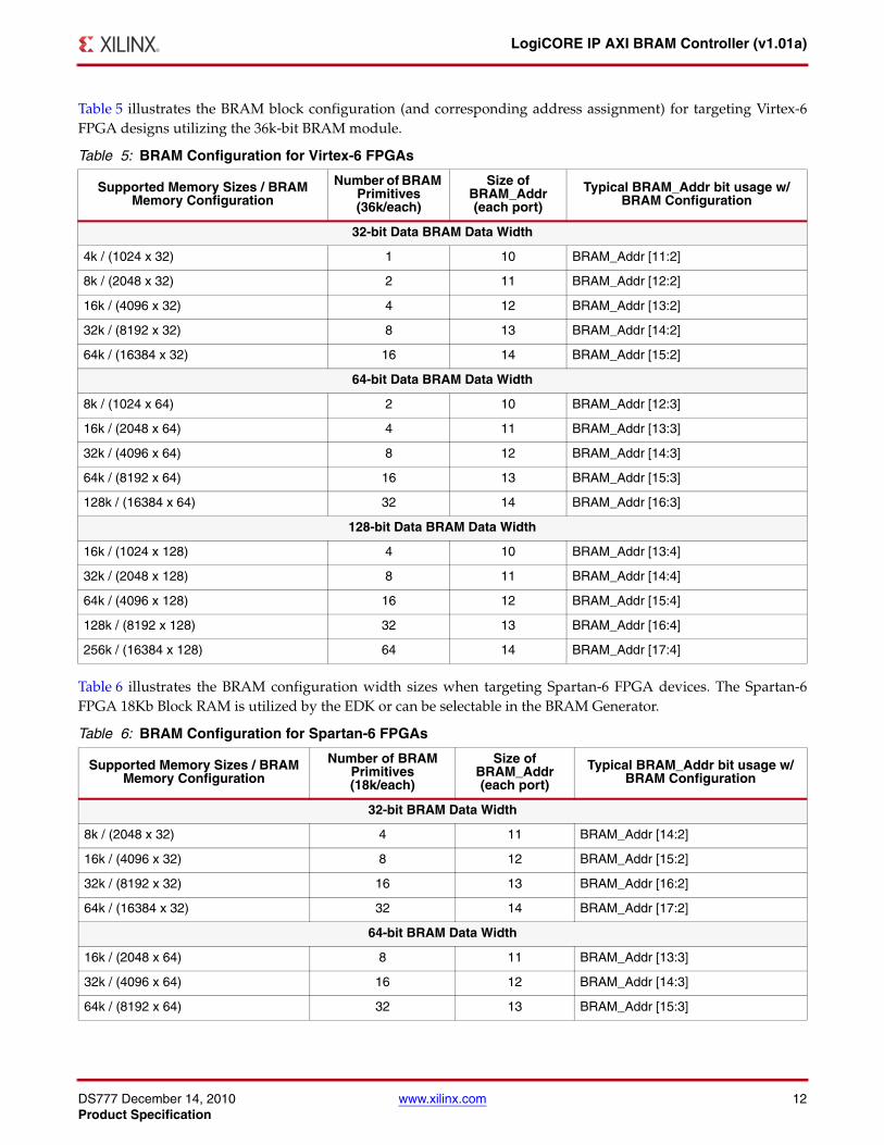
Table 5 illustrates the BRAM block configuration (and corresponding address assignment) for targeting Virtex-6FPGA designs utilizing the 36k-bit BRAM module.
Table 6 illustrates the BRAM configuration width sizes when targeting Spartan-6 FPGA devices. The Spartan-6FPGA 18Kb Block RAM is utilized by the EDK or can be selectable in the BRAM Generator.
Table 5: BRAM Configuration for Virtex-6 FPGAs
Supported Memory Sizes / BRAM Memory Configuration
Number of BRAM Primitives (36k/each)
Size of BRAM_Addr (each port)
Typical BRAM_Addr bit usage w/ BRAM Configuration
32-bit Data BRAM Data Width
4k / (1024 x 32) 1 10 BRAM_Addr [11:2]
8k / (2048 x 32) 2 11 BRAM_Addr [12:2]
16k / (4096 x 32) 4 12 BRAM_Addr [13:2]
32k / (8192 x 32) 8 13 BRAM_Addr [14:2]
64k / (16384 x 32) 16 14 BRAM_Addr [15:2]
64-bit Data BRAM Data Width
8k / (1024 x 64) 2 10 BRAM_Addr [12:3]
16k / (2048 x 64) 4 11 BRAM_Addr [13:3]
32k / (4096 x 64) 8 12 BRAM_Addr [14:3]
64k / (8192 x 64) 16 13 BRAM_Addr [15:3]
128k / (16384 x 64) 32 14 BRAM_Addr [16:3]
128-bit Data BRAM Data Width
16k / (1024 x 128) 4 10 BRAM_Addr [13:4]
32k / (2048 x 128) 8 11 BRAM_Addr [14:4]
64k / (4096 x 128) 16 12 BRAM_Addr [15:4]
128k / (8192 x 128) 32 13 BRAM_Addr [16:4]
256k / (16384 x 128) 64 14 BRAM_Addr [17:4]
Table 6: BRAM Configuration for Spartan-6 FPGAs
Supported Memory Sizes / BRAM Memory Configuration
Number of BRAM Primitives(18k/each)
Size of BRAM_Addr (each port)
Typical BRAM_Addr bit usage w/ BRAM Configuration
32-bit BRAM Data Width
8k / (2048 x 32) 4 11 BRAM_Addr [14:2]
16k / (4096 x 32) 8 12 BRAM_Addr [15:2]
32k / (8192 x 32) 16 13 BRAM_Addr [16:2]
64k / (16384 x 32) 32 14 BRAM_Addr [17:2]
64-bit BRAM Data Width
16k / (2048 x 64) 8 11 BRAM_Addr [13:3]
32k / (4096 x 64) 16 12 BRAM_Addr [14:3]
64k / (8192 x 64) 32 13 BRAM_Addr [15:3]
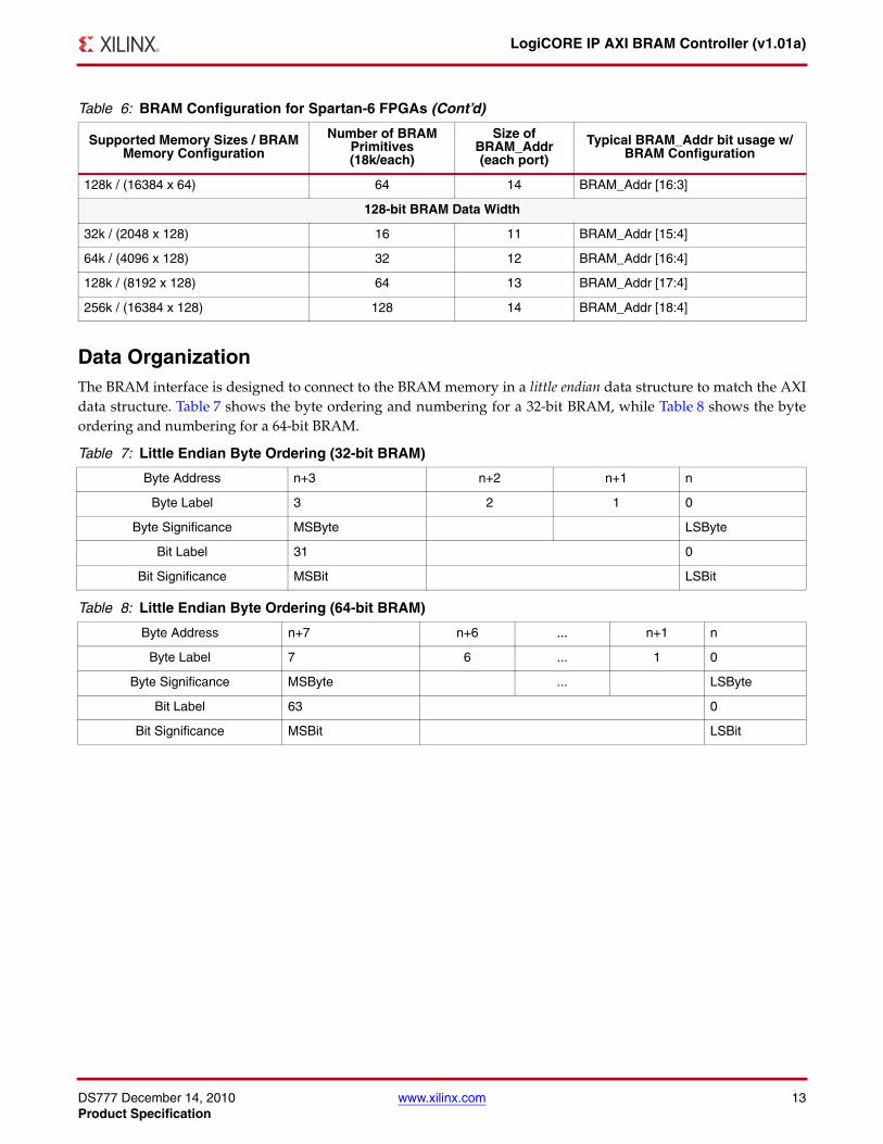
DS777 December 14, 2010 www.xilinx.com 13Product Specification
LogiCORE IP AXI BRAM Controller (v1.01a)
Data OrganizationThe BRAM interface is designed to connect to the BRAM memory in a little endian data structure to match the AXIdata structure. Table 7 shows the byte ordering and numbering for a 32-bit BRAM, while Table 8 shows the byteordering and numbering for a 64-bit BRAM.
128k / (16384 x 64) 64 14 BRAM_Addr [16:3]
128-bit BRAM Data Width
32k / (2048 x 128) 16 11 BRAM_Addr [15:4]
64k / (4096 x 128) 32 12 BRAM_Addr [16:4]
128k / (8192 x 128) 64 13 BRAM_Addr [17:4]
256k / (16384 x 128) 128 14 BRAM_Addr [18:4]
Table 7: Little Endian Byte Ordering (32-bit BRAM)
Byte Address n+3 n+2 n+1 n
Byte Label 3 2 1 0
Byte Significance MSByte LSByte
Bit Label 31 0
Bit Significance MSBit LSBit
Table 8: Little Endian Byte Ordering (64-bit BRAM)
Byte Address n+7 n+6 ... n+1 n
Byte Label 7 6 ... 1 0
Byte Significance MSByte ... LSByte
Bit Label 63 0
Bit Significance MSBit LSBit
Table 6: BRAM Configuration for Spartan-6 FPGAs (Cont’d)
Supported Memory Sizes / BRAM Memory Configuration
Number of BRAM Primitives(18k/each)
Size of BRAM_Addr (each port)
Typical BRAM_Addr bit usage w/ BRAM Configuration
DS777 December 14, 2010 www.xilinx.com 14Product Specification
LogiCORE IP AXI BRAM Controller (v1.01a)
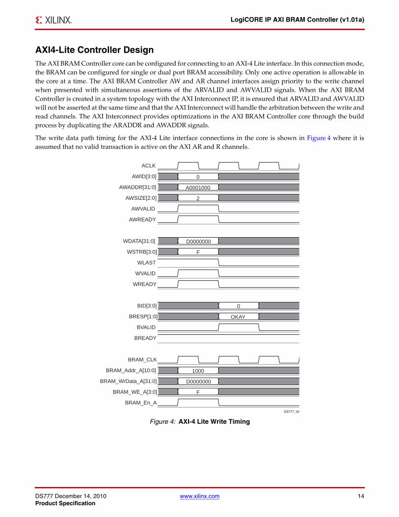
AXI4-Lite Controller DesignThe AXI BRAM Controller core can be configured for connecting to an AXI-4 Lite interface. In this connection mode,the BRAM can be configured for single or dual port BRAM accessibility. Only one active operation is allowable inthe core at a time. The AXI BRAM Controller AW and AR channel interfaces assign priority to the write channelwhen presented with simultaneous assertions of the ARVALID and AWVALID signals. When the AXI BRAMController is created in a system topology with the AXI Interconnect IP, it is ensured that ARVALID and AWVALIDwill not be asserted at the same time and that the AXI Interconnect will handle the arbitration between the write andread channels. The AXI Interconnect provides optimizations in the AXI BRAM Controller core through the buildprocess by duplicating the ARADDR and AWADDR signals.
The write data path timing for the AXI-4 Lite interface connections in the core is shown in Figure 4 where it isassumed that no valid transaction is active on the AXI AR and R channels.X-Ref Target - Figure 4
Figure 4: AXI-4 Lite Write Timing
ACLK
AWID[3:0]
AWADDR[31:0]
AWSIZE[2:0]
AWVALID
AWREADY
WDATA[31:0]
WSTRB[3:0]
WLAST
WVALID
WREADY
BID[3:0]
BRESP[1:0]
BVALID
BREADY
BRAM_CLK
BRAM_Addr_A[10:0]
BRAM_WrData_A[31:0]
BRAM_WE_A[3:0]
BRAM_En_A
0
A0001000
2
D0000000
F
0
OKAY
1000
D0000000
F
DS777_04
DS777 December 14, 2010 www.xilinx.com 15Product Specification
LogiCORE IP AXI BRAM Controller (v1.01a)
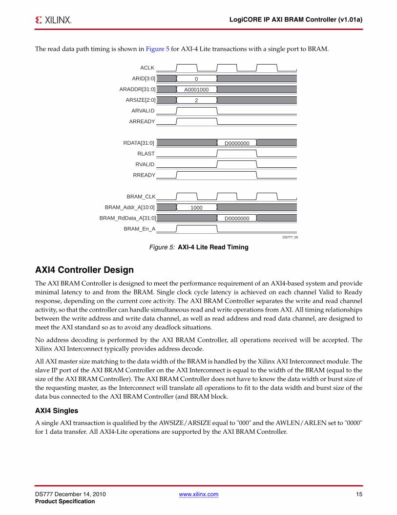
The read data path timing is shown in Figure 5 for AXI-4 Lite transactions with a single port to BRAM.
AXI4 Controller DesignThe AXI BRAM Controller is designed to meet the performance requirement of an AXI4-based system and provideminimal latency to and from the BRAM. Single clock cycle latency is achieved on each channel Valid to Readyresponse, depending on the current core activity. The AXI BRAM Controller separates the write and read channelactivity, so that the controller can handle simultaneous read and write operations from AXI. All timing relationshipsbetween the write address and write data channel, as well as read address and read data channel, are designed tomeet the AXI standard so as to avoid any deadlock situations.
No address decoding is performed by the AXI BRAM Controller, all operations received will be accepted. TheXilinx AXI Interconnect typically provides address decode.
All AXI master size matching to the data width of the BRAM is handled by the Xilinx AXI Interconnect module. Theslave IP port of the AXI BRAM Controller on the AXI Interconnect is equal to the width of the BRAM (equal to thesize of the AXI BRAM Controller). The AXI BRAM Controller does not have to know the data width or burst size ofthe requesting master, as the Interconnect will translate all operations to fit to the data width and burst size of thedata bus connected to the AXI BRAM Controller (and BRAM block.
AXI4 Singles
A single AXI transaction is qualified by the AWSIZE/ARSIZE equal to "000" and the AWLEN/ARLEN set to "0000"for 1 data transfer. All AXI4-Lite operations are supported by the AXI BRAM Controller.
X-Ref Target - Figure 5
Figure 5: AXI-4 Lite Read Timing
ACLK
ARID[3:0]
ARADDR[31:0]
ARSIZE[2:0]
ARVALID
ARREADY
RDATA[31:0]
RLAST
RVALID
RREADY
BRAM_CLK
BRAM_Addr_A[10:0]
BRAM_RdData_A[31:0]
BRAM_En_A
0
A0001000
2
D0000000
1000
D0000000
DS777_05

DS777 December 14, 2010 www.xilinx.com 16Product Specification
LogiCORE IP AXI BRAM Controller (v1.01a)
Bursting
All burst types presented to the AXI BRAM Controller are supported. However, fixed burst types are translated intoincrementing burst types issued to the BRAM. Wrapping burst types are support for processor cacheline read andwrites with BRAM.
Each burst is specified to have N data transfers (1-256 specified in AWLEN/ARLEN) of M bytes (1-128 bytesspecified in AWSIZE/ARSIZE). The AXI BRAM Controller will support up to the AXI4 extension on burst sizes to256 data beats.
The size of the burst must be equal or less than the size of the BRAM data width. For instance, 64-bit BRAM onlyallows bursts of up to 64 byte sizes. Burst sizes less than the full width of the AXI BRAM Controller data bus isreferred to as a narrow burst. All narrow bursts are supported by the AXI BRAM Controller − for example, when amaster is requesting a byte burst operation to or from a 64-bit data wide BRAM. For narrow bursts, the AXI protocoldefines that the valid byte lanes rotate through the correct byte lanes. In the AXI BRAM Controller, each write databeat of a burst on the AXI is translated to a write operation to the BRAM. The BRAM byte enables are configuredsuch that only the valid bytes are stored in memory. The AXI BRAM Controller does not buffer any subsize databeats into the full width to the BRAM. An example is shown in the section, Narrow Write Bursting, page 21.
Unaligned burst transfers are allowed and the AXI master must indicate this with the lower order bits of theaddress bus provided with the write address channel data handshaking. An example is shown in section,Unaligned Write Bursting, page 22. Unaligned burst transfers may also be indicated with an aligned address, butuse the write data channel data strobes to indicate the valid byte lanes.
Each write and read channel of the AXI BRAM Controller utilizes an address counter that is loaded at the beginningof the burst operation. AXI provides the starting address of the burst, and the AXI BRAM Controller increments theaddress based on the BRAM data width.
AXI does not allow any read nor write burst termination. Each AXI master must complete each burst transactionthat is initiated. Each burst transaction is complete when the LAST signal is asserted, by the master of writes, andby the AXI BRAM Controller on reads.
The write enables presented to the BRAM are calculated based on burst type, address offset of the write address,along with the AXI write data strobes. The write enables are generated on a per-byte basis to the BRAM. Writeenables are 4-bits wide for 32-bit BRAMs, 8-bits wide for 64-bit BRAMs and 16-bits wide for 128-bit BRAMinstantiations.
Cacheline
Cacheline operations are implemented as WRAP burst types on AXI when presented to the BRAM. The allowableburst sizes for WRAP bursts are 2, 4, 8, and 16 data transfers. The AWBURST/ARBURST must be set to "10" for theWRAP burst type.
WRAP bursts are handled in the address generator logic of the controller to the BRAM. The address seen by theBRAM must increment to the boundary, then wrap back around to the beginning of the cacheline address. Forexample, a processor issuing a target word first cache line read request to address, 0x04h. On a 32-bit BRAM, theBRAM will see the following sequence of address requested reads: 0x04h, 0x08h, 0x0Ch, 0x00h. This example isillustrated in Cacheline Reads, page 30 for a cacheline read.
Pipelining
Each write and read channel interface to the AXI is capable of holding two active addresses or operations. The AXIBRAM Controller IP allows two active write and two active read transactions to be captured and held. The dataprovided with each address channel operation must remain in order. No out of order operations are allowed in the

DS777 December 14, 2010 www.xilinx.com 17Product Specification
LogiCORE IP AXI BRAM Controller (v1.01a)
AXI BRAM Controller. The pipelining capability allows the same master or another master to request a subsequentwrite or read transaction. With the storage of multiple write addresses in the AXI BRAM Controller, the write datamay not be immediately captured and stored by the controller. The write data channel interface of the AXI BRAMController will not asserted WREADY until the BRAM is ready to accept the data of the pipelined write transaction.On the write address channel interface, the AXI BRAM Controller will keep AWREADY asserted, until the pipelinefull condition is reached. At this point, the AWREADY is negated and no further write addresses will be accepteduntil the 1st address data phase is complete and the 2nd pipelined address can be processed by the controller. Anexample of the timing relationship is shown in the section, Write Pipeline, page 23.
On read transactions, two-deep address pipelining is supported in the AXI BRAM Controller. The AXI BRAMController will issue the request to BRAM and provide data on the read data channel, as long as the requestingmaster asserts RREADY.
ID Wrapping
The AXI BRAM Controller does not support data reordering. All ID values are wrapped back around on the datachannel during handshaking. The AWID (on the write address channel) is captured and returned as the BID signal(of the write response channel) during the write data transaction. The ARID (on the read address channel) iscaptured and returned as the RID signal (of the read response channel) during the read data response transaction.
Power Considerations
To conserve power consumption on the BRAM interface, the BRAM enable signal is only asserted during activeread or write operations. The enable signal on each port to BRAM will be negated when there is no activity on theAXI bus.
AXI TimingThe timing diagrams shown in the subsequent sections represent the timing relationships of the AXI slave AXIBRAM Controller IP connection to the Xilinx AXI Interconnect. All write operations are initiated on the WriteAddress Channel (AW) of the AXI bus which specifies the type of write transaction and the corresponding addressinformation. The handshaking protocol follows a Valid and Ready mechanism. All address and control informationis only valid when the Valid signal is asserted. When the slave asserts the Ready signal, it captures the signals andaccepts the operation. The Write Data Channel (W) communicates all write data for the single or burst writeoperation. The Write Response Channel (B) is used as the handshaking or response on the write operation.
On read operations, the Read Address Channel (AR) communicates all address and control information when theAXI master asserts the Valid signal. The slave IP (or AXI BRAM Controller) asserts the Ready signal on the RACwhen the read operation can be processed. When the read data is available to send back to the AXI master, the ReadData Channel (R) translates the data and status of the operation.
AXI4 Single Operations
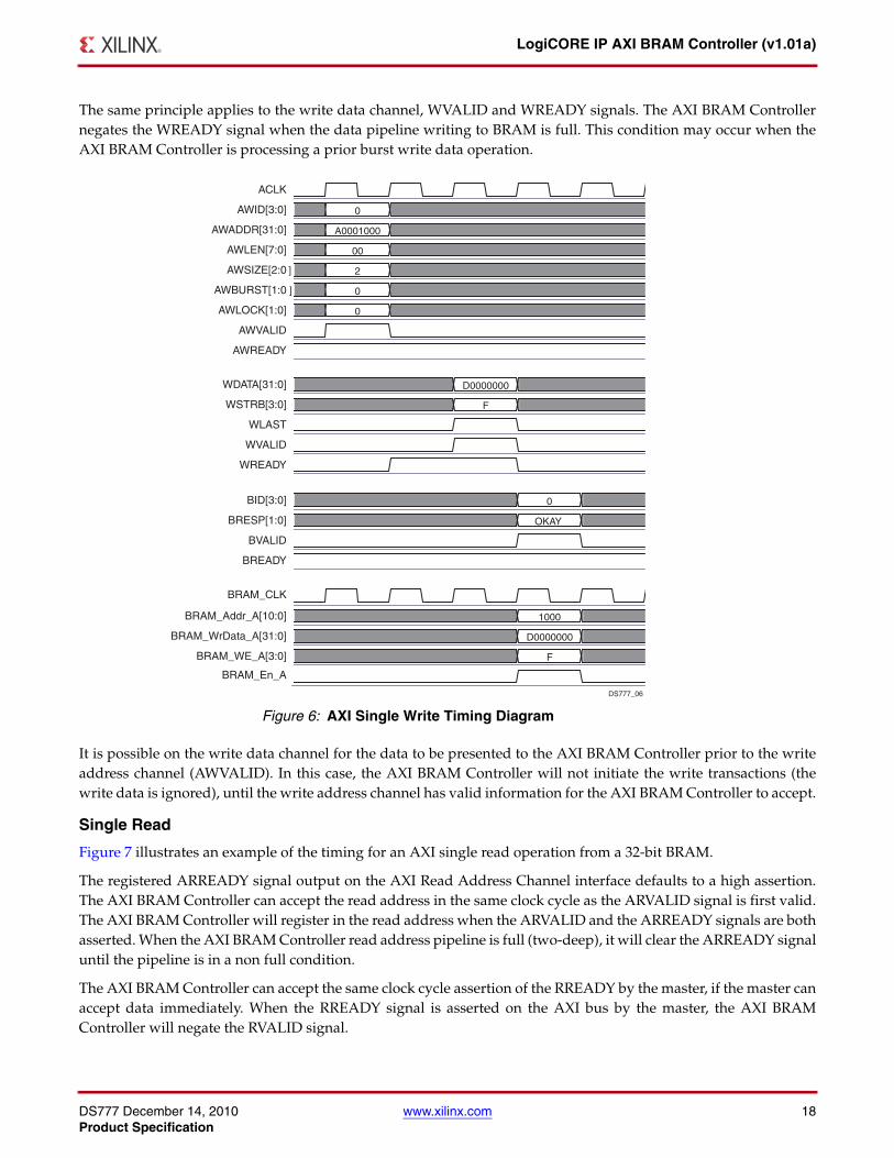
Single Write
Figure 6 illustrates an example for the timing of an AXI single 32-bit write operation to a 32-bit wide BRAM. Theexample illustrates the single write to BRAM address 0x1000h, provided that C_S_AXI_BASEADDR is set to0xA000 0000 and that the C_S_AXI_HIGHADDR allows space for more than 4 k of addressable BRAM.
As recommended, the AXI BRAM Controller keeps the AWREADY signal asserted on the bus, as the address can becaptured in the clock cycle when the AWVALID and AWREADY signals are both asserted. Once the write addresspipeline (two-deep) is full, the slave AXI BRAM Controller negates the AWREADY registered output signal.
DS777 December 14, 2010 www.xilinx.com 18Product Specification
LogiCORE IP AXI BRAM Controller (v1.01a)
The same principle applies to the write data channel, WVALID and WREADY signals. The AXI BRAM Controllernegates the WREADY signal when the data pipeline writing to BRAM is full. This condition may occur when theAXI BRAM Controller is processing a prior burst write data operation.
It is possible on the write data channel for the data to be presented to the AXI BRAM Controller prior to the writeaddress channel (AWVALID). In this case, the AXI BRAM Controller will not initiate the write transactions (thewrite data is ignored), until the write address channel has valid information for the AXI BRAM Controller to accept.
Single Read
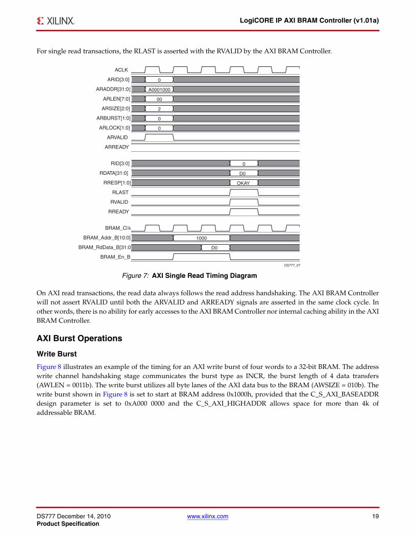
Figure 7 illustrates an example of the timing for an AXI single read operation from a 32-bit BRAM.
The registered ARREADY signal output on the AXI Read Address Channel interface defaults to a high assertion.The AXI BRAM Controller can accept the read address in the same clock cycle as the ARVALID signal is first valid.The AXI BRAM Controller will register in the read address when the ARVALID and the ARREADY signals are bothasserted. When the AXI BRAM Controller read address pipeline is full (two-deep), it will clear the ARREADY signaluntil the pipeline is in a non full condition.
The AXI BRAM Controller can accept the same clock cycle assertion of the RREADY by the master, if the master canaccept data immediately. When the RREADY signal is asserted on the AXI bus by the master, the AXI BRAMController will negate the RVALID signal.
X-Ref Target - Figure 6
Figure 6: AXI Single Write Timing Diagram
ACLK
AWID[3:0]
AWADDR[31:0]
AWLEN[7:0]
AWSIZE[2:0 ]
AWBURST[1:0 ]
AWLOCK[1:0]
AWVALID
AWREADY
WDATA[31:0]
WSTRB[3:0]
WLAST
WVALID
WREADY
BID[3:0]
BRESP[1:0]
BVALID
BREADY
BRAM_CLK
BRAM_Addr_A[10:0]
BRAM_WrData_A[31:0]
BRAM_WE_A[3:0]
BRAM_En_A
0
A0001000
00
2
0
0
D0000000
F
0
OKAY
1000
D0000000
F
DS777_06
DS777 December 14, 2010 www.xilinx.com 19Product Specification
LogiCORE IP AXI BRAM Controller (v1.01a)
For single read transactions, the RLAST is asserted with the RVALID by the AXI BRAM Controller.
On AXI read transactions, the read data always follows the read address handshaking. The AXI BRAM Controllerwill not assert RVALID until both the ARVALID and ARREADY signals are asserted in the same clock cycle. Inother words, there is no ability for early accesses to the AXI BRAM Controller nor internal caching ability in the AXIBRAM Controller.
AXI Burst Operations
Write Burst
Figure 8 illustrates an example of the timing for an AXI write burst of four words to a 32-bit BRAM. The addresswrite channel handshaking stage communicates the burst type as INCR, the burst length of 4 data transfers(AWLEN = 0011b). The write burst utilizes all byte lanes of the AXI data bus to the BRAM (AWSIZE = 010b). Thewrite burst shown in Figure 8 is set to start at BRAM address 0x1000h, provided that the C_S_AXI_BASEADDRdesign parameter is set to 0xA000 0000 and the C_S_AXI_HIGHADDR allows space for more than 4k ofaddressable BRAM.
X-Ref Target - Figure 7
Figure 7: AXI Single Read Timing Diagram
ACLK
ARID[3:0]
ARADDR[31:0]
ARLEN[7:0]
ARSIZE[2:0]
ARBURST[1:0]
ARLOCK[1:0]
ARVALID
ARREADY
RID[3:0]
RDATA[31:0]
RRESP[1:0]
RLAST
RVALID
RREADY
BRAM_Cl k
BRAM_Addr_B[10:0]
BRAM_RdData_B[31:0]
BRAM_En_B
0
A0001000
00
2
0
0
0
D0
OKAY
1000
D0
DS777_07

DS777 December 14, 2010 www.xilinx.com 20Product Specification
LogiCORE IP AXI BRAM Controller (v1.01a)
On the AXI write transactions, the slave does not wait for the write data channel, WVALID signal to be assertedprior to the assertion of the write address channel signal, AWREADY, which could potentially cause a deadlockcondition and is not allowed.X-Ref Target - Figure 8
Figure 8: AXI Burst Write Timing Diagram
ACLK
AWID[3:0]
AWADDR[31:0]
AWLEN[7:0]
AWSIZE[2:0 ]
AWBURST[1:0 ]
AWLOCK[1:0]
AWVALID
AWREADY
WDATA[31:0]
WSTRB[3:0]
WLAST
WVALID
WREADY
BID[3:0]
BRESP[1:0]
BVALID
BREADY
BRAM_CLK
BRAM_Addr_A[10:0]
BRAM_WrData_A[31:0]
BRAM_WE_A[3:0]
BRAM_En_A
0
A0001000
03
2
INCR
0
D0 D1 D2 D3
F F F F
0
OKAY
1000 1004 1008 100C
D0 D1 D2 D3
F F F F
DS777_08

DS777 December 14, 2010 www.xilinx.com 21Product Specification
LogiCORE IP AXI BRAM Controller (v1.01a)
Narrow Write Bursting
Figure 9 illustrates an example of the AXI BRAM Controller supporting a narrow burst operation. A narrow burst isdefined as a master bursting a data size smaller than the BRAM data width. If the burst type (AWBURST) is set toINCR or WRAP, the valid data on the BRAM interface to the AXI bus will rotate for each data beat. The AXI BRAMController handles each data beat on the AXI as a corresponding data beat to the BRAM, regardless of the smallervalid byte lanes. In this scenario, the AXI WSTRB is translated to the BRAM write enable signals. The BRAMaddress increments only when the full address (data) width boundary is met with the narrow write to BRAM.
The timing diagram illustrates an example of AXI narrow bursting with a 32-bit BRAM and the AXI master requestis a halfword burst of 4 data beats. AWSIZE is set to 001b.X-Ref Target - Figure 9
Figure 9: AXI Narrow Burst Write Diagram
ACLK
AWID[3:0]
AWADDR[31:0]
AWLEN[7:0]
AWSIZE[2:0]
AWBURST[1:0]
AWLOCK[1:0]
AWVALID
AWREADY
WDATA[31:0]
WSTRB[3:0]
WLAST
WVALID
WREADY
BID[3:0]
BRESP[1:0]
BVALID
BREADY
BRAM_Addr_A[10:0]
BRAM_WrData_A[31:0]
BRAM_WE_A[3:0]
BRAM_En_A
0
A0001000
03
1
INCR
0
D0D1D2D3 D0D1D2D3 D4D5D6D7 D4D5D6D7
C 3 C 3
0
OKAY
1000 1000 1004 1004
D0D10000 0000D2D3 D4D50000 0000D6D7
C 3 C 3
DS777_09
DS777 December 14, 2010 www.xilinx.com 22Product Specification
LogiCORE IP AXI BRAM Controller (v1.01a)
Unaligned Write Bursting
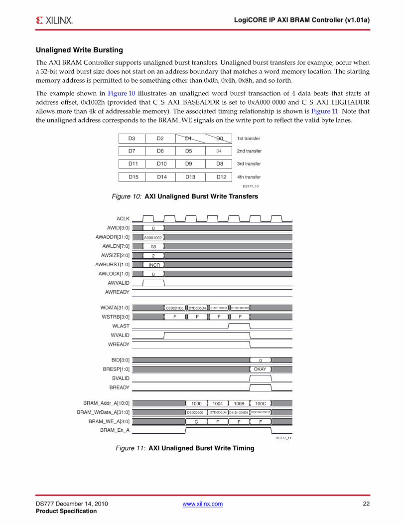
The AXI BRAM Controller supports unaligned burst transfers. Unaligned burst transfers for example, occur whena 32-bit word burst size does not start on an address boundary that matches a word memory location. The startingmemory address is permitted to be something other than 0x0h, 0x4h, 0x8h, and so forth.
The example shown in Figure 10 illustrates an unaligned word burst transaction of 4 data beats that starts ataddress offset, 0x1002h (provided that C_S_AXI_BASEADDR is set to 0xA000 0000 and C_S_AXI_HIGHADDRallows more than 4k of addressable memory). The associated timing relationship is shown is Figure 11. Note thatthe unaligned address corresponds to the BRAM_WE signals on the write port to reflect the valid byte lanes.X-Ref Target - Figure 10
Figure 10: AXI Unaligned Burst Write Transfers
X-Ref Target - Figure 11
Figure 11: AXI Unaligned Burst Write Timing
D0D3 D2 D1 1st transfer
D4D7 D6 D5 2nd transfer
D8D11 D10 D9 3rd transfer
D12D15 D14 D13 4th transfer
DS777_10
ACLK
AWID[3:0]
AWADDR[31:0]
AWLEN[7:0]
AWSIZE[2:0]
AWBURST[1:0]
AWLOCK[1:0]
AWVALID
AWREADY
WDATA[31:0]
WSTRB[3:0]
WLAST
WVALID
WREADY
BID[3:0]
BRESP[1:0]
BVALID
BREADY
BRAM_Addr_A[10:0]
BRAM_WrData_A[31:0]
BRAM_WE_A[3:0]
BRAM_En_A
0
A0001002
03
2
INCR
0
D3D2D1D0 D7D6D5D4 D11D10D9D8 D15D14D13D12
F F F F
0
OKAY
1000 1004 1008 100C
D3D20000 D7D6D5D4 D11D10D9D8 D15D14D13D12
C F F F
DS777_11
DS777 December 14, 2010 www.xilinx.com 23Product Specification
LogiCORE IP AXI BRAM Controller (v1.01a)
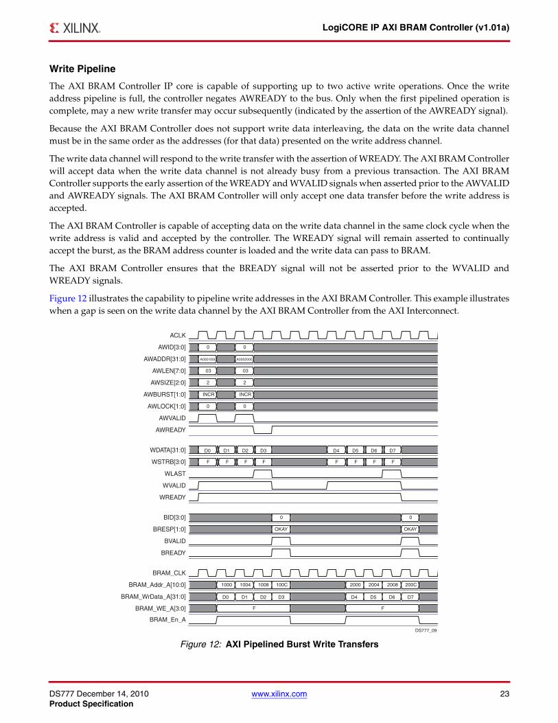
Write Pipeline
The AXI BRAM Controller IP core is capable of supporting up to two active write operations. Once the writeaddress pipeline is full, the controller negates AWREADY to the bus. Only when the first pipelined operation iscomplete, may a new write transfer may occur subsequently (indicated by the assertion of the AWREADY signal).
Because the AXI BRAM Controller does not support write data interleaving, the data on the write data channelmust be in the same order as the addresses (for that data) presented on the write address channel.
The write data channel will respond to the write transfer with the assertion of WREADY. The AXI BRAM Controllerwill accept data when the write data channel is not already busy from a previous transaction. The AXI BRAMController supports the early assertion of the WREADY and WVALID signals when asserted prior to the AWVALIDand AWREADY signals. The AXI BRAM Controller will only accept one data transfer before the write address isaccepted.
The AXI BRAM Controller is capable of accepting data on the write data channel in the same clock cycle when thewrite address is valid and accepted by the controller. The WREADY signal will remain asserted to continuallyaccept the burst, as the BRAM address counter is loaded and the write data can pass to BRAM.
The AXI BRAM Controller ensures that the BREADY signal will not be asserted prior to the WVALID andWREADY signals.
Figure 12 illustrates the capability to pipeline write addresses in the AXI BRAM Controller. This example illustrateswhen a gap is seen on the write data channel by the AXI BRAM Controller from the AXI Interconnect.X-Ref Target - Figure 12
Figure 12: AXI Pipelined Burst Write Transfers
ACLK
AWID[3:0]
AWADDR[31:0]
AWLEN[7:0]
AWSIZE[2:0]
AWBURST[1:0]
AWLOCK[1:0]
AWVALID
AWREADY
WDATA[31:0]
WSTRB[3:0]
WLAST
WVALID
WREADY
BID[3:0]
BRESP[1:0]
BVALID
BREADY
BRAM_CLK
BRAM_Addr_A[10:0]
BRAM_WrData_A[31:0]
BRAM_WE_A[3:0]
BRAM_En_A
0 0
A0001000 A0002000
03 03
2 2
INCR INCR
0 0
D0 D1 D2 D3 D4 D5 D6 D7
F F F F F F F F
0 0
OKAY OKAY
1000 1004 1008 100C 2000 2004 2008 200C
F F
D0 D1 D2 D3 D4 D5 D6 D7
DS777_09

DS777 December 14, 2010 www.xilinx.com 24Product Specification
LogiCORE IP AXI BRAM Controller (v1.01a)
The AXI BRAM Controller can support back-to-back write burst operations if it supplied with a continuous datastream from the AXI Interconnect. In this case, there are no idle clock cycles on the BRAM interface between the twopipelined write burst operations. Figure 13 illustrates the timing for back-to-back pipelined write bursts of fourdata beats.
100% BRAM interface utilization can be achieved on the write port under the following conditions:
• No single write bursts.
• Write burst must be greater than two data beats.
• Write burst operation must be an INCR or WRAP burst type.X-Ref Target - Figure 13
Figure 13: AXI Back-to-Back Write Burst Timing
ACLK
AWID[3:0]
AWADDR[31:0]
AWLEN[7:0]
AWSIZE[2:0]
AWBURST[1:0]
AWLOCK[1:0]
AWVALID
AWREADY
WDATA[31:0]
WSTRB[3:0]
WLAST
WVALID
WREADY
BID[3:0]
BRESP[1:0]
BVALID
BREADY
BRAM_CLK
BRAM_Addr_A[10:0]
BRAM_WrData_A[31:0]
BRAM_WE_A[3:0]
BRAM_En_A
0 0
A0001000 A0002000
03 03
2 2
INCR INCR
0 0
D0 D1 D2 D3 D4 D5 D6 D7
F F F F F F F F
0 0
OKAY OKAY
1000 1004 1008 100C 2000 2004 2008 200C
F F F F F F F F
D0 D1 D2 D3 D4 D5 D6 D7
DS777_13
DS777 December 14, 2010 www.xilinx.com 25Product Specification
LogiCORE IP AXI BRAM Controller (v1.01a)
Delayed Write Address
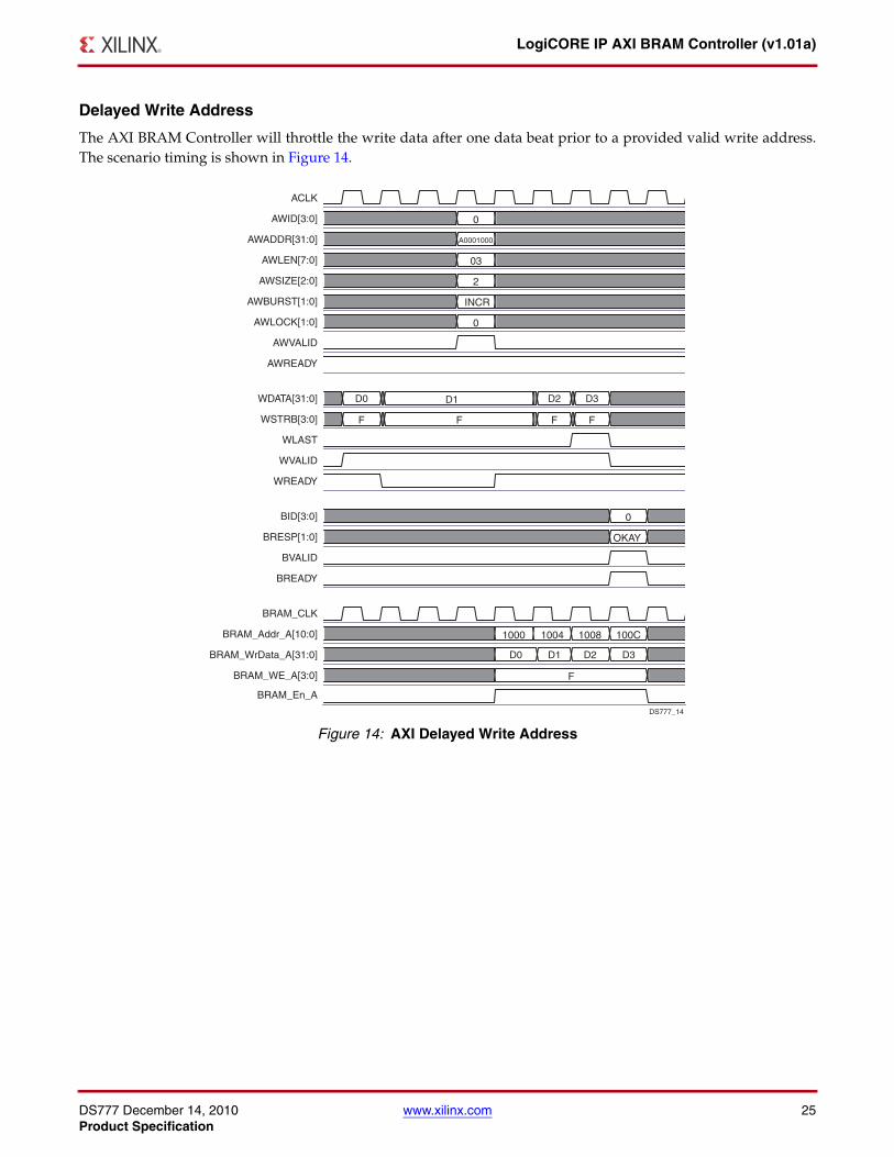
The AXI BRAM Controller will throttle the write data after one data beat prior to a provided valid write address.The scenario timing is shown in Figure 14.X-Ref Target - Figure 14
Figure 14: AXI Delayed Write Address
ACLK
AWID[3:0]
AWADDR[31:0]
AWLEN[7:0]
AWSIZE[2:0]
AWBURST[1:0]
AWLOCK[1:0]
AWVALID
AWREADY
WDATA[31:0]
WSTRB[3:0]
WLAST
WVALID
WREADY
BID[3:0]
BRESP[1:0]
BVALID
BREADY
BRAM_CLK
BRAM_Addr_A[10:0]
BRAM_WrData_A[31:0]
BRAM_WE_A[3:0]
BRAM_En_A
0
A0001000
03
2
INCR
0
D0 D1 D2 D3
F F F F
0
OKAY
1000 1004 1008 100C
D0 D1 D2 D3
F
DS777_14

DS777 December 14, 2010 www.xilinx.com 26Product Specification
LogiCORE IP AXI BRAM Controller (v1.01a)
Read Bursting
Figure 15 illustrates the example timing for an AXI read burst with BRAM handled by the AXI BRAM Controller.The memory read burst starts at address 0x1000h of the BRAM, provided that C_S_AXI_BASEADDR = 0xA000 0000and that C_S_AXI_HIGHADDR allows more than 4 k of addressable memory. The AXI Read Address Channelinterface maintains the ARREADY signal asserted until the read address pipeline is full in the AXI BRAMController. On the AXI Read Data Channel, the AXI BRAM Controller supports the AXI master/Interconnect torespond to the RVALID assertion with a same clock cycle assertion of RREADY. If the requesting AXImaster/Interconnect throttles upon accepting the read burst data (by negating RREADY), the AXI BRAMController can manage this condition and holds the data pipeline until the RREADY signal is asserted.
Read Throttling
The AXI BRAM Controller must support read throttling. During a read operation, the AXI BRAM will issue readcommands to the BRAM, but can only read ahead two addresses (the amount of BRAM read data beats supportedin the AXI BRAM Controller read data skid buffer pipeline). The requesting AXI master is not required to captureall the data immediately, but may throttle and assert only the RREADY signal when data can be accepted. The AXIBRAM Controller must halt the read operation and hold the existing read data when the requesting master negatesRREADY. Figure 16 illustrates this behavior and corresponding BRAM port operation. The two stage read datapipeline ensures that all outputs to BRAM and outputs to the AXI read data channel are registered.
X-Ref Target - Figure 15
Figure 15: AXI Read Burst Diagram
ACLK
ARID[3:0]
ARADDR[31:0]
ARLEN[7:0]
ARSIZE[2:0]
ARBURST[1:0]
ARLOCK[1:0]
ARVALID
ARREADY
RID[3:0]
RDATA[31:0]
RRESP[1:0]
RLAST
RVALID
RREADY
BRAM_Clk
BRAM_Addr_B[10:0]
BRAM_RdData_B[31:0]
BRAM_En_B
0
A0001000
03
2
INCR
0
0
D0 D1 D2 D3
OKAY
1000 1004 1008 100C
D0 D1 D2 D3
DS777_15
DS777 December 14, 2010 www.xilinx.com 27Product Specification
LogiCORE IP AXI BRAM Controller (v1.01a)
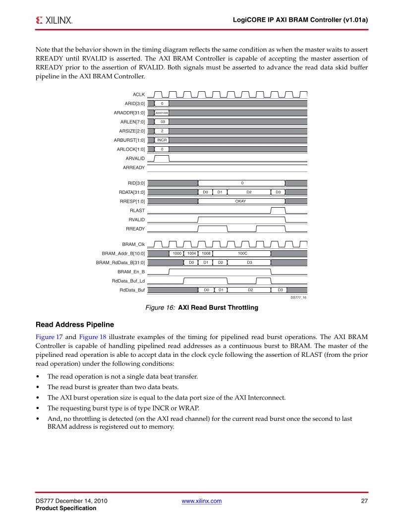
Note that the behavior shown in the timing diagram reflects the same condition as when the master waits to assertRREADY until RVALID is asserted. The AXI BRAM Controller is capable of accepting the master assertion ofRREADY prior to the assertion of RVALID. Both signals must be asserted to advance the read data skid bufferpipeline in the AXI BRAM Controller.
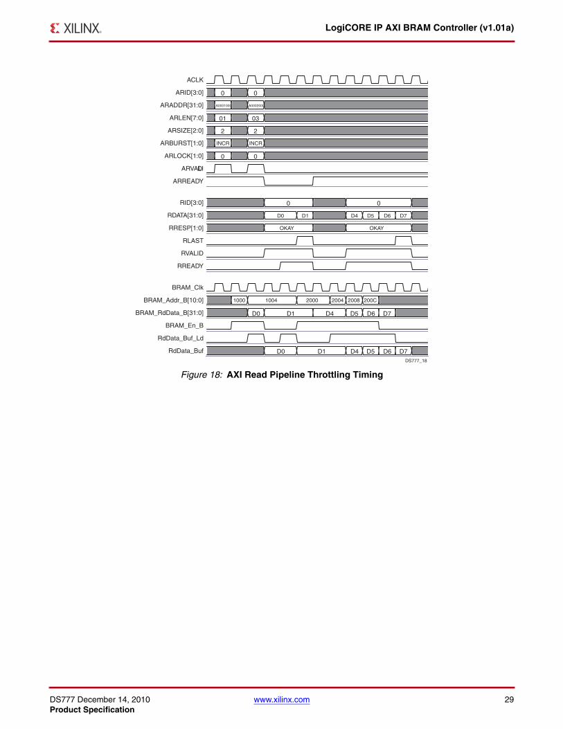
Read Address Pipeline
Figure 17 and Figure 18 illustrate examples of the timing for pipelined read burst operations. The AXI BRAMController is capable of handling pipelined read addresses as a continuous burst to BRAM. The master of thepipelined read operation is able to accept data in the clock cycle following the assertion of RLAST (from the priorread operation) under the following conditions:
• The read operation is not a single data beat transfer.
• The read burst is greater than two data beats.
• The AXI burst operation size is equal to the data port size of the AXI Interconnect.
• The requesting burst type is of type INCR or WRAP.
• And, no throttling is detected (on the AXI read channel) for the current read burst once the second to last BRAM address is registered out to memory.
X-Ref Target - Figure 16
Figure 16: AXI Read Burst Throttling
ACLK
ARID[3:0]
ARADDR[31:0]
ARLEN[7:0]
ARSIZE[2:0]
ARBURST[1:0]
ARLOCK[1:0]
ARVALID
ARREADY
RID[3:0]
RDATA[31:0]
RRESP[1:0]
RLAST
RVALID
RREADY
BRAM_Clk
BRAM_Addr_B[10:0]
BRAM_RdData_B[31:0]
BRAM_En_B
RdData_Buf_Ld
RdData_Buf
0
A0001000
03
2
INCR
0
0
D0 D1 D2 D3
OKAY
1000 1004 1008 100C
D0 D1 D2 D3
D0 D1 D2 D3
DS777_16

DS777 December 14, 2010 www.xilinx.com 28Product Specification
LogiCORE IP AXI BRAM Controller (v1.01a)
If any of the previously cited conditions exist on the pipelined read operations, the master must wait until RVALIDis re-asserted to begin reading data for the subsequent burst. The expected delay is two AXI clock cycles untilRVALID will be asserted after the prior RLAST (when any of these above conditions exist). Figure 18 illustrates thetiming for this scenario.
Figure 17 illustrates the ability of the AXI BRAM Controller to accept pipelined read request addresses andmaintain 100% bus utilization to the BRAM. The data burst must be greater than two data beats to reach amaximum 100% data throughput from the BRAM with no idle clock cycles on the AXI read data channel. Therequesting burst type must be INCR or WRAP type and the requesting read burst size must be equal to the size ofthe AXI Interconnect read data port (no narrow burst type transactions) to achieve 100% bus utilization onpipelined read bursts.
Utilization of the read data skid buffer illustrates the master’s capability to throttle on accepting read data. Theresulting BRAM transaction timing is shown in Figure 18.X-Ref Target - Figure 17
Figure 17: AXI 100% Bus Utilization on Pipelined Read Bursts
ACLK
ARID[3:0]
ARADDR[31:0]
ARLEN[7:0]
ARSIZE[2:0]
ARBURST[1:0]
ARLOCK[1:0]
ARVALID
ARREADY
RID[3:0]
RDATA[31:0]
RRESP[1:0]
RLAST
RVALID
RREADY
BRAM_Clk
BRAM_Addr_B[10:0]
BRAM_RdData_B[31:0]
BRAM_En_B
RdData_Buf_Ld
RdData_Buf
0 0
A0001000 A0002000
03 03
2 2
INCR INCR
0 0
0
D0 D1 D2 D3 D4 D5 D6 D7
OKAY
1000 1004 1008 100C 2000 2004 2008 200C
D0 D1 D2 D3 D4 D5 D6 D7
D0 D1 D2 D3 D4 D5 D6 D7
DS777_17
DS777 December 14, 2010 www.xilinx.com 29Product Specification
LogiCORE IP AXI BRAM Controller (v1.01a)
X-Ref Target - Figure 18
Figure 18: AXI Read Pipeline Throttling Timing
ACLK
ARID[3:0]
ARADDR[31:0]
ARLEN[7:0]
ARSIZE[2:0]
ARBURST[1:0]
ARLOCK[1:0]
ARVALID
ARREADY
RID[3:0]
RDATA[31:0]
RRESP[1:0]
RLAST
RVALID
RREADY
BRAM_Clk
BRAM_Addr_B[10:0]
BRAM_RdData_B[31:0]
BRAM_En_B
RdData_Buf_Ld
RdData_Buf
0 0
A0001000 A0002000
01 03
2 2
INCR INCR
0 0
0 0
OKAY OKAY
1000 1004 2000 2004 2008 200C
D0 D1 D4 D5 D6 D7
D0 D1 D4 D5 D6 D7
D0 D1 D4 D5 D6 D7
DS777_18

DS777 December 14, 2010 www.xilinx.com 30Product Specification
LogiCORE IP AXI BRAM Controller (v1.01a)
Cacheline Reads
Figure 19 illustrates the timing on AXI WRAP or cacheline burst transactions. The address generated to the BRAMstarts at the target word and wraps around once the address boundary is reached.
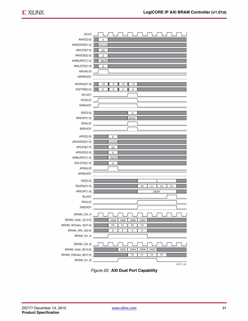
Dual Port Capability
Isolating the write and read ports to BRAM with each write and read channel interface on the AXI bus, both BRAMports can be utilized simultaneously. Figure 20 illustrates this condition to provide no arbitration on the write orread channels dependency on the other.
X-Ref Target - Figure 19
Figure 19: AXI Cacheline Read
ACLK
ARID[3:0]
ARADDR[31:0]
ARLEN[7:0]
ARSIZE[2:0]
ARBURST[1:0]
ARLOCK[1:0]
ARVALID
ARREADY
RID[3:0]
RDATA[31:0]
RRESP[1:0]
RLAST
RVALID
RREADY
BRAM_Clk
BRAM_Addr_B[10:0]
BRAM_RdData_B[31:0]
BRAM_En_B
0
A0001004
03
2
WRAP
0
0
D1 D2 D3 D0
OKAY
1004 1008 100C 1000
D1 D2 D3 D0
DS777_19
DS777 December 14, 2010 www.xilinx.com 31Product Specification
LogiCORE IP AXI BRAM Controller (v1.01a)
X-Ref Target - Figure 20
Figure 20: AXI Dual Port Capability
ACLK
AWID[3:0]
AWADDR[31:0]
AWLEN[7:0]
AWSIZE[2:0]
AWBURST[1:0]
AWLOCK[1:0]
AWVALID
AWREADY
WDATA[31:0]
WSTRB[3:0]
WLAST
WVALID
WREADY
BID[3:0]
BRESP[1:0]
BVALID
BREADY
ARID[3:0]
ARADDR[31:0]
ARLEN[7:0]
ARSIZE[2:0]
ARBURST[1:0]
ARLOCK[1:0]
ARVALID
ARREADY
RID[3:0]
RDATA[31:0]
RRESP[1:0]
RLAST
RVALID
RREADY
BRAM_Clk_A
BRAM_Addr_A[10:0]
BRAM_WrData_A[31:0]
BRAM_WE_A[3:0]
BRAM_En_A
BRAM_Addr_B[10:0]
BRAM_RdData_B[31:0]
BRAM_En_B
0
A0001000
03
2
INCR
0
F F F F
0
OKAY
0
A0002000
03
2
INCR
0
0
OKAY
1000 1004 1008 100C
F F F F
D0 D1 D2 D3
D0 D1 D2 D3
D0 D1 D2 D3
2000 2004 2008 200C
D0 D1 D2 D3
BRAM_Clk_B
DS777_20

DS777 December 14, 2010 www.xilinx.com 32Product Specification
LogiCORE IP AXI BRAM Controller (v1.01a)
Design Implementation
Target Technology
The intended target technology for this design is Virtex-6 and Spartan-6 Xilinx FPGAs.
EDK Implementation
The following parameters can be set in the MHS file when the AXI BRAM Controller is integrated into an EDK AXIsystem:
PARAMETER C_INTERCONNECT_S_AXI_AR_REGISTER = 1PARAMETER C_INTERCONNECT_S_AXI_AW_REGISTER = 1PARAMETER C_INTERCONNECT_S_AXI_B_REGISTER = 1PARAMETER C_INTERCONNECT_S_AXI_R_REGISTER = 1PARAMETER C_INTERCONNECT_S_AXI_W_REGISTER = 1
Setting these parameters enables registers on the AXI channels in the AXI Interconnect IP core.
For additional timing improvements in AXI4 systems with stringent FMAX requirements, the AXI BRAM IP core canbe optimized when there are no AXI masters in the system that support narrow transactions to the BRAM. Settingthe design parameter, C_S_AXI_SUPPORTS_NARROW_BURST = 0 in the MHS of the EDK system will improvetiming paths. Logic to support the narrow transfers in the write and read channels of the AXI BRAM IP areoptimized away by XST during synthesis of the core. The EDK tools set C_S_AXI_SUPPORTS_NARROW_BURSTto 0 automatically, if it detects that all connected masters have declared that they do not generate narrow bursttransactions.
Device Utilization and Performance Benchmarks
Core Performance
Because the AXI BRAM Controller IP core will be used with other design modules in the FPGA, the utilization andtiming numbers reported in this section are estimates only. When the AXI BRAM Controller core is combined withother designs in the system, the utilization of FPGA resources and timing of the AXI BRAM Controller IP core willvary from the results reported here.

DS777 December 14, 2010 www.xilinx.com 33Product Specification
LogiCORE IP AXI BRAM Controller (v1.01a)
Table 9 shows the AXI BRAM Controller resource utilization for various parameter combinations measured withthe Virtex-6 FPGA (xc6vlx240t) FPGA as the target device.
The maximum (-1 speed grade) clock frequency on the AXI BRAM Controller IP core with an AXI4 IF in the Virtex-6FPGA architecture (-1 speed grade) is 180 MHz.
For an AXI4-Lite system, the maximum target clock frequency in a Virtex-6 FPGA is 135 MHz.
Table 9: Performance and Resource Utilization Benchmarks on the Virtex-6 FPGA
Parameter Values (Other parameters at default values) Device Resources (1)
C_S
_AX
I_P
RO
TOC
OL
C_B
RA
M_D
WID
TH
C_S
_AX
I_S
UP
PO
RT
S_N
AR
RO
W_B
UR
ST
C_S
ING
LE_P
OR
T_B
RA
M
Slic
es
Slic
e R
egis
ters
LUT
s
AXI4 32 0 N/A 187 312 362
AXI4 32 1 N/A 192 329 381
AXI4 64 0 N/A 172 408 375
AXI4 64 1 N/A 207 430 414
AXI4 128 0 N/A 215 595 401
AXI4 128 1 N/A 245 633 454
AXI4LITE 32 N/A 0 5 5 11
AXI4LITE 32 N/A 1 6 5 12
Notes: 1. The number of block RAMs used depends on parameter settings for C_S_AXI_BASEADDR, C_S_AXI_HIGHADDR, and
C_S_AXI_DATA_WIDTH. Please refer to Table 5 for more details.

DS777 December 14, 2010 www.xilinx.com 34Product Specification
LogiCORE IP AXI BRAM Controller (v1.01a)
Table 10 shows the AXI BRAM Controller resource utilization for various parameter combinations measured withthe Spartan-6 FPGA (xc6slx45t) FPGA as the target device.
The maximum target clock frequency on the AXI BRAM Controller IP core with an AXI4 IF in the Spartan-6 FPGAarchitecture (-2 speed grade) is 120 MHz.
For an AXI4-Lite system, the maximum target clock frequency in a Virtex-6 FPGA is 90 MHz.
Table 10: Performance and Resource Utilization Benchmarks on the Spartan-6 FPGA
Parameter Values (Other parameters at default values) Device Resources (1)
C_S
_AX
I_P
RO
TOC
OL
C_B
RA
M_D
WID
TH
C_S
_AX
I_S
UP
PO
RT
S_N
AR
RO
W_B
UR
ST
C_S
ING
LE_P
OR
T_B
RA
M
Slic
es
Slic
e R
egis
ters
LUT
s
AXI4 32 0 N/A 160 284 389
AXI4 32 1 N/A 201 307 383
AXI4 64 0 N/A 181 378 362
AXI4 64 1 N/A 224 409 425
AXI4 128 0 N/A 262 597 424
AXI4 128 1 N/A 319 635 480
AXI4LITE 32 N/A 0 6 5 11
AXI4LITE 32 N/A 1 6 5 12
Notes: 1. The number of block RAMs used depends on parameter settings for C_S_AXI_BASEADDR, C_S_AXI_HIGHADDR, and
C_S_AXI_DATA_WIDTH. Please refer to Table 6 for more details.
DS777 December 14, 2010 www.xilinx.com 35Product Specification
LogiCORE IP AXI BRAM Controller (v1.01a)
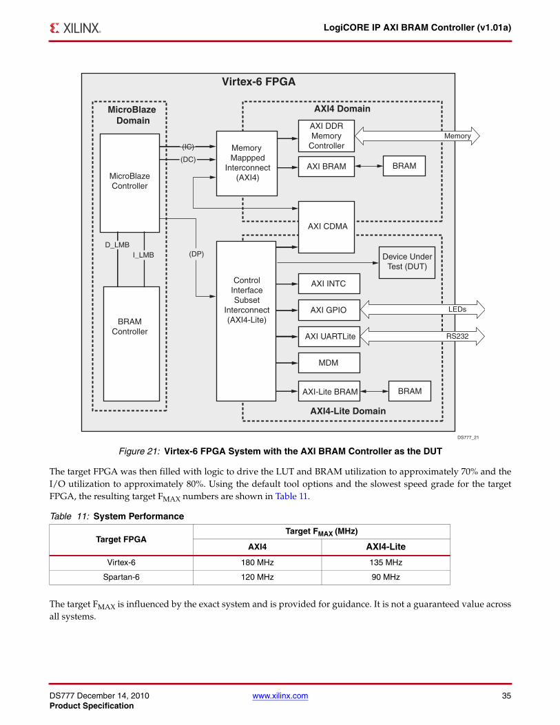
The target FPGA was then filled with logic to drive the LUT and BRAM utilization to approximately 70% and theI/O utilization to approximately 80%. Using the default tool options and the slowest speed grade for the targetFPGA, the resulting target FMAX numbers are shown in Table 11.
The target FMAX is influenced by the exact system and is provided for guidance. It is not a guaranteed value acrossall systems.
X-Ref Target - Figure 21
Figure 21: Virtex-6 FPGA System with the AXI BRAM Controller as the DUT
Table 11: System Performance
Target FPGATarget FMAX (MHz)
AXI4 AXI4-Lite
Virtex-6 180 MHz 135 MHz
Spartan-6 120 MHz 90 MHz
AXI4-Lite Domain
MicroBlazeController
AXI INTC
AXI GPIO
AXI UARTLite
AXI DDRMemory
Controller
MDM
MicroBlaze Domain
AXI4 Domain
BRAMController
D_LMBI_LMB
(IC)
AXI BRAM(DC)
Device UnderTest (DUT)
Memory
(DP)
DS777_21
LEDs
RS232
AXI CDMA
Virtex-6 FPGA
Memory Mappped
Interconnect(AXI4)
ControlInterfaceSubset
Interconnect(AXI4-Lite)
AXI-Lite BRAM BRAM
BRAM

DS777 December 14, 2010 www.xilinx.com 36Product Specification
LogiCORE IP AXI BRAM Controller (v1.01a)
Reference Documents1. AMBA® AXI Protocol Version: 2.0 Specification (ARM IHI 0022C)
2. DS768 AXI Interconnect IP Data Sheet
3. DS150 Virtex-6 Family Overview
4. DS160 Spartan-6 Family Overview
SupportXilinx provides technical support for this LogiCORE product when used as described in the productdocumentation. Xilinx cannot guarantee timing, functionality, or support of product if implemented in devices thatare not defined in the documentation, if customized beyond that allowed in the product documentation, or ifchanges are made to any section of the design labeled DO NOT MODIFY.
Ordering InformationThis Xilinx LogiCORE IP module is provided at no additional cost with the Xilinx ISE® Design Suite EmbeddedEdition software under the terms of the Xilinx End User License. The core is generated using the Xilinx ISEEmbedded Edition software (EDK).
Information about this and other Xilinx LogiCORE IP modules is available at the Xilinx Intellectual Property page.For information on pricing and availability of other Xilinx LogiCORE modules and software, please contact yourlocal Xilinx sales representative.
Revision History
Notice of DisclaimerXilinx is providing this product documentation, hereinafter “Information,” to you “AS IS” with no warranty of any kind, expressor implied. Xilinx makes no representation that the Information, or any particular implementation thereof, is free from anyclaims of infringement. You are responsible for obtaining any rights you may require for any implementation based on theInformation. All specifications are subject to change without notice. XILINX EXPRESSLY DISCLAIMS ANY WARRANTYWHATSOEVER WITH RESPECT TO THE ADEQUACY OF THE INFORMATION OR ANY IMPLEMENTATION BASEDTHEREON, INCLUDING BUT NOT LIMITED TO ANY WARRANTIES OR REPRESENTATIONS THAT THISIMPLEMENTATION IS FREE FROM CLAIMS OF INFRINGEMENT AND ANY IMPLIED WARRANTIES OFMERCHANTABILITY OR FITNESS FOR A PARTICULAR PURPOSE. Except as stated herein, none of the Information may becopied, reproduced, distributed, republished, downloaded, displayed, posted, or transmitted in any form or by any meansincluding, but not limited to, electronic, mechanical, photocopying, recording, or otherwise, without the prior written consent ofXilinx.
Date Version Description of Revisions
9/21/10 1.0 Xilinx initial release.
12/14/10 1.1
Updated for 12.4 release; new version of HDL, v1.01a; includes support for AXI-4 Lite interface connections with a reduced footprint optimization. In an AXI-4 Lite mode, the BRAM port can be configured for single or dual port access. Also, C_S_AXI_BASEADDR and C_S_AXI_HIGHADDR have been moved as non HDL parameters.