logic design 2 - book spar
TRANSCRIPT
USN
Time: 3 hrs.
10ES33
N4ax. Marks:100
its input and(06 Marks)
Third Semester B.E. Degree Examination, Dec.20l4/Jan.20l5Logic Design
a.
b
o
O
c-
CtaC3
-oO
a)
t:
;.=
^l
-O
3>t'-
'ad
OD
50r
=.d:
'J-
!'u
.-Fr-C-oj
a=:+!o
>a'+-^o'E=O=--o
U<
a)
z
o.
Note: Answer I-IVE full questions, selectingatlesst TWO questions frorn esch part.
PART * Aa. Design a combinational circuit which takes two, 2 bit binary numbels as
generates an output equal to l, when the sum of the two numbers is odd.b. Convert the given Boolean function into :
i) R = f ta.b.c; = (; + bXb +i)minterm canonical lorm
ii) P : f(x,y,z) : x + xz(Y+ z) maxterm canonical form.c. Distinguish prime implicant and essential prime implicant. Determine
given function N : (a, b. c. d): Tr(0, 1,4,5,8, 9, 11) + d(2, l0) .
function and implement using logic gates.
Simplify the given Boolean function using Quine - Mccluskey method :
Y : f(a, b, c, d) : t(0, 1,2, 6,7,9, 10, 12) + d(3. 5). Verifu the result using t --ap.,t0 Marks)
Find the minimal sum and minimal procluct firr the giren Boolean function, using MEVtechnique : Solve byusing 3-variable map and 2 - variable map y: f(a, b, c, d) :2(2,3,4.5, 13, 1,5) + d(9, g, 10, 11). (10 Marks)
3 a. Distinguish between a decoder and an encoder. Implenrent full adder using IC 74138.(08 Marks)
b. Irnplement 3 - bit binary to gray sode convelsion by using IC 74139. (06 Nttarks)c. Design a priority encoder for a system with a 3 inputs, the middle bit with highest priority
encoding to 10, the MSB with next priority encoding to 11, while the LSB r.vith least priorityencoding to 01. (06 Marks)
4 a. Realize the following Boolean function : P : (w, x. y, z): t(0, 1, 5, 6, 7, 10,15) using :
(06 Marks)
PI and EPI fbr the
Simplify the given(08 Marks)
(10 N{arks)(10 Marks)
(06 Marks)shift register.
(06 Marks)positive edge
(08 Nlarks)
PART _ B
5 a. Explain the working of a master -slave SR flip-t1op with the help of a logic diagram,function table, logic symbol and timing diagram. (10 Nlarks)
b. With a neat logic diagram, explain the working of positrve edge triggered D flip-flop.(10 N{arks)
i) 16to 1 MUX ii)8 : I MUX iii)4 : I MUX.b. With a neat logic diagram, explain carry look ahead adder.
6 a. Obtain the characteristic equation for D and T flip-flop.b. With a neat logic diagram, explain the operation of 4-bit SISO unidirectional
c. Explain the wolking of four-bit binary ripple up counter, configured usingtriggered flip-flop. Also draw the timing diagram.
l of 2
www.bookspar.com | VTU NOTES | QUESTION PAPERS | NEWS | VTU RESULTS | FORUM | VTU BOOKSPAR APP
www.bookspar.com | VTU NOTES | QUESTION PAPERS | NEWS | VTU RESULTS | FORUM | VTU BOOKSPAR APP
la.
b.
c.
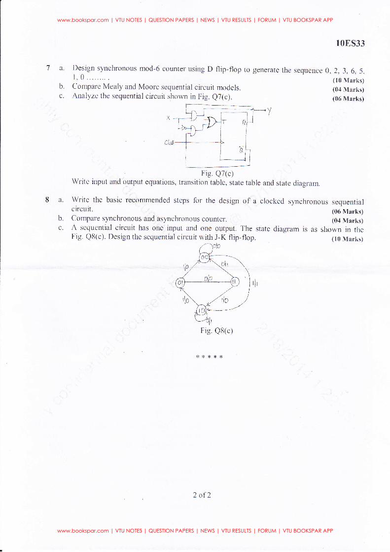
Design synchronous mod-6 counter using D flip-flop to1,0..Compare Mealy and Moore sequential circuit models.Analyze the sequential circuit shown in Fig. e7(c).
l0ES33
generate the sequence 0,2, 3, 6. 5,
(10 Marks)(04 Marks)(06 Marks)
write input and outpur equations, ,ru,rrfti*9,'u3;:?*, table and stare diag'a*
a. Write the basic recommended steps for the design of a clocked synchronous sequentialcircuit. (06 Marks)
b. compare synchronous and asynchronous counter. (04 Marks)c. A sequential circuit has one input and one output. The state diagram is as shown in the
Fig. Q8(c). Design rhe sequenrial circuit with J-K flip-flop. (10 Marks)
tlo,,/ o\r
ol
tio t/o
Fig. Q8(c)
tlr
*****
2 of 2
www.bookspar.com | VTU NOTES | QUESTION PAPERS | NEWS | VTU RESULTS | FORUM | VTU BOOKSPAR APP
www.bookspar.com | VTU NOTES | QUESTION PAPERS | NEWS | VTU RESULTS | FORUM | VTU BOOKSPAR APP