lmos evolution
TRANSCRIPT

6.720J/3.43J - Integrated Microelectronic Devices - Spring 2007 Lecture 33-1
Lecture 33 - The ”Short”Metal-Oxide-Semiconductor Field-Effect
Transistor (cont.)
April 30, 2007
Contents:
1. MOSFET scaling (cont.)
2. Evolution of MOSFET design
Cite as: Jesús del Alamo, course materials for 6.720J Integrated Microelectronic Devices, Spring 2007.MIT OpenCourseWare (http://ocw.mit.edu/), Massachusetts Institute of Technology. Downloaded on [DD Month YYYY].
6.720J/3.43J - Integrated Microelectronic Devices - Spring 2007 Lecture 33-2
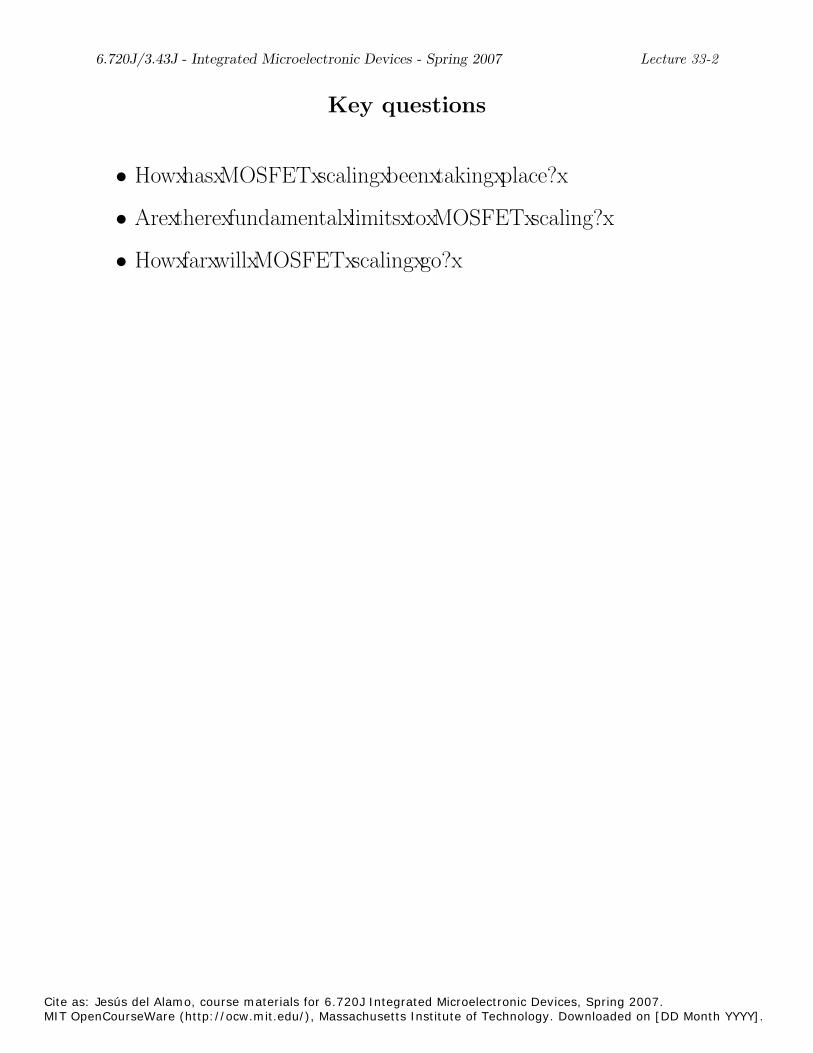
Key questions
• How has MOSFET scaling been taking place?
• Are there fundamental limits to MOSFET scaling?
• How far will MOSFET scaling go?
Cite as: Jesús del Alamo, course materials for 6.720J Integrated Microelectronic Devices, Spring 2007.MIT OpenCourseWare (http://ocw.mit.edu/), Massachusetts Institute of Technology. Downloaded on [DD Month YYYY].

6.720J/3.43J - Integrated Microelectronic Devices - Spring 2007 Lecture 33-3
1. Scaling (cont.)
Scaling goal: extract maximum performance from each generation (maximize Ion), for a given amount of:
• short-channel effects (DIBL), and
off-current •
To preserve electrostatic integrity, scaling has proceeded in a har
monious way: L ( ), W ( ), xox ( ), NA ( ), xj ( ), and VDD ( ).↓ ↓ ↓ ↑ ↓ ↓
Cite as: Jesús del Alamo, course materials for 6.720J Integrated Microelectronic Devices, Spring 2007.MIT OpenCourseWare (http://ocw.mit.edu/), Massachusetts Institute of Technology. Downloaded on [DD Month YYYY].

Illustration
6.720J/3.43J - Integrated Microelectronic Devices - Spring 2007 Lecture 33-4
of key trade-offs:
• Ion vs. Ioff
1E-08
1E-07
1E-06
1E-05
1E-04
1E-03
1E-02
1E-01
I off
(µµA
/ µµm
)
MIT SSR III CMOS Technology
Vdd=2 V
0 200 400 600 800
Ion (µµA/µµm)
Cite as: Jesús del Alamo, course materials for 6.720J Integrated Microelectronic Devices, Spring 2007.MIT OpenCourseWare (http://ocw.mit.edu/), Massachusetts Institute of Technology. Downloaded on [DD Month YYYY].

6.720J/3.43J - Integrated Microelectronic Devices - Spring 2007 Lecture 33-5
• Ion vs. DIBL
Cite as: Jesús del Alamo, course materials for 6.720J Integrated Microelectronic Devices, Spring 2007.MIT OpenCourseWare (http://ocw.mit.edu/), Massachusetts Institute of Technology. Downloaded on [DD Month YYYY].

6.720J/3.43J - Integrated Microelectronic Devices - Spring 2007 Lecture 33-6
� Limits to scaling
The New York Times (Oct. 9, 1999)
Cite as: Jesús del Alamo, course materials for 6.720J Integrated Microelectronic Devices, Spring 2007.MIT OpenCourseWare (http://ocw.mit.edu/), Massachusetts Institute of Technology. Downloaded on [DD Month YYYY].
Text removed due to copyright restrictions.Markoff, John. "Chip Progress Forecast to Hit a Big Barrier."
The New York Times (October 9, 1999).
6.720J/3.43J - Integrated Microelectronic Devices - Spring 2007 Lecture 33-7
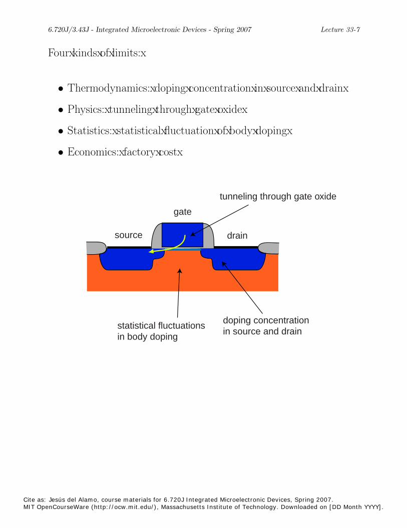
Four kinds of limits:
• Thermodynamics: doping concentration in source and drain
• Physics: tunneling through gate oxide
• Statistics: statistical fluctuation of body doping
• Economics: factory cost
tunneling through gate oxide
in source and drain in body doping
source
gate
drain
doping concentration � statistical fluctuations �
Cite as: Jesús del Alamo, course materials for 6.720J Integrated Microelectronic Devices, Spring 2007.MIT OpenCourseWare (http://ocw.mit.edu/), Massachusetts Institute of Technology. Downloaded on [DD Month YYYY].
6.720J/3.43J - Integrated Microelectronic Devices - Spring 2007 Lecture 33-8
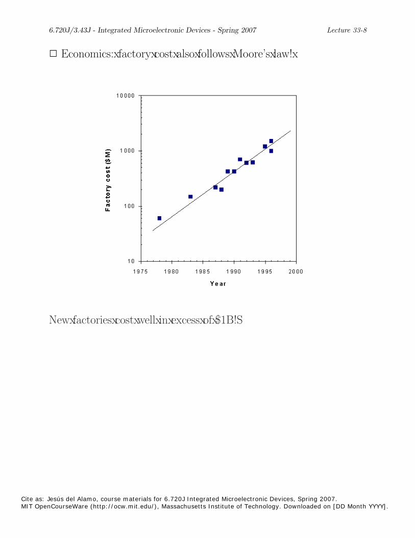
� Economics: factory cost also follows Moore’s law!
New factories cost well in excess of $1B!
Cite as: Jesús del Alamo, course materials for 6.720J Integrated Microelectronic Devices, Spring 2007.MIT OpenCourseWare (http://ocw.mit.edu/), Massachusetts Institute of Technology. Downloaded on [DD Month YYYY].

6.720J/3.43J - Integrated Microelectronic Devices - Spring 2007 Lecture 33-9
� Physics: tunneling through gate oxide (most severe limit)
• Oxide’s thickness limit when:
Igate � Ioff @ VDD � 1 V, Toper(� 100oC)
• Translates to limiting gate current:
Igate(25oC) � 100 pA
• Limiting gate current density:
Ioff (100oC)Ioff (25oC)
A � 0.1 µm×0.1 µm = 10−10 cm 2 ⇒ Jgate(25oC) � 1 A/cm2
• Limiting xox � 1.6 nm ⇒ L ∼ 35 − 50 nm
• Solution: high-dielectric constant gate insulator
Cite as: Jesús del Alamo, course materials for 6.720J Integrated Microelectronic Devices, Spring 2007.MIT OpenCourseWare (http://ocw.mit.edu/), Massachusetts Institute of Technology. Downloaded on [DD Month YYYY].
Figure 13 on p. 491 in: Taur, Y., et al. "CMOS Scaling into the Nanometer Regime."Proceedings of the IEEE 85, no. 4 (1997): 486-504. © 1997 IEEE.
6.720J/3.43J - Integrated Microelectronic Devices - Spring 2007 Lecture 33-10
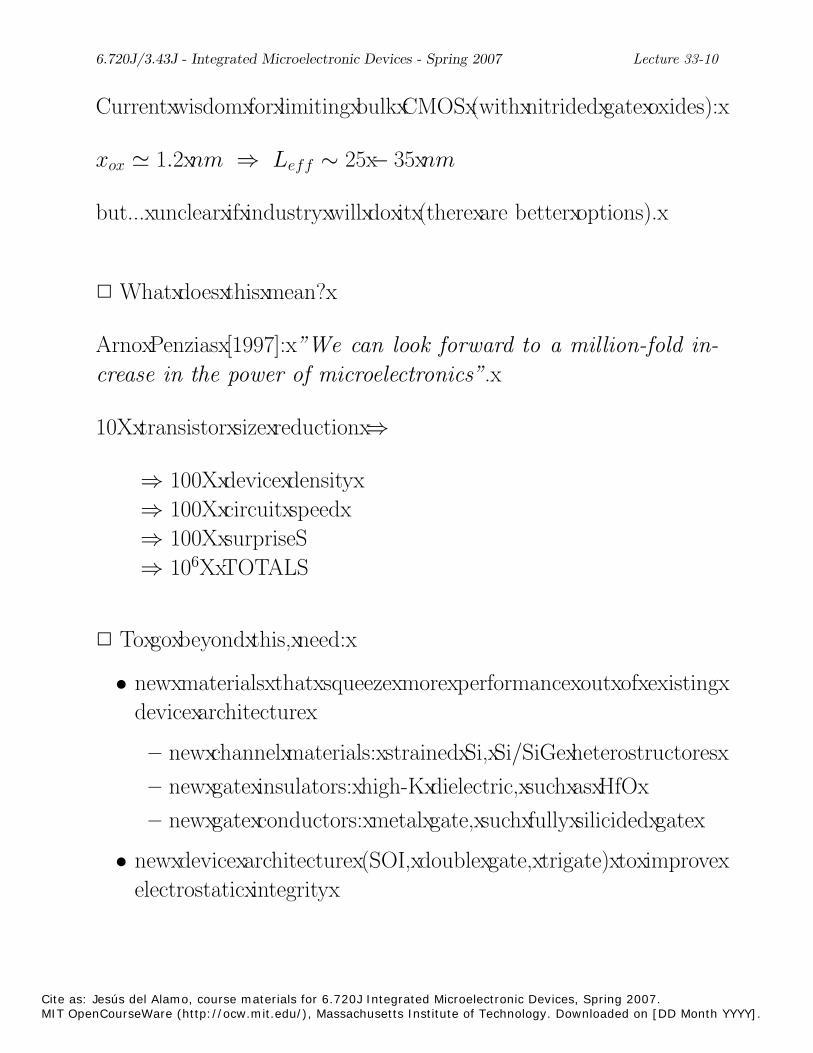
Current wisdom for limiting bulk CMOS (with nitrided gate oxides):
xox � 1.2 nm Leff ∼ 25 − 35 nm⇒
but... unclear if industry will do it (there are better options).
� What does this mean?
Arno Penzias [1997]: ”We can look forward to a million-fold in
crease in the power of microelectronics”.
10X transistor size reduction ⇒
⇒ 100X device density
⇒ 100X circuit speed
⇒ 100X surprise
106X TOTAL⇒
� To go beyond this, need:
• new materials that squeeze more performance out of existing
device architecture
– new channel materials: strained Si, Si/SiGe heterostructores
– new gate insulators: high-K dielectric, such as HfO
– new gate conductors: metal gate, such fully silicided gate
• new device architecture (SOI, double gate, trigate) to improve
electrostatic integrity
Cite as: Jesús del Alamo, course materials for 6.720J Integrated Microelectronic Devices, Spring 2007.MIT OpenCourseWare (http://ocw.mit.edu/), Massachusetts Institute of Technology. Downloaded on [DD Month YYYY].

6.720J/3.43J - Integrated Microelectronic Devices - Spring 2007 Lecture 33-11
2. Evolution of MOSFET design
• PMOS with metal gate:
Al gate
p+p+
n
circa∼early 70’s
L ∼ 20 µm
xox ∼ 1000 A
xj ∼ 3 µm
VDD = 12 V
Main point: Na+ contamination made NMOS devices to have too
negative a threshold voltage
Cite as: Jesús del Alamo, course materials for 6.720J Integrated Microelectronic Devices, Spring 2007.MIT OpenCourseWare (http://ocw.mit.edu/), Massachusetts Institute of Technology. Downloaded on [DD Month YYYY].

•
6.720J/3.43J - Integrated Microelectronic Devices - Spring 2007 Lecture 33-12
NMOS with metal gate:
Al gate
n+n+
p
circa∼1975
L ∼ 15 µm
xox ∼ 600 A
xj ∼ 2 µm
VDD = 12 V
Main point: with Na+ contamination under control, NMOS devices
became possible (higher performance).
Cite as: Jesús del Alamo, course materials for 6.720J Integrated Microelectronic Devices, Spring 2007.MIT OpenCourseWare (http://ocw.mit.edu/), Massachusetts Institute of Technology. Downloaded on [DD Month YYYY].

6.720J/3.43J - Integrated Microelectronic Devices - Spring 2007 Lecture 33-13
• CMOS with self-aligned polySi gate:
n+-polySi gate
n+n+
p
circa∼1980
L ∼ 2 µm
xox ∼ 400 A
xj ∼ 1 µm
VDD = 5 V
Main point: self-aligned process allows tighter overlap between gate
and n+ regions and results in lower parasitic capacitance.
Cite as: Jesús del Alamo, course materials for 6.720J Integrated Microelectronic Devices, Spring 2007.MIT OpenCourseWare (http://ocw.mit.edu/), Massachusetts Institute of Technology. Downloaded on [DD Month YYYY].

6.720J/3.43J - Integrated Microelectronic Devices - Spring 2007 Lecture 33-14
• Lightly-doped drain MOSFET (LDD-MOSFET):
n+ n n+
polycide gate: � deposited silicide (TaSi)�
n
�
n+-polySi
p
circa∼1985
L ∼ 0.75 µm
xox ∼ 200 A
xj ∼ 0.2 µm
VDD = 5 V
Main point: lightly-doped n-region on drain side reduces electric field
there and allows a high VDD to be used.
Cite as: Jesús del Alamo, course materials for 6.720J Integrated Microelectronic Devices, Spring 2007.MIT OpenCourseWare (http://ocw.mit.edu/), Massachusetts Institute of Technology. Downloaded on [DD Month YYYY].

6.720J/3.43J - Integrated Microelectronic Devices - Spring 2007 Lecture 33-15
• Salicide (self-aligned silicide) MOSFET:
self-aligned silicide (TaSi)�
n+-polySi
n+ n+nn
�
p
circa∼1989
L ∼ 0.4 µm
xox ∼ 125 A
xj ∼ 0.15 µm
VDD = 3.3 V
Main point: salicided gate, source and drain reduces all parasitic
resistances.
Cite as: Jesús del Alamo, course materials for 6.720J Integrated Microelectronic Devices, Spring 2007.MIT OpenCourseWare (http://ocw.mit.edu/), Massachusetts Institute of Technology. Downloaded on [DD Month YYYY].

6.720J/3.43J - Integrated Microelectronic Devices - Spring 2007 Lecture 33-16
• MOSFET with p-pocket or halo implants:
n+
p+p+
nn n+
p
circa∼1994
L ∼ 0.15 µm
xox ∼ 60 A
xj ∼ 0.08 µm
VDD = 2.5 V
Main point: p+ pockets control short-channel effects.
Cite as: Jesús del Alamo, course materials for 6.720J Integrated Microelectronic Devices, Spring 2007.MIT OpenCourseWare (http://ocw.mit.edu/), Massachusetts Institute of Technology. Downloaded on [DD Month YYYY].

6.720J/3.43J - Integrated Microelectronic Devices - Spring 2007 Lecture 33-17
• Sub-0.1 µm MOSFET:
n+ p+
p+ p+
nn n+
p
super-steep retrograde� body doping
circa∼late 90’s (manufacturing in early 00’s)
L < 0.1 µm
xox ∼ 30 A
xj ∼ 0.06 µm
VDD = 0.8 − 1.5 V
Main point: p+-super-steep retrograde body doping controls short-
channel effects while preserving high mobility.
Cite as: Jesús del Alamo, course materials for 6.720J Integrated Microelectronic Devices, Spring 2007.MIT OpenCourseWare (http://ocw.mit.edu/), Massachusetts Institute of Technology. Downloaded on [DD Month YYYY].

New
6.720J/3.43J - Integrated Microelectronic Devices - Spring 2007 Lecture 33-18
device architecture: Silicon-on-Insulator (SOI)
A number of issues associated with existence of buried oxide:
• reduced junction capacitance
• floating body: kink effect, extra drive (VBS > 0 during switch
ing)
increased thermal resistance •
Cite as: Jesús del Alamo, course materials for 6.720J Integrated Microelectronic Devices, Spring 2007.MIT OpenCourseWare (http://ocw.mit.edu/), Massachusetts Institute of Technology. Downloaded on [DD Month YYYY].
Figure 25.1.1 in: Shahidi, G.G., et al. "Partially-depleted SOI Technology for Digital Logic." International Solid-StateCircuits Conference, San Francisco, CA, Feb. 15-17, 1999. Digest of Technical Papers. New York, NY: Institute ofElectrical and Electronics Engineers, 1999, pp. 426-427. ISBN: 9780780351264. © 1999 IEEE.

6.720J/3.43J - Integrated Microelectronic Devices - Spring 2007 Lecture 33-19
New device architecture: Dual-gate MOSFET
Cite as: Jesús del Alamo, course materials for 6.720J Integrated Microelectronic Devices, Spring 2007.MIT OpenCourseWare (http://ocw.mit.edu/), Massachusetts Institute of Technology. Downloaded on [DD Month YYYY].
Figure 26 in Taur, Y., et al. "CMOS Scaling into the NanometerRegime." Proceedings of the IEEE 85, no. 4 (1997): 486-504.© 1997 IEEE.
Figure 29 in Taur, Y., et al. "CMOS Scaling into the NanometerRegime." Proceedings of the IEEE 85, no. 4 (1997): 486-504.© 1997 IEEE.

6.720J/3.43J - Integrated Microelectronic Devices - Spring 2007 Lecture 33-20
� Intel’s current (public) view of MOSFET scaling...
Cite as: Jesús del Alamo, course materials for 6.720J Integrated Microelectronic Devices, Spring 2007.MIT OpenCourseWare (http://ocw.mit.edu/), Massachusetts Institute of Technology. Downloaded on [DD Month YYYY].
Chau, R., et.al. "Advanced CMOS Transistors in the Nanotechnology Era for High-Performance, Low-Power Logic Applications." In Proceedings of the 7th International Conference on Solid-State and Integrated Circuit Technology. Beijing, China: IEEE Press, 2004, pp. 26-30. Copyright 2004, IEEE. Used with permission.

6.720J/3.43J - Integrated Microelectronic Devices - Spring 2007 Lecture 33-21
Key conclusions
• MOSFET scaling has taken place in a harmonious way with all
dimensions and voltage scaling down.
• The end of conventional MOSFET scaling is close! Biggest
barrier to MOSFET scaling is gate oxide leakage: need new gate
dielectric with higher dielectric constant.
• To improve electrostatic integrity with limited oxide scaling:
SOI, double gate designs, triple gate designs.
• To improve performance: use strained Si or strained-Si/SiGe
heterostructures.
• Also, use metal gate.
Cite as: Jesús del Alamo, course materials for 6.720J Integrated Microelectronic Devices, Spring 2007.MIT OpenCourseWare (http://ocw.mit.edu/), Massachusetts Institute of Technology. Downloaded on [DD Month YYYY].