lm2651 1.5 a high-efficiency synchronous … · lm2651 1.5 a high-efficiency synchronous switching...
TRANSCRIPT
Product
Folder
Sample &Buy
Technical
Documents
Tools &
Software
Support &Community
LM2651SNVS032E –FEBRUARY 2000–REVISED JANUARY 2016
LM2651 1.5 A High-Efficiency Synchronous Switching Regulator1 Features 3 Description
The LM2651 switching regulator provides high-1• Ultrahigh Efficiency up to 97%
efficiency power conversion over a 100:1 load range• High-Efficiency Over a 1.5-A to 1.5-mA Load (1.5 A to 15 mA). This feature makes the LM2651 anRange ideal fit in battery-powered applications that demand
• 4-V to 14-V Input Voltage Range long battery life in both run and standby modes.• 1.8-V, 2.5-V, 3.3-V, or ADJ Output Voltage Synchronous rectification is used to achieve up to• Internal MOSFET Switch With Low RDS(on) of 97% efficiency. At light loads, the LM2651 enters a
low power hysteretic or sleep mode to maintain high75 mΩefficiency. In many applications, the efficiency still• 300-kHz Fixed Frequency Internal Oscillatorexceeds 80% at 15-mA load. A shutdown pin is
• 7-µA Shutdown Current available to disable the LM2651 and reduce the• Patented Current Sensing for Current Mode supply current to less than 10 µA.
Control The LM2651 contains a patented current sensing• Input Undervoltage Lockout circuitry for current mode control. This feature
eliminates the external current sensing resistor• Adjustable Soft-Startrequired by other current-mode DC-DC converters.• Current Limit and Thermal ShutdownThe LM2651 has a 300-kHz fixed frequency internal• 16-Pin TSSOP Packageoscillator. The high oscillator frequency allows theuse of extremely small, low-profile components.2 ApplicationsA programmable soft-start feature limits current• Personal Digital Assistants (PDAs)surges from the input power supply at start-up and• Computer Peripherals provides a simple means of sequencing multiple
• Battery-Powered Devices power supplies.• Handheld Scanners Other protection features include input undervoltage• High-Efficiency 5-V Conversion lockout, current limiting, and thermal shutdown.
Device Information(1)
PART NUMBER PACKAGE BODY SIZE (NOM)LM2651 TSSOP (16) 5.00 mm × 4.40 mm
(1) For all available packages, see the orderable addendum atthe end of the data sheet.
Typical Application
1
An IMPORTANT NOTICE at the end of this data sheet addresses availability, warranty, changes, use in safety-critical applications,intellectual property matters and other important disclaimers. PRODUCTION DATA.

LM2651SNVS032E –FEBRUARY 2000–REVISED JANUARY 2016 www.ti.com
Table of Contents7.3 Feature Description................................................. 111 Features .................................................................. 17.4 Device Functional Modes........................................ 112 Applications ........................................................... 1
8 Application and Implementation ........................ 123 Description ............................................................. 18.1 Application Information............................................ 124 Revision History..................................................... 28.2 Typical Application .................................................. 125 Pin Configuration and Functions ......................... 3
9 Power Supply Recommendations ...................... 166 Specifications......................................................... 410 Layout................................................................... 166.1 Absolute Maximum Ratings ...................................... 4
10.1 Layout Guidelines ................................................. 166.2 ESD Ratings.............................................................. 410.2 Layout Example .................................................... 166.3 Recommended Operating Conditions....................... 4
11 Device and Documentation Support ................. 176.4 Thermal Information ................................................. 411.1 Community Resources.......................................... 176.5 Electrical Characteristics........................................... 511.2 Trademarks ........................................................... 176.6 Typical Characteristics .............................................. 811.3 Electrostatic Discharge Caution............................ 177 Detailed Description ............................................ 1011.4 Glossary ................................................................ 177.1 Overview ................................................................. 10
12 Mechanical, Packaging, and Orderable7.2 Functional Block Diagram ....................................... 10Information ........................................................... 17
4 Revision History
Changes from Revision D (April 2013) to Revision E Page
• Added ESD Ratings table, Thermal Information table, Feature Description section, Device Functional Modes,Application and Implementation section, Power Supply Recommendations section, Layout section, Device andDocumentation Support section, and Mechanical, Packaging, and Orderable Information section ..................................... 1
2 Submit Documentation Feedback Copyright © 2000–2016, Texas Instruments Incorporated
Product Folder Links: LM2651

LM2651www.ti.com SNVS032E –FEBRUARY 2000–REVISED JANUARY 2016
5 Pin Configuration and Functions
PW Package16-Pin TSSOP
Top View
Pin FunctionsPIN
TYPE (1) DESCRIPTIONNO. NAME1, 2 SW O Switched-node connection, which is connected with the source of the internal high-side MOSFET.3 to 5 VIN I Main power supply pin6 VCB I Bootstrap capacitor connection for high-side gate drive7 AVIN I Input supply voltage for control and driver circuits
Shutdown and soft-start control pin. Pulling this pin below 0.3 V shuts off the regulator. A capacitor8 SD(SS) I connected from this pin to ground provides a control ramp of the input current. Do not drive this pin
with an external source or erroneous operation may result.9 FB I Output voltage feedback input. Connected to the output voltage.10 COMP I Compensation network connection. Connected to the output of the voltage error amplifier.11 NC G No internal connection12 to 13 AGND G Low-noise analog ground14 to 16 PGND G Power ground
(1) I = Input, O = Output, and G = Ground
Copyright © 2000–2016, Texas Instruments Incorporated Submit Documentation Feedback 3
Product Folder Links: LM2651
LM2651SNVS032E –FEBRUARY 2000–REVISED JANUARY 2016 www.ti.com
6 Specifications
6.1 Absolute Maximum Ratingsover operating free-air temperature range (unless otherwise noted) (1) (2)
MIN MAX UNITInput voltage 15 VFeedback pin voltage −0.4 5 VPower dissipation (TA = 25°C) (3) 893 mWJunction temperature, TJ −40 125 °CStorage temperature, Tstg −65 150 °C
(1) Stresses beyond those listed under Absolute Maximum Ratings may cause permanent damage to the device. These are stress ratingsonly, which do not imply functional operation of the device at these or any other conditions beyond those indicated under RecommendedOperating Conditions. Exposure to absolute-maximum-rated conditions for extended periods may affect device reliability.
(2) If Military/Aerospace specified devices are required, please contact the TI Sales Office/ Distributors for availability and specifications.(3) The maximum allowable power dissipation is calculated by using PDmax = (TJmax – TA) / θJA , where TJmax is the maximum junction
temperature, TA is the ambient temperature, and θJA is the junction-to-ambient thermal resistance of the specified package. The 893-mW rating results from using 150°C, 25°C, and 140°C/W for TJmax, TA, and θJA respectively. A θJA of 140°C/W represents the worst-case condition of no heat sinking of the 16-pin TSSOP package. Heat sinking allows the safe dissipation of more power. The absolutemaximum power dissipation must be derated by 7.1 4 mW per °C above 25°C ambient. The LM2651 actively limits its junctiontemperature to about 165°C.
6.2 ESD RatingsVALUE UNIT
V(ESD) Electrostatic discharge Human-body model (HBM), per ANSI/ESDA/JEDEC JS-001 (1) ±1000 V
(1) JEDEC document JEP155 states that 500-V HBM allows safe manufacturing with a standard ESD control process.
6.3 Recommended Operating Conditionsover operating free-air temperature range (unless otherwise noted)
MIN NOM MAX UNITVIN Supply voltage 4 14 V
6.4 Thermal InformationLM2651
THERMAL METRIC (1) PW (TSSOP) UNIT16 PINS
RθJA Junction-to-ambient thermal resistance 97.3 °C/WRθJC(top) Junction-to-case (top) thermal resistance 29.9 °C/WRθJB Junction-to-board thermal resistance 43.1 °C/WψJT Junction-to-top characterization parameter 1.8 °C/WψJB Junction-to-board characterization parameter 42.4 °C/WRθJC(bot) Junction-to-case (bottom) thermal resistance — °C/W
(1) For more information about traditional and new thermal metrics, see the Semiconductor and IC Package Thermal Metrics applicationreport, SPRA953.
4 Submit Documentation Feedback Copyright © 2000–2016, Texas Instruments Incorporated
Product Folder Links: LM2651
LM2651www.ti.com SNVS032E –FEBRUARY 2000–REVISED JANUARY 2016
6.5 Electrical Characteristicsspecifications are TJ = 25°C and VIN = 10 V (unless otherwise specified) (1)
PARAMETER TEST CONDITIONS MIN TYP (2) MAX UNITLM2651-1.8
TJ = 25°C 1.761 1.8 1.836Over full operatingOutput voltage ILOAD = 900 mA Vjunction temperature 1.719 1.854rangeVOUT
Output voltage line regulation VIN = 4 V to 14 V, ILOAD = 900 mA 0.2%ILOAD = 10 mA to 1.5 A, VIN = 5 V 1.3%
Output voltage load regulationILOAD = 200 mA to 1.5 A, VIN = 5 V 0.3%
Sleep mode output voltageVHYST 35 mVhysteresisLM2651-2.5
TJ = 25°C 2.43 2.5 2.574Over full operatingOutput voltage ILOAD = 900 mA Vjunction temperature 2.388 2.575rangeVOUT
Output voltage line regulation VIN = 4 V to 12 V, ILOAD = 900 mA 0.2%ILOAD = 10 mA to 1.5 A, VIN = 5 V 1.3%
Output voltage load regulationILOAD = 200 mA to 1.5 A, VIN = 5 V 0.3%
Sleep mode output voltageVHYST 48 mVhysteresisLM2651-3.3
TJ = 25°C 3.265 3.3 3.379Over full operatingOutput voltage ILOAD = 900 mA Vjunction temperature 3.201 3.399rangeVOUT
Output voltage line regulation VIN = 4 V to 14 V, ILOAD = 900 mA 0.2%ILOAD = 10 mA to 1.5 A, VIN = 5 V 1.3%
Output voltage load regulationILOAD = 200 mA to 1.5 A, VIN = 5 V 0.3%
Sleep mode output voltageVHYST 60 mVhysteresisLM2651-ADJ (3)
TJ = 25°C 1.238Over full operatingVFB Feedback voltage ILOAD = 900 mA Vjunction temperature 1.2 1.263range
Output voltage line regulation VIN = 4 V to 14 V, ILOAD = 900 mA 0.2%VOUT ILOAD = 10 mA to 1.5 A, VIN = 5 V 1.3%
Output voltage load regulationILOAD = 200 mA to 1.5 A, VIN = 5 V 0.3%
Sleep mode output voltageVHYST 24 mVhysteresisALL OUTPUT VOLTAGE VERSIONS
TJ = 25°C 1.6IQ Quiescent current mA
Over full operating junction temperature range 2TJ = 25°C 7 12
Quiescent current in shutdown Shutdown pin pulled Over full operatingIQSD µAmode low junction temperature 20range
(1) All limits are ensured at room temperature (standard typeface) and at temperature extremes. All room temperature limits are 100%production tested. All limits at temperature extremes are specified via correlation using standard Statistical Quality Control (SQC)methods. All limits are used to calculate Average Outgoing Quality Level (AOQL).
(2) Typical numbers are at 25°C and represent the most likely norm.(3) VOUT = 2.5 V
Copyright © 2000–2016, Texas Instruments Incorporated Submit Documentation Feedback 5
Product Folder Links: LM2651

LM2651SNVS032E –FEBRUARY 2000–REVISED JANUARY 2016 www.ti.com
Electrical Characteristics (continued)specifications are TJ = 25°C and VIN = 10 V (unless otherwise specified)(1)
PARAMETER TEST CONDITIONS MIN TYP (2) MAX UNITHigh-Side or low-side switch onresistance (MOSFET onRSW(ON) ISWITCH = 1 A 110 mΩresistance + bonding wireresistance)
TJ = 25°C 75MOSFET on resistance (high- Over full operatingRDS(ON) ISWITCH = 1 A mΩside or low-side) junction temperature 130
rangeSwitch leakage current - high 130side
IL nASwitch leakage current - low 130side
TJ = 25°C 6.45 6.75 6.95Over full operatingVBOOT Bootstrap regulator voltage IBOOT = 1 mA Vjunction temperature 6.4 7range
GM Error amplifier transconductance 1250 µmhoTJ = 25°C 3.8
VIN undervoltage lockout Over full operatingVINUV Rising edge Vthreshold voltage junction temperature 3.95range
Hysteresis for the undervoltageVUV-HYST 210 mVlockoutTJ = 25°C 2Over full operatingICL Switch current limit VIN = 5 V Ajunction temperature 1.55 2.6range
ISM Sleep mode threshold current VIN = 5 V 100 mAAV Error amplifier voltage gain 100 V/V
TJ = 25°C 25 40IEA_SOURCE Error amplifier source current µA
Over full operating junction temperature range 15TJ = 25°C 65
IEA_SINK Error amplifier sink current µAOver full operating junction temperature range 30TJ = 25°C 2.5 2.7Error amplifier output swingVEAH Vupper limit Over full operating junction temperature range 2.4TJ = 25°C 1.25 1.35Error amplifier output swingVEAL Vlower limit Over full operating junction temperature range 1.5
VD Body diode voltage IDIODE = 1.5 A 1 VTJ = 25°C 280 300 330Over full operatingfOSC Oscillator frequency VIN = 4 V kHzjunction temperature 255 345rangeTJ = 25°C 95%Over full operatingDMAX Maximum duty cycle VIN = 4 Vjunction temperature 92%rangeTJ = 25°C 11
Voltage at the SS pin Over full operatingISS Soft-Start current µA= 1.4 V junction temperature 7 14range
6 Submit Documentation Feedback Copyright © 2000–2016, Texas Instruments Incorporated
Product Folder Links: LM2651

LM2651www.ti.com SNVS032E –FEBRUARY 2000–REVISED JANUARY 2016
Electrical Characteristics (continued)specifications are TJ = 25°C and VIN = 10 V (unless otherwise specified)(1)
PARAMETER TEST CONDITIONS MIN TYP (2) MAX UNITTJ = 25°C 0.8 2.2 3.7
Shutdown pin pulled Over full operatingISHUTDOWN Shutdown pin current µAlow junction temperature 0.5 4rangeTJ = 25°C 0.6Over full operatingvSHUTDOWN Shutdown pin threshold voltage Falling edge Vjunction temperature 0.3 0.9range
TSD Thermal shutdown temperature 165 °CThermal shutdown hysteresisTSD_HYST 25 °Ctemperature
Copyright © 2000–2016, Texas Instruments Incorporated Submit Documentation Feedback 7
Product Folder Links: LM2651

LM2651SNVS032E –FEBRUARY 2000–REVISED JANUARY 2016 www.ti.com
6.6 Typical Characteristics
Figure 1. IQ vs Input Voltage Figure 2. IQSD vs Input Voltage
Figure 3. IQSD vs Junction Temperature Figure 4. Frequency vs Junction Temperature
Figure 5. RDS(ON) vs Input Voltage Figure 6. RDS(ON) vs Junction Temperature
8 Submit Documentation Feedback Copyright © 2000–2016, Texas Instruments Incorporated
Product Folder Links: LM2651
LM2651www.ti.com SNVS032E –FEBRUARY 2000–REVISED JANUARY 2016
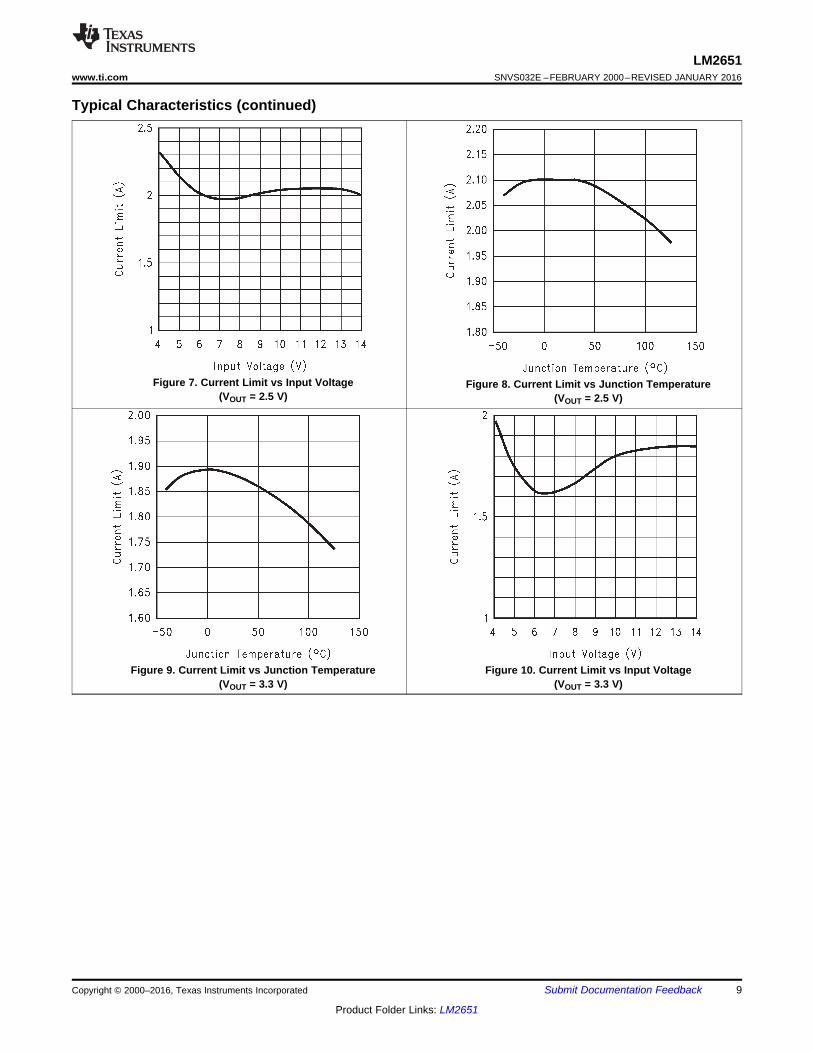
Typical Characteristics (continued)
Figure 7. Current Limit vs Input Voltage Figure 8. Current Limit vs Junction Temperature(VOUT = 2.5 V) (VOUT = 2.5 V)
Figure 9. Current Limit vs Junction Temperature Figure 10. Current Limit vs Input Voltage(VOUT = 3.3 V) (VOUT = 3.3 V)
Copyright © 2000–2016, Texas Instruments Incorporated Submit Documentation Feedback 9
Product Folder Links: LM2651

LM2651SNVS032E –FEBRUARY 2000–REVISED JANUARY 2016 www.ti.com
7 Detailed Description
7.1 OverviewThe LM2651 operates in a constant frequency (300 kHz), current-mode PWM for moderate to heavy loads, andautomatically switches to hysteretic mode for light loads. In hysteretic mode, the switching frequency is reducedto maintain high efficiency.
7.2 Functional Block Diagram
10 Submit Documentation Feedback Copyright © 2000–2016, Texas Instruments Incorporated
Product Folder Links: LM2651
LM2651www.ti.com SNVS032E –FEBRUARY 2000–REVISED JANUARY 2016
7.3 Feature DescriptionWhen the load current is higher than the sleep mode threshold, the part is always operating in PWM mode. Atthe beginning of each switching cycle, the high-side switch is turned on, the current from the high-side switch issensed and compared with the output of the error amplifier (COMP pin). When the sensed current reaches theCOMP pin voltage level, the high-side switch is turned off; after 40 ns (deadtime), the low-side switch is turnedon. At the end of the switching cycle, the low-side switch is turned off; and the same cycle repeats.
When the load current decreases below the sleep mode threshold, the output voltage rises slightly, this rise issensed by the hysteretic mode comparator which makes the part go into the hysteretic mode with both the highand low side switches off. The output voltage starts to drop until it hits the low threshold of the hystereticcomparator, and the part immediately goes back to the PWM operation. The output voltage keeps increasinguntil it reaches the top hysteretic threshold, then both the high- and low-side switches turn off again, and thecycle repeats.
7.4 Device Functional ModesThe cycle-by-cycle current limit circuitry turns off the high-side MOSFET whenever the current in MOSFETreaches 2 A. A shutdown pin is available to disable the LM2651 and reduce the supply current to 7 µA.
Copyright © 2000–2016, Texas Instruments Incorporated Submit Documentation Feedback 11
Product Folder Links: LM2651

OUT IN OUTRMS OUT
IN
V (V V )I I
V
-
= ´
LM2651SNVS032E –FEBRUARY 2000–REVISED JANUARY 2016 www.ti.com
8 Application and Implementation
NOTEInformation in the following applications sections is not part of the TI componentspecification, and TI does not warrant its accuracy or completeness. TI’s customers areresponsible for determining suitability of components for their purposes. Customers shouldvalidate and test their design implementation to confirm system functionality.
8.1 Application InformationLM2651 operates in a constant frequency (300 kHz), current-mode PWM for moderate to heavy loads; and itautomatically switches to hysteretic mode for light loads. The current of the top switch is sensed by a patentedinternal circuitry. This unique technique gets rid of the external sense resistor, saves cost and size, and improvesnoise immunity of the sensed current. A feed forward from the input voltage is added to reduce the variation ofthe current limit over the input voltage range.
8.2 Typical Application
Figure 11. Schematic for the Typical Board Layout
8.2.1 Design RequirementsTo properly size the components for the application, the designer needs the following parameters: input voltagerange, output voltage, output current range, and the switching frequency. These four main parameters affect thechoices of component available to achieve a proper system behavior. TI recommends a Schottky diode toprevent the intrinsic body diode of the low-side MOSFET from conducting during deadtime. See Detailed DesignProcedure for more information.
8.2.2 Detailed Design ProcedureThis section presents guidelines for selecting external components.
8.2.2.1 Input CapacitorA low ESR aluminum, tantalum, or ceramic capacitor is needed between the input pin and power ground. Thiscapacitor prevents large voltage transients from appearing at the input. The capacitor is selected based on theRMS current and voltage requirements. The RMS current is given by Equation 1.
(1)
12 Submit Documentation Feedback Copyright © 2000–2016, Texas Instruments Incorporated
Product Folder Links: LM2651

RIPPLE RIPPLE
S OUT
1V I ESR
8F C
æ ö= +ç ÷
è ø
( )IN OUT OUT
IN RIPPLE
V V VL
V I 300 kHz
-=
´ ´
LM2651www.ti.com SNVS032E –FEBRUARY 2000–REVISED JANUARY 2016
Typical Application (continued)The RMS current reaches its maximum (IOUT/2) when VIN equals 2 VOUT. For an aluminum or ceramic capacitor,the voltage rating should be at least 25% higher than the maximum input voltage. If a tantalum capacitor is used,the voltage rating required is about twice the maximum input voltage. The tantalum capacitor should be surge-current tested by the manufacturer to prevent being shorted by the inrush current. TI also recommends putting asmall ceramic capacitor (0.1 μF) between the input pin and ground pin to reduce high-frequency spikes.
8.2.2.2 InductorThe most critical parameters for the inductor are the inductance, peak current, and the DC resistance. Theinductance is related to the peak-to-peak inductor ripple current, the input and the output voltages, as given byEquation 2.
(2)
A higher value of ripple current reduces inductance, but increases the conductance loss, core loss, current stressfor the inductor and switch devices. It also requires a bigger output capacitor for the same output voltage ripplerequirement. A reasonable value is setting the ripple current to be 30% of the DC output current. Since the ripplecurrent increases with the input voltage, the maximum input voltage is always used to determine the inductance.The DC resistance of the inductor is a key parameter for the efficiency. Lower DC resistance is available with abigger winding area. A good tradeoff between the efficiency and the core size is letting the inductor copper lossequal 2% of the output power.
8.2.2.3 Output CapacitorThe selection of COUT is driven by the maximum allowable output voltage ripple. The output ripple in the constantfrequency, PWM mode is approximated by using Equation 3.
(3)
The ESR term usually plays the dominant role in determining the voltage ripple. A low ESR aluminum electrolyticor tantalum capacitor (such as Nichicon PL series, Sanyo OS-CON, Sprague 593D, 594D, AVX TPS, and CDEpolymer aluminum) is recommended. An electrolytic capacitor is not recommended for temperatures below−25°C since its ESR rises dramatically at cold temperature. A tantalum capacitor has a much better ESRspecification at cold temperature and is preferred for low temperature applications.
The output voltage ripple in constant frequency mode has to be less than the sleep mode voltage hysteresis toavoid entering the sleep mode at full load as given by Equation 4.
VRIPPLE < 20 mV x VOUT /VFB (4)
8.2.2.4 Boost CapacitorTI recommends a 0.1-μF ceramic capacitor for the boost capacitor. The typical voltage across the boostcapacitor is 6.7 V.
8.2.2.5 Soft-Start CapacitorA soft-start capacitor is used to provide the soft-start feature. When the input voltage is first applied, or when theSD(SS) pin is allowed to go high, the soft-start capacitor is charged by a current source (approximately 2 μA).When the SD(SS) pin voltage reaches 0.6 V (shutdown threshold), the internal regulator circuitry starts tooperate. The current charging the soft-start capacitor increases from 2 μA to approximately 10 μA. With theSD(SS) pin voltage between 0.6 V and 1.3 V, the level of the current limit is zero, which means the outputvoltage is still zero. When the SD(SS) pin voltage increases beyond 1.3 V, the current limit starts to increase.The switch duty cycle, which is controlled by the level of the current limit, starts with narrow pulses and graduallygets wider. At the same time, the output voltage of the converter increases towards the nominal value, whichbrings down the output voltage of the error amplifier. When the output of the error amplifier is less than thecurrent limit voltage, it takes over the control of the duty cycle. The converter enters the normal current-modePWM operation. The SD(SS) pin voltage is eventually charged up to about 2 V.
Copyright © 2000–2016, Texas Instruments Incorporated Submit Documentation Feedback 13
Product Folder Links: LM2651

LM2651SNVS032E –FEBRUARY 2000–REVISED JANUARY 2016 www.ti.com
Typical Application (continued)The soft-start time can be estimated using Equation 5.
TSS = CSS x 0.6 V/2 μA + CSS x (2 V − 0.6 V)/10 μA (5)
8.2.2.6 R1 and R2 (Programming Output Voltage)Use Equation 6 to select the appropriate resistor values.
VOUT = VREF(1 + R1/R2)
where• VREF = 1.238 V (6)
Select resistors between 10 kΩ and 100 kΩ. (1% or higher accuracy metal film resistors for R1 and R2.)
8.2.2.7 Compensation ComponentsIn the control to output transfer function, the first pole Fp1 can be estimated as 1/(2πROUTCOUT); The ESR zeroFz1 of the output capacitor is 1/(2πESRCOUT); Also, there is a high-frequency pole Fp2 in the range of 45 kHz to150 kHz as given by Equation 7.
Fp2 = Fs/(πn(1−D))
where• D = VOUT/VIN
• n = 1+0.348L/(VIN−VOUT) (L is in µHs and VIN and VOUT in volts). (7)
The total loop gain G is approximately 500/IOUT where IOUT is in amperes.
A Gm amplifier is used inside the LM2651. The output resistor Ro of the Gm amplifier is about 80 kΩ. Cc1 and RCtogether with Ro give a lag compensation to roll off the gain as given by Equation 8.
Fpc1 = 1/(2πCc1(Ro+Rc)), Fzc1 = 1/2πCc1Rc. (8)
In some applications, the ESR zero Fz1 cannot be cancelled by Fp2. Then, Cc2 is needed to introduce Fpc2 tocancel the ESR zero, Fp2 = 1/(2πCc2Ro‖Rc).
The rule of thumb is to have more than 45° phase margin at the crossover frequency (G = 1).
If COUT is higher than 68 µF, Cc1 = 2.2 nF, and Rc = 15 kΩ are good choices for most applications. If the ESRzero is too low to be cancelled by Fp2, add Cc2.
If the transient response to a step load is important, choose RC to be higher than 10 kΩ.
8.2.2.8 External Schottky DiodeTI recommends a Schottky diode D1 to prevent the intrinsic body diode of the low-side MOSFET from conductingduring the deadtime in PWM operation and hysteretic mode when both MOSFETs are off. If the body diode turnson, there is extra power dissipation in the body diode because of the reverse-recovery current and higher forwardvoltage; the high-side MOSFET also has more switching loss since the negative diode reverse-recovery currentappears as the high-side MOSFET turnon current in addition to the load current. These losses degrade theefficiency by 1–2%. The improved efficiency and noise immunity with the Schottky diode become more obviouswith increasing input voltage and load current.
The breakdown voltage rating of D1 is preferred to be 25% higher than the maximum input voltage. Since D1 isonly on for a short period of time, the average current rating for D1 only requires being higher than 30% of themaximum output current. It is important to place D1 very close to the drain and source of the low-side MOSFET,extra parasitic inductance in the parallel loop slows the turnon of D1 and direct the current through the bodydiode of the low-side MOSFET.
When an undervoltage situation occurs, the output voltage can be pulled below ground as the inductor current isreversed through the synchronous FET. For applications that require protection from a negative voltage, TIrecommends a clamping diode D2. When used, D2 should be connected cathode to VOUT and anode to ground.TI recommends a diode rated for a minimum of 2 A.
14 Submit Documentation Feedback Copyright © 2000–2016, Texas Instruments Incorporated
Product Folder Links: LM2651

LM2651www.ti.com SNVS032E –FEBRUARY 2000–REVISED JANUARY 2016
Typical Application (continued)8.2.3 Application Curves
(VIN = 5 V, VOUT = 3.3 V)
Figure 13. Sleep Mode Threshold vs Output VoltageFigure 12. Efficiency vs Load CurrentFor ADJ Version (VIN = 5 V)
Copyright © 2000–2016, Texas Instruments Incorporated Submit Documentation Feedback 15
Product Folder Links: LM2651

LM2651SNVS032E –FEBRUARY 2000–REVISED JANUARY 2016 www.ti.com
9 Power Supply RecommendationsThe LM2651 is designed to operate from various DC power supplies. If so, VIN input should be protected fromreversal voltage and voltage dump over 15 V. The impedance of the input supply rail should be low enough thatthe input current transient does not cause drop below VIN UVLO level. If the input supply is connected by usinglong wires, additional bulk capacitance may be required in addition to normal input capacitor.
10 Layout
10.1 Layout GuidelinesLayout is critical to reduce noises and ensure specified performance. The important guidelines are listed asfollows:1. Minimize the parasitic inductance in the loop of input capacitors and the internal MOSFETs by connecting the
input capacitors to VIN and PGND pins with short and wide traces. This is important because the rapidlyswitching current, together with wiring inductance can generate large voltage spikes that may result in noiseproblems.
2. Minimize the trace from the center of the output resistor divider to the FB pin and keep it away from noisesources to avoid noise pickup. For applications requiring tight regulation at the output, TI recommends adedicated sense trace (separated from the power trace) to connect the top of the resistor divider to theoutput.
3. If the Schottky diode D1 is used, minimize the traces connecting D1 to SW and PGND pins.
10.2 Layout Example
Figure 14. LM2651 Layout Recommendation
16 Submit Documentation Feedback Copyright © 2000–2016, Texas Instruments Incorporated
Product Folder Links: LM2651

LM2651www.ti.com SNVS032E –FEBRUARY 2000–REVISED JANUARY 2016
11 Device and Documentation Support
11.1 Community ResourcesThe following links connect to TI community resources. Linked contents are provided "AS IS" by the respectivecontributors. They do not constitute TI specifications and do not necessarily reflect TI's views; see TI's Terms ofUse.
TI E2E™ Online Community TI's Engineer-to-Engineer (E2E) Community. Created to foster collaborationamong engineers. At e2e.ti.com, you can ask questions, share knowledge, explore ideas and helpsolve problems with fellow engineers.
Design Support TI's Design Support Quickly find helpful E2E forums along with design support tools andcontact information for technical support.
11.2 TrademarksE2E is a trademark of Texas Instruments.All other trademarks are the property of their respective owners.
11.3 Electrostatic Discharge CautionThese devices have limited built-in ESD protection. The leads should be shorted together or the device placed in conductive foamduring storage or handling to prevent electrostatic damage to the MOS gates.
11.4 GlossarySLYZ022 — TI Glossary.
This glossary lists and explains terms, acronyms, and definitions.
12 Mechanical, Packaging, and Orderable InformationThe following pages include mechanical, packaging, and orderable information. This information is the mostcurrent data available for the designated devices. This data is subject to change without notice and revision ofthis document. For browser-based versions of this data sheet, refer to the left-hand navigation.
Copyright © 2000–2016, Texas Instruments Incorporated Submit Documentation Feedback 17
Product Folder Links: LM2651

PACKAGE OPTION ADDENDUM
www.ti.com 27-Oct-2016
Addendum-Page 1
PACKAGING INFORMATION
Orderable Device Status(1)
Package Type PackageDrawing
Pins PackageQty
Eco Plan(2)
Lead/Ball Finish(6)
MSL Peak Temp(3)
Op Temp (°C) Device Marking(4/5)
Samples
LM2651MTC-3.3/NOPB ACTIVE TSSOP PW 16 92 Green (RoHS& no Sb/Br)
CU SN Level-1-260C-UNLIM -40 to 125 2651MTC-3.3
LM2651MTC-ADJ NRND TSSOP PW 16 92 TBD Call TI Call TI -40 to 125 2651MTC-ADJ
LM2651MTC-ADJ/NOPB ACTIVE TSSOP PW 16 92 Green (RoHS& no Sb/Br)
CU SN Level-1-260C-UNLIM -40 to 125 2651MTC-ADJ
LM2651MTCX-3.3/NOPB ACTIVE TSSOP PW 16 2500 Green (RoHS& no Sb/Br)
CU SN Level-1-260C-UNLIM -40 to 125 2651MTC-3.3
LM2651MTCX-ADJ/NOPB ACTIVE TSSOP PW 16 2500 Green (RoHS& no Sb/Br)
CU SN Level-1-260C-UNLIM -40 to 125 2651MTC-ADJ
(1) The marketing status values are defined as follows:ACTIVE: Product device recommended for new designs.LIFEBUY: TI has announced that the device will be discontinued, and a lifetime-buy period is in effect.NRND: Not recommended for new designs. Device is in production to support existing customers, but TI does not recommend using this part in a new design.PREVIEW: Device has been announced but is not in production. Samples may or may not be available.OBSOLETE: TI has discontinued the production of the device.
(2) Eco Plan - The planned eco-friendly classification: Pb-Free (RoHS), Pb-Free (RoHS Exempt), or Green (RoHS & no Sb/Br) - please check http://www.ti.com/productcontent for the latest availabilityinformation and additional product content details.TBD: The Pb-Free/Green conversion plan has not been defined.Pb-Free (RoHS): TI's terms "Lead-Free" or "Pb-Free" mean semiconductor products that are compatible with the current RoHS requirements for all 6 substances, including the requirement thatlead not exceed 0.1% by weight in homogeneous materials. Where designed to be soldered at high temperatures, TI Pb-Free products are suitable for use in specified lead-free processes.Pb-Free (RoHS Exempt): This component has a RoHS exemption for either 1) lead-based flip-chip solder bumps used between the die and package, or 2) lead-based die adhesive used betweenthe die and leadframe. The component is otherwise considered Pb-Free (RoHS compatible) as defined above.Green (RoHS & no Sb/Br): TI defines "Green" to mean Pb-Free (RoHS compatible), and free of Bromine (Br) and Antimony (Sb) based flame retardants (Br or Sb do not exceed 0.1% by weightin homogeneous material)
(3) MSL, Peak Temp. - The Moisture Sensitivity Level rating according to the JEDEC industry standard classifications, and peak solder temperature.
(4) There may be additional marking, which relates to the logo, the lot trace code information, or the environmental category on the device.
(5) Multiple Device Markings will be inside parentheses. Only one Device Marking contained in parentheses and separated by a "~" will appear on a device. If a line is indented then it is a continuationof the previous line and the two combined represent the entire Device Marking for that device.

PACKAGE OPTION ADDENDUM
www.ti.com 27-Oct-2016
Addendum-Page 2
(6) Lead/Ball Finish - Orderable Devices may have multiple material finish options. Finish options are separated by a vertical ruled line. Lead/Ball Finish values may wrap to two lines if the finishvalue exceeds the maximum column width.
Important Information and Disclaimer:The information provided on this page represents TI's knowledge and belief as of the date that it is provided. TI bases its knowledge and belief on informationprovided by third parties, and makes no representation or warranty as to the accuracy of such information. Efforts are underway to better integrate information from third parties. TI has taken andcontinues to take reasonable steps to provide representative and accurate information but may not have conducted destructive testing or chemical analysis on incoming materials and chemicals.TI and TI suppliers consider certain information to be proprietary, and thus CAS numbers and other limited information may not be available for release.
In no event shall TI's liability arising out of such information exceed the total purchase price of the TI part(s) at issue in this document sold by TI to Customer on an annual basis.

TAPE AND REEL INFORMATION
*All dimensions are nominal
Device PackageType
PackageDrawing
Pins SPQ ReelDiameter
(mm)
ReelWidth
W1 (mm)
A0(mm)
B0(mm)
K0(mm)
P1(mm)
W(mm)
Pin1Quadrant
LM2651MTCX-3.3/NOPB TSSOP PW 16 2500 330.0 12.4 6.95 5.6 1.6 8.0 12.0 Q1
LM2651MTCX-ADJ/NOPB TSSOP PW 16 2500 330.0 12.4 6.95 5.6 1.6 8.0 12.0 Q1
PACKAGE MATERIALS INFORMATION
www.ti.com 6-Nov-2015
Pack Materials-Page 1

*All dimensions are nominal
Device Package Type Package Drawing Pins SPQ Length (mm) Width (mm) Height (mm)
LM2651MTCX-3.3/NOPB TSSOP PW 16 2500 367.0 367.0 35.0
LM2651MTCX-ADJ/NOPB TSSOP PW 16 2500 367.0 367.0 35.0
PACKAGE MATERIALS INFORMATION
www.ti.com 6-Nov-2015
Pack Materials-Page 2


IMPORTANT NOTICE
Texas Instruments Incorporated and its subsidiaries (TI) reserve the right to make corrections, enhancements, improvements and otherchanges to its semiconductor products and services per JESD46, latest issue, and to discontinue any product or service per JESD48, latestissue. Buyers should obtain the latest relevant information before placing orders and should verify that such information is current andcomplete. All semiconductor products (also referred to herein as “components”) are sold subject to TI’s terms and conditions of salesupplied at the time of order acknowledgment.TI warrants performance of its components to the specifications applicable at the time of sale, in accordance with the warranty in TI’s termsand conditions of sale of semiconductor products. Testing and other quality control techniques are used to the extent TI deems necessaryto support this warranty. Except where mandated by applicable law, testing of all parameters of each component is not necessarilyperformed.TI assumes no liability for applications assistance or the design of Buyers’ products. Buyers are responsible for their products andapplications using TI components. To minimize the risks associated with Buyers’ products and applications, Buyers should provideadequate design and operating safeguards.TI does not warrant or represent that any license, either express or implied, is granted under any patent right, copyright, mask work right, orother intellectual property right relating to any combination, machine, or process in which TI components or services are used. Informationpublished by TI regarding third-party products or services does not constitute a license to use such products or services or a warranty orendorsement thereof. Use of such information may require a license from a third party under the patents or other intellectual property of thethird party, or a license from TI under the patents or other intellectual property of TI.Reproduction of significant portions of TI information in TI data books or data sheets is permissible only if reproduction is without alterationand is accompanied by all associated warranties, conditions, limitations, and notices. TI is not responsible or liable for such altereddocumentation. Information of third parties may be subject to additional restrictions.Resale of TI components or services with statements different from or beyond the parameters stated by TI for that component or servicevoids all express and any implied warranties for the associated TI component or service and is an unfair and deceptive business practice.TI is not responsible or liable for any such statements.Buyer acknowledges and agrees that it is solely responsible for compliance with all legal, regulatory and safety-related requirementsconcerning its products, and any use of TI components in its applications, notwithstanding any applications-related information or supportthat may be provided by TI. Buyer represents and agrees that it has all the necessary expertise to create and implement safeguards whichanticipate dangerous consequences of failures, monitor failures and their consequences, lessen the likelihood of failures that might causeharm and take appropriate remedial actions. Buyer will fully indemnify TI and its representatives against any damages arising out of the useof any TI components in safety-critical applications.In some cases, TI components may be promoted specifically to facilitate safety-related applications. With such components, TI’s goal is tohelp enable customers to design and create their own end-product solutions that meet applicable functional safety standards andrequirements. Nonetheless, such components are subject to these terms.No TI components are authorized for use in FDA Class III (or similar life-critical medical equipment) unless authorized officers of the partieshave executed a special agreement specifically governing such use.Only those TI components which TI has specifically designated as military grade or “enhanced plastic” are designed and intended for use inmilitary/aerospace applications or environments. Buyer acknowledges and agrees that any military or aerospace use of TI componentswhich have not been so designated is solely at the Buyer's risk, and that Buyer is solely responsible for compliance with all legal andregulatory requirements in connection with such use.TI has specifically designated certain components as meeting ISO/TS16949 requirements, mainly for automotive use. In any case of use ofnon-designated products, TI will not be responsible for any failure to meet ISO/TS16949.
Products ApplicationsAudio www.ti.com/audio Automotive and Transportation www.ti.com/automotiveAmplifiers amplifier.ti.com Communications and Telecom www.ti.com/communicationsData Converters dataconverter.ti.com Computers and Peripherals www.ti.com/computersDLP® Products www.dlp.com Consumer Electronics www.ti.com/consumer-appsDSP dsp.ti.com Energy and Lighting www.ti.com/energyClocks and Timers www.ti.com/clocks Industrial www.ti.com/industrialInterface interface.ti.com Medical www.ti.com/medicalLogic logic.ti.com Security www.ti.com/securityPower Mgmt power.ti.com Space, Avionics and Defense www.ti.com/space-avionics-defenseMicrocontrollers microcontroller.ti.com Video and Imaging www.ti.com/videoRFID www.ti-rfid.comOMAP Applications Processors www.ti.com/omap TI E2E Community e2e.ti.comWireless Connectivity www.ti.com/wirelessconnectivity
Mailing Address: Texas Instruments, Post Office Box 655303, Dallas, Texas 75265Copyright © 2016, Texas Instruments Incorporated