lm2585 simple switcher 3a flyback regulatordocs-europe.electrocomponents.com/webdocs/0780/... ·...
TRANSCRIPT
LM2585SIMPLE SWITCHER® 3A Flyback RegulatorGeneral DescriptionThe LM2585 series of regulators are monolithic integratedcircuits specifically designed for flyback, step-up (boost), andforward converter applications. The device is available in 4different output voltage versions: 3.3V, 5.0V, 12V, and ad-justable.
Requiring a minimum number of external components, theseregulators are cost effective, and simple to use. Included inthe datasheet are typical circuits of boost and flyback regu-lators. Also listed are selector guides for diodes and capaci-tors and a family of standard inductors and flyback trans-formers designed to work with these switching regulators.
The power switch is a 3.0A NPN device that can stand-off65V. Protecting the power switch are current and thermallimiting circuits, and an undervoltage lockout circuit. This ICcontains a 100 kHz fixed-frequency internal oscillator thatpermits the use of small magnetics. Other features includesoft start mode to reduce in-rush current during start up,current mode control for improved rejection of input voltageand output load transients and cycle-by-cycle current limit-ing. An output voltage tolerance of ±4%, within specifiedinput voltages and output load conditions, is guaranteed forthe power supply system.
Featuresn Requires few external componentsn Family of standard inductors and transformersn NPN output switches 3.0A, can stand off 65Vn Wide input voltage range: 4V to 40Vn Current-mode operation for improved transient
response, line regulation, and current limitn 100 kHz switching frequencyn Internal soft-start function reduces in-rush current during
start-upn Output transistor protected by current limit, under
voltage lockout, and thermal shutdownn System Output Voltage Tolerance of ±4% max over line
and load conditions
Typical Applicationsn Flyback regulatorn Multiple-output regulatorn Simple boost regulatorn Forward converter
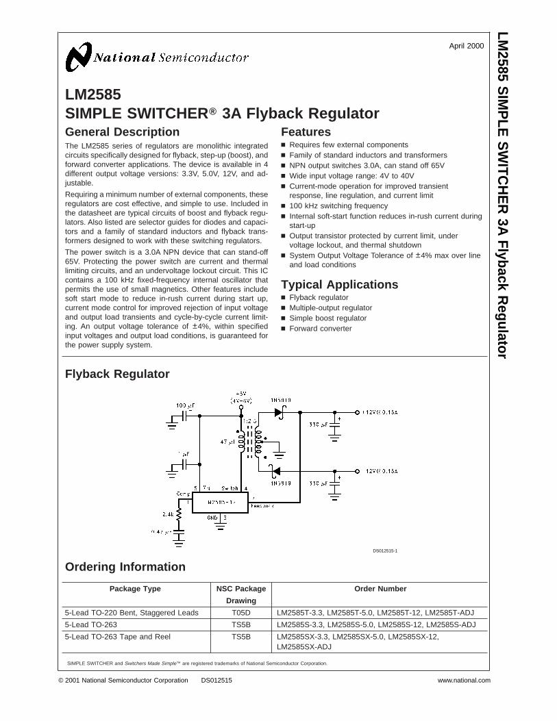
Flyback Regulator
Ordering Information
Package Type NSC Package Order Number
Drawing
5-Lead TO-220 Bent, Staggered Leads T05D LM2585T-3.3, LM2585T-5.0, LM2585T-12, LM2585T-ADJ
5-Lead TO-263 TS5B LM2585S-3.3, LM2585S-5.0, LM2585S-12, LM2585S-ADJ
5-Lead TO-263 Tape and Reel TS5B LM2585SX-3.3, LM2585SX-5.0, LM2585SX-12,LM2585SX-ADJ
SIMPLE SWITCHER and Switchers Made Simple™ are registered trademarks of National Semiconductor Corporation.
DS012515-1
April 2000LM
2585S
IMP
LES
WITC
HE
R3A
FlybackR
egulator
© 2001 National Semiconductor Corporation DS012515 www.national.com
Absolute Maximum Ratings (Note 1)
If Military/Aerospace specified devices are required,please contact the National Semiconductor Sales Office/Distributors for availability and specifications.
Input Voltage −0.4V ≤ VIN ≤ 45VSwitch Voltage −0.4V ≤ VSW ≤ 65VSwitch Current (Note 2) Internally LimitedCompensation Pin Voltage −0.4V ≤ VCOMP ≤ 2.4VFeedback Pin Voltage −0.4V ≤ VFB ≤ 2 VOUT
Storage Temperature Range −65˚C to +150˚CLead Temperature
(Soldering, 10 sec.) 260˚C
Maximum Junction Temperature(Note 3) 150˚C
Power Dissipation (Note 3) Internally LimitedMinimum ESD Rating
(C = 100 pF, R = 1.5 kΩ) 2 kV
Operating RatingsSupply Voltage 4V ≤ VIN ≤ 40VOutput Switch Voltage 0V ≤ VSW ≤ 60VOutput Switch Current ISW ≤ 3.0AJunction Temperature Range −40˚C ≤ TJ ≤ +125˚C
Electrical CharacteristicsLM2585-3.3Specifications with standard type face are for TJ = 25˚C, and those in bold type face apply over full Operating TemperatureRange. Unless otherwise specified, VIN = 5V.
Symbol Parameters Conditions Typical Min Max Units
SYSTEM PARAMETERS Test Circuit of Figure 2 (Note 4)
VOUT Output Voltage VIN = 4V to 12V 3.3 3.17/3.14 3.43/3.46 V
ILOAD = 0.3A to 1.2A
∆VOUT/ Line Regulation VIN = 4V to 12V 20 50/100 mV
∆VIN ILOAD = 0.3A
∆VOUT/ Load Regulation VIN = 12V 20 50/100 mV
∆ILOAD ILOAD = 0.3A to 1.2A
η Efficiency VIN = 5V, ILOAD = 0.3A 76 %
UNIQUE DEVICE PARAMETERS (Note 5)
VREF Output Reference Measured at Feedback Pin 3.3 3.242/3.234 3.358/3.366 V
Voltage VCOMP = 1.0V
∆VREF Reference Voltage VIN = 4V to 40V 2.0 mV
Line Regulation
GM Error Amp ICOMP = −30 µA to +30 µA 1.193 0.678 2.259 mmho
Transconductance VCOMP = 1.0V
AVOL Error Amp VCOMP = 0.5V to 1.6V 260 151/75 V/V
Voltage Gain RCOMP = 1.0 MΩ (Note 6)
LM2585-5.0Symbol Parameters Conditions Typical Min Max Units
SYSTEM PARAMETERS Test Circuit of Figure 2 (Note 4)
VOUT Output Voltage VIN = 4V to 12V 5.0 4.80/4.75 5.20/5.25 V
ILOAD = 0.3A to 1.1A
∆VOUT/ Line Regulation VIN = 4V to 12V 20 50/100 mV
∆VIN ILOAD = 0.3A
∆VOUT/ Load Regulation VIN = 12V 20 50/100 mV
∆ILOAD ILOAD = 0.3A to 1.1A
η Efficiency VIN = 12V, ILOAD = 0.6A 80 %
UNIQUE DEVICE PARAMETERS (Note 5)
VREF Output Reference Measured at Feedback Pin 5.0 4.913/4.900 5.088/5.100 V
Voltage VCOMP = 1.0V
∆VREF Reference Voltage VIN = 4V to 40V 3.3 mV
Line Regulation
LM25
85
www.national.com 2

LM2585-5.0 (Continued)
Symbol Parameters Conditions Typical Min Max Units
UNIQUE DEVICE PARAMETERS (Note 5)
GM Error Amp ICOMP = −30 µA to +30 µA 0.750 0.447 1.491 mmho
Transconductance VCOMP = 1.0V
AVOL Error Amp VCOMP = 0.5V to 1.6V 165 99/49 V/V
Voltage Gain RCOMP = 1.0 MΩ (Note 6)
LM2585-12Symbol Parameters Conditions Typical Min Max Units
SYSTEM PARAMETERS Test Circuit of Figure 3 (Note 4)
VOUT Output Voltage VIN = 4V to 10V 12.0 11.52/11.40 12.48/12.60 V
ILOAD = 0.2A to 0.8A
∆VOUT/ Line Regulation VIN = 4V to 10V 20 100/200 mV
∆VIN ILOAD = 0.2A
∆VOUT/ Load Regulation VIN = 10V 20 100/200 mV
∆ILOAD ILOAD = 0.2A to 0.8A
η Efficiency VIN = 10V, ILOAD = 0.6A 93 %
UNIQUE DEVICE PARAMETERS (Note 5)
VREF Output Reference Measured at Feedback Pin 12.0 11.79/11.76 12.21/12.24 V
Voltage VCOMP = 1.0V
∆VREF Reference Voltage VIN = 4V to 40V 7.8 mV
Line Regulation
GM Error Amp ICOMP = −30 µA to +30 µA 0.328 0.186 0.621 mmho
Transconductance VCOMP = 1.0V
AVOL Error Amp VCOMP = 0.5V to 1.6V 70 41/21 V/V
Voltage Gain RCOMP = 1.0 MΩ (Note 6)
LM2585-ADJSymbol Parameters Conditions Typical Min Max Units
SYSTEM PARAMETERS Test Circuit of Figure 3 (Note 4)
VOUT Output Voltage VIN = 4V to 10V 12.0 11.52/11.40 12.48/12.60 V
ILOAD = 0.2A to 0.8A
∆VOUT/ Line Regulation VIN = 4V to 10V 20 100/200 mV
∆VIN ILOAD = 0.2A
∆VOUT/ Load Regulation VIN = 10V 20 100/200 mV
∆ILOAD ILOAD = 0.2A to 0.8A
η Efficiency VIN = 10V, ILOAD = 0.6A 93 %
UNIQUE DEVICE PARAMETERS (Note 5)
VREF Output Reference Measured at Feedback Pin 1.230 1.208/1.205 1.252/1.255 V
Voltage VCOMP = 1.0V
∆VREF Reference Voltage VIN = 4V to 40V 1.5 mV
Line Regulation
GM Error Amp ICOMP = −30 µA to +30 µA 3.200 1.800 6.000 mmho
Transconductance VCOMP = 1.0V
AVOL Error Amp VCOMP = 0.5V to 1.6V 670 400/200 V/V
Voltage Gain RCOMP = 1.0 MΩ (Note 6)
IB Error Amp VCOMP = 1.0V 125 425/600 nA
Input Bias Current
LM2585
www.national.com3

Electrical Characteristics (All Versions)Symbol Parameters Conditions Typical Min Max Units
COMMON DEVICE PARAMETERS for all versions (Note 5)
IS Input Supply (Switch Off) 11 15.5/16.5 mA
Current (Note 8)
ISWITCH = 1.8A 50 100/115 mA
VUV Input Supply RLOAD = 100Ω 3.30 3.05 3.75 V
UndervoltageLockout
fO Oscillator Frequency Measured at Switch Pin
RLOAD = 100Ω 100 85/75 115/125 kHz
VCOMP = 1.0V
fSC Short-Circuit Measured at Switch Pin
Frequency RLOAD = 100Ω 25 kHz
VFEEDBACK = 1.15V
VEAO Error Amplifier Upper Limit 2.8 2.6/2.4 V
Output Swing (Note 7)
Lower Limit 0.25 0.40/0.55 V
(Note 8)
IEAO Error Amp (Note 9)
Output Current 165 110/70 260/320 µA
(Source or Sink)
ISS Soft Start Current VFEEDBACK = 0.92V 11.0 8.0/7.0 17.0/19.0 µA
VCOMP = 1.0V
D Maximum Duty RLOAD = 100Ω 98 93/90 %
Cycle (Note 7)
IL Switch Leakage Switch Off 15 300/600 µA
Current VSWITCH = 60V
VSUS Switch Sustaining dV/dT = 1.5V/ns 65 V
Voltage
VSAT Switch Saturation ISWITCH = 3.0A 0.45 0.65/0.9 V
Voltage
ICL NPN Switch 4.0 3.0 7.0 A
Current Limit
θJA Thermal Resistance T Package, Junction toAmbient (Note 10)
65
θJA T Package, Junction toAmbient (Note 11)
45
θJC T Package, Junction toCase
2
θJA S Package, Junction toAmbient (Note 12)
56˚C/W
θJA S Package, Junction toAmbient (Note 13)
35
θJA S Package, Junction toAmbient (Note 14)
26
θJC S Package, Junction toCase
2
Note 1: Absolute Maximum Ratings indicate limits beyond which damage to the device may occur. Operating ratings indicate conditions the device is intended tobe functional, but device parameter specifications may not be guaranteed under these conditions. For guaranteed specifications and test conditions, see theElectrical Characteristics.
Note 2: Note that switch current and output current are not identical in a step-up regulator. Output current cannot be internally limited when the LM2585 is used asa step-up regulator. To prevent damage to the switch, the output current must be externally limited to 3A. However, output current is internally limited when theLM2585 is used as a flyback regulator (see the Application Hints section for more information).
LM25
85
www.national.com 4

Electrical Characteristics (All Versions) (Continued)
Note 3: The junction temperature of the device (TJ) is a function of the ambient temperature (TA), the junction-to-ambient thermal resistance (θJA), and the powerdissipation of the device (PD). A thermal shutdown will occur if the temperature exceeds the maximum junction temperature of the device: PD x θJA + TA(MAX) ≥TJ(MAX). For a safe thermal design, check that the maximum power dissipated by the device is less than: PD ≤ [TJ(MAX) − TA(MAX))]/θJA. When calculating themaximum allowable power dissipation, derate the maximum junction temperature — this ensures a margin of safety in the thermal design.
Note 4: External components such as the diode, inductor, input and output capacitors can affect switching regulator performance. When the LM2585 is used asshown in Figures Figure 2 and Figure 3 , system performance will be as specified by the system parameters.
Note 5: All room temperature limits are 100% production tested, and all limits at temperature extremes are guaranteed via correlation using standard StatisticalQuality Control (SQC) methods.
Note 6: A 1.0 MΩ resistor is connected to the compensation pin (which is the error amplifier output) to ensure accuracy in measuring AVOL.
Note 7: To measure this parameter, the feedback voltage is set to a low value, depending on the output version of the device, to force the error amplifier output high.Adj: VFB = 1.05V; 3.3V: VFB = 2.81V; 5.0V: VFB = 4.25V; 12V: VFB = 10.20V.
Note 8: To measure this parameter, the feedback voltage is set to a high value, depending on the output version of the device, to force the error amplifier outputlow. Adj: VFB = 1.41V; 3.3V: VFB = 3.80V; 5.0V: VFB = 5.75V; 12V: VFB = 13.80V.
Note 9: To measure the worst-case error amplifier output current, the LM2585 is tested with the feedback voltage set to its low value (specified in (Note 7) and atits high value (specified in (Note 8) .
Note 10: Junction to ambient thermal resistance (no external heat sink) for the 5 lead TO-220 package mounted vertically, with 1⁄2 inch leads in a socket, or on aPC board with minimum copper area.
Note 11: Junction to ambient thermal resistance (no external heat sink) for the 5 lead TO-220 package mounted vertically, with 1⁄2 inch leads soldered to a PC boardcontaining approximately 4 square inches of (1oz.) copper area surrounding the leads.
Note 12: Junction to ambient thermal resistance for the 5 lead TO-263 mounted horizontally against a PC board area of 0.136 square inches (the same size as theTO-263 package) of 1 oz. (0.0014 in. thick) copper.
Note 13: Junction to ambient thermal resistance for the 5 lead TO-263 mounted horizontally against a PC board area of 0.4896 square inches (3.6 times the areaof the TO-263 package) of 1 oz. (0.0014 in. thick) copper.
Note 14: Junction to ambient thermal resistance for the 5 lead TO-263 mounted horizontally against a PC board copper area of 1.0064 square inches (7.4 timesthe area of the TO-263 package) of 1 oz. (0.0014 in. thick) copper. Additional copper area will reduce thermal resistance further. See the thermal model in SwitchersMade Simple software.
Typical Performance Characteristics
Supply Currentvs Temperature
DS012515-2
Reference Voltagevs Temperature
DS012515-3
∆Reference Voltagevs Supply Voltage
DS012515-4
Supply Currentvs Switch Current
DS012515-5
Current Limitvs Temperature
DS012515-6
Feedback Pin BiasCurrent vs Temperature
DS012515-7
LM2585
www.national.com5
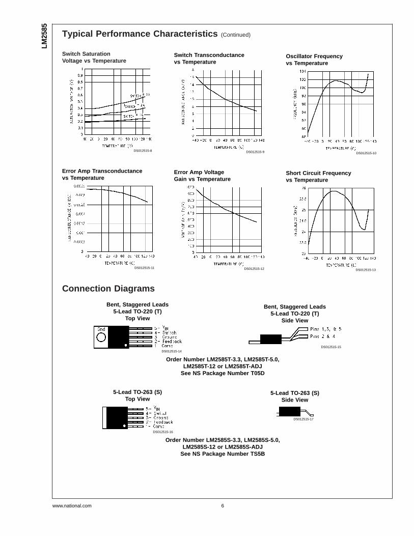
Typical Performance Characteristics (Continued)
Connection Diagrams
Switch SaturationVoltage vs Temperature
DS012515-8
Switch Transconductancevs Temperature
DS012515-9
Oscillator Frequencyvs Temperature
DS012515-10
Error Amp Transconductancevs Temperature
DS012515-11
Error Amp VoltageGain vs Temperature
DS012515-12
Short Circuit Frequencyvs Temperature
DS012515-13
Bent, Staggered Leads5-Lead TO-220 (T)
Top View
DS012515-14
Bent, Staggered Leads5-Lead TO-220 (T)
Side View
DS012515-15
Order Number LM2585T-3.3, LM2585T-5.0,LM2585T-12 or LM2585T-ADJ
See NS Package Number T05D
5-Lead TO-263 (S)Top View
DS012515-16
5-Lead TO-263 (S)Side View
DS012515-17
Order Number LM2585S-3.3, LM2585S-5.0,LM2585S-12 or LM2585S-ADJ
See NS Package Number TS5B
LM25
85
www.national.com 6
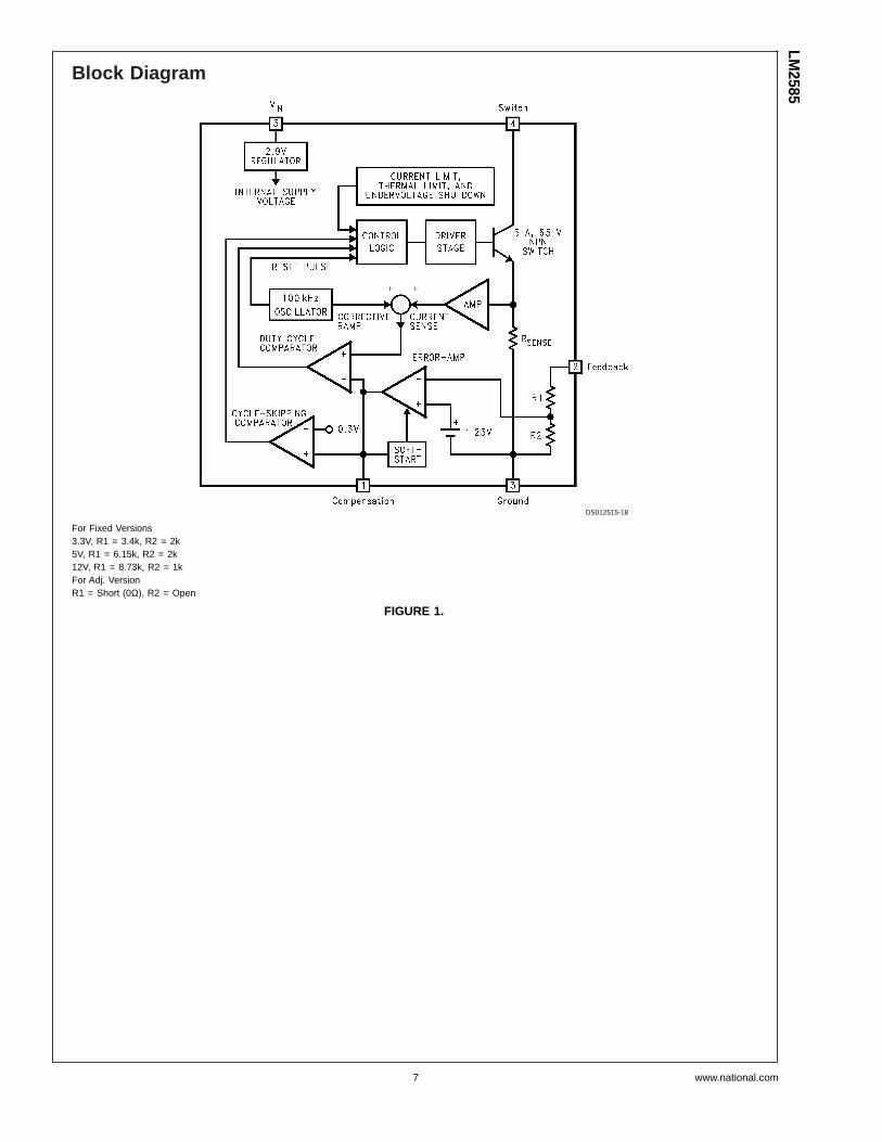
Block Diagram
DS012515-18
For Fixed Versions3.3V, R1 = 3.4k, R2 = 2k5V, R1 = 6.15k, R2 = 2k12V, R1 = 8.73k, R2 = 1kFor Adj. VersionR1 = Short (0Ω), R2 = Open
FIGURE 1.
LM2585
www.national.com7

Test Circuits
DS012515-19
CIN1 — 100 µF, 25V Aluminum ElectrolyticCIN2 — 0.1 µF CeramicT — 22 µH, 1:1 Schott #67141450D — 1N5820COUT — 680 µF, 16V Aluminum ElectrolyticCC — 0.47 µF CeramicRC — 2k
FIGURE 2. LM2585-3.3 and LM2585-5.0
DS012515-20
CIN1 — 100 µF, 25V Aluminum ElectrolyticCIN2 — 0.1 µF CeramicL — 15 µH, Renco #RL-5472-5D — 1N5820COUT — 680 µF, 16V Aluminum ElectrolyticCC — 0.47 µF CeramicRC — 2kFor 12V Devices: R1 = Short (0Ω) and R2 = OpenFor ADJ Devices: R1 = 48.75k, ±0.1% and R2 = 5.62k, ±1%
FIGURE 3. LM2585-12 and LM2585-ADJ
LM25
85
www.national.com 8

Flyback Regulator OperationThe LM2585 is ideally suited for use in the flyback regulatortopology. The flyback regulator can produce a single outputvoltage, such as the one shown in Figure 4, or multipleoutput voltages. In Figure 4, the flyback regulator generatesan output voltage that is inside the range of the input voltage.This feature is unique to flyback regulators and cannot beduplicated with buck or boost regulators.
The operation of a flyback regulator is as follows (refer toFigure 4): when the switch is on, current flows through theprimary winding of the transformer, T1, storing energy in themagnetic field of the transformer. Note that the primary andsecondary windings are out of phase, so no current flowsthrough the secondary when current flows through the pri-mary. When the switch turns off, the magnetic field col-
lapses, reversing the voltage polarity of the primary andsecondary windings. Now rectifier D1 is forward biased andcurrent flows through it, releasing the energy stored in thetransformer. This produces voltage at the output.
The output voltage is controlled by modulating the peakswitch current. This is done by feeding back a portion of theoutput voltage to the error amp, which amplifies the differ-ence between the feedback voltage and a 1.230V reference.The error amp output voltage is compared to a ramp voltageproportional to the switch current (i.e., inductor current dur-ing the switch on time). The comparator terminates theswitch on time when the two voltages are equal, therebycontrolling the peak switch current to maintain a constantoutput voltage.
DS012515-21
As shown in Figure 4, the LM2585 can be used as a flyback regulator by using a minimum number of external components. The switching waveforms of thisregulator are shown in Figure 5. Typical Performance Characteristics observed during the operation of this circuit are shown in Figure 6.
FIGURE 4. 12V Flyback Regulator Design Example
DS012515-22
A: Switch Voltage, 20 V/divB: Switch Current, 2 A/divC: Output Rectifier Current, 2 A/divD: Output Ripple Voltage, 50 mV/divAC-CoupledHorizontal: 2 µs/div
FIGURE 5. Switching Waveforms
LM2585
www.national.com9

Flyback Regulator Operation (Continued)
Typical Flyback Regulator ApplicationsFigure 7 through Figure 12 show six typical flyback applica-tions, varying from single output to triple output. Each draw-ing contains the part number(s) and manufacturer(s) forevery component except the transformer. For the trans-former part numbers and manufacturers names, see the
table in Figure 13. For applications with different outputvoltages — requiring the LM2585-ADJ — or different outputconfigurations that do not match the standard configurations,refer to the Switchers Made Simple ® software.
DS012515-23
FIGURE 6. VOUT Load Current Step Response
DS012515-24
FIGURE 7. Single-Output Flyback Regulator
LM25
85
www.national.com 10

Typical Flyback Regulator Applications (Continued)
DS012515-25
FIGURE 8. Single-Output Flyback Regulator
DS012515-26
FIGURE 9. Single-Output Flyback Regulator
LM2585
www.national.com11
Typical Flyback Regulator Applications (Continued)
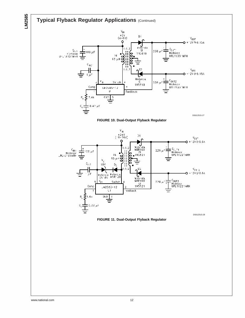
DS012515-27
FIGURE 10. Dual-Output Flyback Regulator
DS012515-28
FIGURE 11. Dual-Output Flyback Regulator
LM25
85
www.national.com 12
Typical Flyback Regulator Applications (Continued)
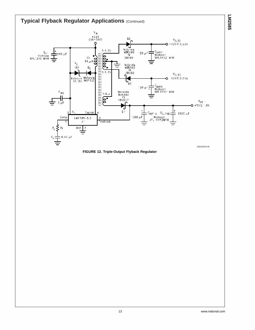
DS012515-29
FIGURE 12. Triple-Output Flyback Regulator
LM2585
www.national.com13

Typical Flyback Regulator Applications (Continued)
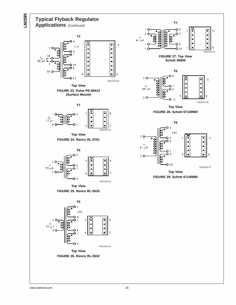
Transformer Selection (T)
Figure 13 lists the standard transformers available for flyback regulator applications. Included in the table are the turns ratio(s) foreach transformer, as well as the output voltages, input voltage ranges, and the maximum load currents for each circuit.
Applications Figure 7 Figure 8 Figure 9 Figure 10 Figure 11 Figure 12
Transformers T7 T7 T7 T6 T6 T5
VIN 4V–6V 4V–6V 8V–16V 4V–6V 18V–36V 18V–36V
VOUT1 3.3V 5V 12V 12V 12V 5V
IOUT1 (Max) 1.4A 1A 0.8A 0.15A 0.6A 1.8A
N1 1 1 1 1.2 1.2 0.5
VOUT2 −12V −12V 12V
IOUT2 (Max) 0.15A 0.6A 0.25A
N2 1.2 1.2 1.15
VOUT3 −12V
IOUT3 (Max) 0.25A
N3 1.15
FIGURE 13. Transformer Selection Table
Trans-formerType
Manufacturers’ Part Numbers
Coilcraft Coilcraft Pulse Pulse Renco Schott
(Note 15) (Note 15) (Note 16) (Note 16) (Note 17) (Note 18)
Surface Mount Surface Mount
T5 Q4338-B Q4437-B PE-68413 — RL-5532 67140890
T6 Q4339-B Q4438-B PE-68414 — RL-5533 67140900
T7 S6000-A S6057-A — PE-68482 RL-5751 26606
Note 15: Coilcraft Inc. Phone: (800) 322-2645
1102 Silver Lake Road, Cary, IL 60013: Fax: (708) 639-1469
Note 16: Pulse Engineering Inc. Phone: (619) 674-8100
12220 World Trade Drive, San Diego, CA 92128: Fax: (619) 674-8262
Note 17: Renco Electronics Inc. Phone: (800) 645-5828
60 Jeffryn Blvd. East, Deer Park, NY 11729: Fax: (516) 586-5562
Note 18: Schott Corp. Phone: (612) 475-1173
1000 Parkers Lane Road, Wayzata, MN 55391: Fax: (612) 475-1786
FIGURE 14. Transformer Manufacturer Guide
LM25
85
www.national.com 14

Typical Flyback Regulator Applications (Continued)
Transformer Footprints
Figure 15 through Figure 29 show the footprints of each transformer, listed in Figure 14.
T7
DS012515-30
Top View
FIGURE 15. Coilcraft S6000-A
T6
DS012515-31
Top View
FIGURE 16. Coilcraft Q4339-B
T5
DS012515-32
Top View
FIGURE 17. Coilcraft Q4437-B(Surface Mount)
T5
DS012515-33
Top View
FIGURE 18. Coilcraft Q4338-B
T7
DS012515-34
Top View
FIGURE 19. Coilcraft S6057-A(Surface Mount)
T6
DS012515-35
Top View
FIGURE 20. Coilcraft Q4438-B(Surface Mount)
T7
DS012515-36
Top View
FIGURE 21. Pulse PE-68482
T6
DS012515-37
Top View
FIGURE 22. Pulse PE-68414(Surface Mount)
LM2585
www.national.com15
Typical Flyback RegulatorApplications (Continued)
T5
DS012515-39
Top View
FIGURE 23. Pulse PE-68413(Surface Mount)
T7
DS012515-40
Top View
FIGURE 24. Renco RL-5751
T6
DS012515-42
Top View
FIGURE 25. Renco RL-5533
T5
DS012515-43
Top View
FIGURE 26. Renco RL-5532
T7
DS012515-44
FIGURE 27. Top ViewSchott 26606
T6
DS012515-46
Top View
FIGURE 28. Schott 67140900
T5
DS012515-47
Top View
FIGURE 29. Schott 67140890
LM25
85
www.national.com 16

Step-Up (Boost) Regulator OperationFigure 30 shows the LM2585 used as a step-up (boost)regulator. This is a switching regulator that produces anoutput voltage greater than the input supply voltage.
A brief explanation of how the LM2585 Boost Regulatorworks is as follows (refer to Figure 30). When the NPNswitch turns on, the inductor current ramps up at the rate ofVIN/L, storing energy in the inductor. When the switch turns
off, the lower end of the inductor flies above VIN, dischargingits current through diode (D) into the output capacitor (COUT)at a rate of (VOUT − VIN)/L. Thus, energy stored in theinductor during the switch on time is transferred to the outputduring the switch off time. The output voltage is controlled byadjusting the peak switch current, as described in the flybackregulator section.
DS012515-48
By adding a small number of external components (as shown in Figure 30), the LM2585 can be used to produce a regulated output voltage that is greater thanthe applied input voltage. The switching waveforms observed during the operation of this circuit are shown in Figure 31. Typical performance of this regulator isshown in Figure 32.
FIGURE 30. 12V Boost Regulator
DS012515-49
A: Switch Voltage, 10 V/divB: Switch Current, 2 A/divC: Inductor Current, 2 A/divD: Output Ripple Voltage,100 mV/div, AC-CoupledHorizontal: 2 µs/div
FIGURE 31. Switching Waveforms
DS012515-50
FIGURE 32. VOUT Response to Load Current Step
LM2585
www.national.com17

Typical Boost Regulator ApplicationsFigure 33 and Figure 35 through Figure 37 show four typicalboost applications) — one fixed and three using the adjust-able version of the LM2585. Each drawing contains the partnumber(s) and manufacturer(s) for every component. For
the fixed 12V output application, the part numbers andmanufacturers’ names for the inductor are listed in a table inFigure 34. For applications with different output voltages,refer to the Switchers Made Simple software.
Figure 34 contains a table of standard inductors, by part number and corresponding manufacturer, for the fixed output regulatorof Figure 33.
DS012515-51
FIGURE 33. +5V to +12V Boost Regulator
Coilcraft Pulse Renco Schott Schott (Note 22)
(Note 19) (Note 20) (Note 21) (Note 22) (Surface Mount)
D03316-153 PE-53898 RL-5471-7 67146510 67146540
Note 19: Coilcraft Inc. Phone: (800) 322-2645
1102 Silver Lake Road, Cary, IL 60013 Fax: (708) 639-1469
Note 20: Pulse Engineering Inc. Phone: (619) 674-8100
12220 World Trade Drive, San Diego, CA 92128 Fax: (619) 674-8262
Note 21: Renco Electronics Inc. Phone (800) 645-5828
60 Jeffryn Blvd. East, Deer Park, NY 11729 Fax: (516) 586-5562
Note 22: Schott Corp. Phone: (612) 475-1173
1000 Parkers Lane Road, Wayzata, MN 55391 Fax: (612) 475-1786
FIGURE 34. Inductor Selection Table
DS012515-52
FIGURE 35. +12V to +24V Boost Regulator
LM25
85
www.national.com 18
Typical Boost Regulator Applications (Continued)
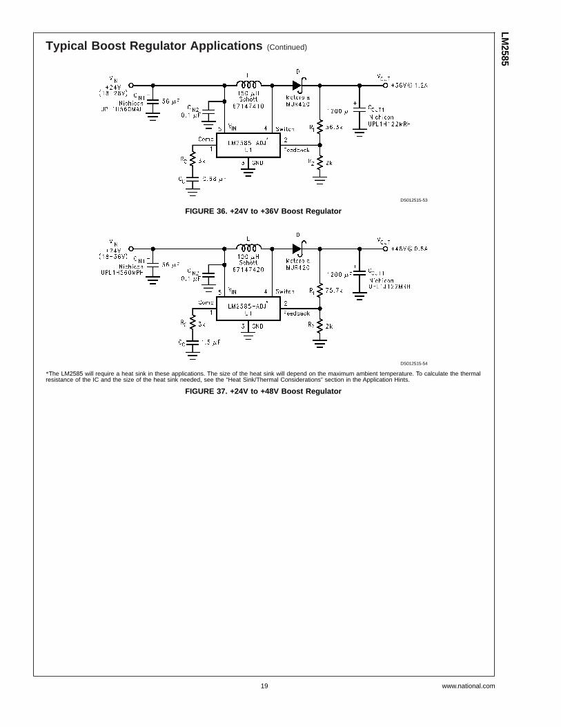
DS012515-53
FIGURE 36. +24V to +36V Boost Regulator
DS012515-54
*The LM2585 will require a heat sink in these applications. The size of the heat sink will depend on the maximum ambient temperature. To calculate the thermalresistance of the IC and the size of the heat sink needed, see the “Heat Sink/Thermal Considerations” section in the Application Hints.
FIGURE 37. +24V to +48V Boost Regulator
LM2585
www.national.com19

Application Hints
PROGRAMMING OUTPUT VOLTAGE(SELECTING R1 AND R2)
Referring to the adjustable regulator in Figure 38, the outputvoltage is programmed by the resistors R1 and R2 by thefollowing formula:
VOUT = VREF (1 + R1/R2) where VREF = 1.23V
Resistors R1 and R2 divide the output voltage down so thatit can be compared with the 1.23V internal reference. WithR2 between 1k and 5k, R1 is:
R1 = R2 (VOUT/VREF − 1) where VREF = 1.23V
For best temperature coefficient and stability with time, use1% metal film resistors.
SHORT CIRCUIT CONDITION
Due to the inherent nature of boost regulators, when theoutput is shorted (see Figure 38), current flows directly fromthe input, through the inductor and the diode, to the output,
bypassing the switch. The current limit of the switch does notlimit the output current for the entire circuit. To protect theload and prevent damage to the switch, the current must beexternally limited, either by the input supply or at the outputwith an external current limit circuit. The external limit shouldbe set to the maximum switch current of the device, which is3A.
In a flyback regulator application (Figure 39), using the stan-dard transformers, the LM2585 will survive a short circuit tothe main output. When the output voltage drops to 80% of itsnominal value, the frequency will drop to 25 kHz. With alower frequency, off times are larger. With the longer offtimes, the transformer can release all of its stored energybefore the switch turns back on. Hence, the switch turns oninitially with zero current at its collector. In this condition, theswitch current limit will limit the peak current, saving thedevice.
DS012515-55
FIGURE 38. Boost Regulator
DS012515-56
FIGURE 39. Flyback Regulator
LM25
85
www.national.com 20
Application Hints (Continued)
FLYBACK REGULATOR INPUT CAPACITORS
A flyback regulator draws discontinuous pulses of currentfrom the input supply. Therefore, there are two input capaci-tors needed in a flyback regulator; one for energy storageand one for filtering (see Figure 39). Both are required due tothe inherent operation of a flyback regulator. To keep astable or constant voltage supply to the LM2585, a storagecapacitor (≥100 µF) is required. If the input source is arectified DC supply and/or the application has a wide tem-perature range, the required rms current rating of the capaci-tor might be very large. This means a larger value of capaci-tance or a higher voltage rating will be needed of the inputcapacitor. The storage capacitor will also attenuate noisewhich may interfere with other circuits connected to thesame input supply voltage.
In addition, a small bypass capacitor is required due to thenoise generated by the input current pulses. To eliminate thenoise, insert a 1.0 µF ceramic capacitor between VIN andground as close as possible to the device.
SWITCH VOLTAGE LIMITS
In a flyback regulator, the maximum steady-state voltageappearing at the switch, when it is off, is set by the trans-former turns ratio, N, the output voltage, VOUT, and themaximum input voltage, VIN (Max):
VSW(OFF) = VIN (Max) + (VOUT +VF)/N
where VF is the forward biased voltage of the output diode,and is 0.5V for Schottky diodes and 0.8V for ultra-fast recov-ery diodes (typically). In certain circuits, there exists a volt-age spike, VLL, superimposed on top of the steady-statevoltage (see Figure 5, waveform A). Usually, this voltagespike is caused by the transformer leakage inductanceand/or the output rectifier recovery time. To “clamp” thevoltage at the switch from exceeding its maximum value, atransient suppressor in series with a diode is inserted acrossthe transformer primary (as shown in the circuit on the frontpage and other flyback regulator circuits throughout thedatasheet). The schematic in Figure 39 shows anothermethod of clamping the switch voltage. A single voltagetransient suppressor (the SA51A) is inserted at the switchpin. This method clamps the total voltage across the switch,not just the voltage across the primary.
If poor circuit layout techniques are used (see the “CircuitLayout Guideline” section), negative voltage transients mayappear on the Switch pin (pin 4). Applying a negative voltage(with respect to the IC’s ground) to any monolithic IC pincauses erratic and unpredictable operation of that IC. Thisholds true for the LM2585 IC as well. When used in a flybackregulator, the voltage at the Switch pin (pin 4) can go nega-tive when the switch turns on. The “ringing” voltage at theswitch pin is caused by the output diode capacitance and thetransformer leakage inductance forming a resonant circuit atthe secondary(ies). The resonant circuit generates the “ring-ing” voltage, which gets reflected back through the trans-former to the switch pin. There are two common methods toavoid this problem. One is to add an RC snubber around theoutput rectifier(s), as in Figure 39. The values of the resistorand the capacitor must be chosen so that the voltage at theSwitch pin does not drop below −0.4V. The resistor mayrange in value between 10Ω and 1 kΩ, and the capacitor willvary from 0.001 µF to 0.1 µF. Adding a snubber will (slightly)reduce the efficiency of the overall circuit.
The other method to reduce or eliminate the “ringing” is toinsert a Schottky diode clamp between pins 4 and 3
(ground), also shown in Figure 39. This prevents the voltageat pin 4 from dropping below −0.4V. The reverse voltagerating of the diode must be greater than the switch offvoltage.
OUTPUT VOLTAGE LIMITATIONS
The maximum output voltage of a boost regulator is themaximum switch voltage minus a diode drop. In a flybackregulator, the maximum output voltage is determined by theturns ratio, N, and the duty cycle, D, by the equation:
VOUT ≈ N x VIN x D/(1 − D)
The duty cycle of a flyback regulator is determined by thefollowing equation:
Theoretically, the maximum output voltage can be as largeas desired — just keep increasing the turns ratio of the trans-former. However, there exists some physical limitations thatprevent the turns ratio, and thus the output voltage, fromincreasing to infinity. The physical limitations are capaci-tances and inductances in the LM2585 switch, the outputdiode(s), and the transformer — such as reverse recoverytime of the output diode (mentioned above).
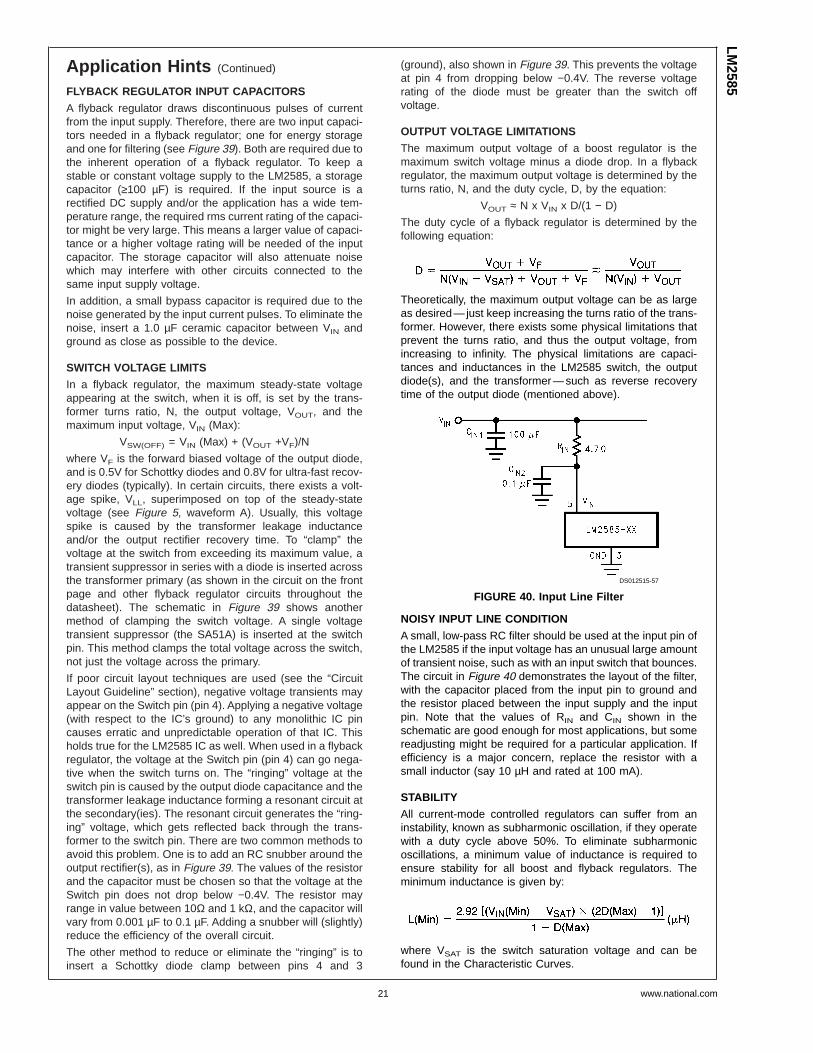
NOISY INPUT LINE CONDITION
A small, low-pass RC filter should be used at the input pin ofthe LM2585 if the input voltage has an unusual large amountof transient noise, such as with an input switch that bounces.The circuit in Figure 40 demonstrates the layout of the filter,with the capacitor placed from the input pin to ground andthe resistor placed between the input supply and the inputpin. Note that the values of RIN and CIN shown in theschematic are good enough for most applications, but somereadjusting might be required for a particular application. Ifefficiency is a major concern, replace the resistor with asmall inductor (say 10 µH and rated at 100 mA).
STABILITY
All current-mode controlled regulators can suffer from aninstability, known as subharmonic oscillation, if they operatewith a duty cycle above 50%. To eliminate subharmonicoscillations, a minimum value of inductance is required toensure stability for all boost and flyback regulators. Theminimum inductance is given by:
where VSAT is the switch saturation voltage and can befound in the Characteristic Curves.
DS012515-57
FIGURE 40. Input Line Filter
LM2585
www.national.com21

Application Hints (Continued)
CIRCUIT LAYOUT GUIDELINES
As in any switching regulator, layout is very important. Rap-idly switching currents associated with wiring inductancegenerate voltage transients which can cause problems. Forminimal inductance and ground loops, keep the length of theleads and traces as short as possible. Use single pointgrounding or ground plane construction for best results.Separate the signal grounds from the power grounds (asindicated in Figure 41). When using the Adjustable version,physically locate the programming resistors as near theregulator IC as possible, to keep the sensitive feedbackwiring short.
HEAT SINK/THERMAL CONSIDERATIONS
In many cases, no heat sink is required to keep the LM2585junction temperature within the allowed operating range. Foreach application, to determine whether or not a heat sink willbe required, the following must be identified:
1) Maximum ambient temperature (in the application).
2) Maximum regulator power dissipation (in the application).
3) Maximum allowed junction temperature (125˚C for theLM2585). For a safe, conservative design, a temperatureapproximately 15˚C cooler than the maximum junction tem-perature should be selected (110˚C).
4) LM2585 package thermal resistances θJA and θJC (givenin the Electrical Characteristics).
Total power dissipated (PD) by the LM2585 can be estimatedas follows:
VIN is the minimum input voltage, VOUT is the output voltage,N is the transformer turns ratio, D is the duty cycle, and ILOAD
is the maximum load current (and ∑ILOAD is the sum of themaximum load currents for multiple-output flyback regula-tors). The duty cycle is given by:
where VF is the forward biased voltage of the diode and istypically 0.5V for Schottky diodes and 0.8V for fast recoverydiodes. VSAT is the switch saturation voltage and can befound in the Characteristic Curves.
When no heat sink is used, the junction temperature rise is:
∆TJ = PD x θJA.
Adding the junction temperature rise to the maximum ambi-ent temperature gives the actual operating junction tempera-ture:
TJ = ∆TJ + TA.
If the operating junction temperature exceeds the maximumjunction temperatue in item 3 above, then a heat sink isrequired. When using a heat sink, the junction temperaturerise can be determined by the following:
∆TJ = PD x (θJC + θInterface + θHeat Sink)
Again, the operating junction temperature will be:
TJ = ∆TJ + TA
As before, if the maximum junction temperature is exceeded,a larger heat sink is required (one that has a lower thermalresistance).
Included in the Switchers Made Simple design software isa more precise (non-linear) thermal model that can be usedto determine junction temperature with different input-outputparameters or different component values. It can also calcu-late the heat sink thermal resistance required to maintain theregulator junction temperature below the maximum operat-ing temperature.
To further simplify the flyback regulator design procedure,National Semiconductor is making available computer de-sign software to be used with the Simple Switcher line ofswitching regulators. Switchers Made Simple is availableon a 31⁄2" diskette for IBM compatible computers from aNational Semiconductor sales office in your area or theNational Semiconductor Customer Response Center(1-800-272-9959).
DS012515-58
FIGURE 41. Circuit Board Layout
LM25
85
www.national.com 22

European Magnetic VendorContactsPlease contact the following addresses for details of localdistributors or representatives:
Coilcraft21 Napier Place
Wardpark North
Cumbernauld, Scotland G68 0LL
Phone: +44 1236 730 595
Fax: +44 1236 730 627
Pulse EngineeringDunmore Road
Tuam
Co. Galway, Ireland
Phone: +353 93 24 107
Fax: +353 93 24 459
LM2585
www.national.com23

Physical Dimensions inches (millimeters) unless otherwise noted
Order Number LM2585T-3.3, LM2585T-5.0,LM2585T-12 or LM2585T-ADJ
NS Package Number T05D
LM25
85
www.national.com 24

Physical Dimensions inches (millimeters) unless otherwise noted (Continued)
LIFE SUPPORT POLICY
NATIONAL’S PRODUCTS ARE NOT AUTHORIZED FOR USE AS CRITICAL COMPONENTS IN LIFE SUPPORTDEVICES OR SYSTEMS WITHOUT THE EXPRESS WRITTEN APPROVAL OF THE PRESIDENT AND GENERALCOUNSEL OF NATIONAL SEMICONDUCTOR CORPORATION. As used herein:
1. Life support devices or systems are devices orsystems which, (a) are intended for surgical implantinto the body, or (b) support or sustain life, andwhose failure to perform when properly used inaccordance with instructions for use provided in thelabeling, can be reasonably expected to result in asignificant injury to the user.
2. A critical component is any component of a lifesupport device or system whose failure to performcan be reasonably expected to cause the failure ofthe life support device or system, or to affect itssafety or effectiveness.
National SemiconductorCorporationAmericasEmail: [email protected]
National SemiconductorEurope
Fax: +49 (0) 180-530 85 86Email: [email protected]
Deutsch Tel: +49 (0) 69 9508 6208English Tel: +44 (0) 870 24 0 2171Français Tel: +33 (0) 1 41 91 8790
National SemiconductorAsia Pacific CustomerResponse GroupTel: 65-2544466Fax: 65-2504466Email: [email protected]
National SemiconductorJapan Ltd.Tel: 81-3-5639-7560Fax: 81-3-5639-7507
www.national.com
Order Number LM2585S-3.3, LM2585S-5.0,LM2585S-12 or LM2585S-ADJ
NS Package Number TS5B
LM2585
SIM
PLE
SW
ITCH
ER
3AFlyback
Regulator
National does not assume any responsibility for use of any circuitry described, no circuit patent licenses are implied and National reserves the right at any time without notice to change said circuitry and specifications.