lm1086 1.5a low dropout positive regulators (rev. …...• battery charger • post regulation for...
TRANSCRIPT

VIN
N/C
N/C
VOUT
1
3
4
2
6
5
7
8ADJ/GND
N/C
VOUT
VOUT
VOUT
LM1086LM1086 1.5A Low Dropout Positive Regulators
1FEATURES DESCRIPTIONThe LM1086 is a series of low dropout positive
2• Available in 1.8V, 2.5V, 2.85V, 3.3V, 3.45V, 5Vvoltage regulators with a maximum dropout of 1.5V atand Adjustable Versions1.5A of load current. It has the same pin-out as TI's
• Current Limiting and Thermal Protection industry standard LM317.• Output Current 1.5A
The LM1086 is available in an adjustable version,• Line Regulation 0.015% (typical) which can set the output voltage with only two
external resistors. It is also available in six fixed• Load Regulation 0.1% (typical)voltages: 1.8V, 2.5V, 2.85V, 3.3V, 3.45V and 5.0V.The fixed versions integrate the adjust resistors.APPLICATIONSThe LM1086 circuit includes a zener trimmed• SCSI-2 Active Terminatorbandgap reference, current limiting and thermal• High Efficiency Linear Regulatorsshutdown.
• Battery Charger• Post Regulation for Switching Supplies• Constant Current Regulator• Microprocessor Supply
Connection Diagram
Pins 6, 7, and 8 must be tied together.
Figure 1. TO-220 Figure 2. DDPAK/TO-263 Figure 3. WSONTop View Top View Top View
Figure 4. Basic Functional Diagram, Figure 5. Application CircuitAdjustable Version 1.2V to 15V Adjustable Regulator

Simplified SchematicLM1086

These devices have limited built-in ESD protection. The leads should be shorted together or the device placed in conductive foamduring storage or handling to prevent electrostatic damage to the MOS gates.
Absolute Maximum Ratings (1) (2)
Maximum Input-to-Output Voltage Differential
LM1086-ADJ 29V
LM1086-1.8 27V
LM1086-2.5 27V
LM1086-2.85 27V
LM1086-3.3 27V
LM1086-3.45 27V
LM1086-5.0 25V
Power Dissipation (3) Internally Limited
Junction Temperature (TJ)(4) 150°C
Storage Temperature Range -65°C to 150°C
Lead Temperature 260°C, to 10 sec
ESD Tolerance (5) 2000V
(1) Absolute Maximum Ratings indicate limits beyond which damage to the device may occur. Operating Ratings indicate conditions forwhich the device is intended to be functional, but specific performance is not ensured. For ensured specifications and the testconditions, see the Electrical Characteristics.
(2) If Military/Aerospace specified devices are required, please contact the Texas Instruments Sales Office/Distributors for availability andspecifications.
(3) Power dissipation is kept in a safe range by current limiting circuitry. Refer to OVERLOAD RECOVERY in Application Note. The valueθJA for the WSON package is specifically dependent on PCB trace area, trace material, and the number of thermal vias. For improvedthermal resistance and power dissipation for the WSON package, refer to Application Note AN-1187 (literature number SNOA401).
(4) The maximum power dissipation is a function of TJ(MAX) , θJA, and TA. The maximum allowable power dissipation at any ambienttemperature is PD = (TJ(MAX)–T A)/θJA. All numbers apply for packages soldered directly into a PC board. Refer to ThermalConsiderations in the Application Notes.
(5) For testing purposes, ESD was applied using human body model, 1.5kΩ in series with 100pF.
Operating Ratings (1)
Junction Temperature Range (TJ)(2)
Control Section 0°C to 125°C
"C" Grade Output Section 0°C to 150°C
Control Section −40°C to 125°C
"I" Grade Output Section −40°C to 150°C
(1) Absolute Maximum Ratings indicate limits beyond which damage to the device may occur. Operating Ratings indicate conditions forwhich the device is intended to be functional, but specific performance is not ensured. For ensured specifications and the testconditions, see the Electrical Characteristics.
(2) The maximum power dissipation is a function of TJ(MAX) , θJA, and TA. The maximum allowable power dissipation at any ambienttemperature is PD = (TJ(MAX)–T A)/θJA. All numbers apply for packages soldered directly into a PC board. Refer to ThermalConsiderations in the Application Notes.
LM1086
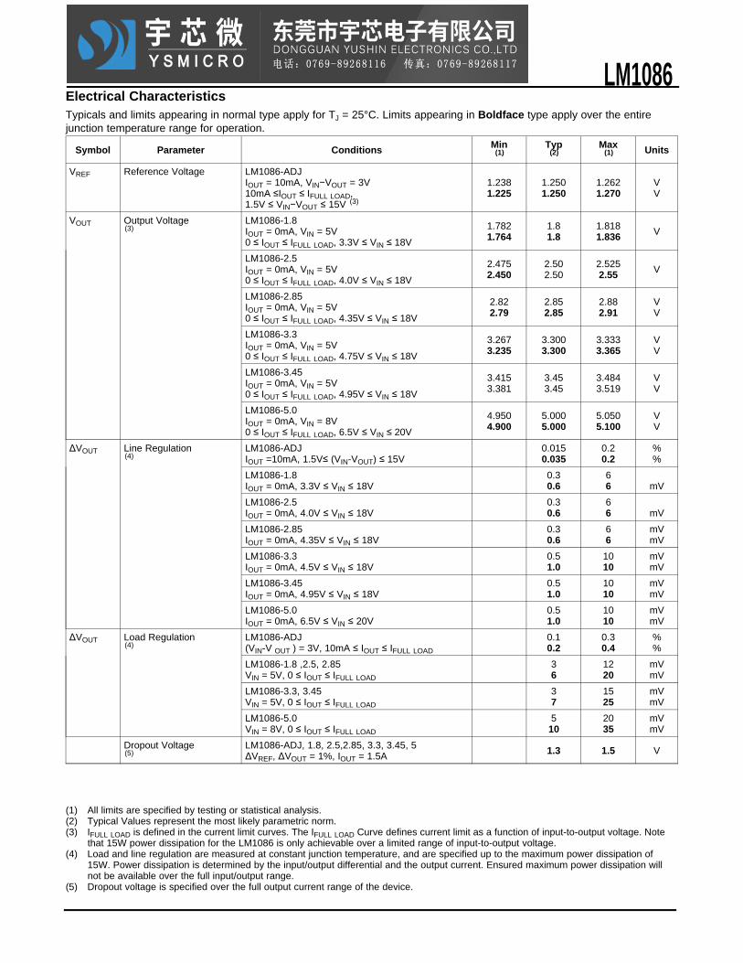
Electrical CharacteristicsTypicals and limits appearing in normal type apply for TJ = 25°C. Limits appearing in Boldface type apply over the entirejunction temperature range for operation.
Min Typ MaxSymbol Parameter Conditions Units(1) (2) (1)
VREF Reference Voltage LM1086-ADJIOUT = 10mA, VIN−VOUT = 3V 1.238 1.250 1.262 V10mA ≤IOUT ≤ IFULL LOAD, 1.225 1.250 1.270 V1.5V ≤ VIN−VOUT ≤ 15V (3)
VOUT Output Voltage LM1086-1.8 1.782 1.8 1.818(3) IOUT = 0mA, VIN = 5V V1.764 1.8 1.8360 ≤ IOUT ≤ IFULL LOAD, 3.3V ≤ VIN ≤ 18V
LM1086-2.5 2.475 2.50 2.525IOUT = 0mA, VIN = 5V V2.450 2.50 2.550 ≤ IOUT ≤ IFULL LOAD, 4.0V ≤ VIN ≤ 18V
LM1086-2.85 2.82 2.85 2.88 VIOUT = 0mA, VIN = 5V 2.79 2.85 2.91 V0 ≤ IOUT ≤ IFULL LOAD, 4.35V ≤ VIN ≤ 18V
LM1086-3.3 3.267 3.300 3.333 VIOUT = 0mA, VIN = 5V 3.235 3.300 3.365 V0 ≤ IOUT ≤ IFULL LOAD, 4.75V ≤ VIN ≤ 18V
LM1086-3.45 3.415 3.45 3.484 VIOUT = 0mA, VIN = 5V 3.381 3.45 3.519 V0 ≤ IOUT ≤ IFULL LOAD, 4.95V ≤ VIN ≤ 18V
LM1086-5.0 4.950 5.000 5.050 VIOUT = 0mA, VIN = 8V 4.900 5.000 5.100 V0 ≤ IOUT ≤ IFULL LOAD, 6.5V ≤ VIN ≤ 20V
ΔVOUT Line Regulation LM1086-ADJ 0.015 0.2 %(4) IOUT =10mA, 1.5V≤ (VIN-VOUT) ≤ 15V 0.035 0.2 %
LM1086-1.8 0.3 6IOUT = 0mA, 3.3V ≤ VIN ≤ 18V 0.6 6 mV
LM1086-2.5 0.3 6IOUT = 0mA, 4.0V ≤ VIN ≤ 18V 0.6 6 mV
LM1086-2.85 0.3 6 mVIOUT = 0mA, 4.35V ≤ VIN ≤ 18V 0.6 6 mV
LM1086-3.3 0.5 10 mVIOUT = 0mA, 4.5V ≤ VIN ≤ 18V 1.0 10 mV
LM1086-3.45 0.5 10 mVIOUT = 0mA, 4.95V ≤ VIN ≤ 18V 1.0 10 mV
LM1086-5.0 0.5 10 mVIOUT = 0mA, 6.5V ≤ VIN ≤ 20V 1.0 10 mV
ΔVOUT Load Regulation LM1086-ADJ 0.1 0.3 %(4) (VIN-V OUT ) = 3V, 10mA ≤ IOUT ≤ IFULL LOAD 0.2 0.4 %
LM1086-1.8 ,2.5, 2.85 3 12 mVVIN = 5V, 0 ≤ IOUT ≤ IFULL LOAD 6 20 mV
LM1086-3.3, 3.45 3 15 mVVIN = 5V, 0 ≤ IOUT ≤ IFULL LOAD 7 25 mV
LM1086-5.0 5 20 mVVIN = 8V, 0 ≤ IOUT ≤ IFULL LOAD 10 35 mV
Dropout Voltage LM1086-ADJ, 1.8, 2.5,2.85, 3.3, 3.45, 5 1.3 1.5 V(5) ΔVREF, ΔVOUT = 1%, IOUT = 1.5A
(1) All limits are specified by testing or statistical analysis.(2) Typical Values represent the most likely parametric norm.(3) IFULL LOAD is defined in the current limit curves. The IFULL LOAD Curve defines current limit as a function of input-to-output voltage. Note
that 15W power dissipation for the LM1086 is only achievable over a limited range of input-to-output voltage.(4) Load and line regulation are measured at constant junction temperature, and are specified up to the maximum power dissipation of
15W. Power dissipation is determined by the input/output differential and the output current. Ensured maximum power dissipation willnot be available over the full input/output range.
(5) Dropout voltage is specified over the full output current range of the device.
LM1086

Electrical Characteristics (continued)Typicals and limits appearing in normal type apply for TJ = 25°C. Limits appearing in Boldface type apply over the entirejunction temperature range for operation.
Min Typ MaxSymbol Parameter Conditions Units(1) (2) (1)
ILIMIT Current Limit LM1086-ADJVIN−VOUT = 5V 1.50 2.7 AVIN−VOUT = 25V 0.05 0.15 A
LM1086-1.8,2.5, 2.85, 3.3, 3.45, VIN = 8V 1.5 2.7 A
LM1086-5.0, VIN = 10V 1.5 2.7 A
Minimum Load Current (6) LM1086-ADJVIN −VOUT = 25V 5.0 10.0 mA
Quiescent Current LM1086-1.8, 2.5, 2.85, VIN ≤ 18V 5.0 10.0 mA
LM1086-3.3, VIN ≤ 18V 5.0 10.0 mA
LM1086-3.45, VIN ≤ 18V 5.0 10.0 mA
LM1086-5.0, VIN ≤ 20V 5.0 10.0 mA
Thermal Regulation TA = 25°C, 30ms Pulse 0.008 0.04 %/W
Ripple Rejection fRIPPLE = 120Hz, COUT = 25µF Tantalum,IOUT = 1.5A
LM1086-ADJ, CADJ = 25µF, (VIN−VO) = 3V 60 75 dB
LM1086-1.8, 2.5, 2.85, VIN = 6V 60 72 dB
LM1086-3.3, VIN= 6.3V 60 72 dB
LM1086-3.45, VIN= 6.3V 60 72 dB
LM1086-5.0 VIN = 8V 60 68 dB
Adjust Pin Current LM1086 55 120 µA
Adjust Pin Current 10mA ≤ IOUT ≤ IFULL LOAD,Change 1.5V ≤ (VIN−VOUT) ≤ 15V 0.2 5 µA
Temperature Stability 0.5 %
Long Term Stability TA = 125°C, 1000Hrs 0.3 1.0 %
RMS Noise 10Hz ≤ f≤ 10kHz 0.003 %(% of VOUT)
θJC Thermal Resistance 3-Lead DDPAK/TO-263: Control Section/Output 1.5/4.0 °C/WJunction-to-Case Section 1.5/4.0 °C/W
3-Lead TO-220: Control Section/Output Section
(6) The minimum output current required to maintain regulation.
LM1086

Typical Performance Characteristics
Dropout Voltage vs. Output Current Short-Circuit Current vs. Input/Output Difference
Figure 6. Figure 7.
Load Regulation vs. Temperature Percent Change in Output Voltage vs. Temperature
Figure 8. Figure 9.
Adjust Pin Current vs. Temperature Maximum Power Dissipation vs. Temperature
Figure 10. Figure 11.
LM1086

Typical Performance Characteristics (continued)Ripple Rejection vs. Frequency (LM1086-Adj.) Ripple Rejection vs. Output Current (LM1086-Adj.)
Figure 12. Figure 13.
Ripple Rejection vs. Frequency (LM1086-5) Ripple Rejection vs. Output Current (LM1086-5)
Figure 14. Figure 15.
Line Transient Response Load Transient Response
Figure 16. Figure 17.
LM1086

GENERAL
Figure 18 shows a basic functional diagram for the LM1086-Adj (excluding protection circuitry) . The topology isbasically that of the LM317 except for the pass transistor. Instead of a Darlingtion NPN with its two diode voltagedrop, the LM1086 uses a single NPN. This results in a lower dropout voltage. The structure of the pass transistoris also known as a quasi LDO. The advantage a quasi LDO over a PNP LDO is its inherently lower quiescentcurrent. The LM1086 is specified to provide a minimum dropout voltage 1.5V over temperature, at full load.
Figure 18. Basic Functional Diagram for the LM1086, excluding Protection circuitry
OUTPUT VOLTAGE
The LM1086 adjustable version develops at 1.25V reference voltage, (VREF), between the output and the adjustterminal. As shown in figure 2, this voltage is applied across resistor R1 to generate a constant current I1. Thisconstant current then flows through R2. The resulting voltage drop across R2 adds to the reference voltage tosets the desired output voltage.
The current IADJ from the adjustment terminal introduces an output error . But since it is small (120uA max), itbecomes negligible when R1 is in the 100Ω range.
For fixed voltage devices, R1 and R2 are integrated inside the devices.
Figure 19. Basic Adjustable Regulator
STABILITY CONSIDERATION
Stability consideration primarily concern the phase response of the feedback loop. In order for stable operation,the loop must maintain negative feedback. The LM1086 requires a certain amount series resistance withcapacitive loads. This series resistance introduces a zero within the loop to increase phase margin and thusincrease stability. The equivalent series resistance (ESR) of solid tantalum or aluminum electrolytic capacitors isused to provide the appropriate zero (approximately 500 kHz).
LM1086

The Aluminum electrolytic are less expensive than tantalums, but their ESR varies exponentially at coldtemperatures; therefore requiring close examination when choosing the desired transient response overtemperature. Tantalums are a convenient choice because their ESR varies less than 2:1 over temperature.
The recommended load/decoupling capacitance is a 10uF tantalum or a 50uF aluminum. These values willassure stability for the majority of applications.
The adjustable versions allows an additional capacitor to be used at the ADJ pin to increase ripple rejection. Ifthis is done the output capacitor should be increased to 22uF for tantalums or to 150uF for aluminum.
Capacitors other than tantalum or aluminum can be used at the adjust pin and the input pin. A 10uF capacitor isa reasonable value at the input. See RIPPLE REJECTION section regarding the value for the adjust pincapacitor.
It is desirable to have large output capacitance for applications that entail large changes in load current(microprocessors for example). The higher the capacitance, the larger the available charge per demand. It is alsodesirable to provide low ESR to reduce the change in output voltage:
ΔV = ΔI x ESR
It is common practice to use several tantalum and ceramic capacitors in parallel to reduce this change in theoutput voltage by reducing the overall ESR.
Output capacitance can be increased indefinitely to improve transient response and stability.
RIPPLE REJECTION
Ripple rejection is a function of the open loop gain within the feed-back loop (refer to Figure 18 and Figure 19).The LM1086 exhibits 75dB of ripple rejection (typ.). When adjusted for voltages higher than VREF, the ripplerejection decreases as function of adjustment gain: (1+R1/R2) or VO/VREF. Therefore a 5V adjustment decreasesripple rejection by a factor of four (−12dB); Output ripple increases as adjustment voltage increases.
However, the adjustable version allows this degradation of ripple rejection to be compensated. The adjustterminal can be bypassed to ground with a capacitor (CADJ). The impedance of the CADJ should be equal to orless than R1 at the desired ripple frequency. This bypass capacitor prevents ripple from being amplified as theoutput voltage is increased.
1/(2π*fRIPPLE*CADJ) ≤ R1
LOAD REGULATION
The LM1086 regulates the voltage that appears between its output and ground pins, or between its output andadjust pins. In some cases, line resistances can introduce errors to the voltage across the load. To obtain thebest load regulation, a few precautions are needed.
Figure 20 shows a typical application using a fixed output regulator. Rt1 and Rt2 are the line resistances. VLOADis less than the VOUT by the sum of the voltage drops along the line resistances. In this case, the load regulationseen at the RLOAD would be degraded from the data sheet specification. To improve this, the load should be tieddirectly to the output terminal on the positive side and directly tied to the ground terminal on the negative side.
Figure 20. Typical Application using Fixed Output Regulator
LM1086

When the adjustable regulator is used (Figure 21), the best performance is obtained with the positive side of theresistor R1 tied directly to the output terminal of the regulator rather than near the load. This eliminates line dropsfrom appearing effectively in series with the reference and degrading regulation. For example, a 5V regulator with0.05Ω resistance between the regulator and load will have a load regulation due to line resistance of 0.05Ω x IL.If R1 (=125Ω) is connected near the load the effective line resistance will be 0.05Ω (1 + R2/R1) or in this case, itis 4 times worse. In addition, the ground side of the resistor R2 can be returned near the ground of the load toprovide remote ground sensing and improve load regulation.
Figure 21. Best Load Regulation using Adjustable Output Regulator
PROTECTION DIODES
Under normal operation, the LM1086 regulator does not need any protection diode. With the adjustable device,the internal resistance between the adjustment and output terminals limits the current. No diode is needed todivert the current around the regulator even with a capacitor on the adjustment terminal. The adjust pin can takea transient signal of ±25V with respect to the output voltage without damaging the device.
When an output capacitor is connected to a regulator and the input is shorted, the output capacitor will dischargeinto the output of the regulator. The discharge current depends on the value of the capacitor, the output voltageof the regulator, and rate of decrease of VIN. In the LM1086 regulator, the internal diode between the output andinput pins can withstand microsecond surge currents of 10A to 20A. With an extremely large output capacitor(≥1000 µf), and with input instantaneously shorted to ground, the regulator could be damaged. In this case, anexternal diode is recommended between the output and input pins to protect the regulator, shown in Figure 22.
Figure 22. Regulator with Protection Diode
LM1086
OVERLOAD RECOVERY
Overload recovery refers to regulator's ability to recover from a short circuited output. A key factor in the recoveryprocess is the current limiting used to protect the output from drawing too much power. The current limiting circuitreduces the output current as the input to output differential increases. Refer to short circuit curve in the TypicalPerformance Characteristics section.
During normal start-up, the input to output differential is small since the output follows the input. But, if the outputis shorted, then the recovery involves a large input to output differential. Sometimes during this condition thecurrent limiting circuit is slow in recovering. If the limited current is too low to develop a voltage at the output, thevoltage will stabilize at a lower level. Under these conditions it may be necessary to recycle the power of theregulator in order to get the smaller differential voltage and thus adequate start up conditions. Refer to TypicalPerformance Characteristics section for the short circuit current vs. input differential voltage.
THERMAL CONSIDERATIONS
ICs heats up when in operation, and power consumption is one factor in how hot it gets. The other factor is howwell the heat is dissipated. Heat dissipation is predictable by knowing the thermal resistance between the IC andambient (θJA). Thermal resistance has units of temperature per power (C/W). The higher the thermal resistance,the hotter the IC.
The LM1086 specifies the thermal resistance for each package as junction to case (θJC). In order to get the totalresistance to ambient (θJA), two other thermal resistance must be added, one for case to heat-sink (θCH) and onefor heatsink to ambient (θHA). The junction temperature can be predicted as follows:
TJ = TA + PD (θJC + θCH + θHA) = TA + PD θJA
where• TJ is junction temperature• TA is ambient temperature• PD is the power consumption of the device
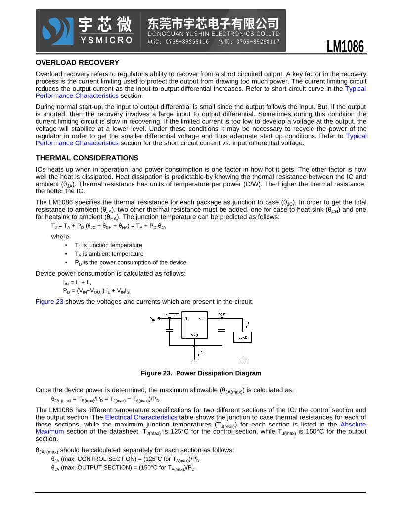
Device power consumption is calculated as follows:IIN = IL + IGPD = (VIN−VOUT) IL + VINIG
Figure 23 shows the voltages and currents which are present in the circuit.
Figure 23. Power Dissipation Diagram
Once the device power is determined, the maximum allowable (θJA(max)) is calculated as:θJA (max) = TR(max)/PD = TJ(max) − TA(max))/PD
The LM1086 has different temperature specifications for two different sections of the IC: the control section andthe output section. The Electrical Characteristics table shows the junction to case thermal resistances for each ofthese sections, while the maximum junction temperatures (TJ(max)) for each section is listed in the AbsoluteMaximum section of the datasheet. TJ(max) is 125°C for the control section, while TJ(max) is 150°C for the outputsection.
θJA (max) should be calculated separately for each section as follows:θJA (max, CONTROL SECTION) = (125°C for TA(max))/PD
θJA (max, OUTPUT SECTION) = (150°C for TA(max))/PD
LM1086

The required heat sink is determined by calculating its required thermal resistance (θHA(max)).θHA(max) = θJA(max) − (θJC + θCH)
θHA (max) should be calculated twice as follows:θHA (max) = θJA(max, CONTROL SECTION) - (θJC (CONTROL SECTION) + θCH)θHA (max)= θJA(max, OUTPUT SECTION) - (θJC(OUTPUT SECTION) + θCH)
If thermal compound is used, θCH can be estimated at 0.2 C/W. If the case is soldered to the heat sink, then aθCH can be estimated as 0 C/W.
After, θHA (max) is calculated for each section, choose the lower of the two θHA (max) values to determine theappropriate heat sink.
If PC board copper is going to be used as a heat sink, then Figure 24 can be used to determine the appropriatearea (size) of copper foil required.
Figure 24. Heat sink thermal Resistance vs. Area
Typical Applications
Figure 25. 5V to 3.3V, 1.5A Regulator Figure 26. Adjustable @ 5V
LM1086

Figure 27. 1.2V to 15V Adjustable Regulator Figure 28. 5V Regulator with Shutdown
Figure 29. Battery Charger Figure 30. Adjustable Fixed Regulator
Figure 31. Regulator with Reference Figure 32. High Current Lamp Driver Protection
Figure 33. Battery Backup Regulated Supply Figure 34. Ripple Rejection Enhancement
LM1086

Figure 35. Automatic Light control
Figure 36. Remote Sensing
Figure 37. SCSI-2 Active termination
LM1086