ll 0 i - defense technical information center of contents i introduction i 11 theory of the solar...
TRANSCRIPT

s 7/.)tCT~T
41O~GTP 0
Ll 0 i
LA0

11 SA J-
YOUR KEY... c
0 0
CLEARINGHOUSEFOR FEDERAL SCIENTIFIC AND TECHNICAL INFORMATION ij
to scientific and technical advancementMr. Scientist. . .Engineer. . .Businessman. . .the Clearinghouse for Scientific and Tech-
nical Information can serve as your key to progress in research and development. Eachyear, some 40,000 unclassified documents from more than 125 Government agencies en-ter our collection. The Clearinghouse announces, reproduces and sells these reports tothe public at a nominal cost. To make this wealth of scientific and technical informa-tion readily available, we have tailored our services to meet the needs of the highly se-lective customer as well as the general user. Some of these services are listed below.
U.S. GOVERNMENT RESEARCH AND DEVELOPMENT REPORTS (USGRDR). This semimonthlyjournal abstracts approximately 40,000 new Government- sponsored reports and translations an-n ually. Features a quick-scan format, cross references, edge index to subject fields, and a re- 0porf ': tor list.
U.S. GOVERNMEN1 RESEARCH AND DEVELOPMENT REPORTS INDEX (USGRDR-I). Publish-ed concurrently with the USGIRDR to index each issue by subject, personal author, corporatesource, contract number and accession 'report number. Quarterly Indexes and an Annual Cumu-lative also are avail.ble.
CLEARINGHOUSE ANNOUNCEMENTS IN SCIENCE AND TECHNOLOGY. A semimonthly current 0awareness announcement service in 46 separate categories representing complete coverage ofall documents announced by the Clearinghouse. Highlights special interest reports.
FAST ANNOUNCEMENT SERVICE (FAS). Selective announcement service emphasizing commer-cial applications of report information. Covers approximately 10 percent of Clearinghousedocument input. Compiled and mailed in 57 categories.
SELECTIVE DISSEMINATION OF MICROFICHE (SDM). Automatic distribution twice monthly ofGovernment research and development reports on microfiche. Economical and highly selec-tive. Several hundred categories from which to choose.
ADDITIONAL INFORMATION concerning these and other Clearinghouse services is available bywriting to:
Customer ServicesClearinghouseU.S. Department of CommerceSpringfield, Virginia 22151
•

HANDB3/r.
'7-' 7-
COO 1,1Y A N[D) JAN1) A
-AN[)
a74., 0
X S
N A IO A A£O A T C A ND. S P A E A D M I IS T R TIO

NASA SP-3003
0
By William C. Cooley and Robert J. Janda
Prepared under contract for NASA by Exotech, Incorporated,Alexandria, Virginia. and reproduced
photographicaily from copy supplied by the
contractor
0
m Offie of S, intifi(' and re~ ,hnic,,I nf,,rmation 1963NATIONAL AERONAUTICS AND SPACE ADMINISTRATION
~Washingfton. D.C.
By William C. Cooley and R t J

0
ACKNOWLEDGEMENTS 0
The guidance of Walter C. Scott of National
Aeronautics and Space Administration Head-
quarters is gratefully acknowledged. Special
thanks are due Kandiah Sh'vanandan who served
as consultant to the authors. The cooperation 0
of many other individuals and organizations in
providing data is also acknowledged with thanks.
0
For Sale by the Office of Technical Services, Department of 0Commerce, Washington, D.C. 20230--Price $2. 50

0
FORBWORD
In order that photovoltaic solar cells may be used more effectively to
provide electrical power for spacecraft, it is desirable to refine the engineering
design of solar cells and power systems, based on a better understanding of the
space radiation environment and of radiation damage effects on semiconductor 0
components. The objective of this handbook is to provide a summary of some of
the useful analytical methods and test data which can be applied in designing
radiation resistant power systems. It is found that the most serious obstacle
which prevents accurate prediction of solar cell degradation for earth satellites 0
is our inadequate knowledge of the fluxes and energy spectra of electrons and
protons in the magnetosphere. When the space environment can be better defined,
it will be possible to predict more accurately the degradation of present day
types of silicon solar cells, for which the radiation damage characteristics
have been quite well determined by laboratory research. As improved types of
solar cells and materials become available, it will be necessary to make laboratory
measurements of their radiation resistance to protons and electrons in order to 0
predict their performance in space. Therefore, the performance data presented
herein may become obsolete. However, it is hoped that the methods for data
correlation and analysis presented here will be an aid to understanding the nature
of the problems involved, and will be useful in the conduct of engineering analysis. 0
o..111
h m || m - mr- ii i - . .

TABLE OF CONTENTS
I Introduction I
11 Theory of the Solar Cell 2
A. The Photovoltaic Effect 2 0
B. Solar Cell Design 3
C. Solar Cell Performance 5
Il Radiation Damage to Solar Cells 12
A. Production of Defects and Recombination Centers by Radiation 12 0
B. Simplifying Assumptions 13
C. Effect of Radiation on Diffusion Length 14
D. Electron Damage Coefficients 18
E. Proton Damage Coefficients 18
F. Calculation of the Diffusion Length From Laboratory Data 27
G. Correlation of the Performance of Solar Cells as a Function ofDiffusion Length 28
IV The Space Radiation Environment 44
A. Introduction 44
B. Mcllwain's Coordinates 44
C. Electron Fluxes and Energy Spectra 46
D. Proton Fluxes and Energy Spectra 51
V Correlation of Satellite Test Data on Solar Cell Performance 55
VI Design Methods for Solar Cell Power Systems 63
A. General Requirements 63 0
B. Selection of Type of Solar Cells 63
C. Degradation Rates in Particular Orbits as a Function of Shield Thickness 63
D. Calculation of Solar Cell Degradation Rates 64
E. Sample Calculation of Radiation Damage in Equatorial Orbits 65 0
F. Comparison of Calculated and Observed Damage on S-27 Alouette 74
- iv -

0
TABLE OF CONTENTS (CONT'D)
Appendix A. Radiation Effects on Solar Cell Cover Slide Materials and Adhesives A IA. Introduction Al
B. Damage Mechanism Al
C. Cover Slide Requirements A2
D. Electron and Proton Damage Experiments A 2
E. Conclusion A 14 0
Appendix B. Space Radiation Effects on Transistors and Diodes B I
A. Introduction B1
B. Radiation Damage Mechanisms BI
C. Surface Effects of Radiation BI 0
D. Degradation of Diffusion Length in Transistors B 2
E. Selection of Transistor Type B5
F. Diodes B 5
G. Shielding Against Space Radiation B6
References R I
0
0
0
0
0
LIST OF FIGURES
Figure
Number Page
I N on P Silicon Solar Cell 4
2 Typical Current-Voltage Characteristic for a Solar Cell 6
3A N/P Silicon Solar Cell Current Density as a Function of Diffusion Length 7
3 B P/N Silicon Solar Cell Current Density as a Function of Diffusion Length 8
4 Short Circuit Current Density vs. Diffusion Length for Two Light Sources 10 0
5 Maximum Power Output as a Function of Diffusion Length for N/P SolarCells in Space Sunlight 11
6A Diffusion Length Degradation of N/P Solar Cells With I MEV Electrons 15
6B Diffusion Length Degradation of P/N Solar Cells With 1 MEV Electrons 16 0
7 Degradation of Diffusion Length in I ohm-cm P-Type Silicon as aFunction of Integrated Flux 17
8 Electron Damage Coefficient as a Function of Electron Energy for N/PSilicon Cells 19
9 Electron Damage Coefficient as a Function of Electron Energy for P/NSilicon Cells 20
10 Effect of Electron Energy on Damage Rate for N/P and P/N Silicon Cells 21
11 Proton Damage Coefficient for N/P Silicon Cells as a Function of ProtonEnergy 25
12 Proton Damage Coefficient for P/N Silicon Cells as a Function of ProtonEnergy 26
13 Typical Spectral Response of RCA N/P (I ohm-cm).Solar Cell to 1.0 MEVElectrons 29
14 Current-Voltage Characteristic for BTL Blue-Shifted N/P Silicon SolarCell 31
15 Short Circuit Current Ratio vs. Diffusion Length Ratio For Silicon SolarCells 33
16 Degraded vs. Initial Diffusion Length For 75%0 Short Circuit Current InSilicon Solar Cells 34
17 Typical Variation of Maximum Power Ratio With Short Circuit CurrentRatio 36
- vi -
0
0
LIST OF FIGURES (CONT-D)
FigureNumber Page
18 Power vs. Voltage at Various Stages of Degradation For Blue N/P1 Ohm-cm BTL Silicon Cells 37
19 Maximum Power Ratio vs. Diffusion Length Ratio For Silicon Solar Cells 38
20 Current vs. Voltage Curves For N/P 10 Ohm-cm Silicon Solar Cells atVarious Cell Temperatures Before And After I MEV Electron Radiation 40
21 Current vs. Voltage Curves For P/N I Ohm-cm Silicon Solar Cells At _Various Cell Temperatures Before and After 1 MEV Electron Irradiation 41
22 Electrical Characteristics as Functions of Temperature at IncreasingLevels of I Mev Electron Flux for N/P Solar Cells 42
23 Electrical Characteristics As Functions Of Temperature At Increasing
Levels of I Mev Electron Flux For P/N Solar Cells 43
24 The B - L Magnetic Coordinate System 4.5
25 The Mapping Of The Polar Coordinates R and X Onto the B - L Plane 47
26 The B - L Map of Electron Fluxes Approximately One Week After Starfish '8
27 The R - , Map Of Electron Fluxes Approximately One Week After Starfish 49 0
28 The Energy Distribution Of Fission Electrons 50
29 Summary Of Observed Omnidirectional Intensities Of Electrons ObtainedFrom Explorer 12 and 14 52
30 Proton Flux Map 53 0
31 Flight Data On Short Circuit Current Ratio For Silicon Solar Cells vs.Time In Orbit 58
32 Life Of N/P I Ohm-CM Silicon Solar Cells vs. Shield Thickness ForVarious Satellites 59
033 Life Of P/N Silicon Solar Cells vs. Shield Thickness For Various
Satellites 60
34 Composite Graph Of Life Of Silicon Solar Cells vs. Shield Thickness
For Various Orbits 62
35 Mass-Range For Protons Through Cover Slide Materials 66 0
36 Conversion Ratio From Fission Electrons To I MEV Electrons 67
37 Damage Rate By Proton Flux As A Function Of Proton Energy 70
0
- vii -
0

LIST OF FIGURES (CONT'D) S
FigureNumber Page
38 The Function F(x) Vs. x For Calculating Damage By Protons Below60 MEV 72
39 Time For 25% Reduction In Short Circuit Current For N/P 1 Ohm-CMSilicon Cells In Circular Equatorial Orbits 75
A-i Effect of 1 MEV Electron Irradiation On Transmittance Of Solar CellCover A9
A-2 Effect Of I MEV Electron Irradiation On Transmittance Of Solar Cell 0
Cover A 10
A-3 Effect Of I MEV Electron Irradiation On Transmittance Of Solar Cell Cover A II
A-4 Effect Of Exposure To 1 .2 MEV Electrons On Solar-Energy TransmissionOf Silica Windows A 12
B_ I Effect Of Gamma Radiation On Collector Reverse Current Of EvacuatedAnd Gas-Filled Silicon Transistors B3
-
S
S
0
-Viii-
S

0
LIST OF TABLES
111-I Proton Damage Coefficients For 10 -cm P-Type Silicon (N/P Cells) 23
111-2 Proton Damage Coefficients For IQ -cm N-Type Silicon (P/N Cells) 24 0
IV- 1 Data On Nuclear Explosions Which Injected Particles Into TheMagnetosphere 54
V-I Orbital Parameters Of Satellites 56
V-2 Estimated Time In Orbit To Degrade Cells To 75% Of Initial Short Circuit •Current 57
A-1 Effects Of I MEV Electrons On Spectral Transmittance (T) Of Solar CellCover Materials A 3
A-2 Effects Of 4.6 MEV Protons On Spectral Transmittance (T) Of Solar CellCover Materials A6 0
A-3 Effects Of 1.2 MEV Electron Radiation On Transparent Materials A 7
-
0
S
S
0
-ix-
0
I
I INTRODUCTION
Bombardment of solar cells by energetic electrons and protons in space profteem 0
radiation damage which decreases their power output. Earth satellites which operae
within the range of altitudes between about 400 and 40,000 miles may encounter appreci-
able fluxes of high energy charged particles which are trapped in the earth's mapetic
field. In the design of solar cell power systems, consideration should be given to the 0
electron and proton fluxes and their energy spectra along the proposed orbit, the type
of solar cells, the material and thickness of shielding material, the solar cell operating
voltage, and the expected operating temperature range. This handbook is intended to
provide a review of research data and analytical methods which can be used to design
radiation resistant silicon solar cell power systems for earth satellites which have
orbits passing through the magnetosphere. A discussion of the effects of solar flares
on solar cells has not been Included. For a discussion of this subject, one may refer
to a report by Madey (Ref. 53) who calculated the power degradation expected from a
solar flare.
Appendices are included which summarize data on radiation darkening of solar
cell cover slide materials and radiation effects to transistors and diodes. Radiation I
effects to electronic components such as resistors and capacitors are not discussed
because the radiation damage expected in the space environment for such non-semi-
conductor components is generally negligible.
I
p
- | -

U THEORY OF THE SOLAR CELL
A. The Photovoltaic Effect
An n-type semiconductor crystal contains a small concentration of doping atoms 0
which ionize and supply electrons for conduction. A p-type crystal contains doping
atoms which take electrons from the lattice, leaving "holes" which can conduct current
by moving from one atom to the next as an adjacent electron moves in.
When a p-n junction is produced in a crystal, electrons from the n-side thermally 0
diffuse into the p-region where they are called minority carriers. Similarly, holes from
the p-side become minority carriers in the n-region. These minority carriers rapidly
become neutralized by recombining with the majority carriers. Since each region was
initially electrically neutral, the loss of electrons from the n-region and the loss of 0
holes from the p-region each contributes to establishing a potential difference across
the junction with a plus voltage on the n-side. This built in electric field can be used
for photovoltaic power generation.
When a photon of light is absorbed in a crystal it will ionize an atom and re-
lease an electron, thereby producing an electron-hole pair. After a short burst of
illumination, the electrons and holes which have been injected, both diffuse until they
find an opposite number and recombine. The length of time for a minority carrier to 0
recombine (the lifetime) depends on the density of recombination centers, which are
crystal defects which provide cites where minority carriers are captured and then
recombined readily with majority carriers.
The distance travelled by a minority carrier before recombining is called the 0
minority carrier diffusion length, L, which is rclated to the lifetime, T , by:
L = (I)
where D is the diffusion constant. In silicon, the value of D is about 38 cm 2/sec. for 0
electrons and 13 cm2 / sec. for holes at 3000 K. Both L and r are dependent on the
impurity content and on the crystal perfection, which is affected by radiation damage.
They also are functions of the temperature.
-2-
. . .. .m . . . m ' 0

0
When light is absorbed in the region near the p-n junction of a solar cell, 0
which is usually 0.25 to I micron from the surface, some of the electrons and holes
will diffuse to the junction. At this point, the charges will be separated by the built
in electric field at the junction, thereby providing a current which can flow through
an external load. This method for direct conversion of photon energy to electrical 0
power is known as the photovoltaic effect.
The current output of a solar cell under red light, which produces electron-hole
pairs several hundred microns below the junction, depends on the magnitude of the
diffusion length for minority carriers in the base region. Therefore exposure to
radiation which produces recombination centers, primarily affects the response of a
solar cell to red light.
B. Solar Cell Design
A typical solar cell consists of a rectangular wafer of high purity semiconductor
crystal with a p-n junction formed near the front surface and electrical connections
applied to the front layer and to the base region, as shown in Fig. 1. Usually a con-
ducting grid is used on the front surface to reduce the internal resistance to lateral •
current flow in the thin surface layer.
Until recently most solar cells in the United States were made with a p-type
layer on n-type silicon. The development of radiation resistant n-on-p silicon cells
by Mandelkorn (Ref. 54) has lead to their selection for many satellites. 0
The improved performance of n-on-p cells under radiation can be attributed
partly to the fact that electrons, which are the minority carriers in the p-type base
material have about a three times greater diffusion constant than holes do in the n-type
base of p-on-n cells. A contrlbutir., factor is that the types of recombination centers 0
produced by radiation in p-type silicon are less effective in shortening the minority
carrier diffusion length than those produced in n-type silicon.
Optimization of solar cell design for radiation resistant performance requires
locating the p-n junction only about 0.25 micron below the front surfaceto maximize
the collection of current generated by photons near the blue end of the visible spectrum,
which are absorbed and produce electron-hole pairs very near the surface. Cells de-
signed in this way are called shallow-diffused or blue-shifted cells. They derive a 0
-3-
@ m w mm m m| =
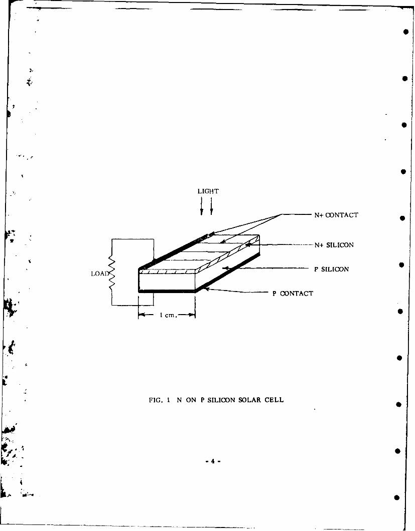
LIGHT
N+ CONTACT
------N+SILICON
FIG. I N ON P SILICON SOLAR CELL
-4-
S
smaller fraction of their power from the red end of the solar spectrum and are there- S
fore less sensitive to degradation of the diffusion length in the base.
C. Solar Cell Performance
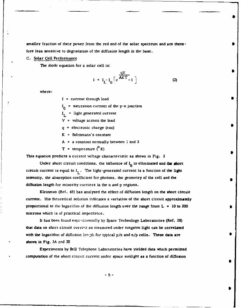
The diode equation for a solar cell is:
qV 5
I iL o AKTl (2)
where:
I = current through load S
10 = saturation current of the p-n junction
I = light generated current
V = voltage across the load
q = electronic charge (esu)
K = 3oltzmann's constant
A = a constant normally between 1 and 3
T = temperature e K)
Thibs equation predicts a current voltage characteristic as shown in Fig. 2
Under short circuit conditions, the influence of I0 is eliminated and the abort
circuit current is equal to I . The light-generated current is a function of the light
intensity, the absorption coefficient for photons, the geometry of the cell and the
diffusion length for minority carriers in the n and p regions.
Kleinman (Ref. 48) has analyzed the effect of diffusion length on the short circuit
current. His theoretical solution indicates a variation of the short circuit approximately
proportional to the logarithm of the diffusion length over the range from L a 10 to 200 0
microns which is of practical importance.
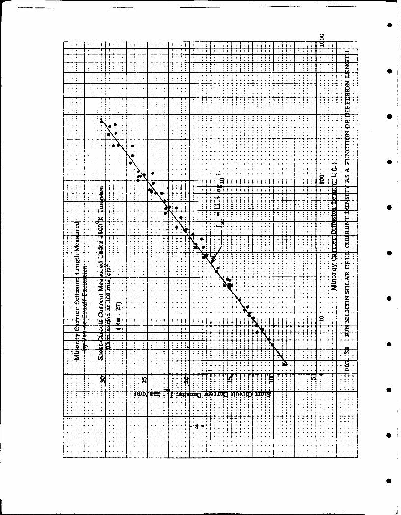
It has been found ex-c,inentally by Space Technology Laboratories (Ref. 28)
that data on short circuit current as measured under tungsten light can be correlated
with the logarithm of diffusion len ,th for typical p/n and n/p cells. These data are
shown in Fig. 3A and 3B
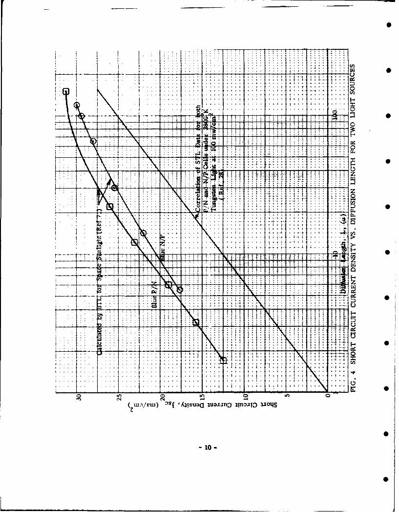
Experiments by Bell Telephone Laboratories have yielded data which permitted
computation of the short circuit current under space sunlight as a function of diffusion
5 -"
-5 - ... . . . .

0
70 F~ ~
1. . .... ...
60 ~ ---
... .... ..
40 . .
.. ~ .... ... ... .... . . .. ..
... .... ...:30 - *
*~~. -4-....... .
. .. .. .. ...
20 . . . . . . ..
. .. : .1 ... ..-~ ~ . ... ... ..- 4 4*4--
20 .- - ... .... -
11- -4-
0 ... ..
.G 20 G. .... ...... 17 z: : ~-
FI.2TYPICAL CURRENT - VOLTAGE CHARACTERISTIC FOR A SOLAR CELL
-6-

.* . . ... . . . . . . . .
0 .* .. . . . . .:a
d.ii-.. ... .. i
... ...... . .j . . . .
t ~ ~ ~ 9 t~t ~ ~
4 T-
i0
. . . . .... .
...... ..........
VAA
. . . . . . . . . . .
. .. . . .. .1 ;. .
..........:. ...*..L... .J ....... -.. -............
tit

length, which are shown in Fig. 4 for comparison with the STL correlation line. It
is noted that there is some departure from linearity with log L for the BTL data on
blue-shifted p/n and n/p cells.
A very significant factor to be noted in Fig. 4 is that the short circuit current 0
does not decrease as rapidly with diffusion length reduction under space sunlight as
when the measurement is made under tungsten light, which is excessively rich in red
light.
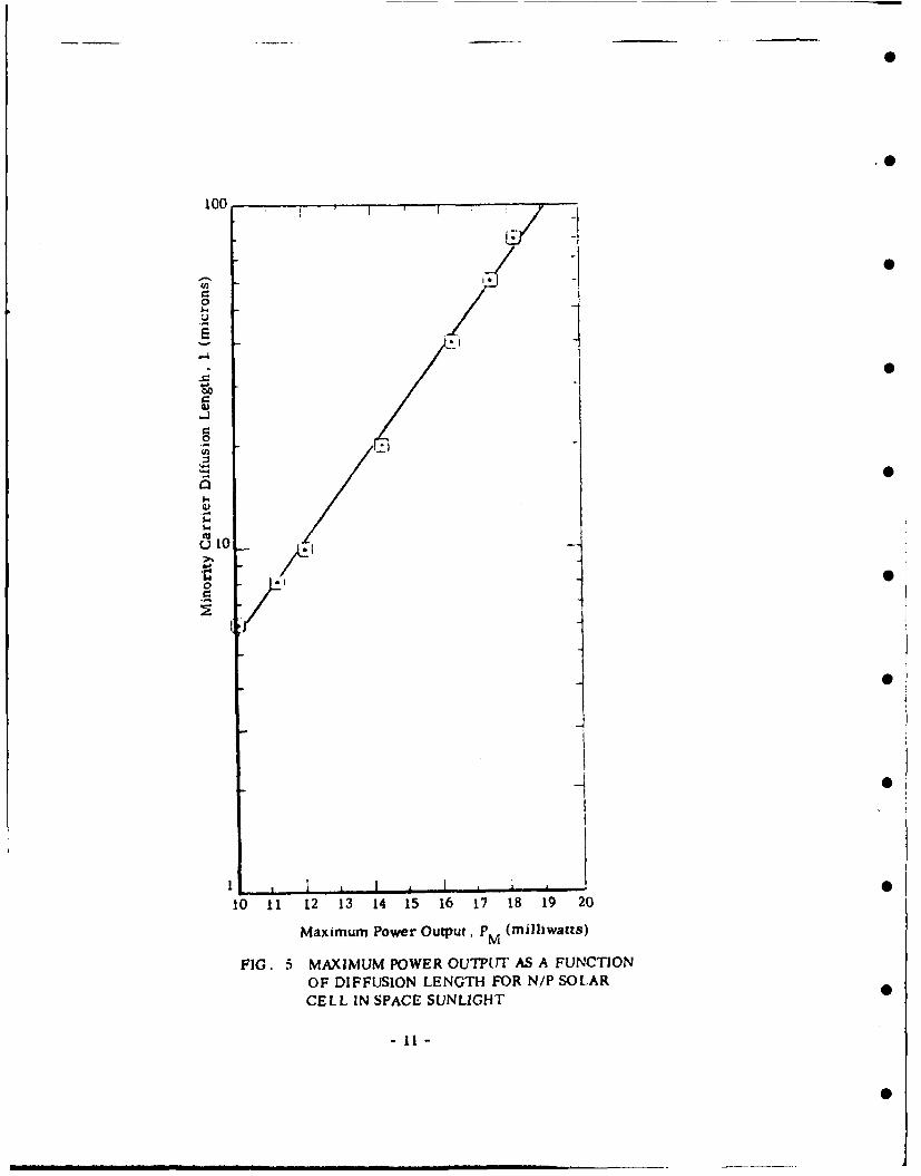
Madey (Ref. 53) has used BTL data (Ref. 75) to correlate maximum power under 0
space sunlight with the logarithm of diffusion length, as shown in Fig. 5.
Based on the empirical evidence, it is assumed that the prediction of solar cell
performance in a radiation environment can be reduced to a calculation of the degradation
of diffusion length, coupled with reference to data which show how the performance 0
parameters of the particular type of cell in space sunlight will vary with diffusion length.
The use of minority carrier diffusion length (or lifetime) to correlate radiation
damage effects is recommended because it is an accurately measurable quantity (see0
next section) which is sensitive to damage by penetrating radiation and is independent
of other solar cell parameters like surface optical reflectivity, surface recombination
velocity, and junction depth, all of which influence measurements of current and
power. •
In nearly all space applications a glass, silica or sapphire cover slide is used
over the cell to aid in radiative heat rejection and to carry a spectrally selective filter
as well as to provide radiation shielding and protection in ground handling. Since the
efficiency of a solar cell varies (logarithmically) with light intensity, it is desirable to 0
use a cover slide material and adhesive (if necessary) which do not darken unde:" space
radiation, or to estimate the decrease in transmittance expected in the wavelength range
of interest (from 0.35 to 1 .1 microns). Pertinent test data are given in Appendix A.
0
-9-
A
.1.41. . . . . ... . . 1 : : "
. .-
*~ .... .... ..I..
H , ., .:-- I
. . . . . 1 14'
. .. .. . .. ... *t
__ + T7 4 t
'z' "eri
+., ,+
. . . .,. . .. .
NC"4 -4
-100
0 .. 0
10 11 12 13 1 5 1 7 1 9 2
FG 30
-. ,
.,
.2.I-I
OF DIFFUSION LENGTH FOR NIP SOLAR
CELL IN SPACE SUNLIGHT
1-II
U 10

III RADIATION DAMAGE TO SOLAR CELLS .
This section includes a discussion of the physics of radiation damage, the
effect of radiation on minority carrier diffusion length, analysis of the degradation
of diffusion length in space using laboratory data on damage coefficients, and shows 0
how the solar cell parameters such as short circuit current, maximum power and
current at a fixed voltage can be correlated with the diffusion length.
A. Production of Defects and Recombination Centers by Radiation
When electrons at energies greater than 145 Key and protons at energies
greater than 98 ev bombard a silicon crystal, they can displace an atom from the
crystal lattice, producing a lattice vacancy and a recoil atom which comes to rest
as an interstitial atom. With high energy electrons or protons, the recoil atom may
have enough energy to displace other atoms before coming to rest. The displacement
of a single atom is called a Frenkel defect. The displacement of two adjacent atoms
is called a divacancy. When very high energy protons ( 500 Mev) interact with a
nucleus they can cause spallation (star production) which results in several nuclear
fragments which stop at short range in the crystal, displacing many atoms.
The crystal defects produced may not be thermally stable except at very low
temperatures. At room temperature the vacancies as well as crystal impurity atoms
can migrate and form stable defects, some of which act as recombination centers for
electrons and holes. The recombination process occurs as the defect center first
captures a minority carrier and subsequently captures a majority carrier, thereby
annihilating an electron-hole pair. The silicon A-center is a stable defect consisting of
a substitutional oxygen atom occupying a site in the silicon lattice. The A-center con-
centration is dominant in determining the diffusion length of minority carriers (electrons)
in p-type silicon when it is irradiated by low energy electrons. P-type silicon is the base
material in radiation resistant n/p solar cells and less susceptible to the formation
of recombination centers than n-type silicon.
The silicon E-center appears to be a vacancy next to a substitutional phosphorus
atom and is produced predominantly in floating zone n-type silicon. Research is
- 12 -
I 0

continuing to understand the nature of other types of defect centers in semiconductors
and to determine whether it is possible to intentionally dope the material in such a
way that the stable defects do not act as recombination centers which decrease the
diffusion length and lifetime (Ref. 79).
The effectiveness of recombination centers in shortening the diffusion length
in silicon is generally not directly proportional to the number of atoms which are
displaced by radiation, but depends on the types of defects that are introduced by
protons and electrons of different energies, which affect the types and concentrations
of the recombination centers that arc formed by interaction with impurities (Wysocki,
Ref. 88, has shown that a simpler situation prevails in gallium arsenide, where the
damage produced by radiation appears to be proportional to the number of atoms
displaced.)
The rather wide scatter in the susceptibility of various types ol pin cells to
radiation damage is believed to be caused by inadequate control of impurities in the
n-type base material which affect the formation of recombination centers.
One effective way to improve the collection efficiency in spite of the presence of
recombination centers is to use a "drift-field" solar cell in which the doping is graded
to spread out the electrostatic field region at the junction. By this technique (Ref. 20),
minority carriers from a larger volume o the :ell arc electrostatically swept to the
junction and are less susceptible to capture by the recombination centers that are 0
present.
B. Simplifying Assumptions
An assumption which is ot great value in simplifying the analysis of solar
cells is that all the pert, rmancc parameters of a particular design of solar cell are 0
unique functiom,, ot the minor.ty carrier diffusion length in the base region. This is
cquivalent to the assumption that the only effec-t of pcnetrating radiation on a solar cell
is to reduce the minority carrier diffusion length in the base region.
This basic assumption is found to be valid when the change in diffusion length
is produced by penetrating particles which generate a fai rly uniform concentration of
de.fects throughout the front 100 to 200 micron thick layer of a solar cell. In general,
protons above ia few Mev in energy and elctrons dlbve 'I few hundred Key in energy
- 13 -
impinging on bare solar cells approximately meet this requirement. However, low
energy protons which only penetrate a few microns or less will primarily damage the
front layer and junction region and the assumption above will be invalid. This more
complicated situation is not treated further here because it is not believed to be of
great importance when cover shields are used. However, it is pertinent in understanding
the behavior of bare solar cells when subjected to low energy protons in space.
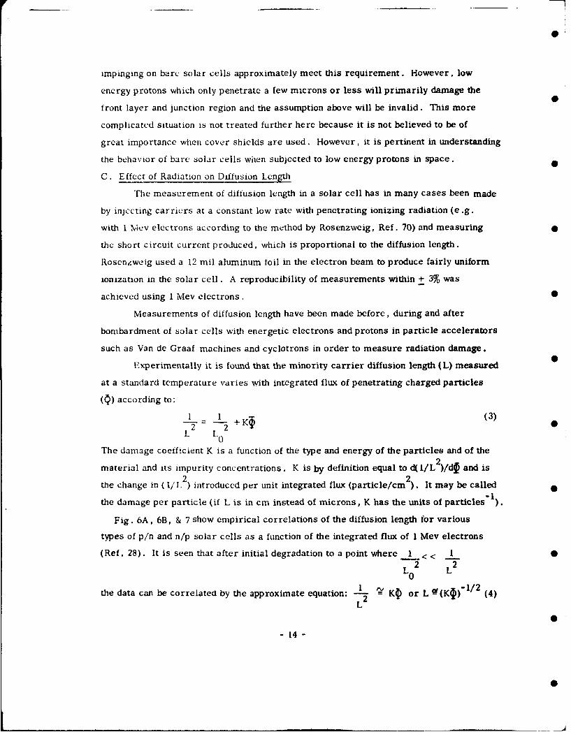
C. Effect of Radiation on Diffusion Length
The measurement of diffusion length in a solar cell has in many cases been made
by injecting carriers at a constant low rate with penetrating ionizing radiation (e.g.
with I Mcv electrons according to the method by Rosenzweig, Ref. 70) and measuring
the short circuit current produced, which is proportional to the diffusion length.
Rosenzweig used a 12 mil aluminum foil in the electron beam to produce fairly uniform
ionization in the solar cell. A reproducibility of measurements within + 3% was
achieved using I Mev electrons.
Measurements of diffusion length have been made before, during and after
bombardment of solar cells with energetic electrons and protons in particle accelerators
such as Van de Graaf machines and cyclotrons in order to measure radiation damage.
Experimentally it is found that the minority carrier diffusion length (L) measured
at a standard temperature varies with integrated flux of penetrating charged particles
({ ) according to:
1 2 +K (3)
L L0
The damage coefficient K is a function of the type and energy of the particles and of the
material and its impurity concentrations. K is by definition equal to d( I/L 2)/d and is
the change in ( 1/ .2 ) introduced per unit integrated flux (particle/cm 2). It may be called
the damage per particle (if L is in cm instead of microns, K has the units of particles ).
Fig. 6A, 6B, & 7 show empirical correlations of the diffusion length for various
types of p/n and n/p solar cells as a function of the integrated flux of 1 Mev electrons
(Ref. 28). It is seen that after initial degradation to a point where I C< 1 02 L2L0
the data can be correlated by the approximate equation: L2 K) or L I(K )"' 2 (4)
L2
-14 -

10 f f f it, P~. JA44+,q f 4f4 i -i;I ;j~f+ -4--Fj -4- +S
+ H f i r4
;,t44404.4 -
-f + i H44 - 4 S
2 ; 0- 12. -
Integrated~~~~- Flxo4 FVEetos Ec
FIG.~~~~~t' -ADFUIN E hDGADTO FN7 OA ELWIT ... .... LCTON
qiS
+Is
10S

--f t~j if, HltH 1 1 ~i -41 + 4. 0
;241 t I
-4.X
LLyo_Tp
4 ., . .. . .- j 4
sm 42Ine+ae Flu of 7 ME Electrons ll(E/1,;
FI. B IFUiO LN~hDERAAIO4O=PNSOARCELWI~hI ME ELETRON
-N 1,t!
100
t.i W : i-o. . - ..:M7: : "71- T , ::0
44 :::7 S 4 .
4 -40
tj0
AN. + .. ...
-4 1!7
Ff I 3 H l t ; 1
In Fig. 6A it is seen that the data for n/p cells from three manufacturers
using I ohm-cm p-type silicon for the base material all cluster quite closely together. 0
The improved radiation resistance of cells with higher base resistivity (higher purity)
is also clear, with one possible exception.
In Fig. 68 It is noted that p/n cells exhibit a large scatter in the data, preunably
because of variations of the impurity content in the base material. (However, Weller 0
(Ref. 83) has shown that oxygen content does not control the recombination of minority
carriers in p/n cells when irradiated with 4.8 Mev protons).
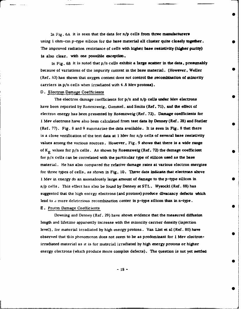
D. Electron Damage Coefficients
The electron damage coefficients for p/n and n/p cells under Mev electrons 0
have been reported by Rosenzweig, Gummel, and Smits (Ref. 71), and the effect of
electron energy has been presented by Rosenzweig (Ref. 72). Damage coefficients for
I Mev electrons have also been calculated from test data by Denney (Ref. 28) and Statler
(Ref. 77). Fig. 8 and 9 summarize the data available. It is seen in Fig. 8 that there
is a close verification of the test data at I Mev for n/p cells of several base resistivity
values among the various sources. However, Fig. 9 shows that there is a wide range
of KE values for p/n cells. As shown by Rosenzweig (Ref. 72) the damage coefficient •
for p/n cells can be correlated with the particular type of silicon used as the base
material. He has also compared the relative damage rates at various electron energies
for three types of cells, as shown in Fig. 10. These data indicate that electrons above
I Mev in energy do an anomalously large amount of damage to the p-type silicon in 0
n/p cells. This effect has also be found by Denney at STL. Wysocki (Ref. 88) has
suggested that the high energy electrons (and protons) produce divacancy defects which
lead to a more deleterious recombination center in p-type silicon than in n-type.
E. Proton Damage Coefficients •
Downing and Denney (Ref. 29) have shown evidence that the measured diffusion
length and lifetime apparently increase with the minority carrier density (injection
level), for material irradiated by high energy protons. Van Lint et al (Ref. 80) have
observed that this phenomenon does not seem to be as predominant for I Mev electron-
irradiated material as it is for material irradiated by high energy protons or higher
energy electrons (which produce more complex defects). The question is not yet settled
-8-

I . !
. .. . . .. . . . . . .
. . .. . . . . .I
010
t .s~ V?
.. ... .. .
E.etro Energ .. E..
PIG.O ~ ~ ~ ~ ~~. ELCTO DAAG ..FFCIN ... A .. ..CINOFEETON E
10-~~ ~ ~ ~ 10, .-
4 +

0
[ 5 1- - ------------
. . .. . . . . . . .
.:V :. ... .. .0.
. ...... V ... .... . . . .. .. ... . .0K.. ..
LIE - I I I-H-+- t++0
OF0

LQI
... ~ .. . . .. .
I
. . . . . . . . . . .
. . . . .. . . .
.0 .. . . . . .- . ..-- . .- .. - .
0ice
0. '72~ LIM ~ 1 2! !!,
+44
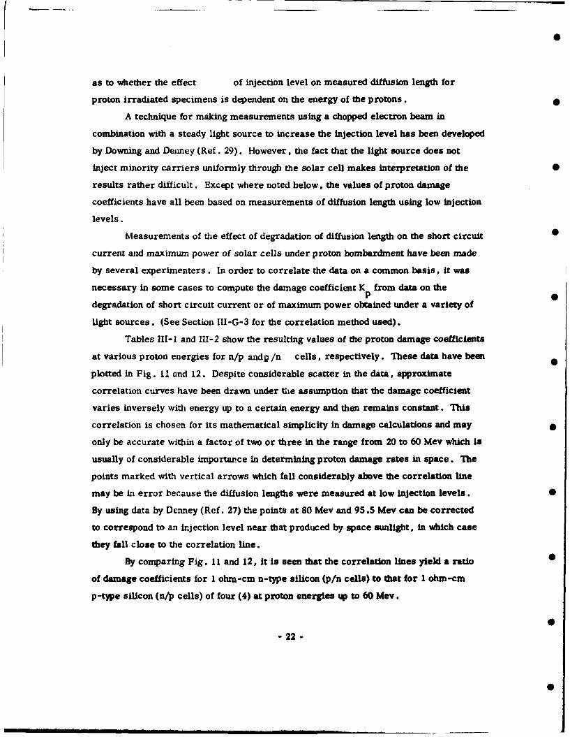
as to whether the effect of injection level on measured diffusion length for
proton irradiated specimens is dependent on the energy of the protons.
A technique for making measurements using a chopped electron beam in
combination with a steady light source to increase the injection level has been developed
by Downing and Denney (Ref. 29). However, the fact that the light source does not
inject minority carriers uniformly through the solar cell makes interpretation of the 0
results rather difficult. Except where noted below, the values of proton damage
coefficients have all been based on measurements of diffusion length using low injection
levels.
Measurements of the effect of degradation of diffusion length on the short circuit 0
current and maximum power of solar cells under proton bombardment have been made
by several experimenters. In order to correlate the data on a common basis, it was
necessary in some cases to compute the damage coefficient K from data on theP Sdegradation of short circuit current or of maximum power obtained under a variety of
light sources. (See Section III-G-3 for the correlation method used).
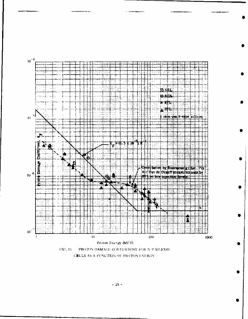
Tables l1-I and 111-2 show the resulting values of the proton damage coefficients
at various proton energies for n/p and p/n cells, respectively. These data have been
plotted in Fig. 11 and 12. Despite considerable scatter in the data, approximate
correlation curves have been drawn under the assumption that the damage coefficient
varies inversely with energy up to a certain energy and then remains constant. This
correlation is chosen for its mathematical simplicity in damage calculations and may •
only be accurate within a factor of two or three in the range from 20 to 60 Mev which is
usually of considerable importance in determining proton damage rates in space. The
points marked with vertical arrows which fall considerably above the correlation line
may be in error because the diffusion lengths were measured at low injection levels. 0
By using data by Dcnney (Ref. 27) the points at 80 Mev and 95.5 Mev can be corrected
to correspond to an injection level near that produced by space sunlight, in which case
they fall close to the correlation line.
By comparing Fig. I and 12, it is seen that the correlation lines yield a ratio 0
of damage coefficients for I ohm-cm n-type silicon (p/n cells) to that for I ohm-cm
p-type silicon (n/p cells) of four (4) at proton energies up to 60 Mev.
0- 22 -
0
TABLE 111-1
Proton Damage Coefficients for 10 -cm p-Type Silicon (n/p Cells)
Proton Energy MEV Damage Coefficient, Kr Reference
1 .8 3.2 x 10- 6 6
4.8 1.7 x 10 6 83
8.3 2.1 x 10- 6 7* S
16.8 8.3 x 10- 7 70- 6
17.6 1.0 x 10 6- 7
10.0 9.2x 10 7*-7
20.5 4.0 x 1O 23*
45.0 1.0x 10 6 57
80.0 6.0 x 10 7 57
95.5 2.4 x 10"7 23
95.5 5.4x I0 23
120 4.0 x 10 7 57
130 3.3 x 10- 7 70
450 1.8 x 10 7 23-7750 2.8 x 10 23
* K was calculated from the authors' values of LO L and Q.
** The 0 's from six types of cells were averaged and converted to a K value.
I
- 23 -

TABLE 111-2
Proton Damage Coefficients for 1.Q -cm n-Type Silicon (p/n Cells)
Proton Energy, ME V Damage Coefficient, K ReferencePS
1.8 1.0 x 10.5 6
4.8 8.7x 10- 6 83
8.1 1.2 x 10"5 7"
16.8 5.1 x 10 "6 7017.6 5.9 x 10" 6 6
20.5 7.9x 10 23
45.0 6.0 x 10- 6 57
80.0 4.0 x 10"6 57 S
95.5 3.0x 10 23
95.5 2.26 x 10⁻⁶ 23
130 2.0 x 10⁻⁶ 70
450 3.I x 10"7 23
450 1.2 x 10.6 57
740 4.2 x 10 23
I
K p was calculated fron the ,lthors' values of L0 , L and 0.
- 24 -
i d P
0- 4
F-- *t--* r -r4--
I iT:
.. ... ...
'p- _. 77ALL2PEI: i :::t1!
10 1 t ...
PrtnI-nty MV
FIG I I Rl)\DMCECFF .IN ORNPSllN)
CELL AS i~rL,,riN+ m II()IYN E ERM
25

1 1.j: 1 1 0
10
N A. *b2 4+-- 14~
-- 2t 4-4
-AS

The damage coefficients at proton energies of 1 Mev and lower are only of
interest for bare solar cells, which degrade very rapidly when exposed to geomagnetically-
trapped protons.
The proton damage coefficients as a function of proton energy E may be approxi-
mated by the following relations: 0
For 1 ohm-cm p-type silicon (n/p cells):
Kp = l.SX 10-5E I for I < E ' 60Mev
Kp = 2.5x 10 for E > 60Mev
For 1 ohm-cm n-type silicon (p/n cells): S
Kp =6x I - 5 E-I for I< E : 150 Mev
Kp =4x10 for E > 150Mev
F. Calculation of the Diffusion Length From Laboratory Data
If more than one type or energy of bombarding particleE i-s present, it is a
good approximation to assume that the damage (the differential change in I/L 2) is
additive and independent of the rite of irradiaticn. It is also uLually assumed that the
damage is independent of tto t, inperature and the operatng coidition of the solar cell
during irradiation, although it is known that radiation effects can anneal out at elevated
temperature.
inder these assulnptiois, when scveral typc: of partic'es are present
simultaneously or in sequence,:
'L f> ' I 22
If the r.!Aiation in , h' .'i a continous energy spectrum, it is convenient to
define a damna-% itegr, i 'i., . c, : n:
U I- 0
where .(E ,t) omnirdilLctor.'l ilu% p. r ui i; energy interval in space S
(particles/cm _sec-Mev) ,Lt tklmu t ,yt !r.ohhdf by CiLc ,lud over the solar cell.
K(E) = damage coeficient at rergy L.
- 27-
S!
The factor of 1/2 is introduced to account for the usual assumption that there
is infinite shielding on the back side of the solar cell.
A laboratory irradiation to a time integrated flux 01 with particles of energy
E is equivalent to a space irradiation if1t
KIQ 1 = 2. (E,t) K(E)dEdt (7)
where K is the damage coefficient for particles of energy E l .
If E I is taken as I Mev electrons, Equation 7 defines the 1 Mev unidirectional
normal incident integrated flux )1 which is equivalent to a certain irradiation for a
time t in space.
For shielded solar cells, the spectral flux p(E ,t) and the corresponding damage
coefficient K should be based on the flux and energy spectrum present behind the shield
at the surface of the cell, if the damage coefficient K has been measured for bare cells.
Also it is assumed that the particles penetrating the shield have a range longer than about
200 microns and produce uniform damage in the sensitive base region of the solar cell.
The equivalence between doses (integrated fluxes) of particles at any arbitrary
energy E and the dose at energy E can be established by the relation:
Kn K n = K2 ]n L L (8)
K 0or: : (9)
The ratio (K nK ) is the relative damage rate for particles of energy En as
compared to energy E
G. Correlation of ,h-- Performance of Solar Cells as a Function of Diffusion Length
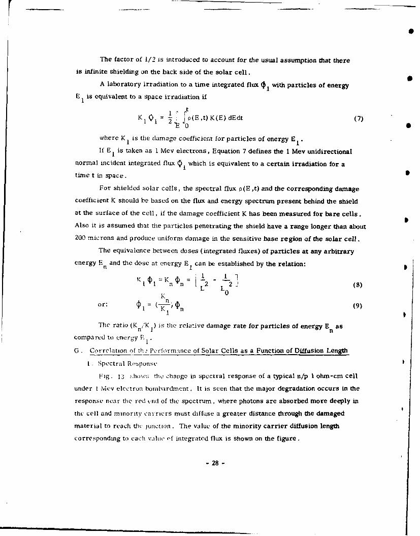
1. Spectral Response
Fig. 13 ,,how 3 the change in spectral response of a typical n/p 1 ohm-cm cell
under I viev electron bombardment. It is seen that the major degradation occurs in the
response near the red tund of the spectrum, where photons are absorbed more deeply in
the cell and minority carriers must diffuse a greater distance through the damaged
material to reach thc junction. The value of the minority carrier diffusion length
corresponding to each value rf integrated flux is shown on the figure.
- 28 -

0.7
. . .~ . . . . . . .
.... ... ........................... .... ...........
0. .: . .,1~'S
. . . ... .. .. ..
. . . . . . . .
0.3 .....

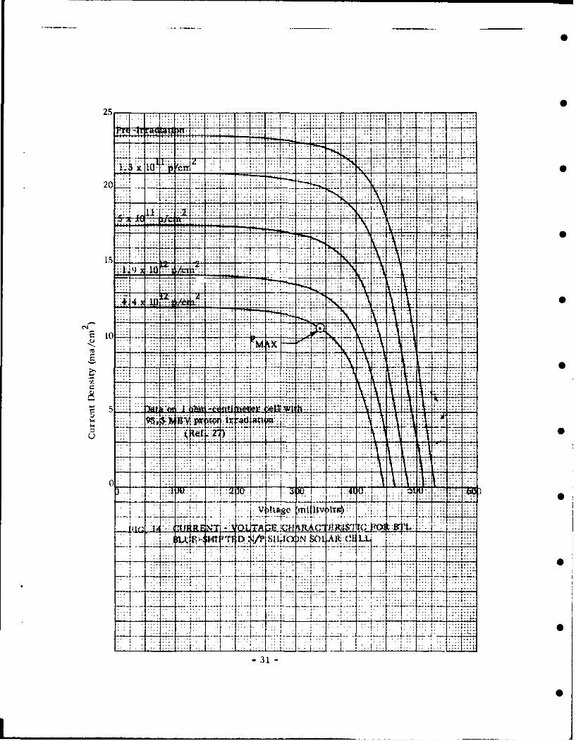
2. Current - Voltage Characteristic
Fig. 14 is a typical plot showing the change in the current-voltage (i-V) character- 0
istics of a solar cell after various degrees of irradiation. It is seen that the short
circuit current degrades more rapidly than the open circuit voltage
3. Short Circuit Current
It was shown in Fig. 3A, 3B, and 4 that the short circuit current and maximum 5
power of solar cells can be correlated with the diffusion length. However, the particular
correlation obtained depends on the spectral distribution and intensity of the light source
used, and the presence or absence of an anti-reflection coating on the cell (which0
typically increases the power output by at least 25%, Ref. 75). Also, the initial value
of short circuit current or power obtained from a particular cell will be a function of
the initial diffusion length of the particular piece of silicon from which it was made,
as well as of differences in surface recombination properties and other properties due
to manufacturing tolerances.
If one assumes reasonably close control of the manufacturing process, then
it should be possible to select an average value for the initial diffusion length and
corresponding average values of the initial short circuit current and maximum power •
as measured under a particular light source which are representative of the particular
type of production cells. It is then desirable to predict what the cell performance will
initially be in space sunlight and how the performance parameters will degrade as the
diffusion length is reduced by radiation. 0
In order to obtain a generally applicable procedure for predicting performance,
the following method was used:
If we assume that short circuit current (I) for a particular type of solar cell
varies directly with the logarithm of the diffusion length (L), then one can write: 0
1 =C In( L (6)L
where C and L' are constants which depend only on the light source.
Then the short circuit current ratio is:
I = In (L/L ) (7)
0 In (Lo/L)
- 30 -
25 ... ... ... ......... .....
20.. . .... ..
+" .. _. . ... ..
-77-
15~ I.. ... ...
x J : - ' : .......v... .. .........H .
4 F7 .... ... _N Al LL wIo .. 1 .....
.1 ..... ...
- 31 V
5 ... ..

which can also be written as:
IL -10=o I + In' I1 L L (0
This equation indicates that for a given light source, which determines L,
and with a given initial diffusion length L0 , the term In (L0 /L" ) is a constant and the
short circuit current should degrade linearly with the term In (L/Lo).
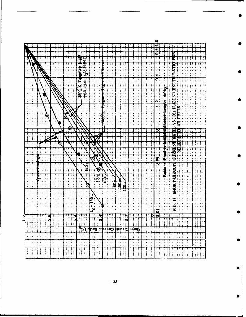
Fig. 15 shows the variation of short circuit current ratio with the logarithm
of the ratio of final to initial diffusion length for three different light sources. The
curves shown are based on measurements for both p/n and n/p cells by Rosenzweig, 0
Gummel and Smits (Ref. 71), Denney, Downing and Van Atta (Ref. 28) and Weller
(Ref. 83).
Data from Weller (Ref. 83) for measurements with water-filtered tungsten
light show that Equation 8 is approximately satisfied. Data computed for space sunlight S
(Ref. 71) appear to depart somewhat from linearity as may be seen in Fig. 15 •
However, the use of the dimensionless parameter (L/L 0 ) to correlate test
data is still useful as a technique for predicting short circuit current ratio. Using
the curves in Fig. 15 it is only necessary to know L0 to predict the degradation of
short circuit current ratio with L. It is believed that the curves in Fig. lSwill permit
estimating the short circuit current ratio for blue-shifted silicon solar cells correspond-
ing to any value of L from 10 to 200 microns with reasonable accuracy, independent
of whether the cell is n/p or p/n, with base resistivity values from I to 10 ohm-cm,
and with initial diffusion lengths from 100 to 200 microns.
The problem of prcdicting the absolute value of initial short circuit current
under space sunlight from ground measurements with other light sources is not con-
sidered here. (See Ref. 71)
By cross-plotting from Fig. 15, the value of the diffusion length required to
yield a 25% reduction in short circuit current under various light sources is plotted
as a function of the initial diffusion length in Fig. 16. 0
From the value of L determined from Fig. 16, the change in (I/L 2) required to
produce 25o degradation in short circuit current under various light sources can be
- 32 -
I. T 1i .
4--4
4 1 i i -
~r.
b4--.
. . . . . . . .. . . ..
. . . . . . . . . . ..
.:77
33 -

.. ... ... .....F7 . ........
... ... .... ...
..... .......- - - - - -
II - - - - - -
t4!!. .. .. ..
..1. .. ... .... .....
- = .. ...-..
..~N . ~ ... ... . ....I -'0 ~ ~ ~ 1 ... .. I~ .. ... .. ...... ... .... .... ... .. ... .. .
...... ... ........ .. . .
77' .I..EA. .I....... .. . .. . . o t i, p ... ...
34.
... .. . ... 1S

computed. This value is calculated to be 4.1 x 105 cm "2 based on data for blue n/p
cells with L0 = 120ti in space sunlight.
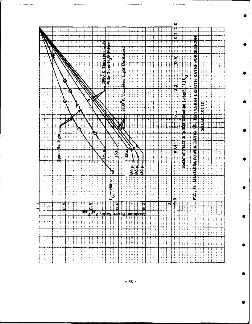
4. Maximum Power Output
A typical plot of the variation in the maximum power ratio as a function of the
short circuit current ratio is shown in Fig. 17. It is seen that the maximum power
decreases only slightly more rapidly than the short circuit current.
Fig. 18 shows the power output of n/p solar cells as a function of cell voltage
at various degrees of degradation produced by I Mev electrons. These data for space
sunlight have been correlated in dimensionless form as maximum power ratio vs. 0
diffusion length ratio in Fig. 19, along with the comparable data for filtered and un-
filtered 28000 K tungsten light. Data computed for space sunlight (Ref. 71) for blue
p/n cells with an initial diffusion length of 150 4 are included.I
5. Power at a Fixed Voltage
The rate of degradation in solar cell current when operated at a fixed cell voltage
(as when connected to charge a battery) depends on the value of the operating voltage.
If the operating voltage is chosen too high, the cell current will degrade very rapidly.
On the other hand, if the cell voltage is too low, then the maximum power available
may not be obtained. It is seen from Fig. 18 that if the cell is to operate until its
diffusion length is degraded to about 7.6 microns, the cell voltage should be selected
at approximately 0.40 volts in order to obtain maximum available power at the end of
life. However, consideration of temperature coefficients may force selection of a
lower voltage.
6. Temperature Coefficients of Solar Cells as a Function of Radiation Damage
Martin, Teener and Ralph (Ref. 55) have investigated the temperature coefficient
of silicon solar cells using a Spectrosun solar simulator. They found that the temperature
coefficient of short circuit current for n/p 10 ohm-cm cells increased from an initial
value of about 60 i amp/°C to 102.5 jamp/ C after irradiation with a flux of 10 i Mev,2 o
electrons/cm . The value for p/n I ohm-cm cells increased from 62.5 to 100 j A/°C.
However. the temperature coefficient of open circuit voltage stayed constant at about
-2.24 mv/ 0 C for the n/p cells and -2.05 mv/ C for the p/n cells. Ross (Ref. 73)
measured a temperature coefficient for the maximum power voltage of about -2.08 mV/ C
for both n/p and p/n cells.
- 35 -

. ~~ . ... ,...
-44-
.... ....... .. . . .44 -I
-4
-4
:242~-L -1 +-I.0 .
*~~~~ T 4j4
* i~±i#.ji~+
-4- 4-
-36-I
0.4 t

.. ... .
20.
14
12 ~ ~ ~ - r T IT 1
-2
0 ~ ~ .. .. . 2t j ...
... .. .... ... : i L ~
- - -~~~~~.. F - .'--- * ~ - ...... ..-
J: 7
* .. . . 4. . :
. .. .. . . ...
94~
*V N
. . . . . . ...
. . . . . . . ... ...
icS
-4r
38j

it is important to recognize that the temperature coefficient of short circuit
current would be about a factor of ten too high if measured with a tungsten light
source, which overemphasizes the red response as compared to sunlight and therefore
overstresses the effect of variation of minority carrier lifetime with temperature.
Unless the negative temperature coefficient of open circuit voltage is taken into
account, the operating voltage point may be selected too close to the open circuit
voltage and very severe degradation of performance will occur as radiation damage
proceeds.
Experimental results on the combined effects of temperature and radiation
damage on the I-V characteristics of solar cells as reported by Martin, Teener and
Ralph (Ref. 55) are shown in Fig. 20,21, 22, and 23. By reference to these figures, 5
the operating voltage point may be selected so that maximum power is obtained after
degradation to the required value of equivalent I Mev electron flux (or corresponding
diffusion length).
0
3
I
I
, ik m o• -

70 Q 0
10 0C (From Martin, reener, &Ralph, Ref. 55)
600
20 ~ ~ ~ 1 0______ ______
0~~~7 0_____ C____
Voltage - -- (Volts)
FIG. 20 CUTRRENT VS. VOLTAGE CURVES FOR N/P 10 OHM-CMSILICON SOLAR CELLS AT VARIOUS CELL TEMPERATUJRESBEFORE AND AFTER I MEV ELECTRON IRRADIATION
-40 -

70 __ _ _ _ ~ 0$10~ e/cm2
_ _
200
1 0 __0__
30.1..34.5.
Votge)(Vls
20 G 21 CU R N S O LT G U V S F R P N 1 O M C
1 .2 .3 41 .
Voltae - (olts

N/P 10 OHM-CM SOLAR CELLS1 vs. T
Vvs. T-P OC vs..T
max
700 Data from average of 10 cells .=101 e/cm2
60 ___ ____.6
S50 ___ .5
0
__ _ _ 115 >___
4 0 10___ .4
20 40 60 3000CELTMEAUR E.C
10 ~ ~ 42 .2 2
5 x 1' 91

P/N I OHM-CM SOLAR CELLSI vs. T
V ocvs. T- - -
OC vs. T - -
maxData from average of 10 aells
70 .7
00
60 Z: ,,.6
50 __ __ _ .50
5 1 1
0S
3 0. -
1 02 4 1 w.2
0.-- .2 10
10 100
CELL TEMPERATURE ( DEG. C )
FIG. 23 ELECTRICAL CHARACTERISTICS AS FUNCTIONS OFTEMPERATURE AT INCREASING LEVELS OF I MEVE LE CTRON F LUX FOR P /N SO LAR C E LLS,
-43 -

IV THE SPACE RADIATION ENVIRONMENT
(See also recent Reference 145 in the July 1963 issue of the Bell System Technical Journal)
A. Introduction •
The most damaging space radiations for solar cells are the geomagnetically
trapped electrons and protons in the magnetosphere and the solar flare protons which
occur sporadically at times near maximum solar activity and which are observed
primarily outside the magnetosphere. Other radiations which are generally negligible •
with respect to radiation damage on semiconductors include primary galactic cosmic
rays (which are primarily protons and heavier ions), neutrons produced by cosmic ray
interaction with the atmosphere, solar x-rays and gamma rays.
For earth satellites within the magnetosphere, it is important to know the flux and
energy spectra of electrons and protons encountered in order to calculate radiation
effects. An excellent survey article as of October 1962 was prepared by O'Brien
(Ref. 104). Unfortunately, recent experimental data on trapped electrons and protons
has not yet been properly correlated to provide a good knowledge of the flux and energy
spectrum of trapped particles at all locations. Furthermore the "Starfish" nuclear
explosion of July 9, 1962 injected large numbers of artificial electrons which are still
decaying so that the electron fluxes are still changing with time. Therefore, the brief 0
summary below must be considered tentative and subject to change after further
correlation of experimental measurements.
B. Mc llwaln's Coordinates
In order to discuss the distribution of trapped particles it is most convenient to 0
use the coordinate system developed by Mc Ilwaln (Ref. 99). The two coordinates are
B, the scalar magnitude cf the magnetic field, and L, a parameter that is very nearly
constant along each magnetic field line and which is nearly equal to the radial distance
to the field line at the geomagnetic equator. Fig. 24 shows an example of L lines plotted •
with respect to magnetic dipole coordinates R and X, taken from (Ref. 99) where R
is the distance from the center of the magnetic dipole and X is the geomagnetic latitude.
"44"

MagneticPole = 0.55 B 0.05 puss•
B 0,011 guss
~~~~L = 3 earth_.-.__.EARTH radi
FIG. 24 THE B- L MAGNETIC COORDINATE SYSTEM
The trapped particles may be visualized as moving primarily in helical paths
around each magnetic field line (. constant L) and being reflected betvm mirror
points north and south of the magnetic equator at points where the field B has increased
over its value at the equator by the ratio (1/sin2 a) %here a ft pitch angle of particle at0 0
magnetic equator. Each particle bounces between the north and south mirror points
with a period of the order of seconds or less. In addition, electrons drift eastward and
protons westward with a period of the order of a minute required to circle the earth,
although this longitudinal motion can be neglected in understmading the steady sate
flux distributions in the belt.
The fluxes and energy spectra of particles can be correlated analytically quit.
well with respect to the B-L coorainate system. The pitch angle distribution of the
particles can also be correlated with the variation in the magnitude of the field B along
each line of constant L. The flux is higher perpendicular to the magnetic field Une than
parallel to the field line, particularly at the mirroring points. This effect of pitch angle
distribution is significant for a satellite (like ANNA- IB) which is oriented with respect
to the magnetic field. However, generally the flux may be defined in terms of an average
omnidirectional flux at a point in B-L space.
- 45 -

An alternate plot of the relationship between the B-L coordinates and the geomagnetic
coordinates R and /. is shown in Fig. 25. In converting from B-L coordinates to earth-
centered coordinates it must be recognized that the earth's magnetic field, if approxi-
mated as a simple dipole, is centered at a point located 411.4 Km from the center of
the earth on a line toward the point at 150.8 degrees east longitude and 15.6 degrees
north latitude (Ref. 3 ). The axis of the dipole is tilted at an angle of 11 .7 degrees
from the earth's axis toward the geographic longitude of 69 degrees west.
Even if fluxes in the B-L coordinates were known precisely, in order to predict
fluxes at an arbitrary point in space with an accuracy better than a factor of 10 it is S
necessary to include the anomalous variations in the magnetic field of the earth from
the dipole approximation. An Important example is the South Atlantic Anomaly, where
magnetic field lines dip to low altitudes and appreciable fluxes of trapped protons and
electrons are encountered at altitudes of only 1000 Km.
C. Electron Fluxes and Energy Spectra
The flux of natural electrons in the inner region of the magnetosphere have been
augmented by artificial electrons injected by high altitudc nuclear explosions. Table IV-l
lists the explosions which have produced measurable effects. Of these, only the
"Starfish" explosion on July 9, 1962 has produced a long-lasting belt of electrons which
is of importance in affecting solar cells.
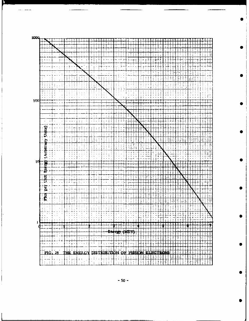
Hess (Ref. 96) has prepared maps of the artificial electron belt in B-L and Ro-,
coordinates (Fig .26 and 21 which are applicable for a time of one week after the
"Starfish" explosion on the assumption that the electrons all have a fission spectrum
as shown in Fig. 28. This map by Hess showed appreciable fluxes of electrons at
values of L up to 4 (altitudes up to 3 earth radii at the magnetic equator). However,
data by Van Allen (Ref. Ill) indicated that the fission electrons were confined to lower
values of L. It now appears that the fission spectrum is approximately applicable only
for L less than 2 and that the electron spectrum is softer (a steeper variation of flux
with energy) than a fission spectrum for L greater than 2, where many of the electrons S
observed were naturally present prior to '"Starfish". An effort is now being devoted by
Hess at the Goddard Space Flight Center to correlate the electron spectra as a function
of L (Ref. 40). Until this correlation becomes available it seems appropriate to assume
- 46 -

Plotted according to the transformation:
B=M (4 R) 1/2 RLcs2
.32
.28 _ _ _ _ _ _
.24__ _ ____ __ _ _ __ _
ci 16 _ __ _ _
c.12_ __ _S
.08 ___ __ _
1.0 1.2 1.4 1.6 1.8 2.0 2.2 2.4 2.6 2.8
L (Earth Radii)
FIG. 25 THE MAPPING OF THE POLAR COORDINATES R and k ONTOTHE B - L PLANE
- 47 -

0.4
Flux, P, in electrons/cm -sec.:3o10/ 10 6 fission energy spectrum is
assumed to apply for L <2
0.3 - -
ax 10
I /3o/6
0.2 , Spectr ' \
0.Uncertain \\
I, I
/Equa\tor(From Hess, Ref. 39)
Equatori [ ... \ I I
01 - I
2 3 4 5 6 0L (Earth Radii)
FIG. 26 THE B - L MAP OF ELECTRON FLUXES APPROXIMATELY ONE WEEKAFTER STARFISH
- 48 -
I I II S

107106
go - - - -
EARTH- -~ 2- E;R
- .40=
(From Hess, Ref. 39)
FIG,. 27 THE R - X MAP OF ELECTRON FLUXES APPROXIMATELY ONE
WEEK AFTER STARFISH
- 49
r : .7 ...
N! I
44- ~ 44-P
1 Ht
0-T Ad S1H 1
T~ T 0 -
I L: A11 i l, 1S
1. .'.
that Hess' map as shown in Fig. 27 applies approximately for values of L less than 2
and that the fission spectrum as shown in Fig. 28 applies in this region. However, it •
is clear that the electron fluxes have continued to decay since one week after Starfish
and that the flux values appropriate at a time of 5-1/2 months after Starfish (Dec. 1962)
may be approximately a factor of two lower than shown in Fig. 27. Until further
correlation work is completed, it does not appear useful to try to calculate electron 5
fluxes and spectra for L values from 2 to 4.
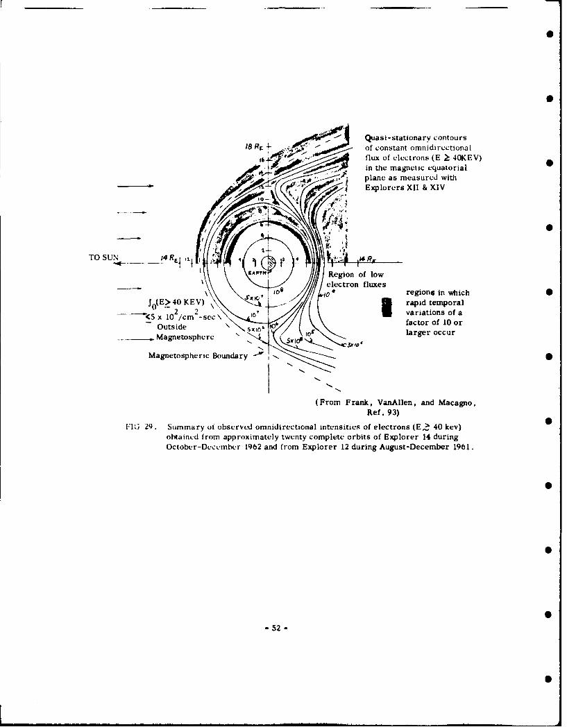
The average electron fluxes in the outer zone (i .e., for values of L greater
than 4) are shown in Fig.29 (Ref. 93). It should be noted that the electron flux in this
region fluctuates radically during each day , Ref. 103) and also as a result of geomagnetic
storms (Ref. 108) and that the applicable energy spectra in this region are not well
established. It is seen in Fig. 29 that the average shape of the constant flux contours In
the magnetic equatorial plane are distorted by interaction with plasma from the sun
(the solar wind).
D. Proton Fluxes and Energy Spectra
Mcllwain and Pizzella (Ref. 100) have shown that the energy spectrum of
protons throughout the magnetosphere may be approximated by the equation:
P (E) d E =(Constant) eE/EO dE (9)
with-5 E =306L "5 . 2 Mev (10)
This equation gives a reasonable fit to the data for values of L up to 8 and is in not
bad agreement with Naugle and Kniffen's spectra (Ref. 102) obtained with an emulsion
experiment at L values from 1 .47 to 1 .79.
The value of the constant which defines the absolute flux at any point may be
approximated by using the proton flux map of Fig .30 (Ref. 101), which shows contours
of the integral flux above 31 Mev. Improved proton maps are being prepared by Walter
L. Brown of Bell Telephone Laboratories and by the Goddard Space Flight Center in
cooperation with the experimenters. •
Additional pertinent references on the space environment are included on page R-7.
It is expected that improved correlations of data on the fluxes and energy spectra of
trapped radiation will become available in the near future, in which case more accurate
calculation of space radiation effects will become feasible. S
- 51 -
Quasi -stationarV contours18 Rr. - of constant omnidirectional
16 ~ flux of electrons (E '4 4OKEV)in the magnetic equatorialplane as measured with
~ ~ Explorers XII & XIV
TO SUN 14 R4R
Region of lowelectron fluxes
XK oregions in whichJ()(E>40 KEV) ~\3 rapid temporal
_ _<5x '1 2 /m 2_secvariations of a
Outside factor of 10 or
Magnetosphere Sf16IE4larger occur
Magnetospheric Boundary - . *-.
(From Frank, VanAllen * and Macagno,Ref. 93)
FIG 29. Summary of observed omnidirectional intensities of electrons (EZ 40 key)obtained from approximately twenty complete orbits of Explorer 14 duringOctober-December 1962 and from Explorer 12 during August-December 1961.
-52-
(Based on Mc Ilwains DataFrom Naugle & Kniffen 0Ref. 102)
660
100 Magnetic Field Lines50,
-- 1000 PRoQroS (E>31 MMV,0 2 CMz SEC -
40 --
30
3 - 34
FIG. 0 PRTNFU A
10-3

TABLE IV-1 S
Data On Nuclear Explosions Which Injected Particles Into The Magnetosphere
Country Identification Size Location Date Remarks
U. S. Teak & Orange I MT Less than 50 mi. above Aug I and Effects disappearedJohnston Island 12, 1958 in a few days due
to particleabsorption in theSouth AtlanticAnomaly.
U. S. Argus (3 shots) 1-2 300 mi. above South 1958 Artificial beltsKT Atlantic lasted several
weeks.
U. S. Starfish 1.4 250 mi. aboveMT Johnston Island 7/9/62 Produced long-
lasting belt ofartificial electrons.
USSR 3 shots ? High altitude and high 10/22/62 Artificial electronlatitude 10/28/62 belts in slot
11/1/62 between inner 5and outer zonesdecayed rapidly.
-54-

V CORRELATION OF SATELLITE TEST DATA ON
SOLAR CELL PERFORMANCE
This section summarizes the results of telemetered performance data for
solar cells with various thicknesses of transparent shielding on satellites which have
been subjected to radiation in the natural and artificial radiation belts.
Table V-I shows the orbital parameters and date of launch of fourteen satellites
for which telemetered solar cell data were available. In most cases, the telemetered 0
data were available in the form of short circuit current with normal solar incidence
angle as a function of time in orbit. Although the temperature of the solar cells was
telemetered in some cases, no effort has been made to correct all data to a standard
temperature.
An example of the variation of short circuit current ratio (I/I) with time for
p/n and n/p silicon solar cells with various shield thicknesses on three satellites is
shown in Fig. 31. The flight test data were extrapolated where necessary to estimate
the time In orbit required for the short circuit current to decrease by 25%. These
extrapolations were made in most cases by assuming a 20% reduction in short circuit
current per decade of time after at least 10% degradation had occurred, except where
test data showeda different trcnd. This extrapolation procedure is inaccurate when
the radiation exposure is not constant with time, which is the case for many satellites
where apogee precession affects the flux encountered per orbit. Table V-2 shows the
data on the extrapolated life to 75% of initial short circuit current for solar cells on
various satellites. The shield thicknesses have been converted to grams per square
centimeter.
The estimated time in days for the n/p solar cells to degrade by 25% have been
plotted against the shield thickness in grams per square centimeter in Fig. 32. A
similar plot of the data for p/n solar cell is shown in Fig. 33.
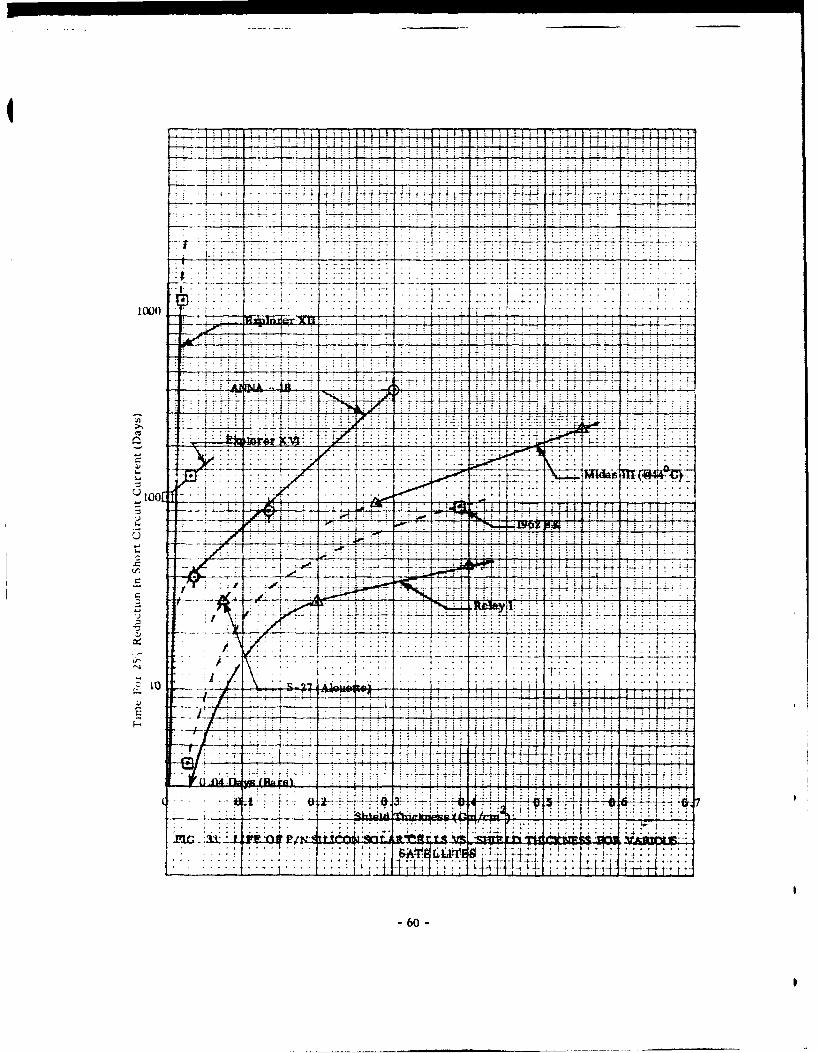
An inspection of the data showed that for the Relay- I and Ax.na I-B satellites,
which carried both n/p and p/n cells, there was a factor in the neighborhood of "bur
times longer life for n/p cells than for p/n celils under shield thicknesses greater than
- 55 -
• iii[ k m |_,S

TABLE V- I
ORBITAL PARAMETERS OF SATELLITES
PeriodNo. Satellite Perigee Ap0_ee Inclination (Min.) Lanch Date
1. Explorer XI 490.8 KM 1799 KM 28.80 Apr. 27, 1961
264 N.MI. 970 N.MI.
2. Midas 111 3450 KM 3510 KM 91.20 161.5 July 12, 19611850 N.MI. 1890 N.MI.
3. Explorer XII 304 KM 77,000 KM 330 Aug. 16, 1961163 N.MI. 41,500 N.MI.
4. Midas - IV 3530 KM 3760 KM 95,9o 166 Oct. 21, 19611898 N.MI. 2025 N.MI.
5. TRAAC 960 KM 1106 KM 320 105.6 Nov. 15. 1961516 N.MI. 596 N.MI.
6. TRANSIT - IVB 960 KM 1106 KM 32o 105.6 Nov. 15, 1961516 N.MI. 596 N.MI.
7. Ariel - 1 390 KM 1210 KM 540 100.8 Apr. 26, 1962210 N.MI. 650 N.MI.
8. TeltAr - I 952 KM 5660 KM 45 157.7 July 10. 1962513 N.MI. 3040 N.MI.
9. Tetrahedral 112 N.MI. 362 N.MI. 820 Sept. 17, 1962Research Satellite - I
10. Alouette (S-27) 1004 KM 1029 KM POLAR 105.5 Sept. 29, 1962540 N. MI. 554 N. MI.. 16 R E . 16 R E
11. Explorer XIV 278 KM 99.000 KM 330 2185 Oct. 21, 1962150 N.MI. 53,000 N.MI. (36.4 hr.)
12. 1962 -. &K 191 KM 5550 KM 710 Oct. 26, 1962(STARAD) 103 N.MI. 3000 N.MI.
1.03 RE 1.87 RE
13. ANNA -lB 1090 KM 1180 KM 500 Oct. 31, 1962584 N.MI. 635 N.MI. •
1.17 R E 1. 19 R E
14. Relay - I 1321 KM 7439 KM 47.5 185.1 Dec. 13, 1962713 N.MI. 4001 N.MI.
1.21 RE 2 .17 RE
-56-
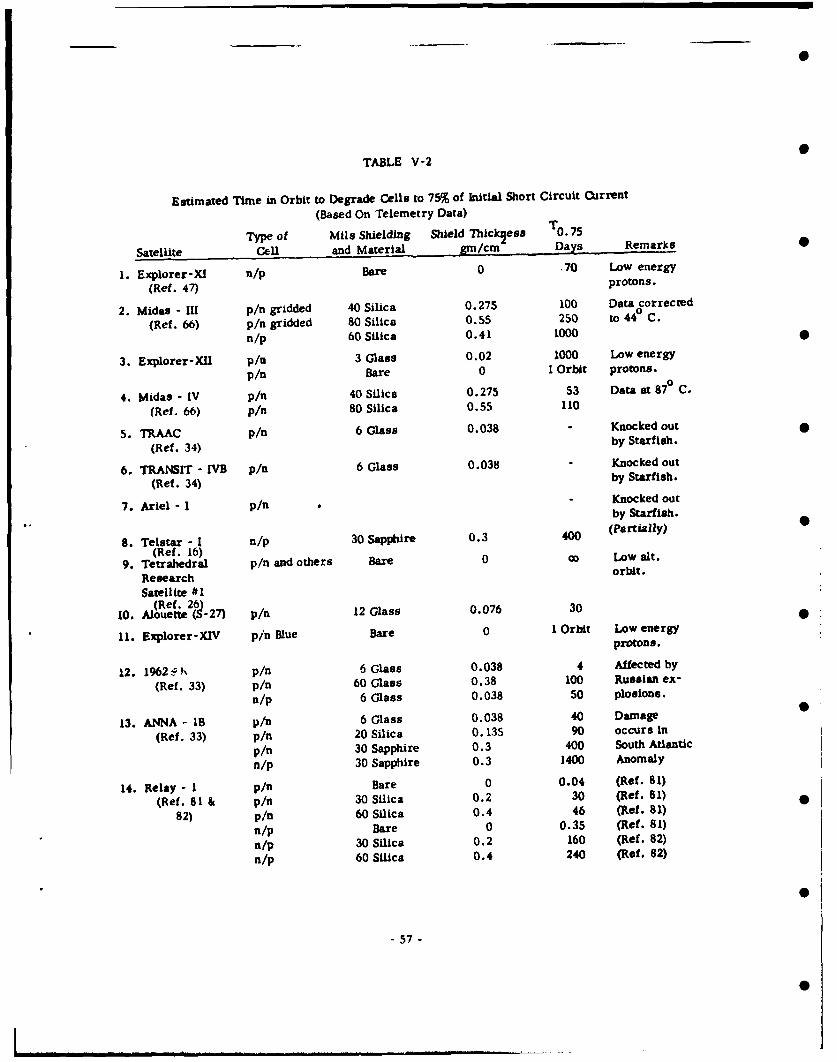
TABLE V-2
Estimated Time in Orbit to Degrade Cells to 75% of Initial Short Circuit Current
(Based On Telemetry Data)
Type of Mils Shielding Shield Thickless To. 75
Satellite Cell and Material gm/cm Days -- Remarks S
1. Explorer-XI n/p Bare 0 .70 Low energy
(Ref. 47) protons.
2. Midas - III p/n gridded 40 Silica 0.275 100 Data corrected
(Ref. 66) p/n gridded 80 Silica 0.55 250 to 440 C.
n/p 60 Silica 0.41 1000
3. Explorer-XII p/n 3 Glass 0.02 1000 Low energy
p/n Bare 0 1 Orbit protons.
4. Midas - IV p/n 40 Silica 0.275 53 Data at 870 C.
(Ref. 66) p/n 80 Silica 0.55 110
5. TRAAC p/n 6 Glass 0.038 Knocked out
(Ref. 34) by Starfish.
6. TRANSIT - IVB p/n 6 Glass 0.038 Knocked out
(Ref. 34) by Starfish.
7. Ariel - 1 p/n Knocked outby Starfish.
8. Telstar - I n/p 30 Sapphire 0.3 400 (Partly)
(Ref. 16)9. Tetrahedral p/n and others Bare 0 cO Low alt.
Research orbit.
Satellite #1(Ref. 26)
10. Alouette S-27) p/n 12 Glass 0.076 30
11. Explorer-XIV p/n Blue Bare 0 1 Orbit Low energy
protons.
12. 1962 I' p/n 6 Glass 0.038 4 Affected by
(Ref. 33) p/n 60 Glass 0.38 100 Russian ex-
u/p 6 Glass 0.038 50 plosions.
13. ANNA - lB p/n 6 Glass 0.038 40 Damage
(Ref. 33) p/n 20 Silica 0. 135 90 occurs in
p/n 30 Sapphire 0.3 400 South Atlantic
n/p 30 Sapphire 0.3 1400 Anomaly
14. Relay - I p/n Bare 0 0.04 (Ref. 81)
(Ref. 81 & p/n 30 Silica 0.2 30 (Ref. 81)
82) p/u 60 Silica 0.4 46 (Ref. 81)
n/p Bare 0 0.35 (Ref. 81)
n/p 30 Silica 0.2 160 (Ref. 82)
n/p 60 Silica 0.4 240 (Ref. 82)
- 57 -
l If g I ai If | ]a m i w • i t . • m • • - .. .

SOS
~I, +i ;;i 14: tI fl _ T i-i
__ __ Min--
.iiI fl S
.. . . . . .. . .
:fA .. . ..-. 4
. . . .. . ... .S
t o , . . . .... ...
..T. . .. . . .in~
58 --

:7- -7
10~~ ~ .. ..- i
jrrr -- f j
0.2, 0 3 0 1)/
MGOI n -.-- 4.-r q-~ -04 .:~l SbI llav litb AL i o
~~~~~~1~~~~- -- _____
VAMOU UTE UTUS
444- 7-r~ .T . .*
7-f---4-- -77 -7
44t
47.
.. . . . . . .
i a
- 60i-

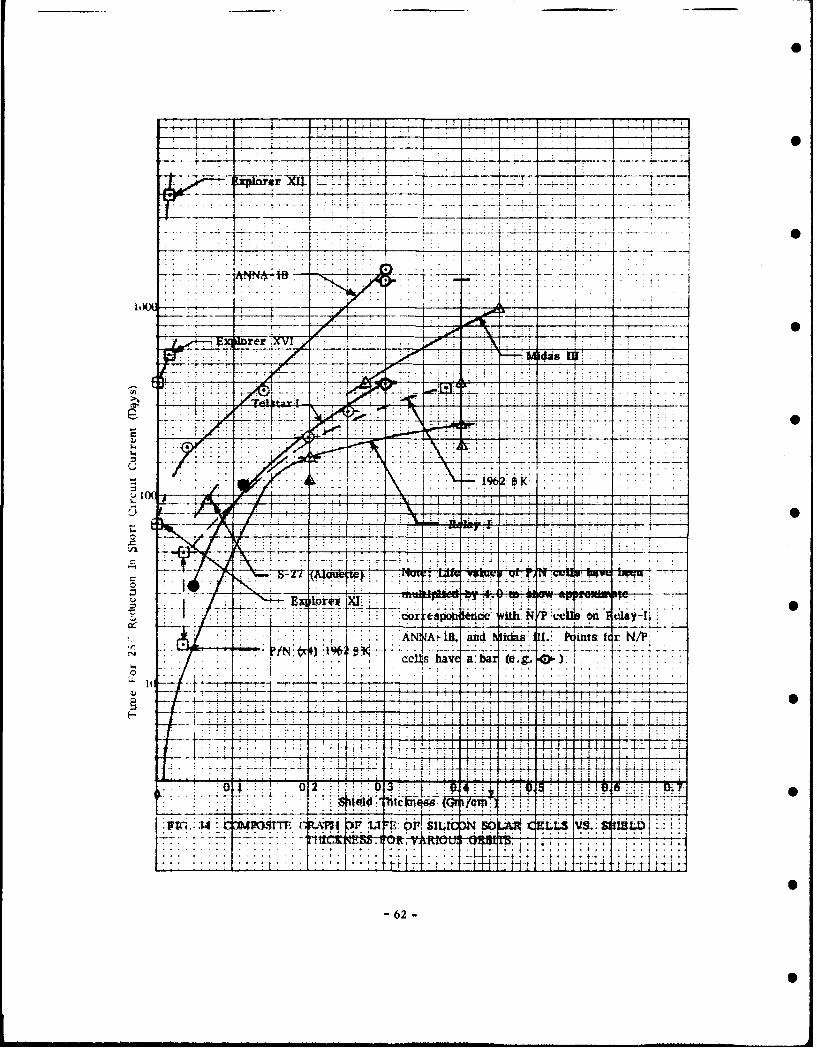
0.2 gm/cm 2 . Therefore, the data from Fig. 32 and 33 have been replotted in Fig.
by multiplying the p/n life values by the factor 4.0. It may be seen that the shape of
the resulting curve of the predicted life of n/p silicon solar cells vs. shield thickness Sappears to be a function of the particular satellite orbit, as expected, since it depends
on the electron and proton fluxes and energy spectra encountered along the orbit. The
factor of 4 difference between n/p and p/n cells is only expected to be applicable if
most of the damage is produced by protcns above about 2 Mev, where the damage 5
constants are found ,. differ by about a factor of four. It is noted that the factor of
four difference between n/p and p/n cells does not apply for the 1962 BK satellite
with thin shielding where the n/p cells appear to last more than ten times as long as
p/n cells. This fact may be due to one or both of two factors: (1) The p/n cells
degraded rapidly in four days at a time when the flux of electrons from the Russian
explosions was high, whereas the average flux during the 50 day life of the n/p cells
may have been lower, and (2) even if the average flux encountered per day were
constant in time, but the damage was produced mainly by electrons, a factor of the
order of 20 to 100 times different life is predicted on the basis of the relative damage
constants for I Mev electrons and a factor of 10 to 25 for 3 Mev electrons. Fig. 34
may be used as a fir3t approximation to estimate the life cf n/p I ohm-cm silicon
solar cells in certain orbits which have orbital parameters fairly close to those for
which the flight test data were obtained. It is seen that the most severe orbit with
respect to radiation damage is that of Relay-i, followed in order by 1962 0 K, Telstar
:, Midas-Ill and Anna-IB. The data for the Tetahedral Research Satellite No. I is S
not plotted because it showed no measurable degradation, even on bare p/n cells,
during the first 42 days, which indicates that the damage rate to solar cells Is
negligible for a satellite with an apogee of only 362 nautical miles.
- 61 -
obl -
- --7 -;;--- ~- - -
-!7 :7 7- - -f - -_
Nf . ~ -. -.. ..
7 - - - . . . . . .
t4- -
mm0
J bit a 0
CC!4SL
-- 4--4
- 62 -

VI DESIGN METHODS FOR SOLAR CELL POWER SYSTEMS
A. General Requirements
Some of the major factors which need to be considered in designing a solar cell
power system for operation in a radiation environment include:
1. The severity of the radiation environment expected in the proposed orbit.
2. The availability of radiation resistant solar cells (e.g. n/p I ohm -cm
silicon cells, higher resistivity n/p cells, or graded-base cells).
3. The thickness of shielding which can be used within the weight limit, or the
increased area of cells which can be used to produce the required power
within the area-limit. (Generally a tradeoff optimization study is desirable.)
4. The expected range of operating temperatures for the solar cells, which
affects the selection of the solar cell operating point (the voltage per cell or
the load resistance).
B. Selection of Type of Solar Cells S
Gent -ally If a proposed satellite is to spend an appreciable fraction of its time in
the altitude zone between about 1000 km and 10,000 kin, it will be necessary to use
radiation resistant n/p silicon solar cells in order to attain reasonable life. In other
ca es there may be an economic advantage In using p/n cells unless production quan-
tities of radiation resistant cells become available at equal cost. There is evidence that
n/p silicon cells with a base resistivity greater than I ohm-cm and also graded-base
(drift-field) cells are more radiation resistant than I ohm-cm cells. Therefore, it is
expected that production quantities of such cello will become available for use in extreme
environments. Solar cells of gallium arsenide, cadmium sulfide and other materials are
still in the experimental research stages.
C. Degradation Rates in Particular Orbit, as a Functton of Sn.ield Thckness
For certain orbits which are very similar to those of the satellites discussed in
Section IV, an approximation of the time for silicon cells to degrade by 25% in short
circuit current can be obtained by reference to Fig. 32, 33 and 34. For degradations
greater than 25%, which are of interect in overdesigning the total cell area. it may be S
- 63 -
n i i I m " m " +S

assumed that the short circuit current degrades by approximately 20% per decade in
time. This is a good approximation only if the radiation flux encountered per day is
constant, or if the time for 25% degradation is long compared to the period for apogee pre-
cession (the apogee precession period for Anna - IB is 120 days). If one designs for 45%
degradation in short circuit current, the life will be extended by a factor of 10 as corn -
pared to 25% degradation. It is clear that the use of area overdesign can be a potent
method of extending solar cell life. It may be preferable in many cases to increase the
number of solar cells used, rather than increase the shield thickness in order to obtain
the required power at the end of life.
D. Calculation of Solar Cell Degradation Rates 5
A procedure which can be used to estimate solar cell degradation in a particular
orbit is outlined below. The procedure given for calculating electron damage is only
applicable for a fission electron spectrum, which is approximately correct for orbits
in the region of the Mcdlwain L parameter less than 2 (an altitude of 4000 miles at the
magnetic equator). For a more general case,changes of the electron energy spectrum
along the orbit should be included in the computation.
a. Select a value of the initial diffusion length L 0 of the solar cells, typically
about 120 microns (0.012 cm) for n/p one ohm-cm silicon cells.
b• Assume an allowable degradation for the short circuit current or maximum power
and determine the final value of diffusion length L from Fig. 15 or 19
using the curve corresponding to short circuit current under space sunlight S
with the appropriate value of L0 .
c • Calculate the allowable change in (I/L) which corresponds to the final short
circuit current:
L 0 (12)
d . Calculation of Proton Damage Rate
1. Choose an energy distribution for the protons which is applicable to the
orbit and express the flux per unit energy interval in the form:
0(E) = I e -EE
-64-
This equation should apply over the range from EI. which is the minimum
proton energy capable of penetrating the assumed shield thickness as given
by Fig. 35 , up to approximately E2 = 200 Mev.
2. Use a proton damage coefficient applicable to the solar cell base material
as shown in Fig. 1i or 12.
3. Calculate the average damage integral per unit time:
-6 = (I/L 2 1 f 2 Kp(E) p (E, t) dE dt (11)p t t EI
where E, is the minimum energy that will penetrate the shield as deter-
mined from Fig. 35 . The integral with respect to time may be approxi-
mated by breaking the proton belt into several regions in B-L coordinates
and calculating the time spent in each region, taking into account orbit
regression and precession of the orbital apogee. In order to calculate
the average damage rate, the time t should equal one period of preces-
sion of the apogee, unless it is desired to predict the degradation more
precisely by integrating from the expected initial orbital parameters.
e. Calculation of Electron Damage Rate
1. Assume an energy distribution for the electrons encountered along the S
orbit, (e.g. a fission spectrum for orbits passing through the artificial
electron belt at values of the McIlwain L parameter less than 2) and
calculate the average omnidirectional flux of fission electrons per unit
time (cpF ).
2. Refer to Rosenzweig's curve of equivalent I Mev electron flux per omni-
directional fission electron for the assumed shield thickness and solar
cell type (Fig.36 ) and read off the ratio R of equivalent 1 Mev integrated
electron flux per unit omnidirectional fission electron flux. Calculate the
equivalent average I Mev flux for the orbit:
6El =
- 65 -
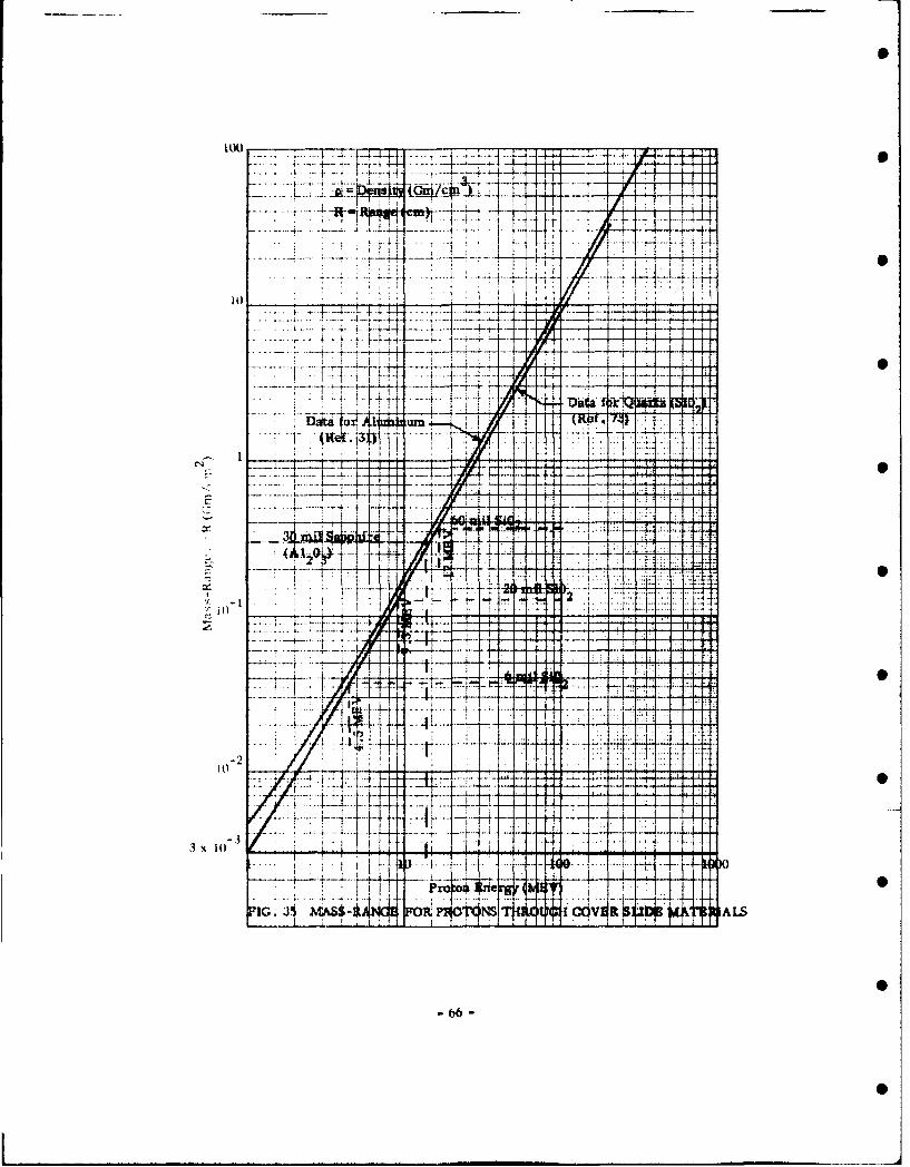
100 .- . - - - ---- ... ---
T- I
T-* ~ ~ ~ .. .....~ - '-- -4 -
JIF I4 I- i I I
fri-i
-- 2
14 T
3 x 1S 0L
IG .31 MA$t-A RPROC N L
- 66 -

+ 4
ItI
. . ... . .
IVI
I.X i . .. .i~ t .II .h .2 & . .t. .-
Pt t. 0 &1iir Ctili 1: nOl Ep troiii
:FoR66Pizw4I.74V
-67~ -
f. Read the KE l value for 1 Mev electrons from Fig. 8 for the type of solar
cell base material used, and calculate the average electron damage rate
in the orbit:
DE = K( EI (13)
This has the units of change in I/L 2 per unit time.
g. Calculate the average damage rate:
DT = D +DE (14)
where D is from Step D-3 andD E is from Step F.
h. Solve for solar cell life to the assumed final value of short circuit current
from: 2fo:T = A (IlL 2) (15)
T
where [A (I/L 2 )] is from Step C and DT from Step G.
E. Sample Calculation of Radiation Damage in Equatorial Orbits
1. Calculation of Proton Damage -
It is assumed that the proton spectral flux is given by McIlwain and Pizzella.
(Ref. 100):
0 (E) 10 e- E/E 0 (16)
-5.2where E0 = 306 L (Mev) (17)
L - McIlwain's parameter
For a satellite at an altitude of 2000 miles (half an earth radius) L = 1.5 and E0 = 37.3
Mev. The value of 1 is found by normalizing to an integral flux above 40 Mev. of
2 x 10 4protons/cm - sec, as given by O'Brien (Ref. 104):
40
2 xe10OdEotns/cmI0 :J 0 e -E/E 0 d =2x10 (18)
or I0 = 1570p/cm - sec -MevThe radiation damage to n/p 1 ohm-cm silicon solar cells covered by 30 mils of
sapphire shielding on the front and with infinite back shielding will be estimated. The
- 68 -
i •

0
proton damage coefficient is assumed to be
K = A/EP
where A = (1.5 x 10. ) for E < 60 Mev (19)
K = B = 2 .5x10- 7 forE>60Mev
It is assumed that the energy spectrum and flux of protons behind the shield is the same
as on the outside of the shield except that the low energy particles are stopped by the
shield. This assumption is equivalent to assuming that the lower energy and therefore
higher damage coefficient for those protons which penetrate the shield is just compen-
sated by the fact that an omnidirectional flux of incident protons is strongly absorbed
at small angles of incidence so that only protons within a certain entrance cone can
penetrate. This assumption is conservative in that it somewhat over estimates the
damage produced by protons which have energies slightly greater than that required to S
penetrate the shield. (Compare Rosenzweig's calculated results as shown in Fig. 37
The change in inverse squared diffusion lengh for the cells is calculated from:
-A(/L2 = -- f p(E) K (E) dE (20) •E
cwhere T = time of exposure, seconds
2E = cutoff energy = 14 Mev for 30 mil sapphire (0.3 gn/cm2 )
cor S
I T 60(I/L2 $ AE-e-/E0 dE + Be/ 0 dE (21)
JE 60c
EIf we let x
E0
Then10T rx60 I
(l/L') --2 AfX6 - -xdx +BE 0 f e X dx (22)x c x60
14 60 Swhere x =--0 6 Ec E60E0
and e X dx e 6 0/E 0 (23)x60 S
o 69 -

.. . . .. . . . . . . . . . . .. . -f- - + H i .. . f'!
::: ~ ~ T ::t -V 4z±~.-:- :
7~-,.- 7 rfIz -I il
I J.:I
Proon n (MEV)
I 10 -- 1
1i I-Ht4 fS
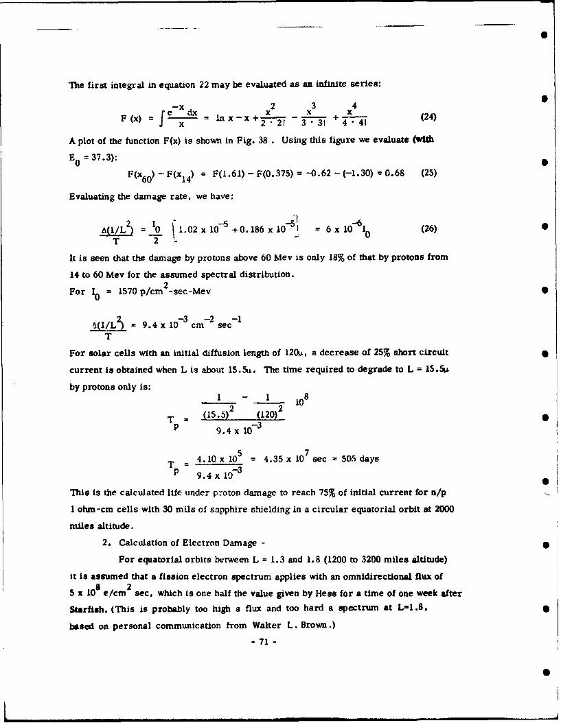
The first integral in equation 22 may be evaluated as an infinite series:
-x 2 3 4 •
re- dx 2 x 3 x4F(x) = e = lnx-x+ 2 . 2 33f +44" (24)
A plot of the function F(x) is shown in Fig. 38. Using this figure we evaluate (wtlh
E0 = 37.3):
F(x 6 0 ) - F(xl 4 ) = F(1.61) - F(0.375) = -0.62 - (-1.30) = 0.68 (25)
Evaluating the damage rate, we have:
(/L2= 0 1 .02 x 10- 5 + 0. 186 x =0 : 6 x 10 -6 (26) ST 2 0
It is seen that the damage by protons above 60 Mev is only 18% of that by protons from
14 to 60 Mev for the assumed spectral distribution.
For I0 = 1570 p/cm 2-sec-Mev S
(1/L 2 )= 9.4 x 10- 3 cm- 2 sec- 1
T
For solar cells with an initial diffusion length of 120L, a decrease of 25% short circuit •
current is obtained when L is about 15.5u. The time required to degrade to L = 15.5
by protons only is:1 - 1 108
T = (15.5) (120)
9.4 x 10 3
5 74.10 x 10 = 4.35 x 10 sec = 505 daysT =
p -3P 9.4 x 10
This is the calculated life under p-oton damage to reach 75% of initial current for n/p
1 ohm-cm cells with 30 mils of sapphire shielding in a circular equatorial orbit at 2000
miles altitude.
2. Calculation of Electron Damage -
For equatorial orbits between L = 1.3 and 1.8 (1200 to 3200 miles altitude)
it is assumed that a fission electron spectrum applies with an omnidirectional flux of8 25 x 10 e/cm sec, which is one half the value given by Hess for a time of one week after
Starfish. (This is probably too high a flux and too hard a spectrum at L-1.8,
based on personal communication from Walter L. Brown.)
-71 -
444L
. .. . . . .
4
7 1 4
~ + .4- i 4
72 H+ t-ij- - -
From Rosenzweig's data (Fig.36) the conversion factor from omnidirec-
tional fission electrons to equivalent normal incident I Mev electrons is 0.37 for a
shield thickness of 0.3 gm/cm2 on n/p cells.
The change in I/L2 per I Mev electron is found to be approximately
Kx 1 = 1.64 x 10- 10El -'-2.5 x 10¹⁵
(Fig. 8 shows K El = 1.7 x 10⁻¹⁰ at I Mev)
The average electron damage rate is:
D K-10 8E KEl El = (1.64x ) (0.37)(xl 0)-2 -1
D E = 0.0303 cm sec
The time to degrade the cells by 25o, considering only electrons is:
TE _ . 4.1Ix 10 5-
S= 00-303 5 1.35 x 10⁷ sec = 156 daysDT
3. Calculation of Combined Effect of Electrons and Protons -
The total damage rate is
D =D +D + (27)~~(/2 )~ l/ 2T E P TT = TE + T (27)PI
from whichI I I
T T + Tp (28)
or TE TpT = T+Tp(29)T 7- .+T
- P
The life under combined electrons and protons is then
T = (156) (505) = 119days
T - (156 +505)
This is the calculated life to reach 75% of initial current for n/p I ohm -cm
silicon cells with 30 mils of sapphire shielding in a circular equatorial orbit at 2000
miles altitude.
- 73 -
i i l ti |" m:• a .

Similar calculations have been made for other altitudes using the proton flux
map shown in Fig. 30 and the results are plotted in Fig. 39. It is seen that the
damage rate by protons increases with altitude and has not reached its maximum at
an altitude of 5000 kin, above which the absolute value of proton fluxes are not well
defined. This effect is due to the increasing fluxes of protons with energies slightly
above the 14 Mev shield cutoff energy which are encountered with increasing values of Sthe Mcllwain L parameter.
The solar cell life of 80 days calculated for an altitude of 5100 km may be com-
pared with the observed life of 190 days interpolated from Relay-i flight test data.
One may conclude that the Relay- I damage rate is equivalent to spending about 40% of 0
its time at the most damaging point calculated, namely at 5100 km altitude at the
equator. Actually Relay spends considerable time at larger L values than 1.8 where
it encounters many low energy protons and it also passes through the artificial electron
belt. Therefore, a computer calculation would be required after the fluxes and spectra 0
are better defined in order to compare predicted with observed degradation rates.
F. Comparison of Calculated and Observed Damage on S-27 Alouette.
The Alouette is in approximately a 1000 km circular polar orbit for which Hess
(Ref. 39) has calculated an omnidirectional flux of fission electrons of 2 x 10 per
day at a time of one week after Starfish. Alouette was actually launched on Sept. 29,
1962, nearly three months after Starfish. For blue-shifted p/n solar cells with212 mils (0.076 gm/cm ) of glass shielding, Rosenzweig's conversion ratio from
Fig. 36 is found to be 0.37, so the equivalent I Mev flux is 0.74 x 10 e/cm day.
The damage coefficient for p/n cells at 1 Mev is selected from Fig. 9 to be
1.22 x 10"- 8 and the change in I /L 2 to produce 25% reduction In short circuit current5 -2
is taken as 4. 1 x 10 cm . Therefore, the time to reach 25% reduction In short
circuit current under electron damage is
T A(l/L)2TE Kp
4.1 x 10S
T = - 45 days(1.22 x 10- ) (0.74 x 101)
This is probably an underestimate of "electron life" because of decay of the artificial
belt.
- 74 -

410 -T---7-
d ao;ags Oteis
. . . . . . . .
jrtttea I~e rtn mg-alyIIi
. .-. . . ... . .
100 -. . ~ .L ~ .... ...
.. .q :. .... .... .. . .. ....u .. ..M. . ...
...-. ... . .---.-. . . ........q 1M R.~R ~ D4 TIC URN/uINx. V. ~. .... A ... R!~
'nig 75
.... ... t~S

Flight test data from Alouette showed a 25% degradation after about 30 days.
The added damage sustained may be accounted for by protons encountered in the South
Atlantic Anomaly.
- 76 -
S

APPENDIX A
RADIATION EFFECTS ON SOLAR CELL COVER SLIDE MATERIALS AND ADHESIVES
A. Introduction
The prediction of solar cell power system life should take into account the
degradation of the optical transmissive properties of the cover materials. The covering
materials are generally a transparent cover slide and a transparent adhesive. The
cover slide is utilized to shield against electrons and protons, and to carry a spectrally
Selective filter. It also protects against contamination from being handled on the
ground. Investigations have been conducted with protons and electrons on various cover
slide materials and adhesives. From these studies an indication of the degradation
that can be expected in service may be derived.
B. Damage Mechanism
Cover materials are susceptible to "F" center formation from high energy •
particle fluxes. The formation of these color absorbing centers is a function of the
impurities in the material. Most color centers can be annealed out of the material
by heat, infrared radiation or visible light.
In general, the sensitivity to coloration is not fixed for a given type of engineering S
material but varies according to the impurities, lattice imperfections, strain, stoichiometry
and the prior deformation of the material (Ref. 118). When irradiation is at elevated
temperatures an equilibrium density of color centers is attained from the production and
destruction of the color centers. a
Relatively little work has been done on coloration or the coloration equilibrium
from simultaneous energetic protons, electrons and ultraviolet radiation below 3000
Angstroms in the presence of the longer wavelength components of sunlight. However,
the change in transmittance of various materials from proton and electron radiation
has been measured by F. A. Campbell of the Naval Research Laboratory (Ref. 112)
and by J. L. Patterson and G. A. Haynes (Ref. 120) of the Langley Research Center.
These data give an indication of the amount of damage that can be expected in service.
"Al -

C. Cover Slide Requirements
The most desirable materials for solar cell cover slides are those which show
the least amount of transmission degradation within the solar cell spectral response
band upon exposure to electron and proton radiation. This spectral band is typically
0.35 to 1. 1 microns, with a peak near 0.8 microns. When the spectral distribution
of space sunlight is taken into consideration, the peak energy point occurs at approxi-
mately 0.6 microns.
D. Electron and Proton Damage Experiments
Assessment of electron damage has been made by F. A. Campbell (Ref. 112 •
and 113) of the Naval Research Laboratory. Electrons of I Mev energy at a total dose
of 1016 e/cm 2 were utilized. Spectral transmittance was measured with a Beckman
IR-4U double beam spectrophotometer. The electron exposure was conducted in air,
directly under the beam of a Van de Graaff. Transmittance values for various materials
between 0.4 and 0.7 microns are summarized in Table A-I (Ref. 113).
Patterson and Haynes (Ref. 120) utilized a Radiation Dynamics No. P.E .A .-lO2accelerator with a constart beam current density of 0.03 microamp/cm . Electron
energy of 1.2 Mev was used and most of ;he samples were exposed to a total dose of15 22.7 x 10 e/cm . A 2900CK filament temperature tungsten lamp was used as the
source and the transmission efficiency was recorded as a percent change in broad
spectral band light passing through the sample to a typicd.l solar cell. The measure-
ment accuracy was 1/2%.
Measurements of changes in spectral transmission after proton irradiation
were conducted it the Naval Research Laboratory. The irradiation consisted of a
single dose of 4 x 10 p/cr.-" at an energj of 4.6 Mev. The samples were irradiated
in vacuum at a pressure of 10-4 mm Hg and the results rre 3ummarized in Table A-2.
The test data show a superiority for t' ,n Corning 7940 cpecimens as compared to
Coming 0211.
1. Silica
Two major classes of silica are synUhotic qu-:tz (or fused silica) and vapor
deposited silica. Both electron and proton damage is reported for variou.r types and
manufacturers of fused silica as shown in Tables A-I, A-2 and A-3. Electron radiation
- A2 .

C" 14
m~ ~ ~ -- N0.- V C ci
C', A6'-C y M O
- 00
v
-- C
s
0 ~ ~ ~ ~ ~ ~ e + ~S n 0 0 0
- 44'0 0 0 0 '00 0 C'~ 0 0'0 Sn o n t
W 0 u CZS ~0' N - (4 '3~0' ~ 0 9
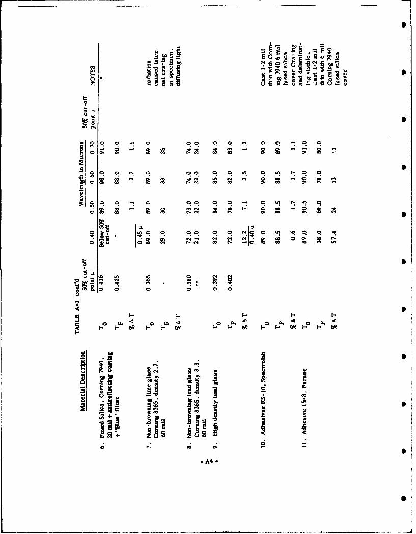
bo 0 0 F
00
0m - 0 4
In S
C; 40 00 0o m C- 0 a, cc al
v~ 00 (' c4
a SK
0 0 0
:1 a.c.. ~ 0 .0 0 106 4
5A

U))
0 1
VS
In I
4)
0 0
C14
cs
4
4 u
o .0 Inn
U0o CL.
C., I~A5

V) 0 0-
0) co co 47uo
0 n Sn - 0 -'0 0: 1.4 Go tic - l 00 00 c'o
0 ~ ~ ~ V 0 c c ~ a
0 .4
U~ 140 Qn SnC. S iwco co Go~
Snen
%.4 . l 0 0 Snco'
oo t-
< 1 4 1
C4 +C4
A6a

ASS
m m
o ~ ~ c co4 ~o -~
cc4~ 00~
1.0.
En >
CY Cl.
-- 0 -4 to
0 - 4- 0 ! to -
o ~ . -7
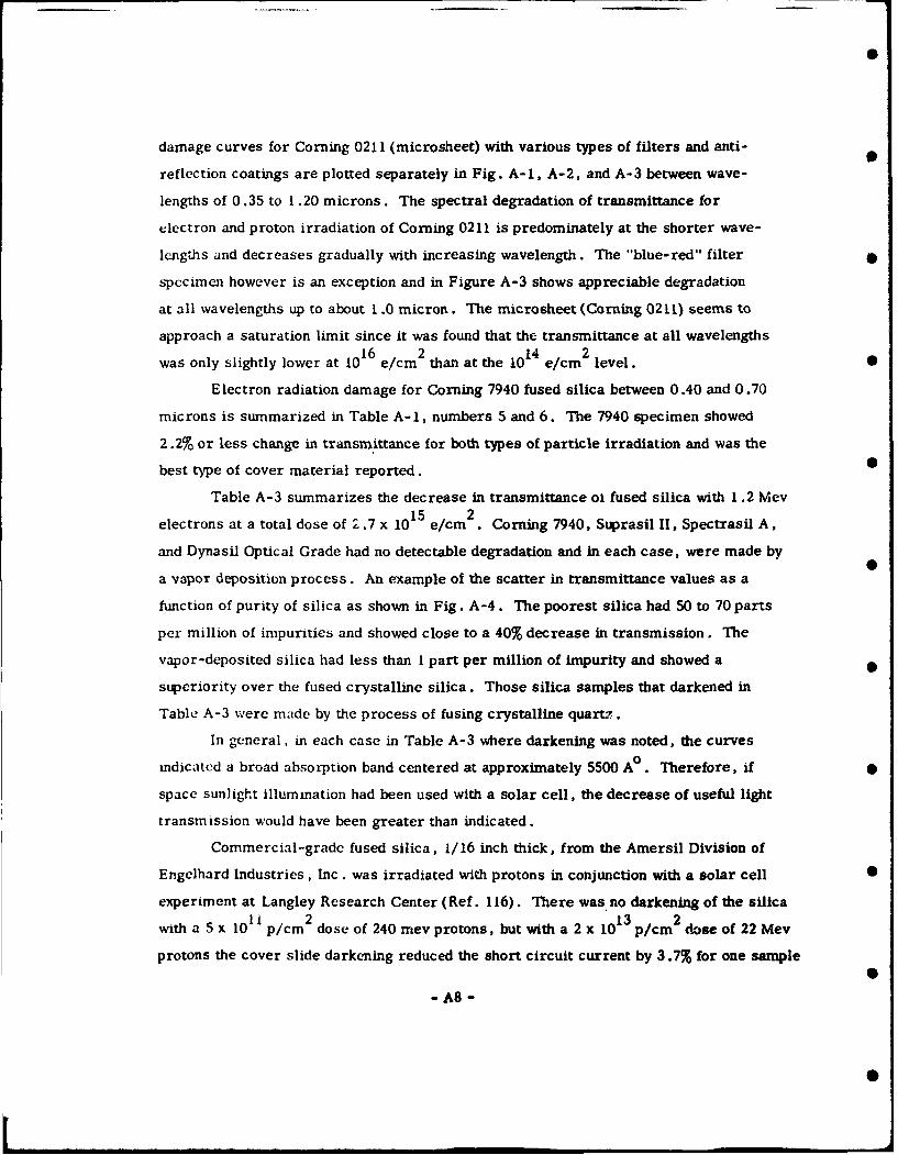
damage curves for Coming 0211 (microsheet) with various types of filters and anti-
reflection coatings are plotted separately in Fig. A-I, A-2, and A-3 between wave-
lengths of 0.35 to 1.20 microns. The spectral degradation of transmittance for
electron and proton irradiation of Coming 0211 is predominately at the shorter wave-
lengths and decreases gradually with increasing wavelength. The "blue-red" filter
spccimen however is an exception and in Figure A-3 shows appreciable degradation
at all wavelengths up to about 1 .0 micron. The microsheet (Corming 0211) seems to
approach a saturation limit since it was found that the transmittance at all wavelengths
was only slightly lower at 1016 e/cm 2 than at the 1014 e/cm2 level. S
Electron radiation damage for Coming 7940 fused silica between 0.40 and 0.70
microns is summarized in Table A-i, numbers 5 and 6. The 7940 specimen showed
2.2% or less change in transmittance for both types of particle irradiation and was the
best type of cover material reported. 0
Table A-3 summarizes the decrease in transmittance o1 fused silica with 1.2 Mev15 2
electrons at a total dose of 2.7 x 10 e/cm . Corning 7940, Suprasil II, Spectrasil A,
and Dynasil Optical Grade had no detectable degradation and in each case, were made by
a vapor deposition process. An example of the scatter in transmittance values as a
function of purity of silica as shown in Fig. A-4. The poorest silica had 50 to 70 parts
per million of impurities and showed close to a 40% decrease in transmission. The
vapor-deposited silica had less than I part per million of impurity and showed a
superiority over the fused crystalline silica. Those silica samples that darkened in
Table A-3 were made by the process of fusing crystalline quartz.
In general, in each case in Table A-3 where darkening was noted, the curves
indicated a broad absorption band centered at approximately 5500 A0 . Therefore, if S
space sunlight illumination had been used with a solar cell, the decrease of useful light
transmission would have been greater than indicated.
Commercial-grade fused silica, 1/16 inch thick, from the Amersil Division of
Engelhard Industries, Inc. was irradiated with protons in conjunction with a solar cell 5
experiment at Langley Research Center (Ref. 116). There was no darkening of the silica
with a 5 x 101 p/cm2 dose of 240 mev protons, but with a 2 x 10¹³ p/cm2 dose of 22 Mev
protons the cover slide darkening reduced the short circuit current by 3.7% for one sample
- A8 -
0

... . . .. . . . . . . .*
............
. . . .....
*~~~ . . . . ..................
. .4 . ..
. . . . . . . . . . .S
. . .. . . .. .
. . . .. .j ..-.
. . . . . . . . . .
._ . . . . . . .4 . .
-A9-
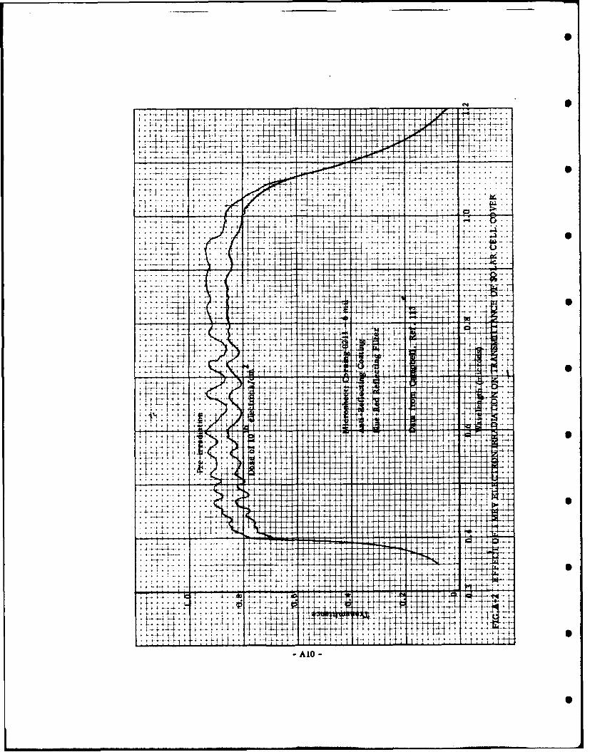
*~.. ..... * I
1 -4 4
- - 4 -
-~4 AI -
4 +1 t t -S

S
t ~ ~ ~ ~~ T - T '. - -
-4 •4
-'---r -..... r rrnr .T-i ... ..
r. *-4-" '• • L1S -•
II:.:: tJ~T:24 - rt 4 t
+1-,,
. . . . . . . ... .. . .. . . . . . . . . . ., . . . . ..
........ . . ......... 4. .- S
........ ....... .... .. .. . ..-....... .
.. . . . . . . . . ... .
.-
+ 5 .
. . . . . . . . . . . . .., , .. . . . .. . . .
4-i4-
-f- -r 4
.1'1- 4-
- -1
+ 4 I
. .* . .z 9 ..-. .t t 1
* .ll
at .\.'.. .
1 . t
iI .
.. ... ... .
.. .. . .. . .
.. . .... ...
. .. . .. . .. . ..
and 7.6% for a second. The solar cells were 8% efficiency p/n cells and the light
source was a lamp with a tungsten filament operating at 2900°K with a 1-inch-thick
water filter.
Tests of ordinary quartz shielding by Kallander and Weller (Ref. 119) with152 San integrated flux of 6 x 10¹⁵ 1 Mev electrons per cm also showed considerable
darkening, which indicates that impure silica is to be avoided.
2. Glass
Typical varieties of glass are very susceptible to radiation damage as shown
in Table A-3. The ordinary soda lime plate glass degraded in transmittance by 26.0%is 2
with a dose of 2.7 x 101 1.2 Mev electrons/cm . Some protection is available with
the addition of trivalent cerium which tends to neutralize the color centers, thereby
reducing the absorption.
3. Sapphire
Artificial sapphire has been used as a cover shield material for solar cells
(e .g. on Telstars I and II). The Langley Research Center irradiated a cover shield
made of artificial sapphire from the Linde Company, with 1.2 Mev electrons at a total Si5 2dose of 2.7 x 10 e/cm . With this flux, no decrease in broad band transmittance was
observed. This material as shown in Table A-3 was the only material other than
vapor-deposited silica that suffered no measurable decrease in transmittance.
4. Adhesives 5
Adhesives are often utilized to bond the cover shield to the face of the solar
cell. The adhesive requires dimensional stability, transparency, high electrical
resistivity, long term adhesion and chemical compatibility with the solar cell. The
primary concern to date has been vith the change in transparency under proton, electron
and ultraviolet radiation. The effect of Cobalt 60 gamma radiation on the resistivity
of an Epoxy adhesive is reported by Kallander and Weller (Ref. 119). The surface
resistivity decreased to 109 ohm-cm at a dose of 2 x 10⁸ Roentgens.
F. A. Campbell of the Naval Research Laboratory has measured the change
in spectral transmission of adhesives Dow DER-332, Epocast 15-E and Spectrolab ES-10
with electron irradiation. The adhesives were cast 1-2 mils thick in the same method
as used to cement cover slides to solar cells. The adhesives ES-I0 and 15-E were cast 5
- A13 -
under a 6 mil Corning 7940 fused silica cover and the DER-332 under a 66 mil fused
silica cover. The additional shielding did not help the DER-332 and it degraded more
than the ES-10 adhesive which was less well protected. The data are tabulated in
Table A-1, nurb. 10,11 and 12. The ES-10 shows a marked superiority and did not
degrade more than 2%. The 15-E showed a decrease in transmission with each successive
electron exposure, particularly at the shorter wavelengths. Crazing and delamination
were also visible in this specimen which would diffuse the spectrometer light. there-
fore giving a lower transmissivity reading. However, this diffused light may stillS
be utilized by a solar cell.
E. Conclusion
The materials tested which indicated a superiority by showing minimum
darkening with energetic electrons are Corning 7940 of Corning Glass Works,
Suprasil II and Optical Grade Silica of Engelhard Industries, Inc., Spectrasil A
of Thermal American Fused Quartz Co., GE 104 of General Electric Co., Dynasil
(Optical Grade) of Dynasil Corporation, and synthetic sapphire of the Linde Company.
The material tested with the least change in transmittance for 4.6 Mev protons was S
Corning 7940. The adhesive tested with the least change in transmittance under
electron irradiation was the Spectrolab ES-l0 specimen.
- A14 -
S

I
APPENDIX B
SPACE RADIATION EFFECTS ON TRANSISTORS & DIODES
A. Introduction
In addition to solar cells, the semiconductor devices of primary concern with
respect to radiation damage are transistors and diodes, which also depend on diffusion
of minority carriers for their operation. Primary consideration will be given to those
types of transistors and diodes associated with solar cell power systems. In some
applications, power regulation components, such as diodes, Zener diodes and transistors,
have been located on the solar panels or satellite skin where they are exposed to space
radiation with a minimum of shielding. Even when located inside a satellite, it is found
that transistors and diodes having gas-filled cases, can be seriously affected.
8. Radiation Damage Mechanisms
The primary radiation effects to transistors and diodes which are of concern in
satellites are (1) the surface effects associated with ionization of gas in the device
enclosure, and (2) the permanent damage to the minority carrier diffusion length
produced by introduction of lattice defects. The effect of injection of electron-hole
pairs by Ionization in the semiconductor material is of major significance only under
extremely high flux conditions, such as the transient neutron and gamma radiation
produced by a nuclear explosion, and therefore will not be discussed here.
C. Surface Effects of Radiation
For transistors and diodes which have a gas-filled enclosure, the rather complex
effects of ioniz.-:i-n cA' the gas interacting with the surface of the semiconductor can
produce changes i i performcnce parameters at radiation doses as low as 104 Roentgens.
Such a dose may be accu:nuhted in a period of hours to months in the magnetosphere,
depending on the aniount of shielding. Therefore it is important to select transistors
which are least sensitive to this effect.
Reference should be made to the papers by Peck, Blair, Brown and Smits (Ref. 141
or 142) for a detailed discussion of this surface effect which occurs in transistors under
a combination of a radiation environment, a bias voltage, and a gas in contact with the 0
-B1 -

surface. The effects observed depend on the junction bias, the envelope voltage, and in
many respects on the total radiation dose, rather than dose rate. Upon removal of
the bias voltage or the radiation field, a device tends to recover.
It has been found that large variations in test results are observed between
units of the same type made by the same manufacturer.
It was found that some devices can be screened for sensitivity to radiation by
means of a short-time, high level radiation dose, with correlation to the subsequent
behavior under low-level radiation exposure.
The data generally indicate that transistors and diodes in evacuated cases and
planar units (with protection over the semiconductor surface) are least affected by
ionizing radiation (Ref. 143). By the use of evacuated cases, the dose at which a
noticeable increase in the collector reverse current (Ic0) occurs can be extended to
the range of 106 to 107 Roentgens as seen in Fig. B-i (from Ref. 142).
D. Degradation of Diffusion Length in Transistors
Of the changes in semiconductor properties affected by radiation, changes
in minority carrier diffusion length (or lifetime) a'.e the predominant cause of permanent
damage in transistors and diodes. A large amount of testing has been conducting on •
germanium and silicon devices in neutron and gamma ray fluxes and damage coefficients
have been dctermined. However, there is no clear correlation which permits the use
of data determined in neutron or gamma ray fluxes to predict damage by protons or
electrons (Ref. 125). 0
The transistor parameter which is affected most seriously by a degradation of
the diffusion length is the common emitter forward gain (hFE), which is also called P.
Bilinski et al (Ref. 125) give the following equations for correlating transistor performance:1 = 1
h - hI + KFE FEO
where h FEO = initial current gainhFE = current gain after bombardment •
t average transit time of minority carriers in base
= integrated flux
K lifetime damage constant
- B2 -

100_
TypeA Dry Air + Getter - .
S10
Type eN +He> 1.0o ...
. /// / Type A ,
01
10 10 100 (S 1 7 IO0
8Integrated Gamma Dose (R)
85(Radiation Dose Rate 8 .5 x 10 rads/hr)
FIG. B-I EFFECT OF GAMMA RADIATION ON COLLECTOR REVERSE
CURRENT OF EVACUATED AND GAS-FILLED SILICONTRANSISTORS
"83"

and K is given by
q I l K
T q'0 T
0
The average transit time of minority carriers in the base region of the transistor
is given by:
For a uniform bas,- W-2L 2 nf ab
For a linear graded baseW2
4L V7 n ab
where W = base widthL = minority carrier diffusion Length
f = alpha cutoff frequency
The above expressions agree well with experiment, except in the case of P-N-P
germanium transistors where the effect of depletion layer widening of the collector
region is appreciable. (This case has been treated by Easley and Dooley, Ref. 129).
Except in this case, the lifetime damage constant for germanium and silicon transistors
is given by: 2nf
KT=(h FE0 h F E ) hFEO FE
K is related to the diffusion length damage constant K L by K = DK L
where D is the diffusion coefficient for minority carriers.
Measurements of germanium and silicon transistor performance after proton
irradiation at 22 and 240 Mev have been reported by Hulten, Honaker and Patterson of
the NASA Langley Research Center (Ref. 42). Tests with 40 and 440 Mev protons are
reported by Honaker and Bryant (Ref. 132).
An attempt to correlate the Langley data on transistors in terms of lifetime
damage coefficients for the base materials was made by Bilinski, et al (Ref. 125).
However, the data showed considerable scatter, some values for p-type silicon being
an order of magnitude smaller than the damage coefficients measured for p-type silicon
in solar cells by Bell Telephone Laboratories.
-B4 -
It is apparent that further careful research is required to obtain quantitative
data on which to base predictions of the degradation of transistor performance under
penetrating proton radiation. However, general rules and guidelines for the selection
of transistors can be derived from available test data.
E. Selection of Transistor Type
There is evidence that germanium transistors are more resistant to proton
(and neutron) radiation than are silicon transistors which are designed for the same
alpha cutoff frequency. Also the sensitivity to radiation damage is much less for
transistors with a narrow base width and a high alpha cutoff frequency. There is some
evidence that germanium P-N-P types are more resistant than N-P-N types. (This is
found to be true under neutron radiation, Ref. 124). Therefore one may conclude that
the most radiation resistant transistor should be a P-N-P germanium type with a thin S
base region and correspondingly high alpna cutoff frequency. In order to minimize
surface effects, the transistor should be vacuum encapsulated. If the temperature
environment dictates the use of silicon, the cutoff frequency should be high. There
does not appear to be a clear distinction between the resistance of P-N-P and N-P-N
silicon types, although, on the basis of solar cell experience, one would expect the
N-P-N type to be superior under proton and electron irradiation.
Unless care is taken to avoid surface effects, a transistor may fail by increase
in collector reverse current at a total radiation exposure much lower than that required
to degrade the current gain.
F. Diodes
The behavior of diodc and rectifiers, and Zener reference diodes in neutron
and gamma ray fields has been reviewed by Reid (Ref. 64). In general, there was
often an initial change in ,.he reverse characteristic of diodes (which was probably
attributable to surface effects), followed by a degradation of the forward characteristic.
The life determir.cd by the allowable increase in forward impedance can be greatly S
increased by using a diode of narrow base width. A factor of 10 reduction in base width
yields an increase in radiation tolerance by a factor of about 100.
In comparing alloy and diffused diode structures, Huth (Ref. 133) observes that
the diffused structure markedly improves radiation behavior. Reid (Ref. 64) concludes 5
-B5 -
that the optimized configuration of a silicon diode for use in radiation fields would
consist of a diffused p - i - n structure with the minimum base thickness consistent
with peak inverse - voltage requirements. Based on present knowledge of surface
effects, it appears that vacuum encapsulation would be desirable.
G. Shielding Against Space Radiation S
in estimating the life of transistors and diodes in a space environment, it must
be recognized that surface effects are dependent on the ionization rate produced by
protons, electrons and Bremstrahlung (x-rays) in a gas filled device enclosure, whereas
the degradation of minority carrier lifetime depends on the flux and energy spectrum of 0
those penetrating electrons and protons which have sufficient energy to produce lattice
displacments (> 145 Kev for electrons and > 98 ev for protons in silicon).
The severity of the surface effect problem is critically dependent on the flux
and energy spectrum of the electrons in the artificial belt which are predominant over
protons in determining the ionization rate (RADS/day) in gas filled devices (Ref. 143).
Fortunately, there is evidence that the electron energy spectrum is now much softer
(relatively fewer high energy electrons) than a fission spectrum, at least in the upper
regions of the artificial belt (Ref. 126). However, it appears desirable to use evacuated
devices where possible and to locate any gas-filled devices inside a satellite to take
maximum advantage of available shielding, if operation is required in the artificial
electron belt. Gas-filled devices should be carefully selected and tested for sensitivity
to surface effects.
If trnsistors or diodes are used outside the satellite shell, they should be
evacuated and have protection by at least the same thickness of shielding as the solar
cells. For example, at least 0.3 grams/cm 2 of shielding (45 mils of aluminum) is S
desirable for a satellite orbit like Telstar or Relay which passes through the inner
proton and electron belts.
B
- B6 -
S

VII REFERENCES
A. References on Radiation Effects on Solar Cells
1. Anderson, R. E. D., Hake, E. A. and Feldman, D., "Telstar Satellite PowerSystem"; Presented at ARS Space Power Systems Conference, Santa Monica,Calif., ARS Paper 2503-62, Sept. 25-28, 1962.
2. Anderson, R. E. D., Meszaros, G. W. and Ciccolella, D. F., "The SatellitePower System (Telstar)"; Bell Laboratories Record, Vol. 41, No. 4, pp. S143-150, April 1963.
3. ASTM Special Technical Publication 330, "Space Radiation Effects on Materials",Published by Amer. Soc. for Testing and Materials, 1916 Race Street,Philadelphia 3, Penn., 1962.
4. Baicker, J. A. and Faughnan, B. W., "Radiation Damage to Silicon Solar Cells"; SSummary Report on Contract NAS 5-457, July 31, 1961.
5. Baicker, J. A. and Rappaport, P., "Radiation Damage to Solar Cells"; USAECReport TID-7652, pp. 118-135, Nov. 1962.
6. Baicker, J. A., Faughnan, B. W. and Wysocki, J. J., "Radiation Damage toSilicon"; Third Semiannual Report on Contract NAS 5-457, RCA Laboratories,Princeton, N. J., April 15, 1963.
7. Baicker, J. A. and Faughnan, B. W., "Radiation-Induced Changes in SiliconPhotovoltaic Cells"; J. App. Phys. 33, 3271 (1962).
8. Bell Telephone Laboratories, "NEEP, Nuclear Electronic Effects Program";Fifth Triannual Technical Note, WADD-TN-61-17, Nov. 15, 1960.
9. Berger, M. J., "Quarterly Status Report - April 1, 1963 through June 30, 1963on NASA Contract R-80", (Monte Carlo calculation of electron transmissionthrough sapphire shields), National Bureau of Standards, June 30, 1963.
10. Berman, P., "Radiation Damage in Silicon Solar Cells Using 750 Key and S2 Mev Electrons"; Transitron Electronic Corp. Technical Reprint, pre-sented at Meeting on "Radiation Damage to Semiconductors by High EnergyProtons", NASA, Washington, D. C., Oct. 20, 1960.
11. Bilinski, J. R., Brooks, E. H., Cocca, U., Maier, R. J. and Seigworth, D. W.,"Proton-Neutron Damage Correlation in Semiconductors"; General Electric SCompany, Radiation Effects Operation, Syracuse, N. Y., Prepared underContract NAS 1-1595, June 1962.
12. Billington, D. S. and Crawford, H., Jr., "Radiation Damage in Solids";Princeton University Press, 1961.
R1

13. Bobone, R. and Merchant, B. W., "Predicting Damage to Silicon Solar CellsSubject to Complex Radiation Spectra"; AIEE Paper No. CP-62-1279, 1962. 0
14. Brancato, E. L., "Determination of Significant Differences in Solar CellExperiments"; Presented at IEEE Photovoltaic Specialists Conference,Washington, D. C., April 10-11, 1963.
15. Brown, W. L., "Damage to Semiconductors from Space Radiation", Presentedat Amer. Rocket Soc. Space Nuclear Conference, Gatlinburg, Tenn., May 3,1961.
16. Brown, W. L., "Radiation Damage Effects on Teltar-I", Presented at IEEEPhotovoltaic Specialists Meeting, Washington, D. C., April 10-11, 1963.
17. Carter, J. R. and VanAtta, W. K., "Charged Particle Radiation Damagein iSemiconductors, VII: Energy Levels of Defect Centers in Electron and ProtonBombarded Silicon", STL Report 8653-6021-KU-000, Feb. 15, 1963.
18. Cherry, W. R., "Solar Cell Radiation Damage with I Mev Electrons"; Pre-sented at Radiation Damage Symposium, Goddard Space Flight Center,Greenbelt, Md., Jan. 23, 1963. 0
19. Cherry, W. R. and Slifer, L. W., "Solar Cell Radiation Damage Studies with1 Mev Electrons and 4.6 Mev Protons"; NASA Goddard Space Flight CenterReport X-636-63-110, May 27, 1963.
20. Cheslow, M. and Kaye, S., "Feasibility Study Toward Development of Radia-tion Resistant Solar Cell"; Final Report on Contract NAS 7-92, Electro- 0Optical Systems, Inc., Pasadena, Calif., EOS Report 2080 - Final, Feb. 28.1963.
21. Davis, Don D., Jr., "Space Environment and Its Effect on Materials"; Proc.of the NASA University Conference on the Science and Technology of SpaceExploration, Vol. 2, pp. 439-49, Chicago, Ill., Nov. 1-3, 1962. 0
22. Denney, J. M. and Pomeroy, D., "Radiation Damage and Transistor Life inSatellites"; Proceedings of the IRE, Vol. 48, No. 5, pp. 950-2, May 1960.
23. Denney, J. M. and Downing, R. G., "Final Report, Charged ParticleRadiation Damage in Semiconductors, I: Experimental Proton Irradiationof Solar Cells"; STL Report 8987-0001-RV-000, Sept. 15, 1961. S
24. Denney, J. M., Downing, R. B. and Simon, G. W., "Charged ParticleRadiation Damage in Semiconductors, Ill: The Energy Dependence ofProton Damage in Silicon"; STL Report, Oct. 4, 1962.
25. Denney, J. M., Downing, R. G., Lackman, S. R. and Oliver, J. W.,'Estimate of Space Radiation Effects on Satellite Solar Cell Power Supplies"; 5Space Technology Laboratories, Report EM 10-21, MR-13, Oct. 20, 1961.
26. Denney, J. M., et al, "Preliminary Flight Report No. 2, Tetrahedral Re-search Satellite No. I"; Space Technology Laboratories, Report 8685-6002-KU-000, Nov. 19, 1962.
R2
27. Denney, J. M., Downing, R. G., Kirkpatrick, M. E., Simon, G. W. andVan Atta, W. K., "Charged Particle Radiation Damage in Semiconductors,IV: High Energy Proton Radiation Damage in Solar Cells"; ContractNAS 5-1851, STL Report 8653-6017-KU-000, Jan. 20. 1963.
28. Denney, J. M., Downing, R. G. and VanAtta, W. K., "Charged ParticleRadiation Damage in Semiconductors, V: Effect of I Mev Electron Bombard-ment on Solar Cells':'; STL Report 8653-6018-KU-000, Feb. 11, 1963.
29. Downing, R. G. and Denney, J. M., "Lifetime Dependence in Proton Bom-barded Silicon on Minority Carrier Density"; STL Report 8653-6016-KU-000,Jan. 18, 1963.
30. Evans, R. D., "The Atomic Nucleus"; McGraw Hill (1955).
31. Evans, R. D., "Principles for the Calculation of Radiation Dose Rates inSpace Vehicles; Arthur D. Little, Inc., Report 63270-05-01, July 1961.
32. Fischell, R. E., "Solar Cell Performance in the Artificial Radiation Belt";Presented at the ARS Space Power Systems Conference, Santa Monica,Calif., ARS Paper 2578-62, Sept. 1962.
33. Fischell, R. E., "ANNA-IB Solar Cell Damage Experience"; IEEE Photo-voltaic Specialists Meeting, Washington, D. C., April 10-11, 1963.
34. Fischell, R. E., "Effect of the Artificial Radiation Belt on Solar PowerSystems"; APL Technical Digest, Vol. 2, No. 2, pp. 8-13, Nov.-Dec. 1962.
35. Goetzel, C. G. and Singletary, J. B., "Space Materials Handbook"; LockheedMissiles and Space Co., Sunnyvale, Calif., Jan. 1962.
36. Hastings, E. C., Jr., "The Explorer XVI Micrometeoroid Satellite, Supple-ment I, Preliminary Results for the Period Jan. 14, 1963 through Mar. 2,1963"; NASA TM X-824, April 1963.
37. Hess, W. N., "The Bomb-Produced Radiation Belt"; IEEE Transactions,
Vol. NS-10, No. 1, pp. 8-11, Jan. 1963.
38. Hess, W. N., "Neutrons in Space"; NASA TN D-1696, Feb. 1963.
39. Hess, W. N., "The .' -t~ficial Radiation Belt Made on July 9, 1962"; NASATN D-1687, April 1963.
40. Hess, W. N., Personal Communication, June 1963.
41. Hollister, W. L., "Radiation Effects on Electronic Components: An AnnotatedBibliography"; Lockheed Missiles and Space Co., SB-63-13, April 1962,U. S. Dept. of Commerce, OTS Report AD277840, (Price $2.25).
42. Hulten, W. C., Honaker, W. C. and Patterson, J. L., "Irradiation Effectsof 22 and 240 Mev Protons on Several Transistors and Solar Cells";NASA TN D-718, 1961.
R3

43. Hunter, L. P., "Handbook of Semiconductor Electronics"; McGraw-Hill Inc.,New York, Second Edition (1962), Section 3.6. 5
44. Johnson, F. S., "The Solar Constant"; J. Meteorology, Vol. 11, No. 6,p. 431, 1954.
45. Junga, A. and Enslow, G. M., "Radiation Effects on Silicon Solar Cels":IRE Transactions on Nuclear Science, June 1959.
46. Kallander, J. W. and Weller, J. F., "Radiation Behavior of ElectricalMaterials and Components for Space Vehicles"; Presented at the Fifth NavyScience Symposium, Annapolis, Md., April 18, 1961.
47. Keller, J. W., Shelton, R. D., Potter, R. A. and Lacy, L., "A Study ofthe Effect of Geomagnetically Trapped Radiation on Unprotected Solar Cels";Proc. of the IRE, Vol. 50, No. 11, pp. 2320-27, Nov. 1962.
48. Kleinman, D. A., "Considerations on the Solar Cell"; Bell System TechnicalJournal, Vol. 40, pp. 85-115, Jan. 1961.
49. Lehr, S. N. and Tronolone, V. J., "The Space Environment and its Effecton Materials and Component Parts"; IRE Transactions on Reliability and SQuality Control, Vol. RQC-10, No. 2, pp. 24-37, Aug. 1961.
50. Lehr, S. N., Martire, L. J. and Tronolone, V. J., "Equipment DesignConsiderations for Space Environment"; Space Technology Laboratories.Redondo Beach, Calif., Report STL TR-9990-6032-RU00, Feb. 1962.
51. Loferski, J. J. and Rappaport, P., Phys. Rev., 111, 432 (1958).
52. Loferski, J. J. and Wysocki, J. J., "Spectral Response of PhotovoltaicCells"; RCA Review, Vol. 22, pp. 38-55, March 1961.
53. Madey, R., "Solar Cell Degradation by Protons in Space"; USAEC ReportTID-7652, Book 1, pp. 243-259, Nov. 1962.
54. Mandelkorn, G., McAfee, C., Kesperis, J., Schwartz. L. and Pharo, W.,"A New Radiation-Resistant, High-Efficiency Solar Cell"; USASRDLTechnical Report 2162.
55. Martin, J. H. Teener, J. W. and Ralph, E. L., "Some Effects of ElectronIrradiation and Temperature on Solar Cell Performance"; Johns Hopkins SUniversity, Applied Physics Lab. Paper CF-3028, May 15, 1963.
56. Oliver, J. W., "Charged Particle Radiation Damage in Semiconductors, I:Minority Carrier Diffusion Analysis in Photovoltaic Devices"; SpaceTechnology Laboratories, Report 8987-0001-RU-001, Feb. 19, 1962.
57. Power Information Center, "Proceedings of the Solar Working Group Confer- 5ence, 27 and 28 Feb. 1962, Vol. I Radiation Damage to SemiconductorSolar Devices"; Report PIC-SOL 209/2, April 1962.
R4
S
0
58. Power Information Center, "Proceedings of the Solar Working Group Confer-ence, 27 and 28 Feb. 1962, Vol. II. Solar Power System Calibration andTesting"; Report PIC-SOL 209/2. 1, April 1962.
59. Power Information Center, "Proceedings of the IEEE Photovoltaic SpecialistsConference"; Washington, D. C., April 10-11, 1963, (to be published). i
60. Prince, M. B. and Wolf, M., "New Developments in Silicon PhotovoltaicDevices"; Journal of the British IRE, pp. 583-595, Oct. 1958.
61. Radiation Effects Information Center, "Space Radiation and Its Effects onMaterials"; REIC Memorandum 21, Battelle Memorial Institute, Columbus,Ohio, June 30, 1961. 0
62. Radio Corporation of America, "Radiation Damage to Silicon Solar Cells";Quarterly Report 1, 2 and 3 and Summary Report on Contract NAS 5-457,RCA Laboratories, July 1, 1961.
63. Radio Corporation of America, Astro-Electronics Division Report AED-1668,"Applied Research Program on High Temperature Radiation -Resistant Solar- 0Cell Array"; Quarterly Technical Program Report No. 2 on ContractAF33(657)8490, Aug. -Oct. 1962.
64. Reid, F. J., "The Effect of Nuclear Radiation on Semiconductor Devices";REIC Report No. 10, U. S. Dept. of Commerce, OTS Report PB171964.(Price $1.00).
65. Reid, F. J., Moody, J. W. and Willardson, R. K., "The Effect of NuclearRadiation on Semiconductor Materials"; U. S. Dept. of Commerce, OTSReport PB 171955 (Price $1. 25).
66. Reynard, D. L., "Measurements of Silicon Solar Cell Degradation in theVan Allen Radiation Environment"; Lockheed Missiles and Space Co., SSunnyvale, Calif., Report LMSC - A073668, Feb. 27, 1962.
67. Rogers, S. C., "Radiation Damage to Satellite Electronic Systems"; IEEETransactions, Vol. NS-10, No. 1, pp. 97-105, Jan. 1963.
68. Rohrbach, E. J. and Goldstein, H. S., "Radiation vs. Electronic Components'.; 0Machine Design, Vol. 35, pp. 101-4, Jan. 3, 1963.
69. Rosenzweig, W., Smits, F. M. and Brown, W. L., "Energy Dependence ofProton Irradiation Damage in Silicon"; Bull. Am. Phys. Soc. II, Vol. 7,p. 437, Aug. 27, 1962.
70. Rosenzweig, W., "Diffusion Length Measurement by Means of Ionizing Radla- •tion". Bell System Technical Journal, Vol. 41: pp. 1573-1588, Sept. 1962.
71. Rosenzwelg, W., Gummel, H. K. and Smits, F. M., "Solar Cell DegradationUnder l-Mev Electron Bombardment"; Bell System Technical Journal, Vol. 42,pp. 399-414, March 1963.
72. Rosenzweig, W., "Radiation Damage Studies"; IEEE Photovoltaic Specialists 0Meeting, Washinron, D. C., April 10-11, 1963.
F5
II II UIk
73. Ross, Bernd., "Design Criteria for Satellite Power Supplies Using RadiationResistant Solar Cells"; Presented at ASME Aviation and Space, Hydraulicand Gas 7Urbine Conference, Los Angeles, Calif., Mar. 3-7, 1963.
74. Shockley, W., "Electrons and Holes in Semiconductors"; Van Nostrand, Inc.,New York (1954), p. 309-315.
75. Smits, F. M., Smith, K. D. and Brown, W. L.. "Solar Cells for Communi-cation Satellites in the Van Allen Belt"; Journal of the British IRE, pp.161-169, August 1961.
76. Smits, F. M., "The Degradation of Solar Cells Under Van Allen Radiation";IEEE Transactions on Nuclear Science, Vol. NS-10, No. 1, pp. 88-96,Jan. 1963.
77. Statler, R. L., "One Mev Electron Damage in Silicon Solar Cells"; IEEEPhotovoltaic Specialists Meeting, Washington, D. C., April 10-11, 1963.
78. Statler, R. L., "Solar Cell Radiation Damage with 4.6 Mev Protons"; U. S.Naval Research Lab., Preliminary Report, May 1, 1963.
79. Van Lint, V. A. J. and Wlikner, E. B., "Correlation of Radiation Types with 0Radiation Effects"; IEEE Transactions on Nuclear Science, Vol. NS-10,No. 1, pp. 80-87, Jan. 1963.
80. Van Lint, V. A. J., et al, "Radiation Effects on Silicon Solar Cells"; FinalReport on Contract NAS 7-91, General Atomic Division of General Dynamics,Report GA-3872, Feb. 15, 1963.
81. Waddell, R. C., "Radiation Damage Experiments on Relay-l"; IEEE Photo-voltaic Specialists Meeting, Washington, D. C., April 10-11, 1963.
82. Waddell, R. C., Goddard Space Flight Center, Personal Communication,June 1963.
83. Weller, J. F., "Proton Damage to Silicon Solar Cells"; NRL Progress, pp.1-6, Jan. 1963.
84. Weller, J. F. and Statler, R. L., "Low Energy Proton Damage to Solar Cells";Presented at IEEE Summer General Meeting, Toronto, Canada, June 19, 1963.
85. Wertheim, G. K., "Energy Levels in Electron-Bombarded Silicon"; Phys.Rev. 105:1730, Mar. 15, 1957.
86. Wolf, M., "Limitations and Possibilities for Improvement of PhotovoltaicSolar Energy Converters"; Proc. of the IRE, Vol. 48, pp. 1246-1263,1960.
87. Wysocki, J. J., "The Effect of Series Resistance on Photovoltaic Solar EnergyConverters"; RCA Review, pp. 57-70, March 1961.
88. Wysocki, J. J., "Radiation Damage in Solar Cells"; Presented at IEEE Photo-voltaic Specialists Conference. Washington, D. C., April 10-11, 1963.
- R6 -
0

0
B. References on the Space Environment 0
89. Allen, L., Jr., Beavers, J. L., II, Whitaker, W. A., Welch, J. A., Jr..andValton, R. B., "Project Jason Measurement of Trapped Electrons From ANuclear Device by Sounding Rockets"; Symposium on Scientific Effects ofArtificially Introduced Radiations at High Altitudes, Journ. Geophys. Res.,Vol. 64, pp. 893-907, August 1959. 0
90. Brown, W. L., "Trapped Particle Population From Telstar and Explorer XVObservations"; 44th Annual Meeting of American Geophysical Union,Washington, D. C., April 17-20, 1963.
91. Davis, L. R., Williamson, J. M., "Low Energy Trapped Protons"; NASA 0Publication X-611-62-89, Paper presented at Third International SpaceScience Symposium and COSPAR Plenary Meeting in Washington, D. C.,April 30 - May 9, 1962.
92. Dessler, A. J., "Penetrating Radiation"; Published in "Satellite EnvironmentHandbook", Lockheed Missiles and Space Division, Sunnyvale, Calif., Editedby F. S. Johnson, Report LMSD-895006, Dec. 1960. 0
93. Frank, L. A., Van Allen, J. A. and Macagno, E., "Charged-Particle Observa-tions in the Earth's Outer Magnetosphere"; Journ. of Geophys. Res., Vol. 68.No. 12, pp. 3543-54, June 15, 1963.
94. Gorchyakov, E. V., "Dispositon of the Inner Radiation Belt and MagneticField of the Earth"; AIAA Journal, Vol. 1, No. 2, pp. 520-521.
95. "Goddard Space Flight Center Contributions to the COSPAR Meeting, May1962"; NASA Publication TND-1669.
96. Hess, W. N., "The Artificial Radiation Belt Made on July 9, 1962"; NASATND-1687, April 1963. 0
97. Lehr, S. N., Martire, L. J. and Tronolone, V. J., "Equipment DesignConsiderations for Space Environment"; STL TR-9990-6032-RUOOO,Space Technology Laboratories Inc., Redondo Beach, Calif.
98. Lenchek, A. M. and Singer, S. F., "Geomagnetically Trapped Protons fromCosmic Ray Albedo Neutrons"; Journ. of Geophys. Res., Vol. 67, No. 4, 0
pp. 1263-1287, April 1962.
99. Mcliwain, C. E., "Coordinates for Mapping the Distribution of MagneticallyTrapped Particles"; Journ. of Geophys. Res., Vol. 66, No. 11, pp.3681-91, Nov. 1961.
100. Mcllwain, C. E. and Pizzella, G., "On the Energy Spectrum of Protons 0
Trapped in the Earth's Inner Van Allen Zone"; Journ. of Geophys. Res.,Vol. 68, No. 7, pp. 1811-23, April 1, 1963.
101. Naugle, J. E. and Kniffen, D. A., "The Flux and Energy Spectra of theProtons in the Inner Van Allen Belt"; NASA TND-412, 1962.
- R7 -

102. Naugle, J. E. and Kniffen, D. A., "Variations of the Proton Energy Spectrumwith Position in the Inner Van Allen Belt"; NASA Goddard Space Flight Center,Preprint X-611-63-35, 1962.
103. O'Brien, B. J., "A Large Diurnal Variation of the Geomagnetically TrappedRadiation"; Journal of Geophys. Res., Vol. 68, No. 4, pp. 989-995, Feb. 15,1963.
104. O'Brien, B. J., "Review of Studies of Trapped Radiation with Satellite-BorneApparatus"; Space Science Reviews, Vol. 1, No. 3, pp. 415-484, 1963.
105. O'Brien, B. J., "Radiation Belts"; Scientific American, Vol. 208, No. 5,pp. 84-96, May 1963.
106. Pieper, G. F., "The Artificial Radiation Belt"; APL Technical Digest, Vol. 2,No. 2. pp. 3-7, Nov. -Dec. 1962. 0
107. Rosen, A., Eberhard, C. A., Farley, T. A. and Vogl, J. L., "A Compre-hensive Map of the Space Radiation Environment"; Space TechnologyLaboratories, Report No. 8644-6002-RU-000.
108. Rosser, W. G. V., "Changes in the Structure of the Outer Radiation ZoneAssociated with the Magnetic Storm of September 30, 1961"; Journ. of 0Geophys. Res., Vol. 68, No. 10, pp. 3131-3148, 1963.
109. Walt, M., Crane, G. E. and McDonald, W. M., "Analysis of AtmosphericScattering Rates for Geomagnetically Trapped Electrons"; 44th AnnualMeeting of American Geophysical Union, Washington, D. C., April 17-20,1963.
110. Van Allen, J. A., McIlwain, C. E. and Ludwig, G., "Satellite Observationsof Electrons Artifically Injected into the Geomagnetic Field"; Symposiumon Scientific Effects on Artificially Introduced Radiations at High Altitudes,Journ. of Geophys. Res., Vol. 64, pp. 872-91, August 1959.
111. Van Allen, J. A., "Spatial Distribution and Time Decay of the Intensities of
Geomagnetically Trapped Electrons from the High Altitude Nuclear Burstof july 1962"; State University of Iowa, Research Report No. 63-11, May1963.
C. References on Radiation Effects to Cover Materials
112. Campbell, F. J., "Effects of Space Radiation on Solar Cell Cover Materials";Proceedings of the Photovoltaic Specialists Conference of IEEE, Washington,D. C., April 1963.
113. Campbell, F. J., Personal Communication, June 1963.
114. Davis, Don D., "Space Environment and Its Effect on Materials"; Proceedings 0of the NASA - University Conference on the Science and Technology of SpaceExploration, Vol. 2, pp. 439-449, Nov. 1962.
- R8 -
-RB-r
115. Gonshery, Marvin E., "Pulsed Nuclear Radiation Effects on Optical Materials";Presented at Fall Meeting Optical Soc. of Am., Los Angeles, Calif., Oct.1961.
116. Hulten, W. C., Honaker, W. C. and Patterson, J. L., "Irradiation Effects of22 and 240 Mev Protons on Several Transistors and Solar Celia"; NASATechnical Note D-718, April 1961.
117. Hesketh, R. U., "Photon Creation and Destruction of F Centres"; Phil. Ma&4,8th Series, pp. 114-125, 1959.
118. Jaffe, L. D. and Rittenhouse, J. B., "Behavior of Materials in Space Environ-ments"; American Rocket Society, 2033-61, Space Flight Report to theNation - New York, Oct. 9-15, 1961.
119. Kalander, J. W. and Weller, J. F., "Radiation Behavior of ElectricalMaterials and Components for Space Vehicles"; Fifth Navy Science Symposium,Annapolis, Md., April 1961.
120. Patterson, J. L. and Haynes, G. A., "Effect of High Energy Electron Radiationon Solar Cell Shields"; Private Communication, May 1963.
121. Seitz, F., "Color Centers in Alkali Halide Crystals, II"; Rev. Mod. Phys. 26,
pp. 7-94, 1954.
D. References on Radiation Effects to Transistors and Diodes
122. American Society for Testing and Materials, "Space Radiation Effects onMaterials"; Committee E-10 on Radioisotopes and Radiation Effects,Technical Publication No. 330, Philadelphia, Pa., p. 43, Oct. 1962.
123. Bertolotti, Mario, "Radiation Damage on Diodes and Transistors"; AltaFrequenza, Vol. 31, No. 2.
124. Bilinski, J. R. and Merrill, R., "Selecting Transistors for RadiationEnvironments"; Electronics, pp. 38-40, Dec. 25, 1959.
125. Bilinski, et al, "Proton-Neutron Damage Correlation in Semiconductors";General Electric Co., Radiation Effects Operation, Syracuse, N. Y.,Final Report on Contract NAS 1-1595, pp. 32-33, June 1962.
126. Brown, W. L., Personal Communication, July 15, 1963.
127. Clark, J. W., "Effects of Radiation on Semiconductors"; Electronic Industries,Vol. 16, No. 8, p. 80, 1957.
128. Clark, J. W., Wiser, H. L., Petroff, M. D., "Radiation Effects on SiliconDiodes"; Institute of the Radio Engineers - Wescon Convention Record,Vol. 1, No. 43, 1957.
129. Easley, J. W. and Dooley, J. A., "On the Neutron Bombardment Reductionof Transistor Current Gain"; J. App. Phys., Vol. 31, No. 6, pp. 1024-8,June 1960.
- R9 -
130. Freidman, A., Slater, L. M., AlanKaws H. F.,and Thorpe, L. M., "TheEffect of Reactor Radiation and Temperature on Silicon Junction Diodes";General Electric Cincinnati Report APEX 462, AF 33(600)-38062, Feb.1959.
131. Gardner, L. B., "Semiconductors and Space Radiation"; Solid State DesignVol. 3, No. 4, pp. 42-46, April 1962.
132. Honaker, W. C. and Bryant, F. R., "Irradiation Effects of 40 and 440 Mev SProtons on Transistors"; NASA TND-1490, Jan. 1963.
133. Huth, G. C., "Study Directed Toward Improving the Radiation Tolerance ofSilicon Diodes"; Proceedings of the Second AGET Conference on NuclearRadiation Effects on Semiconductor Devices, Materials and Circuits,Cowan Publ. Corp., Sept. 1959.
134. Keister, G. L. and Stewart, H. V., "The Effect of Radiation on SelectedSemiconductor Devices"; Proceedings of the Institute of the Radio Engineers,Vol. 45, pp. 931-937, 1957.
135. Lehr, S. N., Martire, L. J. and Tronolone, V. J., "Equipment DesignConsiderations for Space Environment"; Space Technology Laboratories Inc., 0Report STL TR-9990-6032-RUO, Feb. 1962.
136. Levy, G.,Touse, R. R. and Castner, S. V., "The Effects of Nuclear Radia-tion on Some Selected Semiconductor Devices"; Proceedings of the SecondAGET Conference on Nuclear Radiation Effects on Semiconductor Devices,Materials and Circuits, Cowan Publ. Corp., Sept. 1959. •
137. Loferski, J. J., "Analysis of the Effect of Nuclear Radiation on Transistors";Journal of Applied Physics, Vol. 29, No. 1, pp. 35-40, Jan. 1958.
138. Loferski, J. J. and Rappaport, P., "Electron Voltaic Study of Electron Bom-bardment Damage and Its Threshold in Germanium and Silicon"; Phys.Rev., Vol. 98, p. 1861, 1955. •
139. Marquardt Corp., "Aircraft Nuclear Propulsion Systems, Project Pluto";Report 3002, Vol. 3, Contract AF 33(616)-6214, WADC-TN-59-365.Nov. 1959.
140. Miller, W., Bewig, K. and Salzberg, B., "Note on the Reduction of CarrierLifetime in PN Junction Diodes by Electron Bombardment"; Journal ofApplied Physics, Vol. 27, p. 1524, 1956.
141. Peck, D. S., Blair, R. R., Brown, W. L. and Smits, F. M., "SurfaceEffects of Radiation on Transistors"; The Bel System Technical Journal,Vol. XLII, No. 1, Jan. 1963.
142. Peck, D. S., Blair, R. R., Brown, W. L. and Smits, F. M., "SurfaceEffects of Radiatio, on Transistors"; Proceedings of the Symposium onthe Protection Against Radiation Hazards in Space, ABC Report TID-7652,Book 1, pp. 136-200. Nov. 1962.
- RIO -
H H Ira m •
S
p
143. Rogers, S. C., "Radiation Damage to Satellite Electronic Systems"; IEEETransactions on Nuclear Science, Vol. NS-10, N. 1. pp. 97-105, Jan.1963.
144. Xavier, M. A., "The Performance of Some Zener Reference Elements DuringExposure to Nuclear Radiaton"; Third Semiannual Radiation Effects Sympo- 0sium, Atlanta, Georgia, Oct. 1958.
145. Brown, W. L., Gabbe, 1. D. and Rosenzweig. W., "Results of the TelstarRadiation Experiments"; Bell System Technical Journal, July 1963.
146. Mayo, J. S., Mann, H., Witt, F. J., Peck, D. S., Gurnmel, H. K, andBrown, W. L., "The Command System Malfunction of the Telstar Satellite; 5Bell System Technical Journal, July 1963.
S
S
S
II li i S