link a/d converters and microcontrollers using long transmission lines john wu precision analog -...
TRANSCRIPT

Link A/D converters and Microcontrollers using
Long Transmission Lines
John WUPrecision Analog - Data Converter Applications Engineer

Transmission Line Effect Considerations
• Definition of the Highest Frequency Signal
• Transmission Line Model
• Reflection Concept
• Termination Topology
• Crosstalk Analysis

Application Example

Transmitted Data and Clock

Reflection on MSP430

With Termination on MSP430

Reflection on ADS8326 EVM

With Termination on ADS8326
?

Definition of the highest frequency signal
What is the highest frequency signal
in a 2.25MHz sample clock rate
ADC ?

Definition of the highest frequency signal
The highest frequency signal is determined by the signal rise or fall time

Rise Time vs. Bandwidth
The rise time and bandwidth are related by:
For example:
clock rate = 2.25 MHz,
trise CLK = 10 ns
trise Data = 2 ns
The highest frequency signal or bandwidth is:
= 175MHz

Rise Time Measurement
• The displayed Tr = 2ns (10-90%) on an oscilloscope • 3-dB bandwidth of a probe is 500MHz (Tr = 0.7ns)• 3-dB bandwidth of an oscilloscope input is 350MHz (Tr=1ns)
• What is the measured input signal Tr ?
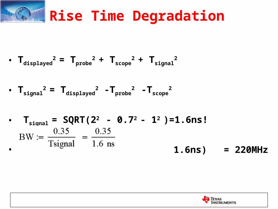
Rise Time Degradation
• Tdisplayed2
= Tprobe2 + Tscope
2 + Tsignal2
• Tsignal2 = Tdisplayed
2 -Tprobe2 -Tscope
2
• Tsignal = SQRT(22 - 0.72 - 12 )=1.6ns!
• 1.6ns) = 220MHz

Critical Microstrip Length
What is the critical length of
a microstrip that must be considered as transmission line?

Rise Time vs. Propagation Delay
0
0.5
1
1.5
2
2.5
3
3.5
0 0.5 1 1.5 2
Rise Time (100%)
Vo
lta
ge
(V
)
Propagation time is 15% of Tr

Propagation Delay vs. Dielectric Constant
050
100150200250
0 1 2 3 4 5 6 7 8 9
Dielectric constant
Tp
d (
ps/
inch
)

Critical Microstrip Length
• Tr x 15% = 1.6ns x 15% = 226 ps
• = 1.5 inch

Transmission Line Model
Zo = V (Z)
I (Z) = sqrt (
L
C )

Characteristic Impedance of Twisted Pair Cable & Microstrip

Reflection Factor
If Z L >> Zo; Г = +1
If Z L << Zo; Г = -1
Zo
Z L
= ZL - Zo
ZL + Zo
Г

S Parameters for Reflection
S11=b1
a1
S21=b2
a1
S22=b2
a2
S12=b1
a2

Reflection Analysis

Reflection Calculation
Load reflection factor
= 1 G - 100
1 G + 100= 1
Source reflection factor
= 20-100
20+100
= -0.8

Calculated vs. Measured Reflection
• Tr/7

Critical Length of a Transmission Line
What is the critical length of
a transmission line that must be terminated?

Rise Time vs. Propagation Delay
0
0.5
1
1.5
2
2.5
3
3.5
0 0.5 1 1.5 2
Rise Time (100%)
Vo
lta
ge
(V
)
Propagation time is 50% of Tr

Trace & Cable Terminations
• Source Termination
Rt + Rs = Zo
ReceiverRt
Zo = 50 Driver
Rs

Trace & Cable Terminations
• AC termination
AC Termination

Place of Terminations
Clock SourceClock Bus
Termination Resistor
Device 1 Device 2
Stub
Daisy Chain Routing with Stubs
Device PinBGA Ball

Short stubs create signal integrity problems
Stub Length=0.5”
Stub Length=0.25”
Reference: Altera
application note 224

Daisy Chain Routing without Stubs
Clock SourceClock Bus
Termination Resistor
Device PinBGA Ball
Device 1 Device 2

Star Routing
Clock Source
Termination Resistor
Device 1
Device 2
Clock Bus
Device PinBGA Ball
Device 3

Parallel Fly-By Termination
Receiver Device
(BGA Package)
R2
Zo = 50
Vcc
R1

Differential Pair (LVDS) Fly-By Termination
Receiver Device
(BGA Package)
100
Zo=50
Zo=50

Crosstalk Analysis
• Cross Talk occurs on PCB and twisted wire cable

Magnetic & Electric Fields of Parallel Transmission Line
VictimTrace
Aggressor Trace
Ground Plane
Magnetic Field
Aggressor Trace
VictimTrace
Electric Field
Ground Plane

Cross Talk Analysis

Cross Talk Analysis

FEXT Measurement
Inductive or
Capacitive Coupling
?

Reduced FEXT Measurement

NEXT Measurement

Reduced NEXT Measurement

Separated Data Wire

Cross Talk Reduced by Termination
X-
talk

Final Termination Solution
+ +
U3 BUF634
+ +
U1 BUF634
+ + U2 BUF634+ +
U4 BUF634
++
U5 BUF634
++U6 BUF634
R1 100
R2 100
R3 100
R4 100
R5 100
R6 100
C1 220p
C2 220p
C3 220p
ADS 8326
CLOCK
CS
CS
MSP 430
DATA
3 feet (1 meter) twisted pair cable
3 feet (1 meter) twisted pair cable
3 feet (1 meter) twisted pair cable
CLOCK
DATA

Conclusions
• The highest frequency signal is determined by switching time
• Transmission line model must be used when propagation delay time is greater than 15% of Tr
• Termination technique dramatically reduces reflection and crosstalk
Q&A

Acknowledgement
Thanks Phil Lizzi for providing the “real life” transmission line application example
Reference:
1. “Managing Signal Quality” Mentor Graphics/Xilinx, 2005 http://www.xilinx.com/publications/xcellonline/xcell_53/xc_pdf/xc_mentor53.pdf
2. “High-Speed Board Layout Guideline” Altera application note 224, Sept. 2003