light nrl-mr-4726 leeeeeeeeeeennnnm mgiighgggegnle …
TRANSCRIPT

A AD110 487 NAVAL RESEARCH LAB WASHINGTON DC F/G 20/7PRODUCTION OF INTENSE LIGHT ION BEAMS FROM A SUPERPOWER BENERAT-ETC(U)JAN 82 F C YOUNG, G COOPERSTEIN
UNCLASSIFIED NRL-MR-4726 NL
LEEEEEEEEEEEnnnnmmgiighgggEgnlEEEEEE.EggggEEI-EE~h~hhEThh
liiil __II 2
111111.2 1. 4 A 112
STMICROCOPY RESOLUTION TEST CHART
NATIONAL Ltd AT O ANDARl 1 A

SECURITY CLASIICATION OF T.I PAGE e7,o, Dot. Enl-'d) A j,. ff~(/-KREAD INSTRUCTIONSREPORT DOCUMENTATION PAGE BEFORE COMPLETING FORM
REPORT NUMBER SS 3 RECIPIEN'S CATALOG NUMBER
NRL Memorandum Report 4726 I Drl4 TITLE (&nd S.btiGz) S TYPE OF REPORT & PERIOD COVERED
PRODUCTION OF INTENSE LIGHT ION BEAMS FROM A interim report on a continuing NRLSUPERPOWER GENERATOR problem.
6. PERFORMING ORG. REPORT NUMMER
7. AUTHOR(.) 11, COPITRIACT OR GRANT UM.."(41)
F.C. Young, G. Cooperstein, S.A. Goldstein*, D. Mosher,S.J. Stephanakis, W.F. Oliphant, J.R. Boiler, J. Maenchenj,R.D. Genuario§, and R.N. Stringfieldt
9. PERFORMING ORGANIZATION NAME AND ADDRESS S0. PRORMEEET RJCTS
Naval Research LaboratoryWashington, DC 20375 47-0815-01
11. CONTRO0LLING OFFICE NAME AND ADDRESS 12. REPORT DATE
Defense Nuclear Agency January 15, 1982Washington, DC 20305 13. NUMBER OF PAGES
5614. MONITORING AGENCY NAME A ADDRESS(II1 ditlO~ro.t from, Coe.Irofini Office) IS. SECURITY CLASS. (.f this report)
UNCLASSIFIEDIS. DECL ASSI FICATION/OWBNGRAING
SCHEDULE
16l. DISTRIBUTION STATEMENT (of this Repot)
Approved for public release; distribution unlimited.
17. DISTRIBUTION STATEMENT (of Ihe *b.1-f t ... td in Block 20. It different Inm, Report)
I0. SUPPLEMENTARY NOTES
*Present address: JAYCOR, Inc., Alexandria, VA 22304.IPresent address: Cornell University, Ithaca, NY 14850.§Present address: Pulse Sciences, Inc., Oakland, CA 94612.tPresent address: Physics International Co., San Leandro, CA 94577. (Continues)
19. KEY WORDS tC-nI... ont -o.-. Odo Of -lCOO.*WyI And Identify by block number)
Pulse power generatorsIntense ion beamsPinch-reflex diodeIon beam focusingHolographic interferometry
20 ABSTRACT (Continuee ont reverse side It necoeeoy And identify by block num~ber)
The operation of a pinch-reflex diode as an intense pulsed ion-beam source has been scaled up toe,, the mult'it2rawatt PITHON generator. Ion beams with currents of 1 MA at 1.8 MeV have been extracted
in a 130 kJ, 100-ns (FWHM) pulse. The corresponding ion production efficiency is 60%. Power losseswere observed in interfacing the coaxial diode to the biconic vacuum feed of the generator. By using 4smaller ares diodes, the average current density at the anode source has been increased to 20 kA/ ;Proton and deuteron beams were studied in both planar and spherical diode geometries. The focusing ofion beams is predominately by self-magnetic fields for planar diodes and predominately by electrode
(Continues)
DD I JA"7 1473 EDITION OF I NOV 65 IS OBSOLETES/N 0102-014-6601
SECURITY CLASSIFICATION OF THIS PACE (%on DON& Enter")
ECURIT'Y CLASSIFICATION OF THIS PAGE. (Wle., Vote Enlo'.d)
18. Supplementary Notes (Continued)
This research was sponsored by the Defense Nuclear Agency under DNA001 -79-C-0023 and under DNASubtask T99QAXLA014, work unit 46, and work unit title "Ion Beam Generation."
20. Abstract (Continued) -
;-shaping for spherical diodes. Current densities of at least 150 kA/9"ewere achieved with spherical diodes.The spatial evolution of the anode and cathode plasmas was studied by laser interferometric holography.As the peak of the power pulse is approached, plasmas were observed to expand from the electrodes infairly uniform profiles with steep density gradients and to accelerate across the vacuum gap. After peakpower, anode plasma fluctuations and a high velocity (30 cm/Ms) axial plume develop; the latter expandsradially coincideit with collapse of the power pulse..
4
SECURITY CLASSIFICATION OF THIS PAGOE(UYla Det Enered)
ii

CONTENTS
I. INTRODUCTION ......................................... 1
II. EXPERIMENTAL APPARATUS.................................2
III. DIAGNOSTICS .............................................. 9
IV. EXPERIMENTAL RESULTS ................................. 20
V. SUMMARY OF RESULTS ................................... 41
REFERENCES ........................................... 44
I Accesio For
Jt
Distributionl/DTICE E TEf Avilabi~itY Cods
Av1 and/orFEB 3 1982 jD15t SP-cial
B
ift
---- DTC B

PREFACE
The purpose of the research effort described in this report was to
investigate the scaling of the pinch-reflex ion diode, developed at the Naval
Research Laboratory (NRL) on the Gamble II generator under Defense Nuclear
Agency (DNA) auspices, to the higher power and longer pulse length of the
PITHON generator at Physics International Co. (PI). A collaborative effort
between NRL and Pl was carried out with DNA support under contract DNA 001-79-
C-0023 at PI and contract DNA Subtask TAQAXLAO14 at NRL. The DNA contract
officers were J. Z. Farber and R. L. Gullickson.
Experimental measurements on the PITHON generator were carried out in two
4-week sessions during Aug.-Sept. 1979 and April-May 1980. A total of 46
shots were fired in the first session and 41 shots in the second session.
Analysis of the data accumulated from these shots has continued up to the
present time.
The extensive set up of diagnostics on the experiment and the detailed
data analysis has involved the support of the following personnel. Lead
technician H. J. Kishi at PI designed and directed hardware construction and
assembled the diode hardware on each shot in the first pulsing session.
During the second session T. Robinson of NRL was responsible for the diode
assembly. B. Hartneck of PI supported operation of the laser holographic
system. The transfer of data to NRL and the development of software routines
for data analysis was carried out by D. Bacon and D. Hinshelwood of NRL,
Finally, the support and encouragement of PI management including
A. J. Toepfer, S. Putnum and K. Childers in carrying out this collaborative
effort is gratefully acknowledged.
iv
..... • ... .. ... . -. . . . '-, ... . - . . ... . , - . .. ..
PRODUCTION OF INTENSE LIGHT ION BEAMSFROM A SUPERPOWER GENERATOR
I. INTRODUCTION
Recent technological advances in the production and focusing of intense
pulsed light ion beams (hydrogen, deuterium, and carbon) have raised the
attainable intensities from levels of 1 A/cm 2 into the MA/cm 2 regime. I-3 The
present achievements of high-power ion beams and the potential for continued
advancements in thi" field make them prime candidates as drivers for inertial
confinement fusion (ICF). Requirements of an ICF system that are met by an
ion beam driver 4 -6 include: (1) ions can be produced at high efficiency in
extraction geometries appropriate to ICF ignition, 7 "9 and (2) beam power
density delivered on target can be significantly larger than the source
density through velocity bunching of the ions during transport,10 by
geometrical shaping of the ion source, 8 or by externally magnetically focusing
the extracted ion beam.7 A specific advantage of an ion beam driver for ICF
is that the ion energy deposition profile in the target is more favorable than
those of either laser photons or relativistic electrons 11 .
A variety of diode configurations to produce light ion beams for ICF have
been discussed in the literature.1 In this paper, experimental investigations
into the production and ballistic focusing of proton and deuteron beams from
one such diode are presented. The pinch.,reflex diode, 8 developed by the Naval
Research Laboratory (NRL) on the Gamnble II accelerator, was matched to the
PITHON generator 12 at Physics International Company. In addition to diode
physics studies, the coupling between a biconic magnetically insulated vacuum
transmission line and a small pinch-reflex diode at high stress (E > 2 x 10⁶
V/cm) has been investigated.
The early motivation for this work stemmed from computational modeling of
the pinch-reflex diode toward ICF applications. The PITHON generator
parameters may satisfy requirements for a single module in a multi-ion-beam
target irradiation concept based on beam bunching during transport in Z-
pinches 13 and multi-beam overlap on target. Two experimental sessions were
performed with this generator: The first studied the scaling of diode
performance and ballistic focusing at higher powers and longer pulselengths
than previously available;2 the second studied the detailed shape evolution of
the electrode plasma surfaces--information essential for design of a diode to
produce a high quality focused ion beam. 14
Manuscript submitted November 10, 1981.

In this paper we present the results of these studies. The generator and
diode are discussed in Sec. I. The beam diagnostics employed to evaluate ion
species, current density profile and history, time-integrated beam geometry,
and anode plasma surface evolution are described in Sec. III. The principal
results of the two experimental sessions are presented and discussed in
Sec. IV. Conclusions of this work are presented in Sec. V.
II. EXPERIMENTAL APPARATUS
A. Accelerator
The PITHON accelerator, shown schematically in Fig. I, is a water
dielectric multi-stage coaxial transmission line driven by a 40-stage, 1.5-MJ,
oil-insulated, twin Marx generator. The 2.3 i intermediate storage capacitor
is charged to a voltage above the open circuit Marx potential (through
ringup), then discharged via a single-site, self-breaking water switch into a
1.3-a pulse forming line (PFL). Multi-site water output switches provide a
low-inductance energy transfer from the PFL to a tapered 1.0 s first
transformer in a pulse of about half the PFL voltage and twice the duration.
A comon problem in pulsed power accelerators is a low-voltage, long-
duration "prepulse" loading, the diode prior to the main high voltage pulse.
This phenomenon is due to capacitive coupling between sequential inner
conductor stages of the accelerator and can often lead to diode shorting and
nonreproducibility. This coupling is reduced in PITHON by a low permittivity
epoxy "prepulse slab" between the first and second transformers (see Fig. 1).
For a shot yielding a 2-MV output pulse, this technique reduces the prepulse
level at the vacuum interface from over 300 kV to below 10 kV thus allowing
the use of a wide variety of field-emission-diode loads.
Multi-site, gas-insulated switches connecting the transformers through
the prepulse slab close on the leading edge of the high voltage pulse. There
are two interchangeable second transformers which connect this slab to the
water-vacuum interface with characteristic impedances of 0.75 and 1.0 a. Both
interfaces allow penetration of a "transit time isolator" cable shield through
the water from the high-voltage vacuum cathode to the grounded outer shell.
Through this isolator the ion-beam diagnostic signals, floating at the 2- to
2.5-MV cathode potential, can be extracted with less than 50-mV noise.
2

L4L
Lcn
w
20 cc >
zo o ,,
U ca
U- 0Z 0ULl
4 C , (A
4 D u
-wV) z 4
I-D T
z
w
3L
CC-.- * CC CC j4
The vacuum feed connecting the second transformer to the diode is shown
in Fig. 2. The shaded area is the water-dielectric transmission line, which
carries the electromagnetic wave. The line bends radially inward and flares
to reduce the electric field stress on a graded axially-stacked epoxy
interface separating water from vacuum. Interface voltage and current
diagnostics (VT and IT) are located at the flare in several azimuthal
locations. On the vacuum side of this interface, the energy pulse is carried
by an electromagnetic wave and by electrons. The total current can be
measured on the anode and is monitored at the vacuum interface (1o) and at the
diode (ID). The total inductance between these monitors is about 30 nH. A
dielectric surface flashover switch interrupts the cathode side of the feed to
further reduce the prepulse on the diode to about 5 kV.
B. Diode Structures
Two independent cathode and anode configurations were tested in these
experiments. The diode structures used in the first run are shown in Fig. 3.
Following the vacuum feed from the flashover switch toward the axis, a sudden
transition is made from a radial biconic to a coaxial feed. The center
conductor is the cathode shank, a 0.6-cm-thick wall stainless-steel
cylinder. The outer coax anode shell is aluminum and can be adjusted for
concentricity and axial spacing. This coax section terminates in the pinch-
reflex diode: a thin hollow cathode tip opposite a grounded planar or
spherical anode.
A planar pinch-reflex diode is shown in Fig. 3a. The anode assembly is a
disk of 0.012-cm-thick polyethylene (CH2) held 5 mm from a carbon backing
plate by an outer insulating annulus and a central carbon button. When this
foil flashes early in the electrical pulse, an anode plasma spreads across the
foil and expands into the anode-cathode gap. Ions are accelerated toward the
cathode from the low-density front of this moving plasma and are deflected
radially inward by their self-magnetic field toward a time-varying collection
of foci. The ion beam current (lion) is measured by a Rogowski coil sheltered
behind the cathode tip. The ions entering the cathode pass through a 1.8-pm-
thick polycarbonate (Kimfol*) foil pressure window and propagate current- and
charge-neutralized in a l-Torr-nitrogen drift chamber.
*available from Kimberly Clark Corp., Lee, MA, 01238
4
-4 ~ 77

FINALTRANSFORMER
WATER-VACUUMINTERFACE
RADIAL BICONICVACUUM FEED
I VACUUM,,W'CHAMBER
TRANSIT TIME CAISOLATOR
SURFACE FLASHOVERPREPULSE SWITCH
Io
Fig. 2 - Schematic of the vacuum feed interface on PITHON5. ......
. . . . . . . . .. .

DIELECTRIC BICONIC VACUUM FEED(a) ~ FLASHOVER\,(a) SWITCH
6.4 mm 6061 Al CAHDLI
WITNESS PLATE~~-AR ON ANODE
BACKING PLATE
PLASTIC ANODE
-~--KIMFOL PRESSUREWINDOW
1-or N2 GAS-
GASBA 11ONFILLED DRIFT
(b)
0 ~ -~-SPHERICAL ANODE
INET BACKING PLATE
250 pmn PVA FOIL
Fig. 3 - Pinch-reflex diode assemblies for the first experimentalsession in (a) planar geometry and (b) focusing geometry
6
C - - ---- ---- 2

The focusing configuration of the pinch-reflex diode in the first
experimental session is shown in Fig. 3b. Anode foils of 0.025-cm-thick poly-
vinyl-acetate (PVA), deformed into a spherical section with a 12.7-cm radius-
of-curvature, were mounted onto similarly machined carbon backing plates to
maintain a 5-mm foil-plate separation (see Fig. 3b). An extended tip cathode
was used to define the 100-cm 2 diode area for pinch-reflex electron operation
with a 3- to 4-mm anode-cathode gap. The initial ion velocity is directed
toward a geometric focus located substantially inside the planar-diode focal
length. The intent of this design is to create a high-current-density ion-
beam focus which is less sensitive to self-deflection variaions during the
pulse 14 and from shot to shot.
The diode structures used in the second session were somewhat different
from those shown in Fig. 3 and are displayed in Fig. 4. The coax gap was
increased to form a higher inductance but constant characteristic impedance
5-u transition from the biconic into the coaxial feed. This design represents
an attempt to improve the vacuum power flow into the diode structure. The
thick stainless-steel cathode shank was severely distorted after a few PITHON
shots in the first run and has been replaced with disposable spun aluminum
cylinders in this design. By sealing the inner cathode volume with Kimfol
glued to the tip of the ion Rogowski assembly, the inside of the cathode is
pressurized to l-Torr nitrogen while the surrounding volume is at ambient l0-5
Torr pressure. Variation of cathode radius was engineered by spinning a
smooth taper on the cathode tip. Figure 4a shows a 100-cm 2 cathode bore,
while Fig. 4b shows a smaller 30-cm 2 area diode.
The coax length was extended to allow access for direct viewing across
the diode gap with a ruby laser holographic system. Planar diodes were used
and disposable anode backing plates were fabricated of spun aluminum in which
an array of viewing slots were machined. The slots were made as symmetric as
possible consistent with direct viewing to avoid return current asymmetries.
Finally, a 7.6-cm-diam central carbon insert was pressed into the backing
plate to minimize bremsstrahlung and to reduce aluminum buildup on the
reusable diode hardware.
7 4

FLASHOVERSWJ C H
LASER ACCESSDO ANODE BACKING PLATE
TRANSMISSIONl__, I, U FOIL
1 TORR N2 DRIFT REGION ISR
/i~ f ANODE-. ___-F O IL
ION
(b)
,i L L-[
Fig. 4 - Pinch-reflex diode assemblies for the second experimental sessionfor (a) a 100-cm 2 area diode and for (b) a 30-cm 2 area diode
8
I1. DIAGNOSTICS
In this section the generator, beam, and plasma diagnostics will be
described and data reduction procedures will be discussed. These include:
generator voltage and current detectors distributed in the vacuum feed;
bremsstrahlung diagnostics for the electron-beam pinch history and time-
integrated x-ray profile; a Rogowski coil to measure the ion-beam current; a"shadow box" diagnostic for spatial-profiling of the ion beam; nuclear-
reaction diagnostics for ion-beam duration and fluence; and interferometric
laser holography for evolution of the anode and cathode plasmas.
A. Electrical Measurements
The accelerator diagnostics for voltage and various currents are shown in
Fig. 2. The injected voltage is measured by balanced capacitive dividers (VT)
at several azimuthal locations in the water, displayed separately to evaluate
wave symmetry, and averaged to calculate impedance, power and energy. The
injected current is monitored both in the water adjacent to the voltage probes
(IT) and in the vacuum (Io) at the entrance to the radial biconic transmission
line with dB/dt and segmented Rogowski probes, respectively. The difference
between these measurements affords insight into water or vacuum arcs in the
interface and transition regions. The total diode current (1o) is measured
with a self-integrating Rogowski coil15 as is the ion current (see Figs. 3 and
4). These current monitors have risetimes of less than 5 ns and integration
times greater than 3.4 ps . Several designs are employed to shield the epoxy
encapsulated coils from particle bombardment and UV irradiation while
minimizing the monitor inductance. On most shots, valid ion current
measurements are obtained from power onset to peak. All current monitors are
bench tested and cross-calibrated in short circuit shots. The data are
monitored through a 200-MHz bandwidth 7912R transient digitizer system
controlled by a PDP 11/40 computer and are reduced numerically.
B. X Rays
The ion power and energy on each shot are qualitatively correlated with
the yield of bremsstrahlung radiation and the symmetry and size of the
electron pinch as evidenced by its x-ray image. Because the bremsstrahlung
yield scales with diode potential, a large x-ray signal with a large FWHM (40-
60 ns) indicates a high-voltage, long-impedance-lifetime shot.
9
I I I I I-

The time-resolved x-ray output from the electron pinch is monitored with
an optical photodiode (PDX) coupled to a plastic scintillator. The unit is
rigidly mounted outside the vacuum chamber at 1800 to the diode axis.
Similarly mounted is an x-ray pinhole camera to record hard photons (E > 30
keV) from the diode region through a 0.05-cm-diam 200 tapered pinhole. This
camera images the diode onto a stack of Kodak No-Screen, XR5, and Polaroid
Type 52 films coupled to a variety of intensifier screens. This wide range of
film sensitivities to x rays affords good contrast over the variation of
bremsstrahlung intensity across the diode image. Lithium fluoride
thermoluminescent detector (TLD) capsules monitor the time-integrated
bremsstrahlung dose at the photodiode fron the entire anode. Serious current
losses in the vacuum feed were correlated with the photographic, TLO, and PDX
data as well as with visual damage following a shot.
C. Ion Imaging
The location of the ion-beam focus was determined by using ballistic
reconstruction of ion trajectories from the edges of ion-induced melt damage
patterns recorded on the rear witness plate of a shadowbox (see Fig. 5). The
interpretation of this data is based on several key assumptions. These are:
the ions are accelerated from a planar anode plasma with initial velocity
vectors ;arallel to the axis; as they cross the anode-cathode gap each ion is
magnetically deflected by the field of a calculated ion-current-density
profile. 16 Upon crossing the cathode foil and entering the 1-Torr-nitrogen
drift chamber, the ions are assumed to be charge and current neutralized and
hence execute straight-line orbits through a focal region and expand into the
shadowbox. The current neutrality premise has been verified by measurementsof the net-current fraction in the gas (1net/lion) of less than 2% on both
Gamble I (Ref. 2) and PITHON. The damage patterns on the witness plate of
the shadowbox are projections of the ion beam through the front apertures (see
Fig. 5). The patterns, which are time-integrated records, often form teardrop
or oval shapes. The radial variation is attributed to the change in focal
length during the pulse due to time-varying diode fields. The azimuthal width
of the damage is due to the divergence of the ion beam from the anode plasma,
asymmetries in the source, and scattering through the transmission foil. The
computer reconstruction, shown in Fig. 5, traces the recorded damage areas
back through the front-plate apertures, through the focus, and onto the anode
10
. . -

WITNSS PATE ESTOCUSANHODE
AIIOSAND0 0
HOF I
00CU
Z 35 c 20 cm 0c
Fig. 5 -Shadowbox geometry and reconstruction of ion-beamtrajectories for planar-diode Shot 1676

surface. The large damage patterns at the smallest radii on the witness plate
are due to the time-varying focal spot moving through the shadowbox location
and are not useful in planar geometry reconstructions.
D. Nuclear Diagnostics
The intensity and duration of proton or deuteron currents were also
monitored by nuclear-reaction techniques. For proton beams, a prompt
y-ray diagnostic 1 7 was employed utilizing the 19F(p,ay)160 reaction. Teflon
(CF2) targets were placed in the ion-beam path, and 6-MeV prompt y rays were
measured with a fast scintillator (NE-111) and photomultiplier (XP-2020)
detector housed in a 3.2-cm-thick lead enclosure located 4 m from the ion
diode at 950 to the diode axis behind a one meter-thick concrete shielding
wall. This wall differentially shields the diode bremsstrahlung and improves
the y-ray-to-bremsstrahlung ratio. Measured and calculated signals for this
detector on a shot with a CH2 anode and Teflon target are compared in Fig. 6.
This detector could not be calibrated absolutely as the attenuation of the
prompt-y signal by the concrete shielding wall is difficult to estimate.
The total yield of deuteron beams was determined by measuring neutrons
from the D(d,n) 3He and 12C(dn)13N reactions. Deuteron beams, produced by
using CD2 coated PVA foil anodes, were directed onto thick CD2 targets to
produce these reactions. Because the ion beam was directed into the generator
in these experiments, neutron measurements were confined to recoil angles
greater than 900. Total neutron yields were measured with two rhodium
activation detectors 18 located 17 m from the diode at 1750 to the diode
axis. These detectors viewed the diode through a 30-cm-diam hole in a
concrete shielding wall located 8.3 m from the diode. This geometry minimized
the number of room-scattered neutrons which reached the detectors and allowed
the intensity of the direct collimated neutron beam to be scaled inversely
with the square of the source-to-detector distance, even at 17 m. These
rhodium activation detectors were calibrated with a 25 2Cf neutron source as
described in Ref. 18. Deuteron intensities were inferred from measured
neutron intensities hy using D(d,n) 3He and 12C(d,n) 13N reaction yields.
Thick-target yields for these reactions were calculated from measured cross
sections1 9 ,20 and published stopping powers21 and are presented in
Fig. 7. Above I MeV, the 12C(d,n) 13N reaction contributes significantly to
the neutron yield.
12

3
2
Uio 0D 0
0.
I-0 0
0
00
100 200 300TIME, ns
Fig. 6 - Prompt--y signals measured on Shot 1665 (solid line) and calculated (opencircles) for protons on a thick CF 2 target. The calculated trace has been normalizedin amplitude to the measured signal. Good agreement in pulse width and shape isshown.
13
I "

8
Thick Target YieldsCD 2 Target
0,, 1750
6
z0 D(d,nP'He ± C(~)N
w
C 4
cc(a
0
D (dn)H He
2
12 3
DEUTERON ENERGY, MeV
Fig. 7 - Thick-target yields for the D(d,n)3 He and12 C(d,n) 1 3 N reactions at 1750
14

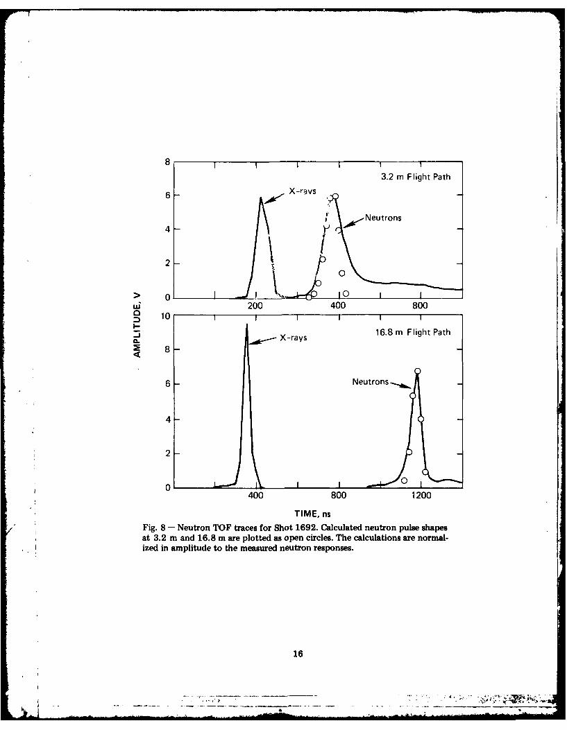
The neutron time-of-flight (TOF) technique was used with the D(d,n) 3He
reaction to determine neutron energies and to monitor the duration of the
deuteron beam. Neutron energies were determined with a TOF detector located
16.8 m from the diode in the same geometry as the rhodium activation
detectors. This detector consisted of a fast scintillator (NE-111) quenched
with 5% piperidine 22 and photomultiplier (XP-2020) mounted within a 7.6-cm-
thick lead shield. To operate this detector in the linear range, the light
incident on the photomultiplier was attenuated with an ND-1 filter. The time
history of the deuteron beam was determined using a TOF detector with a
relatively short flight path as described in Ref. 23. For this purpose, a
detector was located 3.2 m from the diode at 1600 to the diode axis. This
detector consisted of a similar fast quenched scintillator (NE-111), an ND-2
filter, and a photomultiplier (XP-2020) mounted within a 10-cm-thick lead
shield. Typical traces from these two TOF detectors are shown in Fig. 8 along
with calculated neutron pulse shapes for these detector locations. For the
detector at 16.8 m, the time interval from the peak of the bremsstrahlung to
the peak of the neutron signal was used to determine the neutron energy. An
energy of 1.9 ± 0.2 MeV, consistent with the diode voltage, was determined
from this trace after correcting for the x-ray flight time. For the detector
at 3.2 m, the duration of the neutron signal gives a measure of the duration
of the deuteron beam. The width (FWHM) of this neutron pulse is 60 ns, which
compares favorably with the duration of the ion pulse based on the measured
diode voltage and ion-current traces for this shot.
E. Interferometric Holography
The final diagnostic to be described is the interferometric holography
system 24 used to monitor the anode and cathode plasma motions in the
interelectrode gap. The system configuration is schematically illustrated in
Fig. 9. The system employs a 6-ns ruby laser pulse, which is split into four
beams. These are delayed by path length into lO-ns increments to form a train
of four laser pulses over a 30-ns interval. Each of these four beams is split
into a scene and reference beam. Each scene beam passes through the pinch-
reflex diode and then through lenses and mirrors to form a real image of the
diode on a glass holographic film plate. The reference beams are directed to
the film without passing through the diode, overlapping their respective scene
beams to produce an array of four holograms on the film plane. Two such sets
15
- - - - -- - - - - - - - - - - - - - - - - - - - -... - ------ -i ____
83.2 m Flight Path
X-ravs
I f Neutrons4 t
20
> 0 10 1
200 400 80010 I 1 1
I-X-rays 16.8 m Flight Path
8
6 Neutrons
4
2
001
400 800 1200
TIME, nsFig. 8 - Neutron TOF traces for Shot 1692. Calculated neutron pulse shapesat 3.2 m and 16.8 m are plotted as open circles. The calculations are normal-ized in amplitude to the measured neutron responses.
16
• - "-' ," , .'," 1"%A.; .

Laser PITHON
aFour Beams
Beam Lne
Sp itters 4) -~Diode L ne
Reference Beams (4)--
IBeam Espanding
Scene Beams (4)
1 ur1n) Plane
Fig. 9 -Ion-diode laser interferometric holography system
17

of holograms are superposed: one made before the shot and the other during
the shot. The two sets of interference patterns overlap to form four Moire
patterns. The differences between a superposed pair of holograms are due to
optical-path-length variations in the scene beam where it passes through the
diode plasma.
3y shining light through a developed interferometric hologram, both an
image of the diode and series of fringes can be seen. As an aid to data
interpretation, a uniformly changing optical-path-length difference between
the two hologram sets is introduced by slightly tilting one of the mirrors ,n
the system after the first set is exposed. This produces a reference array of
uniformly spaced straight fringes on the image where no plasma is present.
Additional changes in the optical path length caused by plasma result in
bending of the fringes: the bending of a fringe over the distance of one
reference fringe spacing corresponds to an additional wave length of path
difference due to the plasma. The corresponding plasma density can be
estimated by the relation:
ne AX = 3.2 x 10¹⁷/cm2/fringe shift
where AX is the total path length through a uniform plasma of density ne. The
largest plasma line density measurable by this technique is that for which the
index of refraction equals zero (i.e. ?.3 x 102 1/cm2). The maximum density
observable in this experiment is estimated to be between 1019 and 1020 due to
ray-tracing effects: large-angle refraction of the laser beam by higher-
density plasmas reduces the light intensity entering the optical system and
the exposure level on the film.
Unfolding the detailed radial-density profile is not possible with this
technique. Figure 10a shows the diode area with the laser-viewing slots
machined out of the anode: the shaded area is the laser-beam cross section,
and the clear holes are the observable diode regions. It is important to note
that the view through a hole pair is a chord across a disk system which may
not be axially symmetric: a thin plasma ripple in an orientation other than
the laser axis will appear to be a large-area plasma motion. Further, anode
plasma which crosses the visual anode-cathode gap inside the cathode inner
radius does not necessarily contact the cathode plasma lifting off the hollow
18
* -Li. - "

D LASER'IONB AMS
(a)
LASERLPHOT
Fig. 10 - (a) Ion-diode laser diagnostic detail, and(b) reconstructed holographic interferogram
19

emission ring. Despite these limitations, the system presents new information
about the plasma surface evolution which is important for the design of high-
focus-quality diodes.25
IV. EXPERIMENTAL RESULTS
A variety of experimental goals were addressed in the two pulsing
sessions. The first session extended scaling of the pinch-reflex ion diode to
the higher power and longer pulselength of the PITHON generator. Both planar
and spherical anode foils were tested. The second session utilized modified
accelerator impedance and vacuum feed hardware. Emphasis was placed on
determining the electrode plasma evolution in the diode, the scaling of diode
parameters with cathode radius, and the consequences of diode modifications.
A. Planar Diode Experiments
The important scaling parameters studied in these experiments were the
ion efficiency, the ion turn-on time, and the diode-impedance lifetime. The
PITHON generator was chosen for these scaling studies for its similarity to
Gamble II in minimal prepulse, similar impedance (1.0 versus 1.5 1) and
voltage risetime, yet larger peak voltage and pulsewidth. These similarities
suggested the physics of the pinch-reflex diode would be the same and detailed
comparisons could be made between equivalent power PITHON and Gamble II
shots. These comparisons, performed during the first session, confirmed the
baseline similarity between the accelerators. The scaling variables are then
the 70% larger and 30% longer FWHM power pulses available on PITHON.
Theoretical calculations 8 based on the generator open-circuit-voltage
waveforms predicted a doubling of the Gamble II ion currents to about 1.0 MA
of protons from a pinch-reflex diode on PITHON.
A typical waveform data set from the first experimental session (Shot
1662) is shown in Fig. 11. The injected voltage and current measured at the
water-vacuum interface (see Fig. 2) have 2.1-MV (VT) and 2.0-MA (1o) peak
values at a mean impedance of 1.2 az. These signals indicate a 4-TW power
pulse of 88-ns FWHM containing 340 kJ is injected into the vacuum feed
structure. The voltage impressed on the diode (VD) is less than the injected
voltage by the L(dI/dt) inductive drop due to the wave passing through the
20

Cx
0~0
0w
L:) 0000
Zu 'U
ww0 0o
0.0800
zL z
-43
0
U
z 0z
0 0l 0 0_r L, z
m
-r
C121

vacuum feed. The effective inductance is determined to be 30 nH by defining
the potential across a shorted diode to be zero. There is a current loss in
the vacuum feed shown by the difference between the interface (1o) and diode
D) current waveforms. The total electron current in the system (E) isdefined as the difference between the interface (Io) and ion (lion)
currents. Despite the losses in the vacuum feed, 2.7 TW and 230 kJ were
coupled into the diode on this shot. The ion-beam current entering the 100-
cm2 cathode bore (0.9 MA at 1.7 MV) begins 22 to 26 ns after the diode
current, a delay characteristic in all these experiments. The resulting peak
ion power and energy are 1.6 TW and 125 kJ respectively. These data
correspond to an average source current density of 12 kA/cin2 , which is in
agreement with numerical predictions.
The diode-impedance lifetime is an important consideration in scaling the
ion diode toward an eventual ICF application. The velocity bunching desired
for power multiplication requires carefully programmed voltage and impedance
histories. The diode impedance shown in Fig. 11 reaches a plateau near 1.1 1
for 40 ns then slowly falls until the end of the applied pulse. Accurate
impedance control was provided by anode-cathode gap adjustment, with shot-to-
shot variations of 0.2 1 obtained throughout the experimental sessions.
The ion Rogowski coil located inside the cathode provided timing of the
formation of an anode plasma on the cathode side of the anode foil.
Frequently a low-level signal is seen starting with the diode current (see
Fig. 12), due perhaps to a small anode-foil hot spot or to electrons emitted
from the ion Rogowski holder and transmission foil. Several explanations for
the 22 to 26-ns delay for ion turn-on are possible. One conjecture, based on
pinched-electron-beam-diode physics 26 is that before the anode foil flashes,
forming a plasma and bringing the floating dielectric foil to ground
potential, the electron beam passes through the anode foil and pinches on the
backing plate. Previous pinched-electron-beam experiments 27 on PITHON have
measured pinch areal velocities of 5 cm2/ns, or a value of 20 ns for the
present 100-cm 2 experiments, which is consistent with the measured delay. The
resulting high field stress on the foil adjacent to the central button could
then cause surface flashover. If this mechanism is responsible for anode-
plasma formation, the small-area (30 cm2) diodes tested should exhibit a much
smaller delay in ion turn-on time of roughly 8 ns. These results, presented
22

400
SHOT 1888
300
zW 200IO
100
0 20 40 60
TIME, nsFig. 12 Early-time behavior of the diode- and ion-current traces
23
A - --L

later, show no discernible change in the delay of ion turn-on. An alternative
explanation for the ion delay is that it represents the inherent delay of
surface flashover. For these large and small area diodes, the difference in
delay would be ± 5 ns which is within the shot-to-shot variation.
The radiation diagnostics provide corroboration of the relative timing
and waveshape of the diode voltage, injected current, and ion current. The x-
ray photodiode signal (PDX) for Shot 1662 is shown in Fig. 11 and compared
with a calculated waveform (XE). The theoretical scaling 2 g for x-ray
production from electron beams is given by XE = IE(VD)2 "8 , which is a
sensitive measure of voltage waveshape. The calculated waveform was
normalized in magnitude and shifted in time for the comparison, and the shapes
of the two signals agree reasonably well. This agreement provides an
independent check on how well the measured voltage and electron current pulse
shapes represent the actual wave shapes at the diode. Similarly, the
agreement between the measured and calculated prompt-y nuclear radiation
signals 17, shown in Fig. 6, indicates that the diode voltage and ion current
pulse shapes are correctly timed and are of reasonable proportion.
The ratio of the ion current to the diode current provides a direct
measure of the pinch-reflex-diode efficiency for ion production. At maximum
power the efficiency on Shot 1662 is 60% for an ion current of 900 kA.
Bremsstrahlung measurements, as described in the next paragraph, indicate that
the electron beam formed a well-centered pinch with good coupling of the
injected energy to the diode on this shot.
Bremsstrahlung diagnostics were used to study the symmetry of power flow
and current loss in the vacuum feed and diode regions. Measurements for two
different classes of shots are compared in Fig. 13. A well-centered pinch
with bremsstrahlung from only the central 2 cm of the 12-cm-diam anode is
observed in the x-ray pinhole photograph in Fig. 13a. For this shot, the x-
ray photodiode signal (PDX) is substantial for the entire diode pulse
duration, and the energy at the vacuum interface (ET) shows good coupling of
the injected power to the diode. A second class of shots is shown in Fig. 13b
where the power flow is asymmetric and the electron pinch is not well
centered. The x-ray pinhole image shows flutes extending onto the aluminum
backing plate, and bremsstrahlung from the coax feed at 9-cm radius is seen.
Intense bremsstrahlung emission from aluminum and stainless steel, relative to
24

0 0 0 0 0
0 00C C
C C
C c 0
o ca
o 0 0 0 0 0 0 0) 0- CNJ C1 - V- CV- 1
se'noVoIij AD~~~n anig~ A'9VJLN-10 f
________ 0 0 0
owa
00
x 25

carbon, allows electron losses in the vacuum feed at low current density to
have intensities comparable to the intense central pinch on carbon. On this
shot the PDX trace is smaller in amplitude and narrower in pulsewidth,
indicating a reductio, in diode voltage. Also, a significant fraction of the
injected energy is reflected off the load. Visual damage to the feed hardware
was consistent with the origins of x rays indicated in Fig. 13 on these two
shots.
The shadowbox diagnostic was used to determine the time-averaged location
and size of the focus as indicated previously in Fig. 5. A model developed to
predict the best focus location 14 yielded a minimum spot size at about 18 cm
from the anode foil for the voltage and current values of a typical 3-TW
shot. The ballistic reconstruction shown in Fig. 5 gives a best focus at 20
cm, in good agreement with this prediction. Witness plate targets of 6.4-mm-
thick aluminum (6061-T6) placed at this location showed centered front surface
damage and backspalls about 1 cm in diameter (see Fig. 14).
B. Focusing Diode Experiments
Experiments investigating geometric focusing of high power ion beams from
a pinch-reflex ion diode, which were first performed at NRL on Gamble II (Ref.
8), were extended to higher power in the present experiments on PITHON. It is
important to note that the voltage, current, and impedance characteristics of
the focusing diodes are essentially the same as those of the planar diodes.
The ions are magnetically deflected in passage across the anode-cathode gap,
then drift ballistically in the 1-Torr gas to an actual focus at about 9 cm
from the anode foil, inside the geometric focus located at 12.7 cm. This
magnetic bending is demonstrated by shadowbox reconstructions shown in
Fig. 15. The damage patterns extrapolate back through the focus to cover the
entire anode plane. The focal spot is seen to be within a 3-cm-diam circle,
* corresponding to an areal beam reduction from the anode source of 14. A
preliminary estimate of the focused current density can be made by assuming
the entire measured ion current is uniformly distributed over this disk of
least confusion. The calculation yields an ion current density of 150 kA/cm 2
over the 7-cm 2 spot. Peak focused current densities could be significantly
larger. Witness-plate targets located at the focus exhibit multiple layered
backspalls through plates of 6.4-mm-thick aluminum (6061-T6), consistent with
higher focused current densities than found in the planar-geometry shots.
26

[ l I& 11 1, 1
0 10cmFig. 14 - Witness plate damage on Shot 1663 for a 6.4-mm-thick aluminum(6061-T6) plate located at the approximate proton self-focus of a planarpinch-reflex diode
27

15 cm 12cm 8cm 0CMI I II
ANODE BACKINGPLATE
CALCULATEDORBI'TS -,
GEOMETRIC ACTUALFOCUS FOCUS
250 im PVAANODE FOIL
12.7 cm RADIUS OF
CURVATURE
I ""-CATHODE
TRANSMISSIONJ I \FOIL
SHADOW BOXFOU
ANODE FOIL
v
I *
a 3 \c
Fig. 15 Shadowbox geometry for a focusing pinch-reflex diodeand reconstruction of ion trajectories for Shot 1863
28

C. Results from Neutron Measurements
The energy of neutrons from the D(d,n) 3 He reaction was determined by the
TOF technique. However, this measurement could not be used to determine the
deuteron energy (i.e., diode voltage) because the neutron energy is
insensitive to the deuteron energy for the d-d reaction at the 1750
measurement angle. Furthermore, the focusing of deuterons in the diode
introduces an uncertainty in the neutron emission angle. Neutron energy
determinations are consistent with deuteron energies given by the diode
voltage. The measured ion current and diode voltage were used to calculate
neutron responses as shown in Fig. 8 (Ref. 23). The shapes of the measured
and calculated responses are in good agreement. The low energy tail on the
trace at 3.2 in is attributed to scattered neutrons.
For both the planar and focusing diode experiments the measured neutron
yields are about 1/3 of yields calculated using the measured ion current and
diode voltage corrected for energy loss in the Kimfol. For the planar-diode
geometry, the calculated yields are based on the combined thick-target yields
for the D(d,n) 3He and 12C(d,n) 13N reactions at 1750 as shown in Fig. 7. For
the focusing-diode geometry, a broad range of neutron emission angles (1400-
1800) exists due to the angular spread of the deuterons incident on the CD2
target. In this case the calculated yield is based on thick-target yields at
different angles weighted by an ion-current-density profile 16 determined from
numerical simulations. The difference between the measured and calculated
neutron yields may be attributed to several factors: 1) The measured ion
current may include significant proton or carbon-ion components which
contribute very little to the neutron output; 2) Ion energy losses in the
region from the anode to the CD2 target,30 which have not been taken into
account in the neutron-yield calculation, may reduce the ion energy on target31and hence the neutron yield; and 3) Enhanced deuteron stopping in the hot
dense plasma target may lead to a reduced neutron output, particularly in the
focusing diode geometry. A quantitative assessment of the importance of these
factors in the present experiments is not possible.
The largest neutron yield at 1750 was obtained with the planar-diode
geometry because the d-d neutron yield peaks at 1800. For this diode, neutron
yields of up to 4.5 x 10¹¹/sr were measured. At the diode voltage of 1.7 MeV
corresponding to this yield, approximately 50% of these neutrons are from the
29

D(d,n) reaction (see Fig. 7). The corresponding total neutron yield into
4 n, corrected for the anisotropy of neutron emission, is 3.7 x 10¹² with 50%
from the D(d,n) reaction.
With the focusing-diode geometry, time-integrated neutron yields were
used to determine focused current density by comparing neutron yields from
different area CD2 targets. For this purpose, the measured neutron output was
scaled to the current measured by the ion Rogowski coil. The fraction of
deuterons incident on targets as small as 0.75 cm2 was determined by comparing
the neutron yield with the yield measured on 100-cm2 area targets. On the
0.75 cm2 area target, the neutron yield was still about 50% greater than that
observed without any CD2 target. To correct for variations in neutron output
in these measurements due to shot-to-shot variations in voltage and current,
the measured yields were scaled to yields calculated from the measured diode
voltages and ion currents. A deuteron current density of 150 kA/cm 2 at peak
ion voltage was determined from these measurements. If the ion current is
only 1/3 deuterons, as suggested by comparisons between measured and
calculated neutron yields, then the total ion current density may be 2 to 3
times larger than this value.
D. Power Flow Studies
Problems in power flow from the PITHON accelerator to the pinch-reflex
ion diode occurred in the magnetically insulated vacuum transmission line
where a vacuum flow of electrons crossed the feed, reaching the anode before
entering the diode. To inhibit electron leakage, the vacuum biconic and coax
sections were designed with a characteristic impedance gradually decreasing to
a value several times larger than the ion-diode impedance. A parapotential
(Brillouin) flow analysis 32 for this configuration predicts that the entire
electromagnetic-wave energy is transported as boundary current in the
electrodes, with no vacuum electron flow possible. This analysis was found to
be inadequate in these experiments. The diode impedance early in the pulse is
independent of the dielectric anode foil, and is that of a simple pinched-beam
diode with an interelectrode spacing of 8.5 mm, or an impedance of 5 a. This
value is very close to the vacuum-feed-coax impedance of 6.5 si, and the
Brillouin flow analysis breaks down. Several shots with larger diode gaps
(hence with diode impedance greater than the feed impedance) lead to large-
area current loss in the vacuum feed section and no appreciable power reached
30
I, ........................ . . . ....

the diode. Analysis of hardware damage for the first exper~me.,Lal
configuration indicated that serious electron losses were occurring near the
abrupt transition between radial and coax lines. A number of polishing,
cleaning, and coating techniques were tried with little improvement to power
flow.
The second experimental session required an extended coax section for
diagnostic access, so an increased electrode spacing was designed to enhance
the magnetic insulation in the coax region. The transition junction from
biconic to coax was designed to be a constant characteristic impedance
of 9.2 a . Even so, current loss was again observed beginning 37 ± 11 ns
after current turn-on; a similar delay as in the first session, although the
fractional loss was larger in the second session.
Several vacuum-feed modifications were studied in an attempt to increase
power flow to the diode. These include a "bump" behind the anode foil,
Aerodag versus oil on the coax cathode shank, a smooth conductive covering of
the radial-line anode discontinuities, a smooth shorting of the diode current
monitor, a Krylon coating on the anode side of the vacuum feed, and
enhancement of the cathode tip. The "bump" is a grounded aluminum annulus
typically 1-cm wide mounted behind the plastic anode foil on the backing plate
opposite the cathode tip (see Fig. 4). Its purpose is to lower the early time
Langmuir-Child electron diode impedance and trap the vacuum flow of electrons
emitted in the feed. A sequence of shots taken without the bump, ranging from
2 to 3.5 TW, all showed an early-time current loss between injected (1o) and
diode (ID) current monitors (see Fig. 16a). Shots with a smoothly curved
cathode, as in Fig. 4, produced poor pinches without the bump. Shots taken
with a bump did not show the early-time current loss (see Fig. 16b). All low-
power shots taken with the large-area (100 cm2) cathode and the bump produced
excellent pinches.
At the 4.5-TW level, the bump was not sufficient to ensure good
pinches. Smoothly covering the anode discontinuities with copper tape in the
radial feed and with stainless-steel tubing in the coax feed (bypassing 1D)
produced better pinches and larger PDX signals of greater FWHM. No shots
without this modification produced good pinches at higher power, while 7 out
of 11 shots were excellent with the anode discontinuities covered.
Unfortunately, these modifications eliminated the diode-current measurement,
31
- -_ -J -

2 7-7-
1.5 -S< O 10
(a) D
.5
0NO BUMP
2
SHOT 1860
1.5
(b) 0
.5
BUMP
0 100 200
TIME, nsFig. 16 - Comparison of the injected current and diode current (a) on ashot without the bump (No. 1859) and (b) a shot with the bump (No.1860). Without the bump, the current loss in the vacuum feed is larger.
32
was," - "

hence the inductive voltage correction and an upper bound on ion power and
energy were unattainable on these shots.
The first experimental session utilized a cathode shank which tapered
abruptly from the coax vacuum feed to an extended enhanced cathode tip.
Early-time current losses were observed, but the deviations between injected
and coupled currents were less than for the hardware shown in Fig. 4. A shot
was performed in the second session at 5-TW matched-load power to evaluate
cathode-tip-enhancement effects on power flow. A 1-cm-long, 5-mm-wide
enhanced lip was welded to the hollow taper cathode, a standard bump was
employed, and the diode current monitor engaged. Power loss was again
observeG, but the pinch was quite good, indicating that this configuration
compensates at least in part for the anode-discontinuity effect at high power.
Observations from this study indicate that the modifications to the
hardware designed to alleviate the power-flow problem were not effective,
suggesting that the geometric transition from radial to coax feed is dominant
in power flow over a variation of characteristic impedance. Further,
electrode surface is not important, while a well-designed cathode emission tip
and a low early-time diode impedance are essential for coupling power from the
generator to the diode.
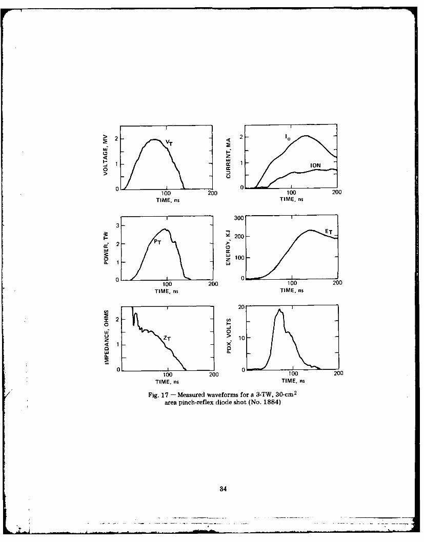
E. Small-Area Diodes
A modification to the diode design was tested to evaluate the performance
of smaller-radius diodes with larger ion-current source densities. The hollow
taper cathode, shown in Fig. 4, was configured to vary in radius. Shots were
taken at 100 cm2, reported above, and at 30-cm 2 area (see Fig. 4b).
Several small-area diode shots were taken at anode-cathode spacings from
2.6 to 5.6 mm. The small anode-cathode spacings shorted early in the pulse
while the large spacings caused the power to dissipate in the lower-impedance
vacuum feed. An intermediate spacing of 3.5 mm lead to efficient coupling of
the injected energy into the diode without shorting or power loss in the
structure. In this case, the diode impedance history was 1. z for 50 ns
before collapsing (see Fig. 17). A source-area-averaged ion current density
of 20 kA/cm 2 at peak power was obtained. The ion-current onset times for this
small-area diode were slightly earlier than for the large-area diode as
presented in Sec IV A.
33
2VT 2 10
~ 1 ION
0 0-100 200 100 200
TIME, ns TIME, ns
3003-
S200-E
0 0oo
100 200 100 200TIME, ns TIME, ns
20 20
wL 0
z ZT .10o41 x
0 0
0100 200 0100 200
TIME, ns TIME, ns
Fig. 17 - Measured waveforms for a 3-TW, 30-cm2
area pinch-reflex diode shot (No. 1884)
34
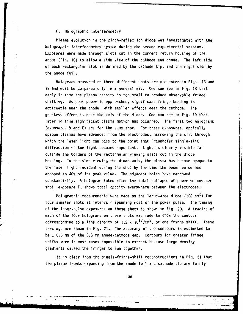
F. Holographic Interferometry
Plasma evolution in the pinch-reflex ion diode was investigated with the
holographic interferometry system during the second experimental session.
Exposures were made through slots cut in the current return housing of the
anode (Fig. 10) to allow a side view of the cathode and anode. The left side
of each rectangular slot is defined by the cathode tip, and the right side by
the anode foil.
Holograms measured on three different shots are presented in Figs. 18 and
19 and must be compared only in a general way. One can see in Fig. 18 that
early in time the plasma density is too small to produce observable fringe
shifting. As peak power is approached, significant fringe bending is
noticeable near the anode, with smaller effects near the cathode. The
greatest effect is near the axis of the diode. One can see in Fig. 19 that
later in time significant plasma motion has occurred. The first two holograms
(exposures D and E) are for the same shot. For these exposures, optically
opaque plasmas have advanced from the electrodes, narrowing the slit through
which the laser light can pass to the point that Fraunhofer single-slit
diffraction of the light becomes important. Light is clearly visible far
outside the borders of the rectangular viewing slits cut in the diode
housing. In the slot viewing the diode axis, the plasma has become opaque to
the laser light incident during the shot by the time the power pulse has
dropped to 40% of its peak value. The adjacent holes have narrowed
substantially. A hologram taken after the total collapse of power on another
shot, exposure F, shows total opacity everywhere between the electrodes.
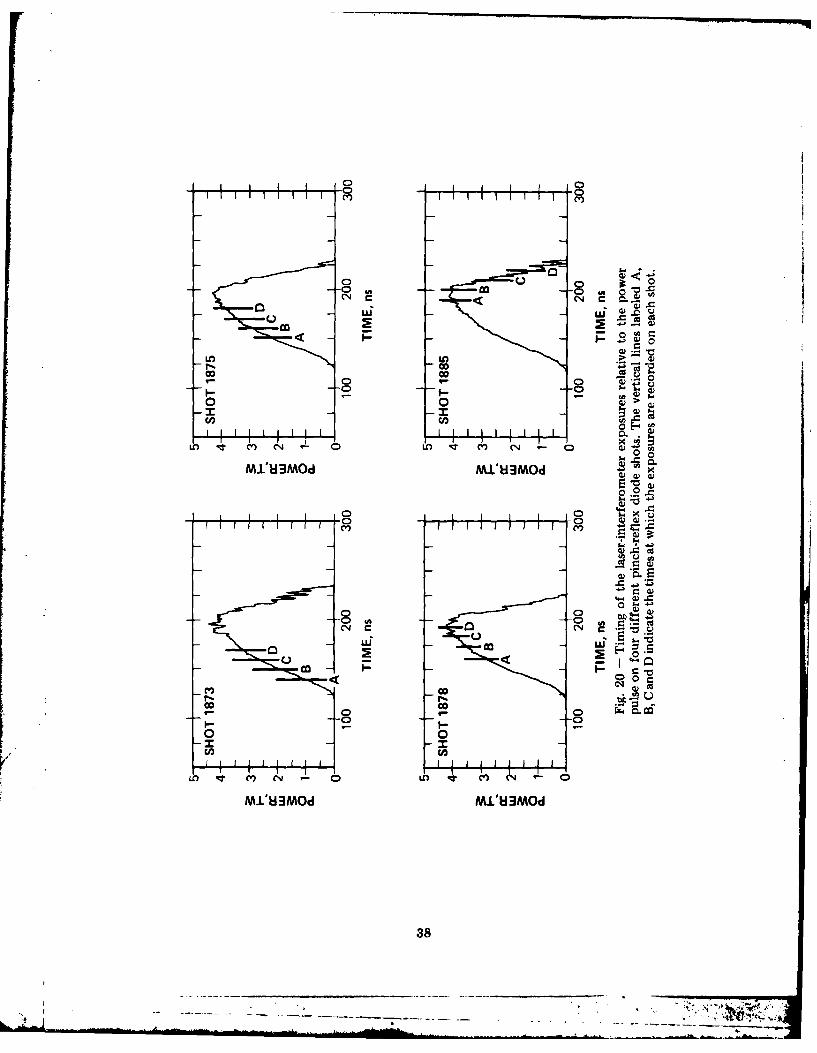
Holographic measurements were made on the large-area diode (100 cm2) for
four similar shots at interval- spanning most of the power pulse. The timing
of the laser-pulse exposures on these shots is shown in Fig. 20. A tracing of
each of the four holograms on these shots was made to show the contour
corresponding to a line density of 3.2 x 10¹⁷/cm2, or one fringe shift. These
tracings are shown in Fig. 21. The accuracy of the contours is estimated to
be ± 0.5 mm of the 3.5 mm anode-cathode gap. Contours for greater fringe
shifts were in most cases impossible to extract because large density
gradients caused the fringes to run together.
It is clear from the single-fringe-shift reconstructions in Fig. 21 that
the plasma fronts expanding from the anode foil and cathode tip are fairly
35
- - aumnnillnnl ' . -, .......

A B C
4- --
0CB
0.
100 200 300TIME, ns
Fig. 18 - Holograms showing plasma formation early in the power pulsefor the large-area diode. The timing of the laser-interferometer exposuresis indicated by the vertical lines labeled A, B and C on the correspondingpower pulse.
36

4-
3- D
D
I--
E- 1 I k 1100 200 300
TIME, ns
Fig. 19 - Holograms showing late-time plasma evolution for the large-areadiode. The timing of the laser interferometer exposures is indicated by thevertical lines labeled D, E and F on the corresponding power pulse.
37
-0 ---
CV 0.
IA I0N WNc 0
oc0
0
CA C
Ll It In LO IR )(
0in0.M1'83MOd M.±'U3MOd
0.2 -c
Q)0
E.)
LLII a
0 0
0 0 0
b CT Co C
M1IU3MOd M±L'U3MOd
38

0
00
'A) t6c
SoE Otb 0 q40 ,r
4
L. E
oo-
E s 0.0
00
r.)E 0
C&
Inn
39
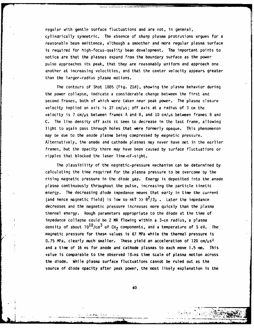
regular with gentle surface fluctuations and are not, in general,
cylindrically symmetric. The absence of sharp plasma protrusions argues for a
reasonable beam emittence, although a smoother and more regular plasma surface
is required for high-focus-quality beam development. The important points to
notice are that the plasmas expand from the boundary surface as the power
pulse approaches its peak, that they are reasonably uniform and approach one
another at increasing velocities, and that the center velocity appears greater
than the larger-radius plasma motions.
The contours of Shot 1885 (Fig. 21d), showing the plasma behavior during
the power collapse, indicate a considerable change between the first and
second frames, both of which were taken near peak power. The plasma closure
velocity implied on axis is 27 cm/ps; off axis at a radius of 3 cm the
velocity is 7 cm/us between frames A and B, and 10 cm/us between frames B and
C. The line density off axis is seen to decrease in the last frame, allowing
light to again pass through holes that were formerly opaque. This phenomenon
may be due to the anode plasma being compressed by magnetic pressure.
Alternatively, the anode and cathode plasmas may never have met in the earlier
frames, but the opacity there may have been caused by surface fluctuations or
ripples that blocked the laser line-of-sight.
The plausibility of the magnetic-pressure mechanism can be determined by
calculating the time required for the plasma pressure to be overcome by the
rising magnetic pressure in the diode gap. Energy is deposited into the anode
plasma continuously throughout the pulse, increasing the particle kinetic
energy. The decreasing diode impedance means that early in time the current
(and hence magnetic field) is low so nkT >> B2 /2p . Later the impedance
decreases and the magnetic pressure increases more quickly than the plasma
thermal energy. Rough parameters appropriate to the diode at the time of
impedance collapse could be 2 MA flowing within a 3-cm radius, a plasma
density of about 1018/cm3 of CH2 components, and a temperature of 5 eV. The
magnetic pressure for these values is 67 MPa while the thermal pressure is
0.75 MPa, clearly much smaller. These yield an acceleration of 120 cm/Us 2
and a time of 16 ns for anode and cathode plasmas to each move 1.5 mm. This
value is comparable to the observed lO-ns time scale of plasma motion across
the diode. While plasma surface fluctuations cannot be ruled out as the
source of diode opacity after peak power, the most likely explanation is the
40
...... . ..
ejection of plasma from the diode into the hollow cathode cavity and back to
the anode location by magnetic pressure from the diode short circuit.
In addition to the 3-TW, lO0-cm2 diode shots, several shots at 2 to 2.5-
TW diode power with a small-area (30 cm2) diode were holographically monitored
(Fig. 22). On Shot 1886 (Fig. 22a) interferograms of the diode during the
ascent to peak power were recorded, indicating little plasma motion before
peak power and with noticeable motion within a radius of 3 cm during the last
two frames at peak power. The closure velocity on axis between the last two
frames is 21 cm/ps.
On two other small-diameter shots, arcs occurred in different parts of
the feed early in tilne. On Shot 1879, the arc formed well upstream from the
diode in the coaxial vacuum feed. A perturbation in the reference fringes on
one side of the diode is the only indication of the event (Fig. 22b). On Shot
1380, the arc was in the diode, resulting from too small an electrode
separation. Tne diode was opaque to laser light even in the first hologram
and hence density contour inapping was not possible.
V. SUMMARY OF RESULTS
In this paper, we have presented recent technological advances in intense
pulsed ion-beam development. The pinch-reflex diode has been successfully
scaled up to multiterawatt operation on the PITHON accelerator. Pulsed proton
and deuteron beams have been produced in both planar and spherically focusing
geometries with 1.0-MA of 1.8-MeV light ions measured at a peak power of 1.8
TW yielding a 130-kJ light ion beam in 100 ns.
Focusing of intense ion beams by electrode shaping and by self-magnetic
field deflection has been shown at large radii to follow simple theoretical
modeling with several corroborating diagnostics. Spherical electrode shaping
served to compress the ion beam from an ll-cm-diam anode surface to a 3-cm-
diam focal spot located, due to magnetic bending, inside the geometric
focus. Small-area diode tests at lower power demonstrated that impedance
lifetime is not a problem at higher source-current-density levels. Further,
these results suggest that a smaller-area pinch-reflex diode of higher power
density may be suitable for injection into a plasma transport channel.
The most serious problem encountered in these experiments was independent
41
L . ,-

3.5 mm
5 I I
I I1879SHOT 1886
44A
C 33-A oC
2
I
0
c
0-- 1
100 200 300 100 200 300
TIME, fls TIME, ns
(a) SHOT 1886 (b) SHOT 1879
Fig. 22 - Single-fringe-shift reconstructions for (a) Shot 1886 and (b) Shot 1879.The timing of the laser interferometer exposures is indicated by the vertical lineslabeled A, B, C and D on the corresponding power pulses. The shaded regions in-dicate plasma line densities greater than 3.2 X 10¹⁷ /cm 2 .
42
i_ - - -
of the pinch-reflex diode but concerned the coupling of power from the
accelerator interface through the vacuum feed structure to the diode. These
losses were found to be geometric, that is, independent of electrode surface,
and occurred principally between the biconic-to-coax transition and the
diode. Reducing the early-time diode impedance, smoothing the vacuum feed of
resonant grooves, and enhancing the cathode emission tip all served to
increase the power flow to the diode.
Beam diagnostics were developed to survive the harsh bremsstrahlung and
impulse environment of a 3-TW pinch-reflex diode. Measurements of nuclear-
reaction products provided total ion yields and pulse-shape evaluations.
Total beam Rogowski coil monitors were developed to perform through the time
of peak power. The shadowbox technique provided beam-focus location and
local-beam divergence.
A first study of the spatial evolution of the anode and cathode plasmas
in a 3-TW pinch-reflex diode was performed on multiple shots spanning the
power pulse. Surfaces at constant line density (3 x 10¹⁷/cm2) are observed to
expand from the electrodes at times approaching peak power in fairly uniform
though nonsymmetric profiles and accelerate toward one another. After peak
power, significant anode-plasma surface fluctuations and a high velocity (up
to 30 cm/us) axial plume were observed. During the power pulse collapse a
high density (n > 1018/cm3) plasma bridges the anode-cathode gap over the
central 7.5-cm diameter. On some shots the high density plasma is later seen
to open suggesting magnetic plasma confinement. The knowledge of the anode
and cathode shapes at peak power suggests that further research into the
formation of more uniform plasmas is necessary for development of a highly
focused ion diode. The measured evolution of the shapes of the anode and
cathode plasmas is the information required to design a first iteration
modification to the simple spherically focusing anode.
43
F-

REFERENCES
1. See for example: G. Yonas, 4th ANS Topical Meeting on Technology of
Controlled Nuclear Fusion, October 14-17, 1980, Valley Forge,
Pennsylvania; and S. Humphries, Jr., SAND 80-0402, Sandia Laboratories,
1980.
2. G. Cooperstein, S.A. Goldstein, D. Mosher, R.J. Barker, J.R. Boiler, B.G.
Colombant, A. Drobot, R.A. Meger, W.F. Oliphant, P.F. Ottinger, F.L.
Sandel, S.J. Stephanakis, and F.C. Young, in Laser Interaction and Related
Plasma Phenomena, H. Schwarz, H. Hora, M. Lubin and B. Yaakobi, Editors
(Plenum, New York, 1981), Vol. 5, p. 105.
3. V.M. Bystritsky and A.N. Didenko, Uspekhi Fizicheskikh Nauk 132, 91
(1980).
4. J.W. Shearer, Nucl. Fusion 15, 952 (1975).
5. M.j. Clauser, Phys Rev. Lett. 35, 849 (1975).
6. R.O. Bangerter and D.J. Meeker, in Proc. 2nd Int. Topical Conf. on High
Power Electron and Ion Beam Res. and Tech.,J.A. Nation and R.N. Sudan,
Editors, (Cornell University, Ithaca, New York, 1977), p. 183.
7. J. Maenchen, L. Wiley, S. Humphries, Jr., E. Peleg, R.N. Sudan, and D.A.
Hammer, Phys. Fluids 22, 555 (1979).
8. S.A. Goldstein, G. Cooperstein, Roswell Lee, D. Mosher and S.J.
Stephanakis, Phys. Rev. Lett. 40, 1504 (i978).
9. S. Humphries, Jr., J. Appl. Phys. 51, 1876 (1980).
10. P.F. Ottinger, D. Mosher, and S.A. Goldstein, Phys. Fluids 23, 909 (1980).
11. D. Mosher, G. Cooperstein, S.J. Stephankis, S.A. Goldstein, D.G.
Colombant, and Roswell Lee, Report No. 3658, Naval Research Laboratory,
1977.
12. G. Frazier, in Proc. NSWC Pulse Power Systrins Workshop (Cornell
University, Ithaca, New York, Sept. 1976).
13. D. Mosher, D. G. Colombant, and S.A. Goldstein, Comments Plasma Phys. 6,
101 (1981).
14. 0. Mosher, Bull. Am. Phys. Soc., Ser. II, 25, 900 (1980).
15. D.G. Pellinen, Marco S. DiCapua, S.E. Sampayan, H. Gerbracht, and M. Wang,
Rev. Sci. Instrum. 51, 1535 (1980).
44
.....

16. A. Drobot, Roswell Lee, S.A. Goldstein, and G. Cooperstein, IEEE Conf.
Record Abstracts, 1979 IEEE Int. Conf. on Plasma Sci. (Montreal, Canada,
June 4-6, 1979), IEEE No. 79CH1410-0 NPS, p. 78.
17. F.C. Young, W.F. Oliphant, S.J. Stephanakis, and A.R. Knudson, IEEE Trans.
Plasma Sci. PS-9, 24 (1981).
18. F.C. Young, IEEE Trans. Nuc1. Sci. NS-22, 718 (1975).
19. H. Liskien and A. Paulsen, Nuclear Data Tables 11, 569 (1973).
20. H.W. Lefevre, C.A. Burke, and R.M. Bahnsen, Report No. RLO-1925-44,
University of Oregon, 1971.
21. H.H. Andersen and J.F. Ziegler, Stopping Powers and Ranges in all
Elements, (Pergamon Press, New York, 1977), Vol. 3.
22. J.G. Pronko, T.R. Fisher, and L.F. Chase, Nuc1. Instr. and Meth. 163, 227
(1979).
23. F.C. Young, D. Mosher, S.J. Stephankis, S.A. Goldstein, and D.
Hinshelwood, Memo Report No. 3823, Naval Research Laboratory, 1978.
24. K. Triebes and R. Huff, Bull. Am. Phys. Soc., Sec. II, 19, 976 (1974).
25. D. Mosher, G. Cooperstein, and S.A. Goldstein in Technical Digest of Conf.
on Inertial Confinement Fusion (San Diego, California, February 26-28,
1980), IEEE No. 80CH1536-2 QEA, p. 104.
26. A.E. Blaugrund, G. Cooperstein and S.A. Goldstein in Proc. Int. Topical
Conf. on Electron Beam Res. and Tech. G. Yonas, Editor, SAND76-5122,
(Albuquerque, New Mexico, Feb., 1976) Vol. I, p. 233.
27. R.D. Genuario and V.L. Bailey, Appl. Phys. Lett. 33, 694 (1978).
28. J.C. Martin "Nanosecond Pulse Techniques," SSWA/JCM/704/49, Internal
Report, AWRE, Aldermaston, England, 1970.
29. H.W. Koch and J.W. Motz, Rev. Mod. Phys. 31, 4 (1959).
30. F.C. Young, S.J. Stephanakis, G. Cooperstein, D. Mosher, F.L. Sandel, P.G.
Slauner and S.A. Goldstein, Naval Research Laboratory Report 4322, 1980.
31. E. Nardi, E. Peleg and Z. Zinamon, Appl. Phys. Lett. 39, 46 (1981).
32. J. Creedon, J. Appl. Phys. 48, 2946 (1975).
4 5/f4,
_ _ _ _ _ _ _I ***

DISTRIBUTION LIST AUGUST 1981
Director CommanderDefense Intelligence Agency Harry Diamond LaboratoriesWashington, OC 20301 2800 Powder Mill Road
Adelphi. MD 20783Attn: DTICI Robert 1. Rubenstein I copy (CNWDI-INNER ENVELOPE: ATTN: DELHD-RBH)
Attn: DELHD-NP I copy
Defense Advanced Research Project Agency DELHD-RCC J. A. Rosado I copy1400 Wilson Blvd. DRXDO-RBH P. A. Caldwell 1 copy
Arlington, VA 22209Attn: J. Bayless I copy DRXDO-TI Tech Lib. I copy
S. Graybill 1 copy
DirectorDefense Nuclear Agency CommanderWashington. DC 20305 Picatlnny Arsenal
Attn: FCPR I copy Dover, NJ 07801
STVL I copy Attn: SNUPA ND-N-E I copyTISI Archives 1 copyTITL Tech. Library 3 copiesJ. Z. Farber (RAEV) I copy U. S. Air Force Office of Scientific ResearchR. L. Gullickson (RAEV) I copy Physics Directorate
Bolling A.F.B., DC 20332
Defense Technical Information Center Attn: A. K. Hyder I copyCameron Station 14. A. Stroscio 1 copy5010 Duke StreetAlexandria, VA 22314
CommanderAttn: T. C. 12 €opie U.S. Army Missile Comnand
Redstone Arsenal. AK 35809
Under Sec'y of Defense for RSCH and ENGRG Attn: Redstone Scientific Information CTRDepartment of Defense DRCPM-PM-PE-EA 1 copyWashington, DC 20301
Attn: S&SS(OS) I copy CommamnderU. S. Army Nuclear Agency
Chief 7500 Backlick RoadLivermore Division Fld Command DNA Building 2073Lawrence National Laboratory Springfield, VA 22150P. 0. Box 808Livermore, CA 94550 Attn: ATCN-W I copy
Attn: FCPRL I copyCommanderU. S. Army Test and Evaluation COMO
National Technical Information Service Aberdeen Proving Ground, MD 21005
U.S. Department of Commerce Attn: ORSTE-EL I copy5285 Port Royal Road
Springfield, VA 22161 24 copiesCommander
Comnder Naval Electronic Systems CMD HQSISystem Command Washington, DC 20360
P. 0. Box 1500 Attn: Code 5032 ! copyHuntsville, AL 35807
Attn: SSC-TEN I copy Commanding OfficerNaval Intelligence Support Center4301 Suitland Road - Building 5
DEP Chief of Staff for RSCH DEV & ACQ Washington, DC 20390
Department of the Army
Washington, DC 20310 Attn: NISC-45 I copy
Attn: DAMA-CSM-N 1 copy
47
i~

Naval Research Laboratory SARLO/DYAddressee: Attn: Name/Code Post Office Box 92960
Code 2628 - TIC-Distribution 25 copies WorIdway Postal CenterCode 4040 - J. Boris 1 copy Los Angeles, CA 90009Code 6682 - D. Nagel I copy (Technology)Code 4700 - T. Coffey 26 copietCode 4707 - J. Davis I copy Attn: DYS I copyCode 4730 - S. Bodner I copyCode 4740 - V. Granatstein I copyCode 4760 - B. Rooson 1 copyCode 4761 - C. Kapetanakas I copy SAMSO/INCode 4770 - Branch Head 10 copies Post Office Box 92960Code 4770 - F. Young I copy Worldway Postal CenterCode 4770 - S. Stephanakis 1 copy Los Angeles, CA 90009Code 4771 - 0. Mosher 10 copiesCode 4773 - G. Cooperstein 10 copies Attn: IND NAJ D. S. Ruskin 1 copyCode 4790 - 0. Colombant I copyCode 4790 - I. Haber I copyCode 4790 - M. Lampe I copy SAMS0/MN
On-Site Contractors: Norton AFB. CA 92409
Code 4770 - R. Barker (Jaycor) I copy (Minuteman)Code 4770 - S. Goldstein (Jaycor) I copyCode 4770 - R. Meger (Jaycor) I copy Attn: MNNH 1 copyCode 4770 - P. Ottinger (Jaycor) 1 copyCode 4770 - F, Sandel (Jaycor) I copyCode 4790 - A. Orobot (SAI) I copy SAHSO/SK
Post Office Box 92960Worldway Postal CenterLos Angeles, CA 90009Officer-tn-Charge (Space Comm Systems)
Naval Surface Weapons CenterWhite Oak, Silver Spring, MD 20910 Attn: SKF P. H. Stadler I copy
Attn: Code WR43 I copyCode WASOI - Navy Nuc Prgms Off I copy U. S. Department of Energy
Division of Inertial Fusion
Chief of Naval Operations Washington, DC 20545
Navy Department Attn: G. Canavan I copyWashington, DC 20350 T. F. Godlove 1 copy
S. L. Kahalas I copyAttn: R. A. Blaise 604C4 I copy R. L. Schriever I copy
Commander U.S. Department of EnergyNaval Weapons Center P.O. Box 62China Lake, CA 93555 Oak Ridge, TN 37830 50 copies
Attn: Code 533 Tech Lib. I copyArgonne National Laboratory
A s o9700 South Cass AvenueAF Weapons Laboratory, AFSC Argonne. Illinois 60439
Kirtland AFB, NM 87117Attn: G. R. Magelssen I copy
Attn: CA I copy R. J. Martin I copyELC I copyNT "copySOL 1 copy Brookhaven National LaboratoryDYP I copy Upton, NY 11973J. Darrah I copyL.L. Baker I copy Attn: A.F. Maschke 1 copy
HQ USAF/RDWashington, DC 20330
Lawrence Berkley LaboratoryAttn: RDQSM I copy Berkeley, CA 94720
Director Attn: D. Keefe I copy
Joint Strat TGT Planning Staff JCSOFFUTT AFBOuha, NO 68113Attn: JSAS I copy
48

Lawrence Livermore National Laboratory Bechtel Group. Inc.P. 0. Box 808 P.O. Box 3965Livermore. CA 94550 San Francisco, CA 94119
Attn: L-18 I copy Attn: W. 0. Allen 1 copyL-153 I copyR. J. Briggs 1 copyE. P. Lee 1 copy Boeing Company, The
J. H. Nuckolls I copy P. 0. Box 3707S. S. Yu I copy Seattle, WA 98124Tech Info Dept. L-3 I copyO.J. Meeker I copy Attn: Aerospace Library I copyA.B. Langdon 1 copyE. Teller I copyD.S. Prono 1 copy Cornell University
Ithaca, NY 14850
Los Alamos National Laboratory
P. 0. Box 1663 Attn: D. A. Hammer I copyLos Alamos, NM 87545 R. N. Sudan 1 copy
J. Maenchen 1 copyAttn: D. B. Henderson 1 copy J.B. Greenley 1 copy
R. B. Perkins I copy C.8. Wharton I copyL. E. Thode 1 copyC. Barnes I copyD. Forslund 1 copy The Dikewood CorporationR.O. Bangerter 1 copy 1613 University Blvd., NEW.P. Gula I Copy Alburquerque, NM 87102
National Science Foundation Attn: L. Wayne Davis I copyMail Stop 19Washington, DC 20550
EG&G, Inc.Attn: D. Berley I copy Albuquerque Division
P. 0. Box 10218Sandia National Laboratories Albuquerque, NM 87114P. 0. Box 5800Albuquerque, NM 87185 Attn: Technical Library I copy
Attn:
J. R. Freeman / 4241 1 copy Electric Power Research InstituteS. Mumphries / 4253 1 copy 3412 Hillview Avenue0. J. Johnson / 4244 1 copy P.O. Box 10412G. W. Kuswa / 4240 1 copy Palo Alto, CA 94303P. A. Miller / 4244 1 copyJ. P. Vandevender / 4252 1 copy Attn: K.W. Billman I copy
G. Yonas / 4200 1 copyDoc Con for 3141 Sandia RPT Coll 1 copyJ.N. Olsen / 4244 1 copy Ford Aerospace & Communications OperationsG.A. Allshouse / 4247 1 copy Ford A Jamboree Roads
T.A. Mehlhorn / 4247 1 copy Newport Beach, CA 92663N.N. Widner / 4247 1 copy (Formerly Aeronutronic Ford Corporation)T.P. Wright / 4241 1 copyJ.P. Quintenz / 4241 1 copy Attn: Tech Info Section 1 copyP.L. Mix / 4242 1 copyC.W. Mendel /4244 1 copy
A.V. Farnsworth / 4247 1 copy General Electric CompanyM.A. Sweeney / 4247 1 copy Space Division0.B. Seidel / 4241 1 copy Valley Forge Space Center
Goddard Blvd.. King of Prussia
AVCO Research and Systems Group P. 0. Box 8555
201 Lowell Street Philadelphia, PA 19101
ilmington, mA 01887 Attn: J. C. Penden VFSC, Rm. 4230M 1 copy
Attn: Research Lib. A830 Rm. 7201 1 copy
General Electric Company
SON Corporation, The Tempo-Center for Advanced Studies
795 Jones Branch Drive 816 State Street (P. 0. Drawer QQ)
McLean, VA 22101 Santa Barbara, CA 93102
Attn: Tech Lib. I copy Attn: DASIAC I copy
49

Grumman Aerospace Corporation Maxwell Laboratories, Inc.Bethpage, NY 11714 9244 Balboa Avenue
San Diego, CA 92123
Attn: P. Suh I copy Attn: R. W. Clark 1 copy
A. C. Kolb 1 copy
Institute for Defense Analyses A. Korn I copy
400 Army-Navy Drive A. Peailler I copy.1. Peariman i copyArlington, VA 22202 J. Shannon I copy
Attn: IDA Librarian R S. Smith 1 copy
McDonnell Douglas CorporationIon Physics Corporation 5301 Bolsa AvenueSouth Beford Street Huntington Beach, CA 92647
Burlington, MA 01803 Attn: S. Schneider I copy
Attn: H. Milde I copy
Mission Research Corporation1400 San Mateo Blvd. SEAlbuquerque, NM 87108
IRT CorporationP. 0. Box 81087 Attn: B. B. Godfrey I copy
San Diego, CA 92138
Attn: R. L. Mertz 1 copy Mission Research Corporation-San DiegoP. 0. Box 1209
JAYCOR, Inc. LaJolla, CA 92038
205 S. Whiting Street Attn: V.A.J. Van Lint I copy
Alexandria, VA 22304
Attn: E. Alcaraz 1 copy Mission Research CorporationJ. Guillory I copy 735 State Street
R. Hubbard I copy Santa Barbara, CA 93101It. Sullivan I copy0. A. Tidman I copy Attn: W. C. Hart I copy
C. L. Longmire I copy
JAYCOR. Inc.11011 Torreyana Road Northrop Corporation
San Diego, CA 92121 Electronic Division2301 West 120th Street
Attn: E. Wenaas 1 copy Hawthorne, CA 902503.5. Wang I copy
Attn: V. R. DeMartino I copy
Kaman Science CorporationP. 0. Box 7463 Northrop CorporationColorado Springs, CO 80933 Northrop Research an,! Technology Ctr.
3401 West BroadwayAttn: A. P. Bridges I copy Hawthorne, CA 90205 1 copy
D. H. Bryce I copyJ. R. Hoffman 1 copyW. E. Ware I copy Physical Dynamics
P.O. Box 556La Jolla, CA 92031
Lockheed Missiles and Space Co., Inc.3251 Hanover Street Attn- S. Jorna I topyPalo Alto, CA 94304
Attn: L. F. Chase I copy Physics International Co.
2700 Merced Street
Massachusetts Institute of Technology San Leandro. CA 94577
Cambridge, MA. 02139 Attn: J. Benford I copy9. BernsteinI copy
Attn: R.C. Davidson I copy G. Frtzier I copyG. Bekefi I copy E. B. Goldman 1 copyD. Hinshelwood I copy R. Huff copy
A. J. Toepfer I copy
G. Dahlbacka copy
50
-. -" _
Power Conversion Technology. Inc. Systems, Science and Software. Inc.1158 Sorrento Vally Road P. 0. Box 1620San Deigo, CA 92121 LaJolla, CA 92038
Attn: V. Fargo 1 copy Attn: A. R. Wilson I copyD.A. Phelps I copy
Texas Tech UniversityPrinceton Plasma Physics Laboratory P. 0. Box 5404 North College StationJames Forrestal Campus Lubbock, TX 79417P.O. Box 451Princeton, N.J. 03540 Attn: T. L. Simpson 1 copy
M. Kristiansen 1 copyAttn: R. Kulsrud 1 copy
Pulse Sciences. Inc. TRW Defense and Space Sys Group
1615 Broadway, Suite 610 One Space Park
Oakland. CA 94612 Redondo Beach, CA 90278
Attn: I. Smith 1 copy Attn: Teci Info Center/S-1930 I copy
P. Spence 1 copy Z.G.T. Guiragossian I copyS. Putnam ! copy 0. Arnush I copy
R&D Associates University of California
P. 0. Box 9695 Dept. of PhysicsMarina Del Rey, CA 90291 La Jolla, CA 92037
Attn: W. R. Graham, Jr. I copy Attn: K. Brueckner 1 copy
M. Grover I copy W.B. Thompson I copy
C. MacDonald I copyE. Nartlnelli 1 copy University of California
Boelter Hall 7731
Los Angeles, CA 90024
R&D AssociatesSuite 500 Attn: F.F. Chen 1 copy1401 Wilson Blvd.Arlington, VA 22209 University of California
Attn: P. J. Turchi I copy Irvine, CA 92717
Attn: G. Benford I copyScience Applications, Inc. N. Rostoker I copyP. 0. Box 2351 S. Robertson 1 copy
LaJolla, CA 92038 A. Fisher I copy
Attn: J. Robert Beyster I copy University of Illinois
Urbana, IL 61801Spire CorporationP. 0. Box 0 Attn: G. H. Miley 1 copy
Bedford, MA 01730 J. T. Verdeyen I copy
Attn: R. G. Little I copy University of Rochester
Laboratory of Laser Energetics
SRI International River Station, Hopeman 110
333 Ravenswood Avenue Rochester, NY 14627Menlo Park, CA 94025 Attn: Director 1 copy
Attn: S. Odairiki I copyR.J. Vidmar I copy
University of Scranton
Dept. of PhysicsStanford University Scranton, PA 18510SLACP. 0. Box 4349 Attn: F. Murray 1 copyStanford, CA 94305
Attn: W. B. Herrinannsfeldt I copy
51
I •'

Univ. of WashingtonDept. of Nuclear EngineeringOF-10Seattle, WA 98115
Attn: F. Ribe I copy
Univ. of Wisconsin
Dept. of Nuclear EngineeringIS0o Johnson DriveMadison. WI 53706
Attn: G.A. Moses I copy
G.L. Kulcinski I copy
Vought CorporationMichigan Division38111 Van Dyke RoadSterling Heights. MI 48077
(Formerly LTV Aerospace Corp)
Attn: Tech Lib 1 copy
Westinghouse Electric Corporation
Research and Development Center1310 Beulah RoadPittsburgh, PA 15235
Attn: M.D. Nahemow 1 copy
Atomic Weapons Research Establishment
Building H36Aldermaston. Reading RG 7 4PR
United Kingdom
Attn: j. C. Martin 1 copy
52
A ll .. ... Il .. .