lib.tkk.filib.tkk.fi/diss/2013/isbn9789526053905/isbn9789526053905.pdfthe present thesis was a part...
TRANSCRIPT
��������� ����
���������� ���������������� ������������������������������������������������������������������������ ��������������������������� ���������� ���������������������������
������������ !�!�"���#$�������%�����# &�$� $�#���� ��� ����$� &�!'!%"�� #!��!(�#���! $!#�'������#$�$�!���
�����
��
�� ��
����
���������
����
�������������������������������������
����������
����������� ����
���� ���������� ���������������
����������� �����������������������������������
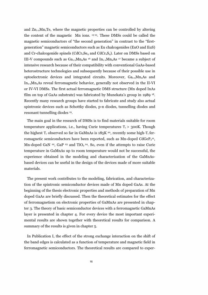
�������'�)������
�! $!#�'������#$�$�!���

��������� ��������������� �������������������� �����������
����������� ��������������������������������
��������������
����� ������� ������� �������� ����������� ���� ������!���������������� �������"��������� #����������� ���������$���� ����$��� ���� ��������%�#�������������������&� ��� �#� �'�������(� ��������������������� ���� ���������$���� ����$��� ��)$����*�+���,��������-������.���#�� ��������������/�
���������������������������������������������� ���!�����"������� �������������������#������$��%

�% �������� ��������0 ������ �0�11��2�������
�������������� /� � ����.��1���
#����!������&�!�����0 ������ �(�����3���� *�&14������ ���*� "����0 ������ �5�����������*�6!!�7�� #�������������*�+����
� �����0 ������ �8�����9��� ���1�*�:����1���#*�+����
��������� ��������������� �������������������� �����������
;�.������&��������
7 <.�=>�?=-�?��?-��=?=�7 <.�=>�?=-�?��?-�=�?-�)���,�7 .?&��>==?@=�@�7 .��>==?@=�@�)� ���,�7 .��>==?@=@��)���,�����A��� /���8.A7 <.A=>�?=-�?��?-�=�?-�
�� ����B��'���1������
+����

�����������������������'#(�()�&**+++',-+++./�����000(�����(��
�%������������������� �!������������������������������������� ��������������������������������
#%���������������������������������
���������� ����������������������
�������������������������������������� !" #���$���#"�"$ ��%&'()*%+
,���������������� �����������������
"��%���� ��%�!�����%,-���)*%+ ����������������%.���� ���)*%+
#��!�������� %������������1����2)/������)*%+ ����%����������
"������ � �������������������1�%!!���3����������������2
��������"���������������������0��1���������������2����� ��������������������������
�������������������������������������������������������������� �������������������������������������������������1���� �������3"���������������24������������������� ��������������������������������5����� ����������������������������������2���������0��������6�������2���6�07����������������2������������������������2�������� ���������������������������������������������� ������5����� ����3"�� ��������������������������������8�����������������9�������������5���2�����:�����������9���������24�������4�������� ���������� ���������5����� ��������������������������������������������4������5����� �������������������������3"���4����������������������������������������������������������������������������������������������� �����3"�� �������������������������0������������������������������������� ����������������������������������������� ������������������ ����������������������� ���������������� ������������ ������� �����������3"�� ��������������� ������5����� ������������:����0��6������������������������������� ���������3$�����1���� ��������������4��6�������� ������������ �2��0;�������2���6�07����������������2�����6�������2���������������������������4�������������������������<�� �����1������5�����������4������������������������3"������������� �����������������������������4������������ �����������$0=������������2>��������2 ���������������2��� ������8������������������� ����������� ����������3"�� ���������4����������������������������������������� ��������������������?"��#@��������6�07����������������������������������������������3"�������4������������������4������������24��� ��������4��������8��������������40��4�����������������3"����������� ������1���������� ������� �������������������������3�����1� ���2���������������0����������������� ���������5���������������� ���4�������������4������ ������������������������������ ������������������������������������4����� ����������� ����������������3
4��0��������������2������ ��������2�� �����������������2 ���������������2����������������
�) 1 ������2/A'0/.)0&*0.+'/0/ �) 1 ��2/A'0/.)0&*0.+/*0.
�� -�%A//0,/+, �� 1 ������2%A//0,/+, �� 1 ��2%A//0,/,)
���������� %�������>�����6� ���������� �������>�����6� 5���)*%+
#����%A* %������B((���3�(�#�B$�<�B/A'0/.)0&*0.+/*0.


���������!6�����-���� ����'#�**+++'+++./�����000(�����(��
��7�86���������������96��:�7��8����!����������������������������0����6����������� �����������������6�������;����6� ��������
;%�7����8��C�6D��6���6��6��6��6����
57��77:��6��0;�������6���6��������
���8��������������������������������� !" #���$���#"�"$ ��%&'()*%+
�%�7�!%����E����;������6�������
46��7��8���%7��� �!%,3*&3)*%+ 96��:� 6��6%.3%%3)*%+
;%�7���%�%���!�:��6!�� 6��6)/3*'3)*%+ 4������������
"��������� 5�������!6�6��:�7��8�1����������-���3�����������77����2
���������!6"�D��C���6��������������������;�6�6������������� �66�����������������6���6���2 �����������;C�;���C��� ����2;�����0��6��������������6���6�������������6�������;����6� �����������C�6D�����6��;����� �������6����3 ������������������6����;��6� �����������6���������� �����������������������06������������� �����������6�����������3"��6����;�6� ��������;���������0�����6���2�����6�0������2�������6�07����0�������������2�����������������������2;������ ������������6������0���������������������6�����6�����0������������3:� ���������� �������6�����6C������������������6�����6���66��26����:������������������6������2 �6C �������������6��6����������������� �������6���2;��������������� ���� 3�����������6����6������ �6������������6����;�������������;������C �����3������������������� �66����������6���6��;����;����������C���������6��;������ �D��C26���� ������������������;��������C������������������� ����2��������������� ���������������������������C����������C;���6����� ��������6���C����6��������3���������� �������������6����������������������:����0��������C6����6�����������������6��6������C �D0��������3"�D�6�6������������������� �������������������������6�������;����6� ��������;�6��������� ���������������;�6C���C������6��������6�0��6���66�� �������������������;������0����6����;��6������6�����3:� �����������C�6D���C;� ������������ �������6������6������ ����� ����$0=� �����6C��C�2>����� �D2 �����������������;� �����������C �D�����;� ��������6���C����6�����3"C�6�������������C�������������������� �����������������0�� �D��D��� �������6�07����0����������������;������ ���������������������������������������3$� �D���������� �D�������������C;C���������C2 �6C������������� ����������������������������������������6��6� �����������������6���3"�D��C6�������������������� �������������C��������� �������C�6D������ �D�3��� ��6�6������0��C;C�;������������� ����6��������6������0�����������������0����6�������� ����������������������;� ���������������������;�����C �D����0��������;�6��6���� �����6�����6C��������C ��������6����C��������3
��������������������66�2������ ��������2�����;������6�������2 �����������������2�����������0�� �D�
�) 1 ������%2/A'0/.)0&*0.+'/0/ �) 1 ��2/A'0/.)0&*0.+/*0.
�� -�%A//0,/+, �� 1 ������%2%A//0,/+, �� 1 ��2%A//0,/,)
;%�7���% ��77�>�����6� #���� ��77�>�����6� 9%���)*%+
���%!66�6%A* %������B((���3�(�#�B$�<�B/A'0/.)0&*0.+/*0.


7
PrefaceThe research work for this doctoral dissertation was carried out in the Electron
Physics Group in the Department of Micro and Nanosciences at the Aalto Uni-
versity School of Electrical Engineering (formerly Helsinki University of Tech-
nology). I wish to express my gratitude to my supervising professor, Professor
Pekka Kuivalainen, for the opportunity to work in the group and for his advice
and guidance in the modeling part of the work. The experimental part of the
work was conducted under the supervision of Dr. Sergey Novikov. I am much
obliged to him for his committed support and advice during the work.
The present thesis was a part of the projects “New semiconductor devices for
spintronics” and “Room temperature spintronics” funded by the Academy of
Finland during 2002-2007. Also the financial support from the Dean of the
School of Electrical Engineering, Professor Tuija Pulkkinen, to finalize the the-
sis during 2012-2013 is appreciated.
I wish to thank all my co-authors for their contribution and pleasant collabora-
tion. I am especially grateful to Dr. Heikki Holmberg for the joint journey to
the world of accurate measurements at low temperatures. I wish to thank Pro-
fessor Magnus Willander and Professor Jouni Ahopelto for pre-examing this
dissertation and Professor Ronald Österbacka for agreeing to act as the oppo-
nent at the public examination of the dissertation. I also would like to thank Ms
Charlotta Tuovinen for revising the language of my publications. In fact, I wish
to express my gratitude to all my co-workers in the Electron Physics Group, but
especially to Professor Hele Savin for the working opportunities and her sup-
port during the last few years.
Last, but not least, I am very grateful to my family, my husband Dmitry and my
children Alexey and Ilia, for their love and support, encouragement and under-
standing throughout my studies.
Natalia Lebedeva
Espoo 16.3.2013

8
Contents
Preface ...............................................................................................................7
Contents ........................................................................................................... 8
List of publications ........................................................................................... 9
Author’s contribution......................................................................................10
List of Abbreviations ....................................................................................... 11
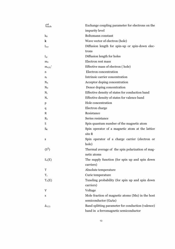
List of Symbols ................................................................................................12
1 Introduction ............................................................................................15
2 Diluted magnetic semiconductors ..........................................................18
2.1 General ..................................................................................................18
2.2 Growth of GaMnAs thin films................................................................18
2.3 Energy band structure of GaMnAs ........................................................21
3 Modeling of the material parameters for GaMnAs thin films ............... 23
3.1 Corrections to the band energies......................................................... 23
3.2 Charge carrier mobility and recombination ......................................... 26
4 Semiconductor devices with a GaMnAs layer: theoretical modeling vs.
experiments ................................................................................................... 30
4.1 Schottky diode....................................................................................... 30
4.2 P-N diode .............................................................................................. 36
4.3 Ferromagnetic Esaki-Zener Tunnelling diode...................................... 40
4.4 Magnetic resonant tunnelling diode..................................................... 47
4.5 Ferromagnetic quantum dots ................................................................57
5 Summary ................................................................................................ 64
6 References .............................................................................................. 66

9
List of PublicationsThis thesis consists of an overview and the following publications which are
referred to in the text by their Roman numerals.
I. N. Lebedeva and P. Kuivalainen, Shift in the absorption edge due to ex-
change interaction in ferromagnetic semiconductors, Journal of Phys-
ics: Condensed Matter, vol. 14, pp. 4491-4501, 2002.
II. N. Lebedeva and P. Kuivalainen, Modeling of ferromagnetic semicon-
ductor devices for spintronics, Journal of Applied Physics, vol. 93, pp.
9845-9864, 2003.
III. H. Holmberg, N. Lebedeva, S. Novikov, J. Ikonen, P. Kuivalainen, M.
Malfait, and V. V. Moshchalkov, Large magnetoresistance in a ferro-
magnetic GaMnAs/GaAs Zener-diode, Europhysics Letters, vol. 71, pp.
811-816, 2005.
IV. H. Holmberg, N. Lebedeva, S. Novikov, P. Kuivalainen, M. Malfait and
V. V. Moshchalkov, Electrical transport in Mn-doped GaAs pn-diodes,
Physica Status Solidi (a), vol. 204, pp. 791-804, 2007.
V. H. Holmberg, G. Du, N. Lebedeva, S. Novikov, P. Kuivalainen and X.
Han , Magnetotransport in ferromagnetic Schottky diodes made of Mn-
doped GaAs, Journal of Physics: Conference Series, vol. 100, p.
052075, 2008.
VI. H. Holmberg, N. Lebedeva, S. Novikov, M. Mattila, P. Kuivalainen, G.
Du, X. Han, M. Malfait and V. V. Moshchalkov, Magnetotransport of
holes through an AlAs/GaAs/AlAs resonant tunnelling quantum well
with a ferromagnetic Ga1-xMnxAs emitter, Physica Status Solidi (a), vol.
204, pp. 3463-3477, 2007.
VII. N. Lebedeva and P. Kuivalainen, Spin-dependent current through a
ferromagnetic resonant tunnelling quantum well, Physica Status Solidi
(b), vol.242, pp. 1660-1678, 2005.
VIII. N. Lebedeva, H. Holmberg and P. Kuivalainen, Interplay between the
exchange and Coulomb interactions in a ferromagnetic semiconductor
quantum dot, Physical Review B, vol. 77, p. 245308, 2008.
10
Author’s contribution
Publication I: The author has derived the equations of the model, written the
computer code, analyzed the results and written the manuscript.
Publication II: The author has derived most of the equations of the model,
written the computer code, and analyzed the results. The author also has writ-
ten the first version of the manuscript.
Publication III: The author has grown the Mn doped GaAs samples together
with Dr. Sergey Novikov, fabricated the tunnelling diodes, and participated
actively the writing of the manuscript. The measurements of the I-V character-
istics, and magnetoresistance were carried out together with Dr. Heikki
Holmberg. The magnetization measurements were carried out by Dr. Mathias
Malfait in Belgium.
Publication IV: The author has grown the Mn doped GaAs thin films, fabri-
cated the diode structures, performed the measurements of the I-V characteris-
tics and magnetoresistance together with Dr. Heikki Holmberg, and written the
first version of the manuscript. She also performed the fitting of the models to
the experimental results. The magnetization measurements were carried out by
Dr. Mathias Malfait in Belgium.
Publication V: The author has grown the Mn doped GaAs thin films, fabricat-
ed the Schottky diodes and performed all the measurements together with Mr.
Du. The author also has actively participated the writing of the manuscript.
Publication VI: The author has grown the Mn doped GaAs layers in the reso-
nant tunnelling diodes, but the nonmagnetic AlAs layer were grown by Marco
Mattila using MOVPE. The rest of the diode structures were fabricated by the
author. The I-V characteristics were measured by the author together with Mr.
Du. The author also analyzed the results, and wrote the first version of the
manuscript.
Publication VII: The author has actively participated in the derivation of the
model equations and in the writing of the computer code. The author has writ-
ten the first version of the manuscript.
Publication VIII: The author has actively participated in the derivation of the
model equations and in the writing of the computer code. The author has writ-
ten the first version of the manuscript.

11
List of Abbreviations
DE Double exchange (interaction)
DH-model Dubson-Holcomb model
DMS Diluted magnetic semiconductor
DOS Density of states
EOM Equation of motion (technique)
FRTD Ferromagnetic resonant tunnelling diode
FSET Ferromagnetic single electron transistor
FSQD Ferromagnetic semiconductor quantum dot
GMR Giant magnetoresistance effect
HH Heavy hole
LH Light hole
LT-MBE Low temperature molecular beam epitaxy
MBE Molecular beam epitaxy
MFA Molecular field approximation
MIT Metal-Insulator transition
MOCVD Metal-organic chemical vapor deposition
MR Magnetoresistance
MRAM Magnetic random access memory
MTJ Magnetic tunnel junction
QD Quantum dot
QW Quantum well
RHEED Reflection high energy electron diffraction
RKKY Ruderman-Kittel-Katsuya-Yoshida (interaction)
RTD Resonant tunnelling diode
SRH theory Shockley-Reed-Hall recombination theory
TAMR Tunnelling anisotropic magnetoresistance
TMR Tunnelling magnetoresistance

12
List of Symbolsa0 Lattice constant
A Area of a diode
B Magnetic field
C Constant
Dc(E) Density of states for conduction band
Dv(E) Density of states for valence band
D�� Diffusion coefficient for spin-up or spin-down
electrons
Dp Diffusion coefficient for holes
E Energy
E�� Energy of the conduction band edge maximum
(for spin-up and spin-down electrons)
E�� Energy of the valence band edge minimum (for
spin-up and spin-down holes)
�Ec Conduction band offset in GaMnAs due to heavy
doping
�Ev Valence band offset in GaMnAs due to heavy dop-
ing
EF Fermi energy
Em Mobility edge
f(E) Occupation probability
gL Landé factor
� Planck constant
H Hamiltonian operator
I Current
Itot Total current of a diode
Idiff Diffusion current of a diode
Irec Recombination current of a diode
Itunn Tunnelling current of a diode
Ix Excess tunnelling current of a diode (through
defect states in bandgap)
Jexch Exchange coupling parameter
J��� Exchange coupling parameter for electrons
J��� Exchange coupling parameter for holes
13
J��� Exchange coupling parameter for electrons on the
impurity level
kB Boltzmann constant
kk Wave vector of electron (hole)
L�� Diffusion length for spin-up or spin-down elec-
trons
Lp Diffusion length for holes
m0 Electron rest mass
me(h)* Effective mass of electron ( hole)
n Electron concentration
ni Intrinsic carrier concentration
NA Acceptor doping concentration
ND Donor doping concentration
Nc Effective density of states for conduction band
Nv Effective density of states for valence band
p Hole concentration
q Electron charge
R Resistance
RS Series resistance
S Spin quantum number of the magnetic atom
SR Spin operator of a magnetic atom at the lattice
site R s Spin operator of a charge carrier (electron or
hole)
�S�� Thermal average of the spin polarization of mag-
netic atoms
S�(E) The supply function (for spin up and spin down
carriers)
T Absolute temperature
Tc Curie temperature
T�(E) Tuneling probability (for spin up and spin down
carriers)
V Voltage
x Mole fraction of magnetic atoms (Mn) in the host
semiconductor (GaAs)
�1(2) Band splitting parameter for conduction (valence)
band in a ferromagnetic semiconductor

14
�(x-x0 ) Dirac’s delta function
�ij Kronecker’s delta
�B Bohr magneton
� Mobility
��tot Total mobility (for spin-up and spin-down carri-
ers)
�imp Mobility due to impurity scattering
��SD Mobility due to the spin-disorder scattering (for
spin-up and spin-down carriers)
� Resistivity
� Spin index (� or �)�� Relaxation time for excess charge carriers (for
spin up and spin down carriers)
�SD� Relaxation time for excess charge carriers related
to the spin-disorder scattering

15
1 IntroductionSpintronics (short for “spin electronics”), also known as magnetoelectronics, is
an emerging technology exploiting both the intrinsic spin of the electron and
its associated magnetic moment, in addition to its elementary charge, in solid
state devices. This relatively new field enriches conventional electronics with
multifunctional devices that consume less energy, since the energy needed to
change the orientation of spin is much smaller than the energy typically re-
quired in charge transport.1
Spintronics emerged from discoveries in the 1980s concerning spin-
dependent electron transport phenomena in the solid-state devices. This in-
cludes the observation of spin-polarized electron injection from a ferromagnet-
ic metal to a normal metal by Johnson and Silsbee 2 in 1985, and the discovery
of giant magnetoresistance (GMR) independently by Albert Fert et al. 3 and
Peter Grünberg et al. 4 in 1988. The GMR effect is related to a strong depend-
ence of conductivity on the mutual magnetic orientation of two ferromagnetic
layers separated by a non-magnetic metal layer. Nowadays GMR is widely uti-
lized in read heads of computer hard drives and in magnetic field sensors. The
origin of spintronics can be traced back even further to Mott’s innovative con-
cept of spin dependent conduction 5, ferromagnet/ superconductor tunnelling
experiments pioneered by Meservey and Tedrow 6, and initial experiments on
magnetic tunnel junctions by Julliere 7 in the 1970s suggesting a tunnelling
magnetoresistance (TMR)-effect. TMR is utilized in the Magnetic Random Ac-
cess Memories (MRAMs), which are based on magnetic tunnel junctions. 8
So far all the commercial spintronic applications are based on magnetic met-
als. However, there are clear advantages when the metal thin films are replaced
by magnetic semiconductors in spintronic applications. These advantages in-
clude, e.g., the following: (i) integration of spintronics with conventional semi-
conductor technology 8 , (ii) large magnetoresistance effects 9, (iii) the possibil-
ity to control the magnetic properties by charge injection and electric field in
the case of carrier induced ferromagnetism10, (iv) semiconductor-based
spintronic devices could provide amplification and serve as multifunctional
devices 10, (v) the possibility to fabricate magneto-optoelectronic devices 11, and
(vi) the possibility to reach 100% spin polarization for charge carrier spins 12.
Semiconductor spintronics started from the research of the magnetic semi-
conductors such as Eu and Cr chalcogenides 9. Later, due to difficulties in fab-
ricating these materials and their low Curie temperatures (Tc < 100K), the in-
terest shifted to diluted magnetic semiconductors (DMS), such as Cd1-xMnxTe
16
and Zn1-xMnxTe, where the magnetic properties can be controlled by altering
the content of the magnetic Mn ions. 13-15. These DMSs could be called the
magnetic semiconductors of “the second generation” in contrast to the “first-
generation” magnetic semiconductors such as Eu chalcogenides (EuO and EuS)
and Cr-chalcogenide spinels (CdCr2Se4 and CdCr2S4). Later on DMSs based on
III-V compounds such as Ga1-xMnxAs 16 and In1-xMnxAs 17 became a subject of
intensive research because of their compatibility with conventional GaAs-based
heterostructure technologies and subsequently because of their possible use in
optoelectronic devices and integrated circuits. Moreover, Ga1-xMnxAs and
In1-xMnxAs reveal ferromagnetic behavior, generally not observed in the II-VI
or IV-VI DMSs. The first actual ferromagnetic DMS structure (Mn doped InAs
film on top of GaAs substrate) was fabricated by Munekata’s group in 1989 18.
Recently many research groups have started to fabricate and study also actual
spintronic devices such as Schottky diodes, p-n diodes, tunnelling diodes and
resonant tunnelling diodes 19.
The main goal in the research of DMSs is to find materials suitable for room
temperature applications, i.e., having Curie temperatures Tc > 300K. Though
the highest Tc observed so far in GaMnAs is 185K 20, recently some high-Tc fer-
romagnetic semiconductors have been reported, such as Mn-doped CdGeP221,
Mn-doped GaN 22, GaP 23 and TiO224. So, even if the attempts to raise Curie
temperature in GaMnAs up to room temperature would not be successful, the
experience obtained in the modeling and characterization of the GaMnAs-
based devices can be useful in the design of the devices made of more suitable
materials.
The present work contributes to the modeling, fabrication, and characteriza-
tion of the spintronic semiconductor devices made of Mn doped GaAs. At the
beginning of the thesis electronic properties and methods of preparation of Mn
doped GaAs are briefly discussed. Then the theoretical estimates for the effect
of ferromagnetism on electronic properties of GaMnAs are presented in chap-
ter 3. The theory of basic semiconductor devices with a ferromagnetic GaMnAs
layer is presented in chapter 4. For every device the most important experi-
mental results are shown together with theoretical results for comparison. A
summary of the results is given in chapter 5.
In Publication I, the effect of the strong exchange interaction on the shift of
the band edges is calculated as a function of temperature and magnetic field in
ferromagnetic semiconductors. The theoretical results are compared to exper-
17
imental ones both in Mn doped GaAs and in EuO, and a good agreement be-
tween the calculated and measured results is found.
In Publication II, the models for the basic semiconductor devices such as pn-
and Schottky diodes and bipolar transistors, all having a ferromagnetic Mn
doped GaAs layer, are developed and the model predictions are discussed.
Publications III and IV are the first ones, where the experimental I-V charac-
teristics of the magnetic pn-diodes made of Mn doped GaAs are studied thor-
oughly. The most important result was the observation of a large spin-
dependent tunnelling effect in the Esaki-Zener tunnelling diodes.
Publication V presents the experimental results on the first Schottky diode
made of Mn doped GaAs. In Publications VI and VII the results from the exper-
imental and theoretical studies of ferromagnetic resonant tunnelling diodes
having a ferromagnetic Mn doped GaAs layer as a part of the device structure
are discussed. The theory predicts that the largest spin-dependent effects are
present in the case where the quantum well in the RTD structure is ferromag-
netic, whereas in the experimental work only a ferromagnetic emitter could be
fabricated. However, also in this case evidence of tunnelling anisotropy magne-
toresistance (TAMR) effect was found in the measured I-V characteristics.
Finally, in Publication VIII, a ferromagnetic single-electron transistor (FSET)
consisting of a ferromagnetic Mn doped GaAs quantum dot coupled to non-
magnetic current leads is analyzed theoretically. The main result is the predic-
tion that due to the spin disorder scattering in a FSET the conductance vs. gate
voltage should show a Kondo-like behaviour at temperatures much higher than
the Curie temperature.

18
2 Diluted magnetic semiconductors2.1 General
Diluted magnetic semiconductors (DMS) is a class of semiconducting com-
pounds based on conventional semiconductors, such as GaAs, in which a con-
trolled fraction of non-magnetic cations is substituted by magnetic ions. The
most common doping atom is Mn, but also Cr and Fe are widely used 25. It is
generally agreed that the ferromagnetic ordering in DMS is caused by the ex-
change interaction between magnetic impurities mediated by free electrons or
holes17,26. This interaction is manifested, e.g., as strong temperature and mag-
netic field dependences of the optical and electrical properties of the magnetic
semiconductors. For instance, below a Curie temperature or in high magnetic
fields ferromagnetic semiconductors display a strong redshift in the fundamen-
tal optical absorption edge 27 and a band splitting when spin-up and spin-down
sub-bands are formed.28 Also, in the resistivity a prominent peak at the Curie
temperature Tc has been found, which then disappears in sufficiently high
magnetic fields, showing a large negative magnetoresistance (MR).8,29,30
2.2 Growth of GaMnAs thin films
GaMnAs is the most studied III-V DMS material so far. Ideally, the Mn ion
substitutes a Ga atom in the GaAs lattice, closes a d-shell, acquiring a core spin
S=5/2, and gives a hole to the system. The central open question regarding the
origin of hole-mediated ferromagnetism in GaMnAs is if the carriers reside in
the valence band of the host or if they form a narrow impurity band in the band
gap. This characteristic of the carriers determines if the interaction is of
Rudermann-Kittel-Katsuya-Yoshida (RKKY) or of double-exchange (DE) type.
Evidences for both mechanisms have been claimed, making a consensus im-
possible. RKKY interaction35,36 can be shortly described as follows: Mn spins
have a strong antiferromagnetic kinetic exchange coupling Jpd with the hole
spins; for metallic systems, the motion of holes mediates a ferromagnetic inter-
action between Mn ions leading to spontaneous magnetization. This would
explain why ferromagnetism is found in GaMnAs even when the concentration
x of the magnetic Mn ions is below the percolation threshold, and the direct
(antiferromagnetic) coupling between the Mn ions is negligible.

19
Figure1 . Sketch of the RKKY interaction. One Mn ion couples antiferromag-netically to an itinerant hole, which, in the next step, couples antiferromagneti-cally to the next Mn ion. Thus, both Mn ions couple ferromagnetically.
The Zener-model31,32 simplification of the RKKY theory is able to explain
most of the properties of GaMnAs, still it has some drawbacks. While it as-
sumes that holes mediating ferromagnetic coupling between far separated Mn
atoms move in the unpertubed valence band of the host GaAs, there are exper-
imental and theoretical evidences of degeneracy and Mn impurity band for-
mation even at 1-2% doping level33,34. The position of the Fermi level inside the
impurity band brings forth the hopping mechanism of ferromagnetism: the
manganese 3d-electrons hop to the anion and further to the next Mn cation. In
special configurations with two different Mn valences present (d4-d5 or d5-d6),
this indirect exchange gives rise to ferromagnetic coupling. This model is
known as the double exchange interaction (DE)37,38.
Since ferromagnetism in GaMnAs is induced by holes, the onset of ferromag-
netic ordering requires a certain hole concentration, and the Curie temperature
Tc grows monotonically with the hole concentration p8 . Transition metals as
dopants exhibit a very low solubility (x < 1018 cm-3) in GaAs when bulk samples
are grown by standard procedures such as Czochralski or Bridgman-
Stockbarger39. Thus, in order to reach Mn concentrations in the percentage
range, which are required for the occurrence of ferromagnetism, special non-
equilibrium growth conditions have to be met. The method of choice for pro-
ducing GaMnAs thin films is low-temperature molecular-beam epitaxy (LT-
MBE). In conventional MBE, GaAs thin films are grown at substrate tempera-
ture somewhere in the range of 500-600°C on a GaAs bulk sample. By lowering
the substrate temperature to around 240°C the co-evaporated Mn is not able to
constantly remain at the surface of the substrate or form a second phase
(MnAs), but is directly incorporated into the lattice40. However the low tem-
perature and high As overpressure conditions result in a huge amount of de-
fects already known from pure GaAs41, most crucial among them are As-
antisites (AsGa). AsGa acts as a two level deep double donor and partly compen-
sates Mn-induced hole carriers. Another important type of defects is Mn, in-

20
corporated into interstitial sites instead of Ga sites (Mnint), which also acts as
double donor and compensates the desired substitutional Mn (Mnsub). There-
fore the density of holes, p, is generally smaller than the density of the Mn ions
in the LT-MBE grown GaMnAs.
Figure.2 a) Mn defect (Mni n t) in the crystal structure of GaMnAs, predeter-mined by GaAs host b) Location of the doping levels in the forbidden gap of GaAs: Mn on Ga-sites act as acceptor while both As on Ga-sites and Mn intersti-tial act as “deep” donors, partly compensating Mn acceptors.
The effects of growth temperature and Mn content on the properties of the
grown GaMnAs are best visualized in the GaMnAs phase diagram in Fig.3:
there exists certain range of growth temperatures, where samples grow metal-
lic; however both lightly and heavily doped samples grow insulating, first due
to lack of charge carriers, second due to compensation.
Figure 3. Phase diagram of GaMnAs. The sample properties depend crucially on the substrate temperature during growth and the Mn content. Homogeneous and metallic samples are desired. Adopted from ref.[42] Reprinted with permis-sion from H.Ohno.,Science, vol. 281, p. 951-955, 1998. Copyright 1998, American Institute of Physics.

21
In the year 2002 it was shown43 that annealing of the GaMnAs film subse-
quently to the growth results in a significant improvement of both magnetic
and transport properties. The recipe consists of annealing the samples at mod-
erate temperatures (typically 190°C), close to the growth temperature for com-
parable long durations (typically 100 h) in air. This procedure helps to remove
Mn from interstitial positions, thus reducing compensation and increasing hole
concentration (and consequently raising the Curie temperature).
All the Mn doped GaAs samples used in the experimental parts of the Publi-
cations III, IV, V, and VI were grown following the above ideas.
2.3 Energy band structure of GaMnAs
The energy band structure of GaMnAs around the band gap for various Mn
concentrations can be deduced from that of GaAs and summarized in the fol-
lowing way 28,44,45:
� The acceptor level related to Mn is positioned 110meV above the edge of the
valence band.
� The excess As incorporated into the GaAs matrix during the LT-MBE growth is
mainly in a form of arsenic antisites AsGa , and As acts as a donor partly com-
pensating the Mn acceptors.
� As the Mn content increases the Mn acceptor level transforms into the impurity
band in the forbidden gap of GaAs. The Fermi level lies within this band due to
compensation. Still, before the Mn content reaches a level of 1-2%, there is a
gap between the impurity band and the valence band and the material exhibits
semiconductor-like conductivity at low temperatures (see Publication IV).
� A further increase of the Mn content leads to an overlap between the impurity
band and the valence band. When the Fermi level crosses the edge of the va-
lence band, the material undergoes a metal-insulator transition (MIT) and
starts to exhibit non-zero conductivity at 0 K. The further broadening of the
impurity band leads to a mixing between the localized impurity states and the
delocalized valence band states. Importantly, the ferromagnetic ordering in
GaMnAs occurs on both the insulating and metallic side of the MIT, which
points to a possibility that also the localized impurity states may contribute to
the ferromagnetic interaction beween the Mn atoms.
� A splitting of the band edges and a formation of spin-up and spin-down sub-
bands due to the ferromagnetic ordering are predicted by the theory (see below

22
and Publication I), and these effects have been observed experimentally in
GaMnAs by means of magnetoabsorption 28.
a) b)
Figure 4. (a) Schematic energy band diagram for GaMnAs, splitting of the bands in the ferromagnetic state omitted for simplicity. 4 4 (b) Valence band density of states (DOS) evolution with increase of Mn content in GaMnAs. 4 5
Reprinted with permission from O. Yastrubchak Journal of Nano- and Electron-ic Physics Vol.4 No.1 p 01016, 1-6 (2012) and T.Jungwirth et al. Phys.Rev. B 76 125206, 1-9(2007) . Copyright 2007, American Institute of Physics.
The schematic band diagram for GaMnAs shown in Figure 4 was used in the
application of the Dubson-Holcomb-model in Publication IV (see also Ch. 3.2
below).

23
3 Modeling of the material parameters for GaMnAs thin films
In order to model semiconductor devices where a part of the device structure
consists of the ferromagnetic GaMnAs layer we need to calculate the effect of
the exchange interaction between the charge carrier spins and the spins of the
localized magnetic electrons on the various material and device parameters
such as the electronic states, recombination lifetimes and charge carrier mobil-
ities. In this thesis the infinite-order perturbation theory based on Green’s
functions46 was applied for these purposes. The retarded Green’s function for
the charge carriers interacting with the magnetic atoms was derived using an
equation-of-motion (EOM) technique. The poles of the Green’s function give
the perturbed band energies and the band splittings caused by the magnetic
ordering in GaMnAs. The relaxation time of the charge carriers due to spin
disorder scattering was calculated from the imaginary part of the self-energy.
Total mobility in the whole temperature range (0-300K) and in non-zero mag-
netic fields was calculated after taking into account the impurity scattering.
The recombination lifetime for the minority carriers was calculated by intro-
ducing the band splitting into the standard theory for the direct and indirect
(SRH) recombination. Here a summary of the theoretical results is presented,
the details can be found in Publications I, II and IV.
3.1 Corrections to the band energies.
Strong exchange interaction between the charge carrier spins and the localized
magnetic moments of Mn ions causes the so-called spin splitting of the energy
levels of the charge carriers, i.e., the spin-up and spin-down sub-bands are
formed. The energy difference between the spin-polarized sub-bands, the so-
called band splitting parameter, is one of the most important parameters in the
modeling of spintronic devices. Since the exchange interaction parameter Jexch
for the holes is an order of magnitude larger than that for electrons, the shift of
the valence band edge is more prominent than the shift of the conduction band
edge.
In ferromagnetic semiconductors both the shift of the band edges and the
band splitting parameter depend strongly on temperature and magnetic field.
These effects have been experimentally observed, e.g., by studying the optical
absorption in ferromagnetic semiconductors.47 The dependence of the band
edges on the magnetic order in a ferromagnetic semiconductor can be calculat-
24
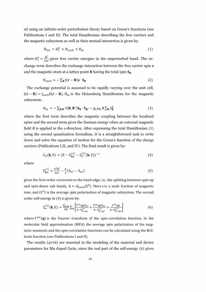
ed using an infinite-order perturbation theory based on Green’s functions (see
Publications I and II). The total Hamiltonian describing the free carriers and
the magnetic subsystem as well as their mutual interaction is given by:
H��� = H� + H�� + H� (1)
where H� = ��
��� gives free carrier energies in the unperturbed band. The ex-
change term describes the exchange interaction between the free carrier spin !and the magnetic atom at a lattice point " having the total spin #"
H�� = $ % J(& $ ")! ' #"" (2)
The exchange potential is assumed to be rapidly varying over the unit cell,
J(& $ ") = J���(& $ "), H� is the Heisenberg Hamiltonian for the magnetic
subsystem :
H� = $ % I(", ".)#"","3 ' #"3 $ g4�6 B % S"�
" (3)
where the first term describes the magnetic coupling between the localized
spins and the second term gives the Zeeman energy when an external magnetic
field B is applied in the z-direction. After expressing the total Hamiltonian (1)using the second quantization formalism, it is a straightforward task to write
down and solve the equation of motion for the Green’s function of the charge
carriers (Publications I,II, and IV). The final result is given by:
G8(9, E) = (E $ E98(:) $ ;8
(�)(9, E))<: (4)
where
E98(:) = ?�9�
��� $ @�
(�8� $ �8�) (5)
gives the first-order correction to the band edge, i.e., the splitting between spin-up
and spin-down sub bands, M = xJ���S��. Here x is a mole fraction of magnetic ions, and �OP� is the average spin polarization of magnetic subsystem. The second order self-energy in (4) is given by:
;8(�)(9, E) = UWXYZ
�
[\% ]^XX(_)`{�
|<|9}_,�(~) + ^��(_)`{�
|<|9}_,�(~) + ^��(_)
|<|9}_,{(~) �� (6)
where ���(_) is the Fourier transform of the spin-correlation function. In the molecular field approximation (MFA) the average spin polarization of the mag-netic moments and the spin-correlation functions can be calculated using the Bril-louin function (see Publications I and II).
The results (4)-(6) are essential in the modeling of the material and device
parameters for Mn doped GaAs, since the real part of the self-energy (6) gives

25
the higher order correction to the band energies, and its imaginary part gives
an estimate for the relaxation time of the charge carries in the case of the spin-
disorder scattering (see below).
The band splitting can be calculated self-consistently from Eqs. (4)-(6) by de-
termining the poles of the Green’s function (4) using numerical iterations as a
function of temperature in various magnetic fields. In the case of GaMnAs we
have used the following parameters:S = 5/2, a� = 5.���, the exchange integral
for the holes J��� = 1.4eV, and the exchange integral for the electrons J��
� =
0.2eV28,29. Curie temperature T is proportional to x, i.e., the fraction of mag-
netically active Mn ions, and can be estimated from the measured resistivity,
Hall effect (see Publication IV), or it can be taken from literature 42.
Figure 5. Temperature dependence of the valence band edge in GaMnAs at B=0 (solid curves) and B=4T (dashed curves) showing the band splitting at Tc =110K: a) the first order result, b) the higher order result. Reprinted with per-mission from N. Lebedeva and P. Kuivalainen, Journal of Applied Physics, vol. 93, pp. 9845-9864, 2003. Copyright 2003, Americal Institute of Physics.
Figure 5 shows the calculated temperature dependence of the valence band
edge in GaMnAs as a function of temperature at two values of the magnetic
field B. Higher-order corrections result in a 100 meV blue shift of the valence
band edge already in the paramagnetic region T> Tc. This shift has been ob-
served experimentally in a Gd-doped ferromagnetic semiconductor EuO (n-
type)47 as a red shift of the optical absorption edge, but not in the GaMnAs,
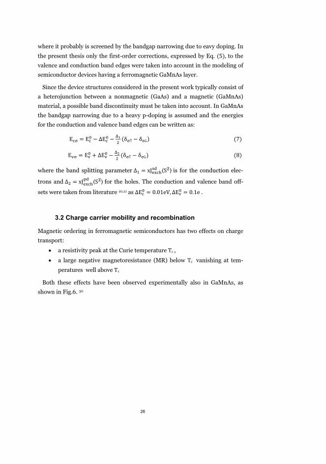
26
where it probably is screened by the bandgap narrowing due to eavy doping. In
the present thesis only the first-order corrections, expressed by Eq. (5), to the
valence and conduction band edges were taken into account in the modeling of
semiconductor devices having a ferromagnetic GaMnAs layer.
Since the device structures considered in the present work typically consist of
a heterojunction between a nonmagnetic (GaAs) and a magnetic (GaMnAs)
material, a possible band discontinuity must be taken into account. In GaMnAs
the bandgap narrowing due to a heavy p-doping is assumed and the energies
for the conduction and valence band edges can be written as:
E8 = E� $ ME
� $ @~�
(�8� $ �8�) (7)
E�8 = E�� + ME�
� $ @��
(�8� $ �8�) (8)
where the band splitting parameter M: = xJ��� �S�� is for the conduction elec-
trons and M� = xJ��� �S�� for the holes. The conduction and valence band off-
sets were taken from literature 10,11 as ME� = 0.01eV, ME�
� = 0.1e .
3.2 Charge carrier mobility and recombination
Magnetic ordering in ferromagnetic semiconductors has two effects on charge
transport:
� a resistivity peak at the Curie temperature Tc ,
� a large negative magnetoresistance (MR) below Tc vanishing at tem-
peratures well above Tc
Both these effects have been observed experimentally also in GaMnAs, as
shown in Fig.6. 30

27
a) b)
Figure 6. (a) Resistivity versus temperature for GaMnAs layers with differ-ent Mn content, arrows point to Curie temperature. Samples A0 and A1 are de-generate (metallic), B0 and A2 non-degenerate, though ferromagnetic, samples B1,B2 and A3 contain too little Mn for the onset of ferromagnetism. b) Resistivi-ty versus magnetic f ield at T< Tc for ferromagnetic GaMnAs layer. Reprintedwith permission from A. Van Esch, L. Van Bockstal, J De Boeck et al Phys.Rev.B 56 , 13103-13112 (1997) . Copyright 1997, American Institute of Physics. We have obtained similar results (see below and Publication IV).
The resistivity peak and the large magnetoresistance can be explained as a
contribution of the spin disorder scattering to the total mobility in ferromag-
netic semiconductors. In order to evaluate this effect the abovementioned
Green’s function technique can be applied. An estimate for the relaxation time
of the charge carriers ���8 �k��� can be obtained from the imaginary part of the
self-energy(6):
:���
{ (9)= �
?�Im;8
(�)(9)� = ��?
�UWXYZ�
[\� % ��(_)��E98 $ E9<_,���8� +_
���(_)��E98 $ E9<_,���8� + �(_)�(E98 $ E9<_,8)� (9)
In the degenerate semiconductor the charge carrier mobility can be estimated
using Eq.(9) and the following simple expression:
� = ��(9 )�� (10)
In the non-degenerated case �(k¡) should be replaced by
��� = ¢ |£/��}(¤}¤ )/¥¦§�(|) |¨©
¢ |£/��}(¤}¤ )/¥¦§ |¨©
(11)
Finally, in the presence of impurity scattering the total mobility can be calcu-
lated according to Mathiessen’s rule, which can be written as:
:ª«¬«
{ = :ª®¯
+ :ª��
{ (12)

28
In order to explain the temperature dependence of resistivity in the whole
temperature range 0-300 K and also in the case of low Mn concentration, a
conduction mechanism related to the impurity states shown in Fig.2 must be
added to the above resistivity model. This can be done with a Dubson-Holcomb
(DH)-model 48 for resistivity in heavily doped semiconductors. In this model
the temperature dependence of the resistivity is given by:
��°(T) = �±��² �±��²³
� ´ln µ1 + exp �|®<| ¶¦³
�·¸<:
(13)
where Em is the mobility edge in a disordered semiconductor.
Figure 7 shows the mobility vs. temperature in GaMnAs as calculated using
Eqs. (9) and (10). The calculated hole mobility vs. temperature and magnetic
field explains both the resistivity peak at the Curie temperature and negative
magnetoresistance for T < Tc (a detailed comparison of the resistivity model to
the experimental results is done in Figure 11 in Ch. 4.1.2 below).
Figure 7 . Hole mobility vs. temperature for spin-up and spin-down carriers at B=0T (solid curves) and B=4T (dashed curves) in GaMnAs in the case of spin disorder scattering. The material parameters are the same as in Figure 5. Re-printed with permission from N. Lebedeva and P. Kuivalainen, Journal of Ap-plied Physics, vol. 93, pp. 9845-9864, 2003. Copyright 2003, Americal Institute of Physics.
The mobility is an important model parameter also in semiconductor devices,
where the operation is based on charge carrier diffusion, such as pn-junctions
and bipolar transistors. This is due to the fact that the diffusion coefficient of
the charge carriers is proportional to the total mobility. In addition, in the pn-
junctions and bipolar transistors minority carrier recombination plays an
important role. The effects of the exchange interaction and band spiltting on

29
the recombination processes in a magnetic semiconductor have been discussed
in Publication II. The model predicts, e.g., a strong magnetic field dependence
for the recombination times, as shown in Figure 8. However, so far there is no
experimental evidence for the spin dependence of the recombination processes
in GaMnAs. This is due to the heavy doping concentration needed in the
ferromagnetic samples, which strongly decreases the minority carrier life-time
in Mn doped GaAs making it difficult to measure.
a) b)
Figure 8 . Direct band-to-band recombination time vs. temperature and mag-netic field in a) non-degenerate GaMnAs and b) degenerate GaMnAs. Reprinted with permission from N. Lebedeva and P. Kuivalainen, Journal of Applied Phys-ics, vol. 93, pp. 9845-9864, 2003. Copyright 2003, Americal Institute of Physics.

30
4 Semiconductor devices with a GaMnAs layer: theoretical modeling vs. experiments
4.1 Schottky diode
4.1.1 Modeling
The most simple semiconductor device is a Schottky diode consisting of a junc-
tion between a metal and a semiconductor. Since the current through the
Schottky diode depends exponentially on the height of the potential barrier
between the semiconductor and the metal, which in turn depends on the ener-
gy difference between the metal work function and the semiconductor band
edge, the band splitting due to ferromagnetic ordering in a magnetic semicon-
ductor should strongly affect the I-V curves of the diode. Thus, in principle, the
ferromagnetic Schottky diode can be used as a sensitive magnetic field sensor.
More generally, since the contact between the metal and the ferromagnetic
semiconductor exists in all spintronic devices, the modeling of its characteris-
tics as a function of temperature and magnetic field is a necessary task in the
design of all spintronic semiconductor devices.
For simplicity we can start the modeling with a textbook example of a junc-
tion between an n-type magnetic semiconductor, such as Eu-chalcogenides,
and a nonmagnetic metal having the work function larger than the electron
affinity of the semiconductor. In the case of the junction between a p-type
GaMnAs and the metal the band diagram should be just inverted.
Figure 9 . Energy band diagram for a ferromagnetic Schottky diode: (a) the ferromagnetic region extends into the depletion region having the width d, and (b) ferromagnetism is carrier induced, so that the magnetic layer extends only slightly into the depletion region. Reprinted with permission from H. Holmberg, G. Du, N. Lebedeva, S. Novikov, P. Kuivalainen, and X. Han, Journal of Physics: Conference Series, vol. 100, p. 052075, 2008. Copyright 2008, IOP Publishing Ltd.
31
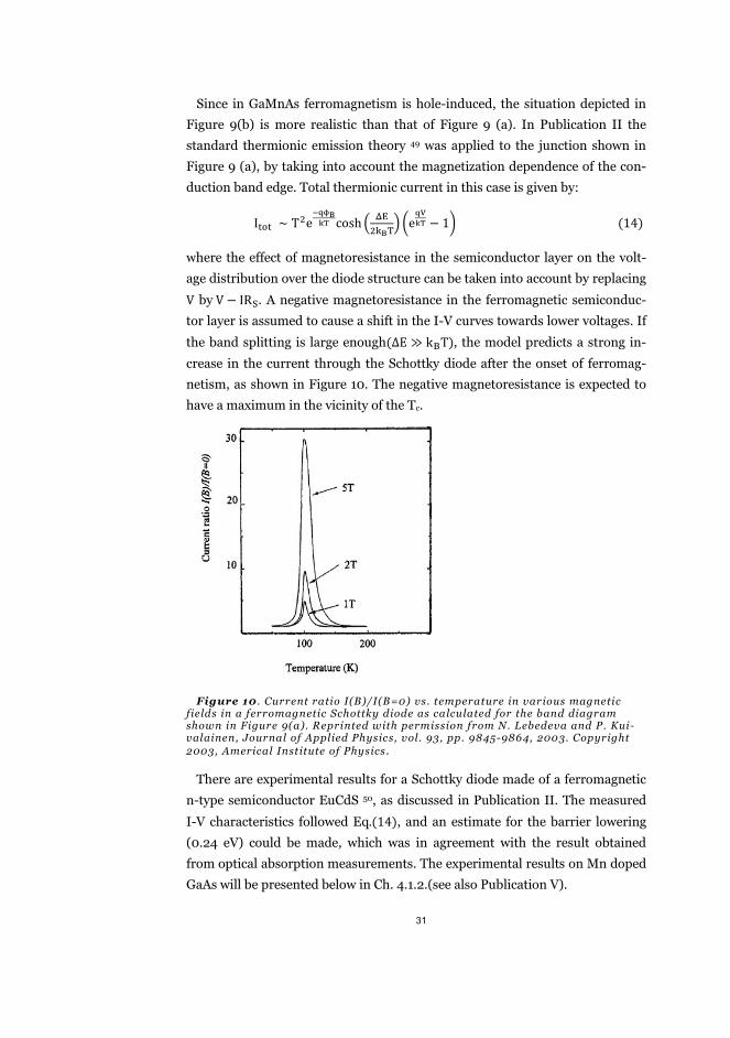
Since in GaMnAs ferromagnetism is hole-induced, the situation depicted in
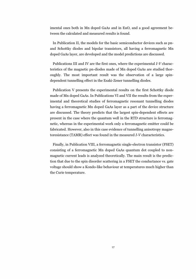
Figure 9(b) is more realistic than that of Figure 9 (a). In Publication II the
standard thermionic emission theory 49 was applied to the junction shown in
Figure 9 (a), by taking into account the magnetization dependence of the con-
duction band edge. Total thermionic current in this case is given by:
I��� º T�e}»¼¦
¥§ cosh � @|�¶¦³
� ½e»¾¥§ $ 1¿ (14)
where the effect of magnetoresistance in the semiconductor layer on the volt-
age distribution over the diode structure can be taken into account by replacing
V by V $ IR�. A negative magnetoresistance in the ferromagnetic semiconduc-
tor layer is assumed to cause a shift in the I-V curves towards lower voltages. If
the band splitting is large enough(ME À k6T), the model predicts a strong in-
crease in the current through the Schottky diode after the onset of ferromag-
netism, as shown in Figure 10. The negative magnetoresistance is expected to
have a maximum in the vicinity of the Tc.
Figure 10 . Current ratio I(B)/I(B=0) vs. temperature in various magnetic fields in a ferromagnetic Schottky diode as calculated for the band diagram shown in Figure 9(a). Reprinted with permission from N. Lebedeva and P. Kui-valainen, Journal of Applied Physics, vol. 93, pp. 9845-9864, 2003. Copyright 2003, Americal Institute of Physics.
There are experimental results for a Schottky diode made of a ferromagnetic
n-type semiconductor EuCdS 50, as discussed in Publication II. The measured
I-V characteristics followed Eq.(14), and an estimate for the barrier lowering
(0.24 eV) could be made, which was in agreement with the result obtained
from optical absorption measurements. The experimental results on Mn doped
GaAs will be presented below in Ch. 4.1.2.(see also Publication V).

32
In the case of Figure 9(b) the thermionic component of the current remains
unchanged under the onset of the band splitting. However, the tunnelling cur-
rent increases due to a shortening of the barrier by M d. Since the tunnelling
current depends exponentially on the barrier height qÁ6 and the width d, the
relative change of the tunnelling current due to band splitting can be written as
MI/I º exp ( MdÂ����æ?� ) $ 1 (15)
where the shortening of the barrier can be estimated to be@
Ä ME/qÁ6. Also in
this case a negative magnetoresistance is expected in the Schottky diode,
which, however, is much smaller than in the previous case.
4.1.2 Experimental result on Pt/GaMnAs Schottky diode
Various GaMnAs thin films with Mn mole fraction x varying from 0.02 to 0.05
were grown in our VG100H MBE system at Aalto University. All films were
grown on semi-insulating GaAs (100) substrates. First, the surface was chemi-
cally cleaned and possible oxide was removed. After that a buffer layer of un-
doped GaAs was grown at 5800C. Then the growth temperature was decreased
to 2300C and a 1μm thick Mn doped GaAs layer was grown. During the growth
process the crystalline quality of the film was controlled using a Reflection
High Energy Electron Diffraction (RHEED)-technique. The Mn doped GaAs
films were first characterized by measuring the resistivity vs. temperature. The
ohmic contacts Pt/Ni/Pt/Au to the p+ layer were deposited by an e-beam vac-
uum evaporation technique and resistivity was measured in the Van-der-Pauw
configuration. The hole concentration was evaluated at the room temperature
through Hall measurements. The behavior of the resistivity curve changes from
insulating to metallic while the hole concentration increases, as shown in Fig-
ure 11. These results are very similar to those obtained by another research
group (see Figure 6 above). The onset of ferromagnetism is manifested by the
appearance of a local maximum at Tc on the ���� curve. Negative magnetore-
sistance is seen in both magnetic field polarities, being most prominent at the
Curie temperature (Figure 11b). The solid curves in Figure 11a have been calcu-
lated by combining the spin disorder scattering model, Eq.(9), with the Dub-
son-Holcomb-model, Eq.(13). The agreement between the theoretical and ex-
perimental results is excellent.

33
Figure 11. a) Resistivity vs. temperature in GaMnAs films with room temper-ature hole concentrations 5.6 101 9 ,7.0 1019 and 1.7 102 0 cm- 3(from top to bot-tom); the inset shows the lowest curve in more detail. The solid curves have been calculated by combining the spin disorder scattering model, Eq. (7), with a Dub-son-Holcomb model, Eq.(11). b) Magnetoresistance [�(B)- �(0)]/ �(0) vs. mag-netic field at various temperatures in GaMnAs with x=0.04 (p=1.7 1020 ). Re-printed with permission from H. Holmberg, N. Lebedeva, S. Novikov, P. Kuiva-lainen, M. Malfait, and V. V. Moshchalkov, Physica Status Solidi (a), vol. 204, pp.791-804, 2007. Copyright 2007, WILEY-VCH Verlag.
The ferromagnetic behavior of our GaMnAs samples with Curie temperatures
varying from 30 to 70K was verified by direct magnetization measurements, an
example is shown in Figure 12.
Figure 12. Magnetic moment vs. temperature in a GaMnAs film measured by using a vibrating sample magnetometer at B=10mT. The inset shows the mag-netic hysteresis measured at 10K. Reprinted with permission from H. Holmberg, N. Lebedeva, S. Novikov, P. Kuivalainen, M. Malfait, and V. V. Moshchalkov, Physica Status Solidi (a), vol. 204, pp.791-804, 2007. Copyright 2007, WILEY-VCH Verlag.
34
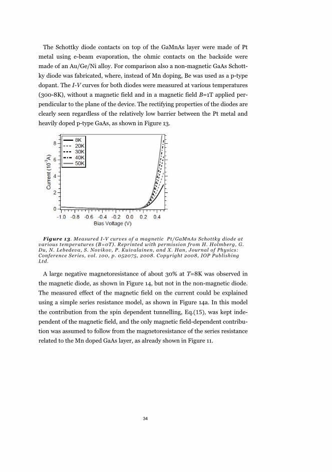
The Schottky diode contacts on top of the GaMnAs layer were made of Pt
metal using e-beam evaporation, the ohmic contacts on the backside were
made of an Au/Ge/Ni alloy. For comparison also a non-magnetic GaAs Schott-
ky diode was fabricated, where, instead of Mn doping, Be was used as a p-type
dopant. The I-V curves for both diodes were measured at various temperatures
(300-8K), without a magnetic field and in a magnetic field B=1T applied per-
pendicular to the plane of the device. The rectifying properties of the diodes are
clearly seen regardless of the relatively low barrier between the Pt metal and
heavily doped p-type GaAs, as shown in Figure 13.
Figure 13 . Measured I-V curves of a magnetic Pt/GaMnAs Schottky diode at various temperatures (B=0T). Reprinted with permission from H. Holmberg, G. Du, N. Lebedeva, S. Novikov, P. Kuivalainen, and X. Han, Journal of Physics: Conference Series, vol. 100, p. 052075, 2008. Copyright 2008, IOP Publishing Ltd.
A large negative magnetoresistance of about 30% at T=8K was observed in
the magnetic diode, as shown in Figure 14, but not in the non-magnetic diode.
The measured effect of the magnetic field on the current could be explained
using a simple series resistance model, as shown in Figure 14a. In this model
the contribution from the spin dependent tunnelling, Eq.(15), was kept inde-
pendent of the magnetic field, and the only magnetic field-dependent contribu-
tion was assumed to follow from the magnetoresistance of the series resistance
related to the Mn doped GaAs layer, as already shown in Figure 11.

35
a) b)
Figure 14 . a) Effect of the external magnetic field on the I-V curves of the magnetic Schottky diode at T=8K, dots show fitted curves calculated using aseries resistance model. b) Magnetoresistance vs. bias voltage at T=8K. Re-printed with permission from H. Holmberg, G. Du, N. Lebedeva, S. Novikov, P. Kuivalainen, and X. Han, Journal of Physics: Conference Series, vol. 100, p. 052075, 2008. Copyright 2008, IOP Publishing Ltd.
The only manifestation of the magnetization dependent tunnelling current
may be the anomalous voltage dependent MR shown in Fig. 14b at low voltag-
es. This effect may be related to a change from a tunnelling current dominating
MR at low voltages to the series resistance dominated MR at higher voltages.
However, this question remains open to some extent.
4.1.3 Conclusions
It is very straightforward to model the special properties of magnetic Schottky
diodes by starting with the conventional thermionic emission theory and then
adding the magnetization dependent effects by considering the band splitting
and the consequent Schottky barrier lowering, and the magnetoresistance of
the series resistance of the magnetic semiconductor layer. Our experimental
results on Pt/GaMnAs Schottky diodes indicate the situation where the mag-
netic field-dependence of the series resistance masks the possible spin-
dependent tunnelling contributions in the I-V characteristics.
Mn doped GaAs is not an optimal material for large magnetoresistance ef-
fects, since it is always of p-type leading to small Schottky barriers, and its Cu-
rie temperature is low allowing the appearance of significant MR effects only at
low temperatures. A better candidate for sensitive magnetic field sensors would
be, e.g., Mn doped GaN, which in addition to having a high Tc also has been
reported to be of n-type. 51
36
4.2 P-N diode
4.2.1 Modeling
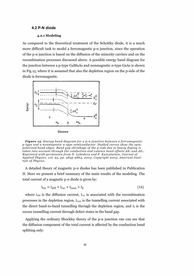
As compared to the theoretical treatment of the Schottky diode, it is a much
more difficult task to model a ferromagnetic p-n junction, since the operation
of the p-n junction is based on the diffusion of the minority carriers and on the
recombination processes discussed above. A possible energy band diagram for
the junction between a p-type GaMnAs and nonmagnetic n-type GaAs is shown
in Fig.15, where it is assumed that also the depletion region on the p-side of the
diode is ferromagnetic.
Figure 15. Energy band diagram for a p-n junction between a ferromagnetic p-type and a nonmagnetic n-type semiconductor. Dashed curves show the spin-polarized band edges. Band gap shrinkage of the p-side due to heavy doping is ����������������� ��� �� ������������������������������������c ������v.Reprinted with permission from N. Lebedeva and P. Kuivalainen, Journal of Applied Physics, vol. 93, pp. 9845-9864, 2003. Copyright 2003, Americal Insti-tute of Physics.
A detailed theory of magnetic p-n diodes has been published in Publication
II. Here we present a brief summary of the main results of the modeling. The
total current of a magnetic p-n diode is given by:
I��� = I ÅÆÆ + IÇ� + I�ÈÉÉ + IÊ (16)
where Idiff is the diffusion current, Irec is associated with the recombination
processes in the depletion region, Itunn is the tunnelling current associated with
the direct band-to-band tunnelling through the depletion region, and IX is the
excess tunnelling current through defect states in the band gap.
Applying the ordinary Shockley theory of the p-n junction one can see that
the diffusion component of the total current is affected by the conduction band
splitting only:

37
I ÅÆÆÌ = AqnÅ� ]�Í��
Î~�¥§ÏΤY
©/¥§
�4Í�\Ð+ �Í��
Î~�¥§ÏΤY
©/¥§
�4Í�\Ð+ �¯�}Τѩ/�¥§
4¯\�� �e(�Ò<ÓÔ�)/¶³ $ 1� (17)
where A is the area of the diode, ni is the intrinsic carrier concentration,
D�(�)�D�� is the carrier diffusion coefficient for the electrons (holes), L�(�)(L�)
is the diffusion length of the electrons (holes), and NA(ND) is the acceptor (do-
nor) concentration, RS is the series resistance of the diode. In the nonmagnetic
case M: = 0 and in the absence of the band discontinuities Eq.(17) reduces to
the standard Shockley equation for a p-n junction. 49
The magnetic part (the first two terms in Eq.(17)) will contribute significantly
to the total current if the following condition is fulfilled:
N� Õ NÖÂ�Í�¯
�¯�Íe<(@|Y
©×@|Ñ©)/¶³ (18)
In a GaMnAs p+n junction NÖ À N�, but the large band discontinuity in the
valence band may help to reach the condition (18), and then a significant mag-
netoresistance effect is possible near the Curie temperature in the case depict-
ed in Figure 15. Figure 16 shows the diffusion current vs. temperature in vari-
ous magnetic fields as calculated from Eq.(17). The rather small magnetore-
sistance at low fields is due to the small value of the band splitting parameter
�1 in the conduction band of GaMnAs.
Figure 16 . Calculated diffusion current ratio I(B)/I(0) vs. temperature in various magnetic f ields in an ideal ferromagnetic p-n junction. The results have been calculated from Eq.(17���� ��1=0.025eV ���2=0.1 eV, NA/ND=10, and TC=100 K. Reprinted with permission from N. Lebedeva and P. Kuivalainen, Journal of Applied Physics, vol. 93, pp. 9845-9864, 2003. Copyright 2003, Americal Institute of Physics.

38
In Publication II we have shown that under favorable conditions, e.g., in
magnetic p-n junctions with nondegenerate p- and n-regions, the magnetore-
sistance due to the recombination current may be even larger than the one re-
lated to the diffusion current. However, in GaMnAs p-n diodes the magnetic
side is always heavily doped, which significantly reduces the MR effect, as dis-
cussed below.
4.2.2 Experimental results for GaMnAs p-n diodes with a lightly doped n-region
After the fabrication process for the ferromagnetic GaMnAs thin films was op-
timized, we started to fabricate p-n diodes having a GaMnAs layer as the p-
side. The structure of the diode is presented in Figure 17. The doping concen-
tration of the n-type substrate was 1017cm-3, on top of which a 250 nm thick Si-
doped GaAs film was grown (n=1017cm-3). Above the n-layer a 0.5μm thick
GaMnAs p-layer was grown. Pt/Ni/Pt/Au and Au/Ge/Ni/Au ohmic contacts
were evaporated on the front and back sides, respectively.
Figure 17 . Schematic structure of the magnetic p–GaMnAs/n-GaAs diode. Re-printed with permission from H. Holmberg, N. Lebedeva, S. Novikov, P. Kuiva-lainen, M. Malfait, and V. V. Moshchalkov, Physica Status Solidi (a), vol. 204, pp.791-804, 2007. Copyright 2007, WILEY-VCH Verlag.
The I-V characteristics of the p-n diode were measured in the wide tempera-
ture range (10-300K), with and without a magnetic field perpendicular to the
plane of the device (B=� 1T). The strong T-dependence of the I-V curves van-
ishes at T<100K, as shown in Figure 18. This behavior, which is similar to one
reported by Arata et al. 11, can be attributed to the valence band offset between
GaMnAs and GaAs: at low temperatures the T-dependent diffusion current
becomes negligible and conduction is dominated by the T-independent excess
current Ix mentioned in Eq.(16). No magnetoresistance effect was found in
these diodes at any temperature.

39
Figure 18 . Measured I-V characteristics at various temperatures in a p+nGaMnAs/GaAs diode with a lightly doped (ND=1017 cm- 3) non-magnetic side.Reprinted with permission from H. Holmberg, N. Lebedeva, S. Novikov, P. Kui-valainen, M. Malfait, and V. V. Moshchalkov, Physica Status Solidi (a), vol. 204, pp.791-804, 2007. Copyright 2007, WILEY-VCH Verlag.
The absence of the magnetoresistance effect in the GaMnAs/GaAs pn-
junction having a lightly-doped nonmagnetic region could be due to several
reasons:
i. Since ND<<NA, the lightly doped nonmagnetic side of the junction dom-
inates the diffusion current and therefore total current does not depend
on the band splitting. Also, due to the high doping of the p-side, neces-
sary for onset of ferromagnetism, the condition for the dominance of
the magnetic part of the recombination current is not fulfilled.
ii. The conduction band splitting parameter �1 can be as small as the
thermal energy leading to an unsubstantial band splitting and MR ef-
fect.
iii. There is no ferromagnetic ordering in the depletion region of the diode
due to the absence of free holes. Therefore the magnetic field does not
change the built in potential of the diode, in contrast to the predictions
of the model above, which are used as the starting point the situation
depicted in Figure 15.
iv. The excess current, which does not depend on the magnetic field, dom-
inates at low temperatures.
40
4.2.3 Conclusions
We think that the absence of ferromagnetism in the depletion region of the
magnetic GaMnAs/GaAs diode is the most probable reason for not observing
any MR effect, not even at low temperatures. Actually, the expectations were
not very high for this type p-n diode, since it is well known 49 that the dc cur-
rent in the p-ndiodes is always dominated by the more lightly doped side of the
diode, which in the case of Figure 15 was nonmagnetic. The situation is quite
different in the case where both sides of the magnetic diode are heavily doped,
as discussed in Ch.4.3 below.
4.3 Ferromagnetic Esaki-Zener Tunnelling diode
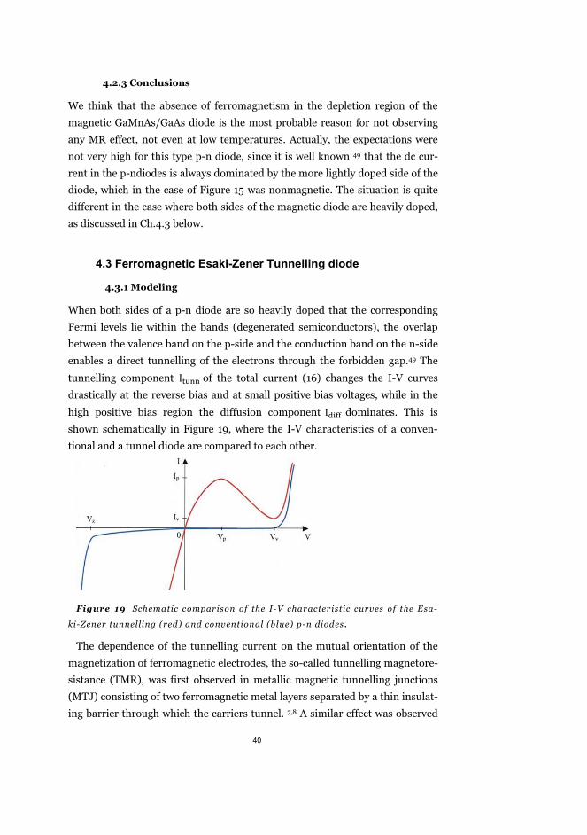
4.3.1 Modeling
When both sides of a p-n diode are so heavily doped that the corresponding
Fermi levels lie within the bands (degenerated semiconductors), the overlap
between the valence band on the p-side and the conduction band on the n-side
enables a direct tunnelling of the electrons through the forbidden gap.49 The
tunnelling component I�ÈÉÉ of the total current (16) changes the I-V curves
drastically at the reverse bias and at small positive bias voltages, while in the
high positive bias region the diffusion component I ÅÆÆ dominates. This is
shown schematically in Figure 19, where the I-V characteristics of a conven-
tional and a tunnel diode are compared to each other.
Figure 19 . Schematic comparison of the I-V characteristic curves of the Esa-
ki-Zener tunnelling (red) and conventional (blue) p-n diodes.
The dependence of the tunnelling current on the mutual orientation of the
magnetization of ferromagnetic electrodes, the so-called tunnelling magnetore-
sistance (TMR), was first observed in metallic magnetic tunnelling junctions
(MTJ) consisting of two ferromagnetic metal layers separated by a thin insulat-
ing barrier through which the carriers tunnel. 7,8 A similar effect was observed

41
in structures with ferromagnetic GaMnAs layers instead of metal layers. 52,53,54
Moreover, in the all-semiconductor MTJs the TMR effect is sensitive to the
direction of the applied magnetic field with respect to the direction of current
and crystallographic axis. This so-called tunnelling anisotropic magnetore-
sistance (TAMR) effect was observed in structures containing a single ferro-
magnetic electrode 55,56, as well as in typical MTJs with two ferromagnetic con-
tacts 57,58.
In the case of the tunnelling diode, where the p-side is a heavily doped ferro-
magnetic GaMnAs layer, and the n-side is a heavily doped nonmagnetic GaAs
layer, it is natural to assume that the tunnelling term I�ÈÉÉ of the total current
(16) becomes dependent on the magnetic ordering (and hence on temperature
and magnetic field) due to the effect of band splitting on the density of states
and due to the spin dependence of the tunnelling probability. The band dia-
gram of the magnetic tunnel diode is shown in Figure 20.
Figure 20 . Schematic energy diagram for a tunnel diode, where the p-side is ferromagnetic. The dashed lines show the spin-polarized band edges. EF p and EF n are the quasi-Fermi levels for holes and electrons, and V is the applied volt-age. It is assumed that there is no band splitting (ferromagnetism) in the deple-tion region. Reprinted with permission from H. Holmberg, N. Lebedeva, S. Novikov, P. Kuivalainen, M. Malfait, and V. V. Moshchalkov, Physica Status Solidi (a), vol. 204, pp.791-804, 2007. Copyright 2007, WILEY-VCH Verlag.
The effect of the ferromagnetic ordering and the consequent changes in the
density of states (DOS) in the valence band in a GaMnAs/GaAs tunnelling di-
ode can be estimated using the standard expression for the direct inter-band
tunnelling current:
I�ÈÉÉ = AC % ¢ T8(E)[f(E) $ f�8(E)]|�(�)
|(É)8 D(E)D�8(E)dE (19)

42
where A is the area of the diode, C is a constant that does not depend on tem-
perature nor on the magnetic field, ÚÛ and ÚÜÝ are the densities of states for
conduction and valence bands, respectively, which are given by:
DÞ(E) = ßà��£/�á���?£ (E $ EÞ)�~ (20)
DÒ8(E) = :
��Z
�£/�á���?£ �EÒ $ E $ @�
�(�8� $ �8�)�
�� (21)
The parameters p1 and p2 have the value ½ in the case of parabolic bands.
However, in heavily doped disordered semiconductors with tail states at ener-
gies close to the band edges these parameters can have values larger than ½.
According to the calculations presented in Publication IV, the change in tunnel-
ling probability T8(E) due to the valence band splitting causes only negligible
(<0,1%) changes in the tunnelling current. On the other hand, the changes in
the density of states due to the band splitting can cause a sizable decrease
(-5%) in the tunnelling current in the case of parabolic bands, as shown in Fig-
ure 21, where the results were calculated from Eqs.(19)-(21). This decrease in
the tunnelling component of the total current through the ferromagnetic Ze-
ner-Esaki diode and its dependence on temperature and magnetic field should
follow the corresponding dependences of the magnetization in the GaMnAs
layer.
Figure 21. Calculated tunnelling current vs voltage for the tunnel diode with ferromagnetic p-side in the case of parabolic bands (p=1/2). Solid curves corre-spond to the case with no band splitting, the dashed and dotted curves – to �2������������2=0,2eV. Reprinted with permission from H. Holmberg, N. Leb-edeva, S. Novikov, P. Kuivalainen, M. Malfait, and V. V. Moshchalkov, Physica Status Solidi (a), vol. 204, pp.791-804, 2007. Copyright 2007, WILEY-VCH Ver-lag.
In the calculations above the mutual orientation of the applied magnetic field
and the direction of tunnelling current were not taken into account. Indeed, a
more accurate model for the magnetization dependence of the tunnelling cur-

43
rent can be developed by taking into account not only the band splitting but
also the anisotropy of the density states, i.e., its dependence on the orientation
of the magnetization. The theory of anisotropic tunnelling magnetoresistance
(TAMR) has been developed by several authors59,60. Its basic idea is the follow-
ing: due to the exchange interaction there is a strong anisotropy in the Fermi
surface of GaMnAs, related to the direction of magnetization, which in turn
causes uniaxial anisotropic changes in the density of states (DOS) in the va-
lence band of GaMnAs. Consequently, a rotation of the magnetization with re-
spect to the direction of the tunnelling current by an applied magnetic field
causes a change in the DOS, and according to Eq.(19), in the tunnelling cur-
rent. The models 59,60 predict an in-plane TAMR effect in the GaMnAs/GaAs
Esaki-Zener tunnelling diodes, the magnitude of which should be in the order
of several percents at moderate magnetic fields. The spin-dependent interband
tunnelling is also sensitive to the rotation of magnetization achived by applying
an out-of-plane magnetic field. The magnitude of perpendicular TAMR is de-
fined as:
TAMRâ =R(Hâ) $ R(0)
R(0)
where ã(äâ) and ã(0) are the resistances in the cases of the out-of-plane and
in-plane saturated magnetization, respectively. Since in the ferromagnetic
GaMnAs thin films the easy axis of the magnetization lies in the plane of the
film, the transverse TAMR can be observed at the temperatures lower than the
Curie temperature under the application of a perpendicular-to-plane magnetic
field, if it is strong enough to rotate the magnetization from the in-plane direc-
tion to the out-of-plane direction.
4.3.2 Experimental results for the spin Esaki-Zener tunnelling di-ode
The first experimental results for the ferromagnetic GaMnAs/GaAs tunnelling
diode were published in Publication III and later in more detail in Publication
IV. When during the growth of the p-n diode also the n-side was heavily doped
(1019 cm-3), we obtained the device in which the I-V curves exhibited typical
features of the tunnelling diode. As shown in Figure 22, in the voltage range
0.2-0.4V there is clearly seen a negative resistance region due to the inter-band
tunnelling. At low temperatures T< 100K the current becomes only weakly T-
dependent, in the same way as in the conventional p-n diodes discussed above.
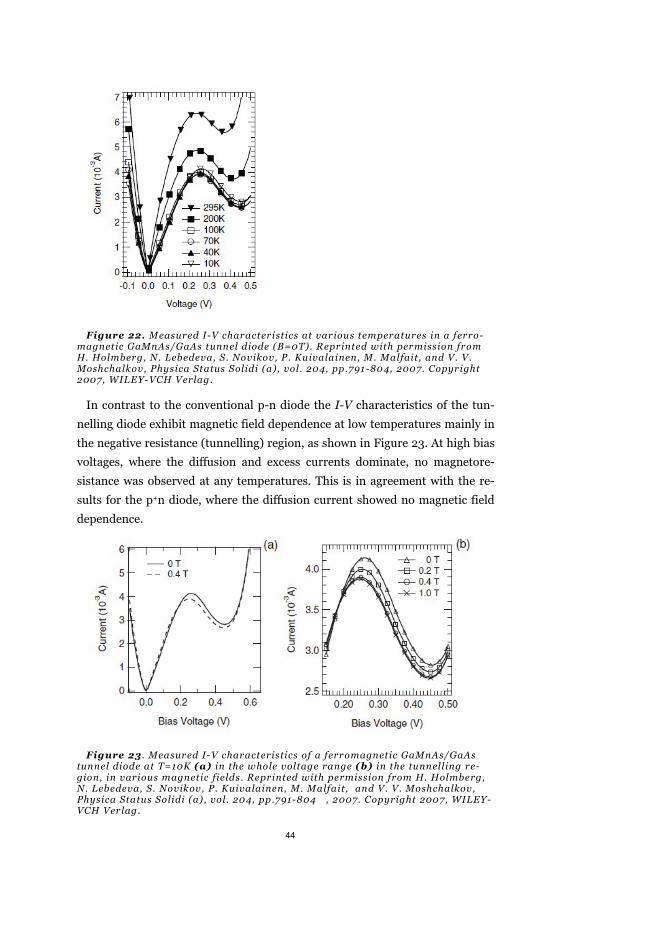
44
Figure 22. Measured I-V characteristics at various temperatures in a ferro-magnetic GaMnAs/GaAs tunnel diode (B=0T). Reprinted with permission from H. Holmberg, N. Lebedeva, S. Novikov, P. Kuivalainen, M. Malfait, and V. V. Moshchalkov, Physica Status Solidi (a), vol. 204, pp.791-804, 2007. Copyright 2007, WILEY-VCH Verlag.
In contrast to the conventional p-n diode the I-V characteristics of the tun-
nelling diode exhibit magnetic field dependence at low temperatures mainly in
the negative resistance (tunnelling) region, as shown in Figure 23. At high bias
voltages, where the diffusion and excess currents dominate, no magnetore-
sistance was observed at any temperatures. This is in agreement with the re-
sults for the p+n diode, where the diffusion current showed no magnetic field
dependence.
Figure 23. Measured I-V characteristics of a ferromagnetic GaMnAs/GaAs tunnel diode at T=10K (a) in the whole voltage range (b) in the tunnelling re-gion, in various magnetic fields. Reprinted with permission from H. Holmberg, N. Lebedeva, S. Novikov, P. Kuivalainen, M. Malfait, and V. V. Moshchalkov, Physica Status Solidi (a), vol. 204, pp.791-804 , 2007. Copyright 2007, WILEY-VCH Verlag.
45
The measured peak current decrease is in good agreement with that predict-
ed above for the tunnelling current in the case of the parabolic bands, and it
has the same order of magnitude (�I/I=8% ) as the value calculated from
Eq.(19) in the case of the valence band splitting parameter �2=0,2eV (�I/I=5%,
see Fig.21). As it is shown in Fig.24, the relative current change saturates in
higher magnetic fields, which again is in agreement with the theory, since
�I�ÈÉÉ/I�ÈÉÉ~�D�/D�~���~�Sæ��, and �Oç� saturates with increasing B.
Figure 24. Relative change of the tunnelling current (I(B)-I(0))/I(0) vs.magnetic f ield at various temperatures in a GaMnAs/GaAs tunnel diode near the peak voltage (V=300mV). Reprinted with permission from H. Holmberg, N. Leb-edeva, S. Novikov, P. Kuivalainen, M. Malfait, and V. V. Moshchalkov, Physica Status Solidi (a), vol. 204, pp.791-804, 2007. Copyright 2007, WILEY-VCH Ver-lag.
In small magnetic fields the above relation�Ó«èÍÍÓ«èÍÍ
~�D�/D�~���~�S�~B� pre-
dicts a parabolic B-dependence for the relative current change, which is also
observed in Fig.24 in the field range B=0-0.2T.
At low bias voltages V<0.2V the applied magnetic field increases the current
slightly. This effect could result from a shift of the I-V curves towards the lower
voltages due to the negative magnetoresistance of the GaMnAs layer on the
ferromagnetic p-side. However, since this shift is not observed at higher volt-
ages (V>0,5V), we have to state that its origin remains unexplained.
It is interesting to note that at the same time when we obtained the first re-
sults on the spin-dependent tunnelling published in Publication III, also an-
other independent research group 56 published very similar results. All our ob-

46
served effects of the magnetic field on the conductance of ferromagnetic Zener-
Esaki diode fit very well with published data on TMR in the similar device,
when magnetic field is switched from in-plane to out-of-plane direction 56 , as
shown in Figure 25.
a) b)
Figure 25. (a)Relative current change I(B)-I(0)/I(0) under the application of an out-of-plane magnetic field in the Zener-Esaki tunnelling diode, presented as a function of bias voltage at different temperatures (adopted from thePublica-tion IV). Reprinted with permission from H. Holmberg, N. Lebedeva, S. Novikov, P. Kuivalainen, M. Malfait, and V. V. Moshchalkov, Physica Status Solidi (a), vol. 204, pp.791-804, 2007. Copyright 2007, WILEY-VCH Verlag. (b) Magneto-resistance in a similar GaMnAs/GaAs tunnelling diode under the rotation of applied magnetic f ield from the in-plane to the out-of-plane direction, as a func-tion of bias voltage. Figure (b) is reprinted with the permission from R. Gi-raud,M. Gryglas, L. Thevenard, A. Lemaître, and G. Faini, Appl. Phys. Lett. 87(24), 242505,1-3 (2005). Copyright 2005, American Institute of Physics
Both the negative magnetoresistance (current increases under application of
magnetic field) at the low bias voltages and positive magnetoresistance for
larger positive bias (tunnelling region) are seen in the results published by both
groups. Therefore our results can also be related not only to the change in the
DOS due to the band splitting but more accurately to the tunnelling anisotropic
magnetoresistance (TAMR) effect due to the changes in the anisotropic DOS
caused by the changes in the direction of the magnetization.
4.3.3 Conclusions
We have observed spin-dependent tunnelling and a large (up to 20%) magne-
toresistance effect at low temperatures (10K) in the ferromagnetic
GaMnAs/GaAs Zener-Esaki tunnelling diode. The MR effect is related to the
spin dependence of the DOS in the ferromagnetic GaMnAs layer, or more accu-
rately to the anisotropy in the magnetization dependence of the DOS in the

47
valence band. Our experimental results are in good agreement with those ob-
tained independently by another research group. As shown in Figure 25, the
large MR is seen at very low bias voltages, which could allow low power
spintronic applications. Another application of the ferromagnetic tunnelling
diode could be related to the electrical injection of spin-polarized carriers in a
spin injector or a spin filter. The electrical spin injection from p-GaMnAs into a
nonmagnetic semiconductor was first achieved by injection of spin-polarized
holes (under positive bias in the tunnelling diode)61. Under the negative bias
the spin-polarized electrons tunnel from the valence band of GaMnAs into the
conduction band of the non-magnetic n-side62. Recently, a very high spin po-
larization of the injected current (80%) has been observed in such devices. 63,64
4.4 Magnetic resonant tunnelling diode
Resonant tunnelling is a quantum phenomena that can be briefly described as
follows: while the transmission probability for a particle incident on a rectan-
gular potential barrier is always less than one, a double barrier structure can be
completely transparent for particles with certain energies, namely those coin-
cident with quantized energy levels in the quantum well (QW), formed by the
potential barriers.
A resonant tunnelling diode (RTD) is a semiconductor device consisting of an
emitter (heavily doped, narrow-band gap material), a quantum well between
two barriers made of a large band gap material, and a collector, with electrical
contacts attached to the emitter and the collector, as shown in Figure 26a. At
certain values of the applied voltage the I-V characteristics of the RTD exhibit
peaks that correspond to the resonant tunnelling of the charge carriers from
the emitter through the quantized levels in the quantum well (HH1, LH1, HH2
for a GaAs QW) to the collector (at positive bias for the p-type device) or from
collector to the emitter (at negative bias).
48
a) b)
Figure 26. a) Schematic diagram of the valence band profile of the p-type GaAs/AlAs resonant tunnelling diode under an applied voltage V. b) I-V char-acteristic of the RTD. Reprint with the permission from Johnny Ling, University of Rochester.
The research of RTDs has been intensive for many decades. The effect of a
magnetic field on the I-V characteristics of the nonmagnetic GaAs/AlAs RTD
was studied for the first time by Mendez 65 and Hayden66. It was observed that
high magnetic field (B>2T) applied perpendicular to the junction causes the
appearance of additional maxima on the low-voltage side of the resonances due
to the Landau level formation inside the quantum well (QW) 66, while the field
applied parallel to the junction causes a shift of resonances due to the quantiza-
tion of the charge carrier motion in the plane of the QW 65. After the discovery
of the DMS materials the study of RTDs were extended to the RTD structures
having a ferromagnetic QW 69, emitter 67,68, or/and collector. In the RTD with a
ferromagnetic Mn-doped GaAs emitter, fabricated by Ohno et al. 67,68, a spon-
taneous spin splitting of the valence band was observed in the I-V characteris-
tics as splittings of the LH1 and HH2 resonant peaks, which appeared at T<Tc
and increased with the magnetic field in good agreement with the theory pre-
sented below.
4.4.1 Modeling of the RTD with a ferromagnetic emitter.
Modeling of non-magnetic RTDs is a mature field, but recently also magnetic
RTDs with a ferromagnetic emitter or a QW have been modeled by several
groups.70-73 The magnetic RTD with the ferromagnetic emitter is obtained from
the non-magnetic RTD shown in Figure 26a simply by doping heavily the up-
permost GaAs layer with Mn. In the case of a symmetrical quantum well and
under a positive bias the device acts as a RTD with a ferromagnetic emitter,
and under a negative bias it acts as a RTD with a ferromagnetic collector, as

49
shown in Figure 27. At temperatures below Tc spontaneous band splitting in
the magnetic layer is expected to change the I-V characteristics of the device.
These changes are expected to be more prominent for a hole injection from the
ferromagnetic emitter into the non-magnetic collector (positive bias), than for
a hole injection from the non-magnetic emitter into the ferromagnetic collector
(negative bias).
Figure 27 . Band diagram for RTD with a) a ferromagnetic emitter, and b)with a ferromagnetic collector, in both cases the band splitting is non-������!�"�Reprinted with permission from H. Holmberg, N. Lebedeva, S. Novikov, P. Kui-valainen, G. Du, X. Han, M. Malfait, and V. V. Moshchalkov, Physica Status Sol-idi (a), vol. 204, pp.3463-3477, 2007. Copyright 2007, WILEY-VCH Verlag.
A straightforward way to model a RTD with a ferromagnetic emitter is to
modify the well-known Tsu-Esaki formula74 for the tunnelling current by tak-
ing into account the band splitting �. Then the total current including the spin-
up and spin-down contributions is given by
I��� = I���� + I���
� = ¢ T�(E)S�(E)dEé� + ¢ T�(E)S�(E)dEé
@ (22)
where T8(E) is the quantum mechanical transmission coefficient through the
double barrier structure given by the following Lorenzian:
T8(E) = ^ê^ë
��
�×�|<|©
íWî�� (23)
Here � = �4 + �Ô is the spin-independent full width of the half-maximum of
the resonance. The partial widths �4 and �Ô for the left and right barriers, re-
spectively, can be calculated in a straightforward manner in the case of rectan-
gular barriers.75 In Eq.(22) the bottom of the spin-up subband was taken as a
zero energy level and the energy of the resonant level can be written as:

50
E8Ç�� = E� $ �Òïð
�+ @
� (�8� $ �8�) (24)
where ñ� is the energy of the single quantized level in the QW in the absence of
band splitting and the voltage over the double barrier structure Vòó is assumed
to be divided equally between the two barriers. The spin-dependent supply
function S8(E) in Eq.(22) is given by:
S8(E) = ����¶³[��?£ � ln ]:×�(¤ {
ê }¤)/¥§
:×�(¤ {ë }¤)/¥§
� (25)
The effect of the band splitting on the total current as calculated from Eq.(22)
is shown in Figure 28. Here we have added a magnetization-independent leak-
age current to the total current (Publication VI).
Figure 28. a) Calculated I-V characteristics of FRTD with ferromagnetic emitter (Tc=110K), without external magnetic f ield b) Calculated effect of the external magnetic f ield on the I-V characteristics of FRTD with ferromagnetic emitter at temperature near Tc (113K, Tc=110K). Reprinted with permission from H. Holmberg, N. Lebedeva, S. Novikov, P. Kuivalainen, G. Du, X. Han, M. Malfait, and V. V. Moshchalkov, Physica Status Solidi (a), vol. 204, pp.3463-3477, 2007. Copyright 2007, WILEY-VCH Verlag.
The spontaneous band splitting in the ferromagnetic emitter leads to the
splitting of the resonant peak, and the peaks drift apart with increasing mag-
netic field. Both these effects have been observed experimentally by Ohno et
al.67,68
Also in the case of a ferromagnetic collector the band splitting can have an ef-
fect on the tunnelling current due to the small change in the density of states
(DOS) in the valence band. The situation is similar to that of the Zener diode,
discussed above, since in the RTD structure the tunnelling current also de-
pends on the DOS of the collecting side.

51
In Publication VII we have analyzed theoretically also the case where the
quantum well is ferromagnetic whereas the rest of the RTD structure is non-
magnetic. The transmission through the ferromagnetic QW was calculated us-
ing Green’s function technique. The results predict that the effect of the split-
ting of the quantized energy levels inside the QW should lead to even more
pronounced changes in the I-V characteristics than in the case, where only the
emitter is ferromagnetic. However, we did not succeed in fabricating the fer-
romagnetic quantum wells, since the ferromagnetism disappears in very thin
GaMnAs layers. Therefore, the predictions of our model in Publication VII
were verified by comparing them to the experimental results obtained by other
groups on magnetic ErAs/AlAs 76 and ZnMnSe/BeSe RTDs. 77
4.4.2 Experimental
RTD structures with ferromagnetic emitters (FRTD) were grown using both the
molecular beam epitaxy (MBE) and metal-organic chemical vapor deposition
(MOCVD) growth techniques. First, the quantum well structure consisting of
the undoped GaAs layer between two undoped AlAs barriers (all layers 5 nm
thick) was grown by MOCVD on top of the p+ GaAs layer. Then a 500 nm thick
Mn-doped ferromagnetic GaAs layer was grown on top of the structure using
the low-temperature MBE. The front contact to the device was made by lift off
process for an e-beam evaporated Au/Ti/Au metal layer. Then the wafer was
patterned into separate devices by etching the 100μm wide mesa structures to
the depth of 600 nm. Back contact was made by evaporating the same combi-
nation of metals as for the front contact. Thickness of the contact metals was
increased by electroplating 50μm of copper. Finally the RTDs were mounted on
sample holders and Al wires (100μm diam.) were bonded to the contact pads.
The schematic structure of the fabricated RTD is shown in Figure 29. As a ref-
erence a nonmagnetic RTD without the Mn doping in the top layer, having oth-
erwise the same parameters as the magnetic RTD, was fabricated. In addition,
in order to characterize the magnetotransport properties of the Mn doped
emitter layer, separate GaMnAs films having the same Mn concentration as the
emitters of magnetic RTDs were fabricated. Resistivity, magnetoresistance and
Hall effect were measured as a function of temperature for these GaMnAs films
in order to prove the ferromagnetism of the RTD emitters and to determine
their magnetotransport properties.

52
Figure 29: Schematic structure of the fabricated magnetic RTD. The struc-ture of the non-magnetic reference device was the same excluding the Mn-doping in the uppermost layer, where Mn was replaced by beryllium. Reprinted with permission from H. Holmberg, N. Lebedeva, S. Novikov, P. Kuivalainen, G. Du, X. Han, M. Malfait, and V. V. Moshchalkov, Physica Status Solidi (a), vol. 204, pp.3463-3477, 2007. Copyright 2007, WILEY-VCH Verlag.
The I-V characteristics of two ferromagnetic RTDs, one with a metallic emit-
ter and one with a semiconducting emitter, and a non-magnetic reference RTD
were measured in the temperature range 8-300K without the magnetic field
and in the magnetic field (0-1T) applied perpendicular to the plane of the de-
vice.
4.4.3 Experimental results
Fig. 30 shows the measured I-V characteristics of the nonmagnetic RTD. The
first three resonant peaks corresponding to the quantized HH1, LH1 and HH2
energy levels in the AlAs/GaAs/AlAs QW are clearly seen in both bias polarities
(see also Figure 26). The inset shows that in the nonmagnetic RTD the magnet-
ic field dependence of the tunnelling current is minor (<0.3%). Therefore, the
observed larger changes in the I-V characteristics below must be related to the
Mn doping.

53
Figure 30: I-V characteristics of a non-magnetic AlAs/GaAs RTD at 8K. The inset shows effect of magnetic field on the HH2 resonant peak. Reprinted with permission from H Holmberg, G Du, N Lebedeva, S Novikov, M Mattila, P Kuiva-lainen1 and X Han Journal of Physics: Conference Series 100 (2008) 052074
In the case of the RTD with a ferromagnetic (metallic) emitter we could not
observe any resonant peak at the positive bias, i.e., in the case of the hole injec-
tion from the ferromagnetic emitter into the quantum well. However, at the
negative bias all the peaks were present, as shown in Figure 31. This is probably
due to the fact that the Fermi energy in the heavily Mn-doped emitter (200
meV for p=1020 cm-3) is comparable with the spacing between the first reso-
nances and the details of the quantized levels in the QW are just smeared out in
the I-V characteristics at the positive bias.
Figure 31. a) I-V characteristics of the FRTD with a metallic GaMnAs emitter at various temperatures. b) Conductance dI/dV vs. bias voltage at different temperatures for the same device. Reprinted with permission from H. Holmberg, N. Lebedeva, S. Novikov, P. Kuivalainen, G. Du, X. Han, M. Malfait, and V. V. Moshchalkov, Physica Status Solidi (a), vol. 204, pp.3463-3477, 2007. Copyright 2007, WILEY-VCH Verlag.

54
In the case of the FRTD with the semiconducting emitter, where Fermi ener-
gy in the emitter is smaller than that in FRTD with metallic emitter, also the
first HH1 resonant peak was observed at the positive bias, as shown in Figure
32.
Figure 32: Conductance dI/dV vs bias voltage at different temperatures for the FTRD with a semiconducting emitter. Reprinted with permission from H. Holmberg, N. Lebedeva, S. Novikov, P. Kuivalainen, G. Du, X. Han, M. Malfait, and V. V. Moshchalkov, Physica Status Solidi (a), vol. 204, pp.3463-3477, 2007. Copyright 2007, WILEY-VCH Verlag.
At the negative bias voltages, i.e., in the case where the holes are injected
from the nonmagnetic collector through the quantum well into the magnetic
emitter, the dependence of the I-V characteristics on the magnetic field is ex-
pected to be weak.70 Figure 33 shows the magnetic field dependence of the I-V
characteristics of the FRTD with the metallic emitter measured around the res-
onant peak HH2, where this dependence is most pronounced.

55
Figure 33. a) I–V characteristics of the magnetic RTD with a metallic emitter in various magnetic fields at T = 8 K for negative bias voltages around the reso-nance peak HH2. b) Conductance dI/dV vs. negative bias voltage in variousmagnetic f ields at T=8K. Reprinted with permission from H. Holmberg, N. Leb-edeva, S. Novikov, P. Kuivalainen, G. Du, X. Han, M. Malfait, and V. V. Moshchalkov, Physica Status Solidi (a), vol. 204, pp.3463-3477, 2007. Copyright 2007, WILEY-VCH Verlag.
Two effects can be observed as the magnetic field increases: a shift of the I-V
characteristics towards lower voltages and a decrease in the current. The first
effect can be due to the negative magnetoresistance of the emitter, whereas the
second one can be explained by a magnetic field dependence of DOS in the fer-
romagnetic collector, as discussed above. However, the simple model, Eq. (22),
predicts that the MR effect should be largest at temperatures close to Tc, where
the magnetic field dependence of the band splitting parameter is largest,
whereas we observed that MR was largest at low temperatures well below Tc.
As in the case of the Esaki-Zener tunnel diode, this observation is more con-
sistent with the tunnelling anisotropic magnetoresistance (TAMR) model, in
which a change in the direction of the saturated magnetization causes the MR
effect at low temperatures. Originally, in the case of zero field, magnetization
lies along the easy axis in the plane of the GaMnAs film, and a magnetic field
applied perpendicularly to the plane of the device re-orients it, which in turn
causes a change in the tunnelling current due to the dependence of the aniso-
tropic DOS on the direction of magnetization. 59,60
An interesting effect observed in the FRTD with a semiconducting emitter
was the appearance of a resonant peak splitting at low temperatures, as shown
in Figure 34. This effect is similar to the one reported by Ohno et al. 67,68 In our
case, however, this could hardly be interpreted as a manifestation of a sponta-
neous valence band splitting, since (i) double peak structures appear also in
non-magnetic RTDs, (ii) they appear at negative bias that corresponds to hole

56
injection from the non-magnetic collector, (iii) they appear at different temper-
atures for different peaks, and (iv) the observed voltage difference between the
peaks does not depend on temperature nor the magnetic field, as shown in Fig-
ure 34.
Figure 34. a) and b) show the I-V characteristics of a FRTD with a semicon-ducting (Ga,Mn)As emitter at various temperatures for the f irst two peaks HH1 and LH1. c) and d) show the conductance dI/dV vs. the negative bias voltage at various temperatures for the first two peaks (B= 0T in all cases). Reprinted with permission from H Holmberg, G Du, N Lebedeva, S Novikov, M Mattila, P Kuiva-lainen1 and X Han Journal of Physics: Conference Series 100 (2008) 052074
Figure 35. (a) Effect of an external magnetic f ield on the I-V characteristics of a FRTD with a semiconducting emitter at T = 8 K for negative bias voltages. (b) Effect of an external magnetic f ield on conductance dI/dV vs. the negative bias voltage at T=8K. Reprinted with permission from H Holmberg, G Du, N Lebedeva, S Novikov, M Mattila, P Kuivalainen1 and X Han, Journal of Physics: Conference Series 100 (2008) 052074
These phenomena could be attributed to the appearance of Landau levels in
the QW under application of a magnetic field. However, for some peaks the
splitting disappears at low temperatures (Fig.34d), which eliminates this inter-
pretation. We believe that a more probable explanation for the observed dou-
ble-peak structure is related to the instability of the measurement circuit due to
the negative differential resistance of the ferromagnetic RTD78.

57
4.4.4 Conclusions
Our theoretical models for the ferromagnetic resonant tunnelling diodes pre-
dict large changes in the I-V characteristics as a function of temperature and
magnetic field at temperatures close to the ferromagnetic transition tempera-
ture. Indeed, the effect of the band splitting due to the spontaneous magnetiza-
tion has been observed experimentally in RTDs having a ferromagnetic emit-
ter.67,68 In our RTDs with ferromagnetic GaMnAs emitters the resonant peaks
in the measured I-V characteristics, related to the quantized energy levels in-
side the quantum well, could be observed clearly. However, in our experiments
the heavy doping with Mn and the consequent large Fermi energy prevented us
from observing the band splitting directly. A small magnetoresistance effect
was observed in some peaks, which was interpreted to be a consequence of the
T- and B-dependent changes in the density of states in the valence band due to
the band splitting. This interpretation is in accordance with the similar conclu-
sion made above in the case of the ferromagnetic Esaki-Zener diodes.
4.5 Ferromagnetic quantum dots
4.5.1 Electronic structure and fabrication of quantum dots
A semiconductor quantum dot (QD) is a nanostructure, or an artificial mole-
cule, which shows a quantum confinement of the charge carrier energies in
three dimensions due to its small size: typical QD dimensions are of the order
of 10 nm or less.75 A crude approximation for the electronic states of a QD can
be obtained by solving the Schrödinger equation for a particle in a box: 75
EôÉ� = ô�?���
���4X� + �?���
���4�� + ��?���
���4�� (26)
Here l, n, and m are integers, and Lx, Ly, and Lz are the dimensions of the QD
in the x-, y-, and z-directions, respectively. The spectrum of energies and thus
the density of states are completely discrete with degeneracies due to spin and
multiple valleys in the energy bands of the semiconductor of which the dot is
made. In a more realistic quantum dot model the shape of the dot is assumed
to be disk-like with a radius R0 and a height z0, the confining potential is as-
sumed to be harmonic in the lateral direction and quantum well-type in the z-
direction (Publication VIII).
Typically the transport through the dot can be studied experimentally by con-
tacting the dot with metal contacts, as shown schematically in Figure 36a. An
additional electrode beside the dot may act as a gate resulting in a single elec-

58
tron transistor.79 Figure 36b shows the simplified electronic structure of a QD,
when only the most relevant electronic states are considered. If the dot energy
level �d is occupied by an electron with spin-up, the other electron entering the
dot must be at the level �d+U with spin-down, in accordance with Hubbard’s
approximation.80 Here U is the repulsion energy between two electrons on the
dot. Its value depends on the size of the dot (decreases as the dot grows larger),
and it can be estimated using the first order perturbation theory for the Cou-
lomb interaction Wee=e2/4��r, leading to U=‹00|Wee�� ���� ����
R0=z0=10nm (Publication VIII).
The Coulomb interaction between the dot electrons results in a so-called Cou-
lomb blockade effect 75 , in which the electron entering the dot must surmount
the repulsive energy caused by the electron already occupying a dot state. The
Coulomb blockade effect leads to the existence of two conductance channels
through the dot: one of them corresponds to adding of an electron when the
upper level is empty and another to adding an electron with the opposite spin,
when the lowest level is already occupied. Experimentally, one can move be-
tween the conductance peaks by adjusting �d, which in practice is done through
the gate voltage.
Figure 36 . (a) Schematic drawing of a quantum dot (QD) interacting with the left (L) and right (R) contacts via tunnelling through the potential barriers. (b)Electronic structure of a quantum dot showing the discrete energy levels on the dot and the metallic-like contacts having Fermi energy EF, which can be changed with respect to the dot level by the gate (G) voltage Vg. U is the Coulomb repul-sion between two electrons in the dot.
Conductance oscillations due to the Coulomb blockade effect have recently
been observed in a single InAs semiconductor dot on GaAs substrate, as shown

59
in Figure 37. The most difficult part of the fabrication was to make the electri-
cal contacts to the dot. This was carried out using an electron-beam techni-
que.81
Figure 37 . (a) Scanning electron microscope image of the nanogap electrodes placed on a self-assembled InAs dot. (b) A schematic cross-sectional view of the device. (c) Conductance oscillations with gate voltage under small source-drain bias measured at low temperatures (30-800 mK). Reprinted with permission from Y. Igarashi, M. Jung, M. Yamamoto, A. Oiwa, T. Machida, K. Hirakawa, and S. Tarucha Physical Review B, vol. 76, 081303 (R) (2007). Copyright 2007,The American Physical Society.
Interesting novel possibilities arise when QD structures are combined with
magnetic semiconductors. Such magnetic QDs have been grown using II-VI
semiconductors CdMnTe/ZnTe 82,83 or CdSe/ZnMnSe.84 In this way magnetic
quantum dots with a few or even a single Mn atom(s) in the dot can be fabri-
cated85,86 . An advantage of the magnetic QDs is that they offer a way to study
the interaction between a controlled number of electrons and the magnetic
ions. A versatile control of the number of carries, spin, and the quantum con-
finement could lead to improved transport, optical and magnetic properties.87
Recently the first high TC ferromagnetic semiconductor quantum dots have
been grown using Co-doped CdSe 88 and ZnO 89, and Mn-doped InAs90. Also
the first single electron transistor made of ferromagnetic Mn-doped GaAs has
been reported, which, in addition to Coulomb blockade oscillations, showed a
large anisotropic magnetoresistance effect at low temperatures.91
We have also grown self-organized magnetic InMnAs quantum dots on GaAs
substrate using MBE, as shown in Figure 38. A small (a few percent) lattice
mismatch between the substrate and the grown material produces a stress in
the grown film, which breaks up into tiny pyramid-shaped islands. With more
layers grown the pyramids self-organize and coarsen, becoming dome-shaped
islands. Some of our grown samples exhibited ferromagnetism even at room
temperature, as shown in Figure 39.

60
Figure 38 . SEM image of the MBE grown self-organized InMnAs quantum
dots on a GaAs substrate.
a) b)
Figure 39 a) Magnetization vs. temperature in a InMnAs quantum dots on GaAs substrate (Fig. 38) as measured by SQUID magnetometer exhibiting high temperature ferromagnetism. b) Hysteresis measured at 4 K. Signal from pure GaAs substrate was measured separately and presented for comparison
4.5.2 Modeling of the ferromagnetic quantum dots and single-electron transistors
In the case of the quantum dots made of the ferromagnetic semiconductor
(FSQD) different effects related to ferromagnetic ordering and large spin fluc-
tuations should be taken into account, such as a dot level splitting due to the
sp-d exchange interaction and a level broadening due to the spin disorder scat-
tering. Figure 40 shows the electronic structure of a FSQD in the presence of
the splitting of the energy levels.
61
Figure 40 . Energy diagram of a ferromagnetic semiconductor quantum dot (FSQD) including two-spin degenerate dot levels #d and #d+U with the on-site Coulomb repulsion U. The two levels are split into four levels due to the giant Zeeman splitting caused by sp-d exchange interaction between the charge carri-ers and magnetic 3d electrons of the magnetic Mn ions on the dot. The exchange interaction also broadens the levels, as shown schematically in the density of states (DOS). Reprinted with permission from N. Lebedeva, H. Holmberg, and P. Kuivalainen, Physical Review B, vol. 77, p.345308, 2008. Copyright 2008, The American Physical Society.
In Publication VIII spin-dependent quantum transport through the FSQD
has been studied theoretically by calculating the temperature and magnetic
field dependencies of the conductance in the Coulomb blockade regime. The
detailed model for a FSQD included a large on-site Coulomb repulsion and the
strong sp-d exchange interaction between the charge carriers and magnetic
ions. Also terms describing charge carriers in nonmagnetic leads and tunnel-
ling processes were included in the total Hamiltonian of the system. The spec-
tral densities, which are needed in the calculation of the conductance, level
occupations and spin accumulation, were obtained from the retarded Green
functions for the FSQD. It was calculated by means of Zubarev’s double-time-
Green’s function technique92, also called an equation of motion (EOM) meth-
od93. After the Green’s function G(õ, T, B) had been determined, the linear mag-
netoconductance ö = lim÷ø� ùI/ùV could be calculated in the wide-band limit
using a Landauer-type formula generalized to interacting systems94,95:
ö(T, B) = ��
?�^ê^ë
^ê×^ë% ¢ dõ :
�é
<é8 ImG(õ, T, B) úÉ úû
(27)
where �4�Ô is the coupling constant between the dot and the left (right) electrode, and nF is the Fermi-function.
Figure 41 shows the calculated conductance through the FSQD vs. Fermi en-
ergy (or gate voltage) at T<<Tc and B=0T for various values of the Coulomb
62
repulsion parameter U. Other material parameters are those of Mn-doped GaAs
(Publication VIII). For small values of U (5 meV or less) there is only one peak
since even at low temperatures the level broadening washes out the sharp res-
onances. For larger values of U two peaks appear in the conductance, split by
ýþ�dsp-d , the left one corresponding to transport of the spin-up carriers and the
right one to transport of the spin-down carriers. According to Figure 40 in the
presence of the band splitting there are four different energy levels, and, there-
fore, one would expect that there also would appear four peaks in the conduct-
ance curve in Figure 41. However, the suppression of the other two peaks fol-
lows from the dependence of the spectral density of each level on the occupan-
cy of the other level, as reported previously by Meir et al. 94
Figure 41 . Conductance through the FSQD vs. energy difference between the Fermi level EF and the dot level #d (or vs. the gate voltage) at T<<Tc and B=0T for various values of the Coulomb repulsion parameter U. Reprinted with per-mission from N. Lebedeva, H. Holmberg, and P. Kuivalainen, Physical Review B, vol. 77, p.345308, 2008. Copyright 2008, The American Physical Society.
When T approaches Tc the conductance peaks become less distinct since the
level broadening has its maximum at the Curie temperature, as shown in Fig-
ure 42. At T>Tc the peaks become more clear again until the thermal effects
smear them out at high temperatures T>>Tc .

63
Figure 42. Conductance through the FSQD vs. energy difference between the Fermi level EF and the dot level #d (or vs. the gate voltage) at various tempera-tures. (a) below Tc , and (b) above Tc , when B=0T . Reprinted with permission from N. Lebedeva, H. Holmberg, and P. Kuivalainen, Physical Review B, vol. 77, p.345308, 2008. Copyright 2008, The American Physical Society.
The effect of the external magnetic field on the conductance is shown in Fig-
ure 43. The conductance peaks become narrower under the application of
magnetic field since the field reduces the broadening of the dot levels.
Figure 43 . Conductance through the FSQD vs. energy difference between the Fermi level EF and the dot level #d (or vs. the gate voltage) at various tempera-tures and at various magnetic fields, when Tc=50K. Reprinted with permission from N. Lebedeva, H. Holmberg, and P. Kuivalainen, Physical Review B, vol. 77, p.345308, 2008. Copyright 2008, The American Physical Society.
We also noticed a decrease of the minimum conductance between the con-
ductance peaks with increasing temperature at T> TC (Publication VIII). This
result together with those depicted in Figures 42 and 43 are exactly the ones

64
observed in the so-called Kondo resonance in the conductance of the nonmag-
netic single electron transistors.96-99 According to the theory, the Kondo reso-
nance is a complicated many-particle phenomena, which results from the high-
er order correlations in the metallic leads of the transistor. In our theory, we
completely neglected these correlations, so that the behavior shown in Figures
42 and 43 has nothing to do with the many-particle effects, but instead it is a
consequence of the temperature and magnetic field dependences of level
broadening in FSQDs. It also is interesting to notice that our model predicts
that in FSQDs the Kondo-like behavior should appear at much higher tempera-
tures than the ordinary Kondo effect in the nonmagnetic SETs.
4.5.3 Conclusions
Due to the strong exchange interaction between the charge carriers and the
magnetic ions the electrical transport properties of the ferromagnetic single
electron transistors (FSETs) depend more strongly on temperature and mag-
netic field than the same properties in the nonmagnetic devices. An interesting
finding was that our theoretical model predicts all the typical features of the
Kondo resonance for the conductance in the case of the FSET. We have fabri-
cated ferromagnetic InMnAs quantum dots on GaAs substrate and determined
their magnetic properties, but in the next phase we still have to develop a fabri-
cation technique for the metal contacts to the QD.
5 Summary
Spin electronics based on magnetic semiconductors could offer many ad-
vantages over the present commercial spintronic devices, which are made of
ferromagnetic metal thin films. These advantages include, e.g., an easier inte-
gration with conventional microelectronics, a better sensitivity to magnetic
fields, and a possibility to fabricate multifunctional devices showing, e.g., cur-
rent amplification and rectification. In the present work Mn-doped GaAs was
chosen as the semiconductor material, because the GaAs device technology is a
mature field, the physical properties of GaAs are well known, and the reproduc-
ible doping of GaAs with Mn atoms can be controlled accurately.

65
In the theoretical part of the work various models for the magnetotransport
properties of the GaMnAs thin films and the basic ferromagnetic device struc-
tures were developed. In some cases semiclassical modeling techniques were
used, but in most cases the advanced Green’s function techniques were utilized.
They turned out to be very versatile allowing an accurate modeling not only in
the cases of the various magnetic diodes but also in the cases of the smallest
nanodevices such as ferromagnetic single electron transistors made of magnet-
ic semiconductor quantum dots. Most of the model predictions could be veri-
fied by comparing them to experimental results obtained in the present work
or by other research groups. Some totally unexpected novel results were ob-
tained such as the prediction of a Kondo-like conductance resonance at high
temperatures in ferromagnetic single electron transistors.
In the experimental part of the work various spintronic semiconductor devic-
es were fabricated and characterized, such as ferromagnetic pn-diodes, Esaki-
Zener diodes, and resonant tunnelling diodes. The magnetic diode structures
were fabricated using low-temperature molecular beam epitaxy and metal-
organic chemical vapor phase epitaxy techniques. It was shown that by adding
a few percent of Mn in GaAs many transport properties become magnetic field
dependent. Especially, it was found that the ferromagnetic Esaki-Zener tunnel
diodes show large magnetoresistance and spin-dependent tunnelling effects,
which are related to the strong exchange interaction between the charge carri-
ers and the magnetic atoms in the Mn-doped GaAs layer. Ferromagnetism in
the grown GaMnAs layers was confirmed by resistivity, Hall-effect and direct
magnetization measurements.
One of the most important findings was the observation of the large tunnel-
ling anisotropic magnetoresistance at very low bias voltages in the Esaki-Zener
diodes, which could pave the way to low-power spintronics. Also the magnetic
quantum dots and single electron transistors might act as miniaturized
memory elements, where the magnetic properties could be controlled by the
gate voltage. However, although the Mn-doped GaAs is an optimal material for
testing various ideas and proposals for novel spintronic devices, the real appli-
cations of the spintronic semiconductor devices would require materials having
much higher Curie temperatures as well as showing ferromagnetism also in
more lightly doped regions of the device structure. In this respect a promising
finding in the present study was the observation of high temperature ferro-
magnetism in the Mn-doped InAs quantum dots.

66
6 References[1] A.Fert, J.George, H.Jaffres, R.Mattana and P.Seneor, Electrophysics News
34 (6) (2003)
[2] M.Johnson, R. H. Silsbee, Phys. Rev. Lett. 55 (17), pp.1790–1793(1985).
[3] M.N. Baibich, J.M. Broto, A.Fert, F.Nguen Van Dau, F.Petroff, Phys. Rev.
Lett. 61, pp.2472-2475 (1988)
[4] G. Binasch, P.Grunberg, F.Saurenbach and W.Zinn, Phys.Rev B 39,
pp.4828-4830 (1989)
[5] N.F.Mott, Proc. Roy.Soc. A 153, p.699 (1936)
[6] P.M.Tedrow and R.Meservey, Phys. Rev. B 8, pp.5098-5108 (1973)
[7] M.Julliere, Physics Letters A 54 (3), pp. 225–201 (1975).
[8]F.Matsukura, H. Ohno, A.Shen and Y.Sugawara, Phys. Rev B 57, pp.R2037-
R2040 (1998)
[9] A.Mauger and C.Godart, Phys. Rep. 141, p.51 (1986)
[10]H.Ohno, F.Matsukura and Y.Ohno, Solid State Communications 119,
pp.281-289 (2001)
[11] I.Arata, Y.Ohno, F.Matsukura and H.Ohno, Physica E (Amsterdam) 10,
pp.288-291 (2001)
[12] M.Jain, L.Kronic, J.R. Chelikovski and V.V. Godlevsky, Phys. Rev. B 64,
pp.245205,1-5(2001)
[13]”Diluted Magnetic Semiconductors”, edited by M.Balkansky and
M.Averous (Plenum, New- York, 1991)
[14]J.K. Furduna and J.Kossut, “Semiconductors and Semi-metals” (Academic,
New-York,1988),Vol. 25
[15]T.Dietl, “Handbook of Semiconductors” (North Holland, Amsterdam,
1994) Vol. 38
[16] H.Ohno, A. Shen, F.Matsukura, A.Oiwa, H.Endo, S.Katsumoto and Y.Iys,
Appl. Phys. Lett. 69(3) pp.363-365 (1996)
[17]H.Ohno, H.Munekata, T.Penney, S. Von Molnar and L.L.Chang, Phys. Rev.
Lett. 68, pp.2664-2667 (1992)
[18] H.Munekata, H.Ohno, S. Von Molnar, A. Segmuller, L.Chang and L.Esaki,
Phys. Rev. Lett. 63, pp.1849-1852 (1989)
[19] I.Zutic, J.Fabian and D.Sarma, Review of Modern Physics 76, p.323
(2004)
[20] K. Olejnik , M. H. S. Owen, V. Novák, J. Mašek, A. C. Irvine, J. Wunder-
lich, and T. Jungwirth, Phys. Rev. B 78 pp. 054403, 1-4 (2008).
M.Wang , Applied Physics Letters 93(13) pp. 132103,1-3 (2008)

67
[21] G.A. Medvedkin ,Jpn. J. Appl. Phys., Part 2 39, p.L949 (2000)
[22] S.Sonoda, S.Shimizu, T.Sasaki, Y.Yamamoto and H.Hori, J.Cryst. Growth
237-239, p.1358 (2002)
[23] N.Theodoropoulou, A. F. Hebard, M. E. Overberg, C. R. Abernathy, S. J.
Pearton, S. N. G. Chu, and R. G. Wilson, Phys. Rev. Lett. 89, pp.107203,1-4
(2002)
[24] Y.Matsumoto et al., Science (Washington, DC, U.S.) 291, pp.854-856
(2001)
[25] F.Matsukura, H. Ohno and T.Dietl “III-V Ferromagnetic semiconductors”
in Handbook of magnetic materials chapter edited by K.H.J. Buschow, Elsivier
Science, (2003)
[26] T. Dietl, A.Haury and M. d’Aubigne, Phys.Rev. B 55, pp.R3347-R3350
(1997)
[27] P. Wachter, CRC Crit. Rev. Solid State Sci. 3189 (1972)
[28] J.Szczytko, W.Mac, A.Twardowski, F.Matsukura and H.Ohno, Phys.Rev. B
59 pp.12935-12939 (1999)
[29] H. Ohno and F.Matsukura, Solid State Communications 117 pp.179-186
(2001)
[30] A. Van Esch, L. Van Bockstal, J De Boeck ,Phys.Rev. B 56, pp.13103-13112
(1997)
[31] T. Dietl, H. Ohno, F. Mastukura, J. Cibert, and D. Ferrand, Science 287,
pp.1019-1022 (2000).
[32] C. Zener, Phys. Rev. 83, pp.299-301 (1951)
[33] G. Alvarez, M. Mayr, and E. Dagotto, Phys. Rev. Lett. 89, pp.277202, 1-4
(2002).
[34] K. S. Burch D. B. Shrekenhamer, E. J. Singley, J. Stephens, B. L. Sheu, R.
K. Kawakami, P. Schiffer, N. Samarth, D. D. Awschalom, and D. N. Basov ,
Phys. Rev. Lett. 97, pp.087208, 1-4 (2006).
[35] M. A. Ruderman and C. Kittel, Phys. Rev. 96, pp.99-102 (1954).
[36] W. K. Heisenberg, Z. Phys. 49, p.619 (1928).
[37] H. Akai, Phys. Rev. Lett. 81, pp.3002-3005 (1998).
[38] C. Zener, Phys. Rev. 82, pp.403-405 (1951).
[39] M. S. Kim and C. H. Park, J. Korean Phys. Soc. 46, pp.536-540 (2005).
[40] J. De Boeck et al., J. Magn. Mater. 156, pp.148-150 (1996).
[41] T.-B. Ng, D. B. Janes, D. McIntur, and J. M. Woodall, Appl. Phys. Lett.
69(23),pp. 3551-3553 (1996).
[42] H. Ohno, Science 281, pp.951-955 (1998).
[43] K. W. Edmonds et al., Appl. Phys. Lett. 81(16) pp. 3010-3012 (2002).

68
[44] O. Yastrubchak , Journal of Nano- and Electronic Physics 4(1) pp. 01016,
1-6 (2012)
[45] T.Jungwirth, J. Sinova, A. H. MacDonald, B. L. Gallagher, V. Novák, K. W.
Edmonds, A. W. Rushforth, R. P. Campion, C. T. Foxon, L. Eaves, E. Olejník, J.
Mašek, S.-R. Eric Yang, J. Wunderlich, C. Gould, L. W. Molenkamp, T. Dietl,
and H. Ohno., Phys.Rev. B 76 pp.125206, 1-9(2007)
[46] A.L. Fetter and J.D. Walecka “Quantum Theory of Many-Particle Systems”
New York; McGraw-Hill, 1971)
[47] P. Wachter, CRC Crit. Rev. Solid State Sci. 3 p.189 (1972)
[48] M.A. Dubson and D.F. Holcomb, Phys. Rev. B 32, pp.1955-1960 (1985)
[49]S.M. Sze, “Physics of semiconductor devices “(Wiley, New York, 1981)
[50] W.A. Thompson, T.Penney, F.Holtzberg and S.Kirkpatrick, in Proceedings
of the 11th International Conference on the Physics of Semiconductors (Polish
Scientific, Warsaw, Poland, 1972) Vol.2, p.1255
[51] M.Reed et al , Applied Physics Letters 79 (21)pp.3473-3475 (2001)
[52] M.Tanaka and Y. Higo, Phys. Rev. Lett. 87, pp.026602, 1-4 (2001)
[53] R.Mattana, J.-M. George, H. Jaffrès, F. Nguyen Van Dau, A. Fert, B.
Lépine, A. Guivarc’h, and G. Jézéquel,Phys. Rev. Lett. 90, pp.166601, 1-4
(2003)
[54] C.Ruster, T.Borzenko, C.Gould, G.Schmidt , Phys.Rev.Lett. 91, pp.216602,
1-4 (2003)
[55] C.Gould, C.Ruster, T.Jungwirth, E.Girgis, G.M.Schott, R.Giraud,
K.Brunner, G.Schmidt and L.W. Molenkamp, Phys. Rev. Lett. 93, pp.117203, 1-
4 (2004)
[56] R.Giraud,M.Gryglas, L.Thevenard, A. Lemaitre and G.Faini,Appl. Phys.
Lett. 87(24),pp.242505,1-3 (2005)
[57] C.Ruster, C.Gould, T.Jungwirth, J.Sinova, G.M.Schott, R.Giraud,
K.Brunner and L.W. Molenkamp, Phys. Rev. Lett. 94, pp.027203, 1-4 (2005)
[58] A.D. Giddings, M.N. Khalid, T.Jungwirth, J.Wunderlich, S.Yasin, R.P
Campion, K.W. Edmonds, J. Sinova, K.Ito, K.Y.Wang, D.Williams ,Phys. Rev.
Lett. 94, pp.127202, 1-4 (2005)
[59] L.Brey, C.Tejedor, J.Fernandez-Rossier ,Appl.Phys. Lett. 85 (11) pp.1996-
1998 (2004)
[60] P.Sankowski, P.Kacman, J.A.Majewski, T.Dietl,Phys.Rev.B 75,
pp.045306,1-10 (2007)
[61] Y.Ohno, D.K.Young, B.Beschoten, F.Matsukura, H.Ohno and
D.D.Awschalom, Nature (London) Vol. 402, issue 6763 pp.790-792 (1999)

69
[62]E.Jonston-Halperin, D.Lofgreen, R.K.Kawakami, D.K.Young, L. Coldren,
A.C.Gossard and D.D. Awschalom, Phys.Rev. B 65 pp.041306, 1-4 (2002)
[63] P.Van Dorpe, Z.Liu, W. Van Roy, V.F. Motsnyi, M. Sawicki, G.Borghs and
J De Boeck, Appl. Phys. Lett. 84 (18), pp.3495-3497 (2004)
[64] M.Kohda, T.Kita, Y.Ohno,F.Matsukura and H.Ohno, Appl. Phys. Lett.
89(1), pp.012103,1-3 (2006)
[65] E.E. Mendez, L.Esaki, and W.I.Wang, Phys. Rev. B 33, pp.2893-2896
(1986)
[66] R.K. Hayden, D.K. Maude, L.Eaves, E.C.Valadares, M. Henini,
F.W.Sheard, O.H.Hughes, J.C.Portal and L.Cury, Phys.Rev.Lett. 66, pp.1749-
1752 (1991)
[67] H.Ohno, N.Akiba, F.Matsukura, A.Shen, K.Otani and Y.Ohno, Appl. Phys.
Lett. 73 (3), pp.363-365 (1998)
[68] N.Akiba, F.Matsukura, Y.Ohno, A.Shen, K.Otani, T.Sakon, M.Matokawa
and H. Ohno, Physica B 256-258, p.561 (1998)
[69] A.Haury, A.Wasiela, A.Arnoult, J.Cibert, S.Tatarenko, T.Dietl and Y.Merle
d’Aubigne, Phys.Rev.Lett 79 pp.511-514 (1997)
[70] S.Nonoyama and J.Inoue, Physica E 10 (1), pp. 283-287 (2001)
[71] A.G.Petukhov, A.N.Chantis and D.O.Demchenko, Phys. Rev. Lett.89,
pp.107205, 1-4 (2002)
[72] A.G.Petukhov, D.O.Demchenko and A.N.Chantis, J. Vac. Sci. Technol. B
18, p.2109 (2000)
[73] A.G.Petukhov, D.O.Demchenko and A.N.Chantis, Phys.Rev. B 68,
pp.125332,1-5 (2003)
[74] R.Tsu and L.Esaki, Appl. Phys. Lett. 22 (11), pp.562-564 (1973)
[75]D.K.Ferri and S.M.Goodnick,“Transport in Nanostructures”,Cambridge
University Press,Cambridge, 1997
[76] D.E. Brehmer, K.Zhang, C.J.Schwartz, S.-P.Chau, S.J. Allen, J.P. Ibbetson,
J.P. Zhang, C.J. Palmstrom and B. Wilkins, Appl. Phys. Lett. 67 (9), pp.1268-
1270 (1995)
[77] A.Slobodskyy, C.Gloud, T.Slobodskyy, C.R.Becker, G.Schmidt and
L.W.Molenkamp, Phys.Rev Lett. 90, pp.246601, 1-4 (2003)
[78] H.Mizute and T.Tanoue “The Physics and Applications of Resonant Tun-
nelling Diodes”, Cambridge University press, Cambridge, 1995
[79]T.A.Foulton and G.S. Dolan, Phys. Rev. Lett. 59, p.109 (1988)
[80] S.Doniah and E.H. Sondheimer, “Green’s functions for Solid-State Physi-
cists.” W.A.Benjamin, Inc., 1974
[81] V.Igarashi et al., Phys.Rev. B 76, p.081303 (R) (2007)
70
[82] L.Besombes, Y.Leger, L.Maingault, D.Ferrand, H.Mariette and J.Gibert,
Phys.Rev.Lett.93,p.207403 (2004)
[83] T.Gurund, S.Mackovski, L.M.Smith, H.E,Jackson, W.Heiss, J.Kossut and
G.Karczewski, J.Appl.Phys.96, p.7407 (2004)
[84] S.Lee, M.Dobrovolska and J.K.Firdyna, Phys.Rev. B 72 p.075320 (2005)
[85] P.Wojnar, J.Suffczynski, K.Kowalik, A.Golnik, G.Karczewski and J.Kossut,
Phys.Rev B 75, p.155301 (2007)
[86] Y.Leger, L.Besombes, J.Fernandez-Rossier, L.Maingault and H.Mariette,
Phys.Rev.Lett.97, 107401 (2006)
[87] R.M.Abolfath, P.Hawrylak and I.Zutic, Phys.Rev.Lett. 98, p.207203
(2007)
[88] K.M.Hanif, R.W.Meulenberg and G.F. Strouse, J.Am. Chem. Soc. 124,
p.11495 (2002)
[89] D.A.Schwartz, N.S.Norberg, Q.P. Nguyen, J.M.Parker and D.R.Gamelin,
J.Am. Chem. Soc. 125, p.13205 (2003)
[90] M.Holub, S.Chakrabarti, S.Fathpour, P.Bhattacharya, Y. Lei and S.Ghosh,
Appl.Phys.Lett. 85,p.973 (2004)
[91] J.Wunderlich, T.Jungwirth, B.Kaestner, A.C.Irvine, A.B.Shick, N.Stone,
K.Y. Wang, U.Rana, A.D. Giddings, C.T. Foxon, R.P.Campion, D.A.Williams
and B.LGallagher, Phys.Rev.Lett. 97, p.077201 (2006)
[92]D. N.Zubarev ”Nonequilibrium Statistical Thermodynamics” (Consultant
Bureau, New York, 1974)
[93] C.Lacroix, J. Phys. F: Met. Phys. 11, p.2389 (1981)
[94] Y.Meir, N.S.Wingreen and P.A.Lee, Phys.Rev.Lett 70, p.2601 (1993)
N.S.Wingreen and Y.Meir, Phys.Rev B 49, 11040 (1994)
Y.Meir, N.S.Wingreen and P.A.Lee Phys.Rev.Lett 66, 3048 (1991)
[95] T.A. Costi, Phys.Rev. B 64, p.241310 (R) (2001)
[96] D.Goldhaber-Gordon, J.Gores, M.A.Kastner, H.Shtrickman, D.Mahalu
and U.Meirav, Phys.Rev.Lett. 81, 5225 (1998)
[97] S.M.Cronenwett, T.H. Oosterkamp and L.Kouvenhoven, Science 281, 540
(1998)
[98] F.Simmel, R.H.Blick, J.P. Kotthaus, W.Wegscheider and M.Bichler,
Phys.Rev.Lett. 83,804 (1999)
[99] W.G. van der Wiel, S.De Franceschi, T.Fujisawa, J.M.Elzerman, S.Tarucha
and L.P. Kouvenhoven, Science 289, 2105 (2000)

��������� ����
���������� ���������������� ������������������������������������������������������������������������ ��������������������������� ���������� ���������������������������
������������ !�!�"���#$�������%�����# &�$� $�#���� ��� ����$� &�!'!%"�� #!��!(�#���! $!#�'������#$�$�!���
�����
��
�� ��
����
���������
����
�������������������������������������
����������
����������� ����
���� ���������� ���������������
����������� �����������������������������������
�������'�)������
�! $!#�'������#$�$�!���