leonardo - board cad data - v2 - samm-automation.com - board cad data - v2.pdf · leonardo board...
TRANSCRIPT

Leonardo Board CAD data
User’s guide
Version 2 Code : 81190614.124
SPEA SpA 16, Via Torino
10088 Volpiano - Italy
Tel.: + 39 011 9825 400 Fax: + 39 011 9825 405 E-mail: [email protected] Web: www.spea.com

Registered trademarks SPEA is a registered trademark of SPEA SpA. All other product and company names are trademarks or trade names of their respective companies.
This manual can be updated in accordance with the evolution of the system and associated software. It may contain preliminary contents or it may not be entirely updated with the latest versions used in the system. Any remarks on errors and imperfections, or suggestions, can be addressed to:
SPEA SpA
Ufficio Documentazione 16, Via Torino
10088 Volpiano – Italy Tel.: +39 011 9825400 Fax: +39 011 9825405 Email: [email protected] Web: www.spea.com

SPEA - Contents
I Leonardo – Board CAD data
Contents
Introduction IV
Revisions 1
1. CAD Files 1
1.1 Part List ......................................................................................................................................... 1
1.2 Net List .......................................................................................................................................... 2
1.3 Coordinates and access list .......................................................................................................... 3
1.4 Track outline and list ..................................................................................................................... 3
2. GERBER Files 4
3. Supported CAD format 5
3.1 Commercial CAD import driver ..................................................................................................... 5
4. Output file generation 7
4.1 ACCEL PCB ................................................................................................................................. 7
4.2 ALTIUM DESIGNER ..................................................................................................................... 8
4.2.1 Altium ODB++ export ............................................................................................... 8 4.2.2 Altium Protel Version3 file format export .................................................................. 9 4.2.3 Altium PCAD Ascii (ACCEL format) export .............................................................. 9
4.3 CADENCE ALLEGRO ................................................................................................................ 10
4.3.1 ODB++ ................................................................................................................... 10 4.3.2 Using the TestExpert CDC2FAB provided script program. ................................... 10
4.4 CADSTAR ................................................................................................................................... 11
4.5 EAGLE ........................................................................................................................................ 12

SPEA - Contents
II Leonardo – Board CAD data
4.6 EASYPC ..................................................................................................................................... 13
4.6.1 EasyPC ODB++ export .......................................................................................... 13 4.6.2 EasyPC Gencad export .......................................................................................... 13
4.7 MENTOR Expedition .................................................................................................................. 14
4.8 ORCAD ....................................................................................................................................... 15
4.9 PADS .......................................................................................................................................... 17
4.10 Protel 3........................................................................................................................................ 19
4.11 LabCentre PROTES ARES PCB layout ..................................................................................... 20
4.12 PULSONIX .................................................................................................................................. 21
4.12.1 Pulsonix ODB++ export .......................................................................................... 21 4.12.2 Pulsonix Gencad export ......................................................................................... 21
4.13 VERIBEST or EXPEDITION ....................................................................................................... 22
5. Example of CAD data files 23
5.1 ACADEMI data format ................................................................................................................ 23
5.2 ACCEL data format ..................................................................................................................... 24
5.3 ARIADNE data format ................................................................................................................. 25
5.4 CADDY data format .................................................................................................................... 27
5.4.1 File: *.NEL .............................................................................................................. 27 5.4.2 File: *.STL ............................................................................................................... 27
5.5 CADENCE data format ............................................................................................................... 29
5.5.1 REMARK ................................................................................................................ 30 5.5.2 Example of CADENCE ALLEGRO extraction script .............................................. 30
5.6 CADSTAR, ZUKEN and VISULA CAD data format (CADIF) ..................................................... 33
5.7 C-LINK data format ..................................................................................................................... 34
5.8 DDE data format ......................................................................................................................... 36
5.9 DOCICA data format ................................................................................................................... 39
5.10 EE-DESIGNERS data format ..................................................................................................... 44
5.11 FATF data format ........................................................................................................................ 45
5.12 FABMASTER CAD data format .................................................................................................. 47
5.13 GENCAD data format ................................................................................................................. 48
5.13.1 REMARK ................................................................................................................ 50
5.14 IPC –D- 356 data format ............................................................................................................. 51

SPEA - Contents
III Leonardo – Board CAD data
5.15 MENTOR CAD data format ........................................................................................................ 53
5.15.1 REMARK ................................................................................................................ 54
5.16 ORCAD LAYOUT data format .................................................................................................... 55
5.17 PADS CAD data format .............................................................................................................. 56
5.17.1 REMARK ................................................................................................................ 62
5.18 PCAD CAD data format .............................................................................................................. 63
5.19 PROTEL data format .................................................................................................................. 64
5.19.1 PROTEL3 data format ............................................................................................ 65
5.20 REDAC CADSTAR data format .................................................................................................. 68
5.21 THEDA data format .................................................................................................................... 71
5.22 THEDA UNIDAT data format ...................................................................................................... 76
5.23 INTEGRA and TXF-OUT data format ......................................................................................... 78
5.24 ULTIBOARD data format ............................................................................................................ 83
5.25 ZUKEN CR5000 data format ...................................................................................................... 84

SPEA - Introduction
IV Leonardo – Board CAD data
Introduction
CAD files are used in the electronic industry to design & build electronic boards. Both Bed of Nails and Flying Probe testers, require the circuit information available on CAD format, in order to generate the ICT test program in a short time and without errors. This document explains which information and which CAD data format are required, in order to use Leonardo/Atos2 for test program generation and debugging. A minimum knowledge of the operating system and of the one of the specified CAD-CAE system it is required for the correct interpretation of this document.

SPEA - Revisions
1 Leonardo – Board CAD data
Revisions
Version Date Remarks 2 28.11.11 General review

SPEA - CAD Files
1 Leonardo – Board CAD data
1. CAD Files
With the generic words “CAD files” we refer to the output information generated by a CAD-CAE programs, for the electrical schematics design and Pcb development. All these information can be used to develop a test application (test program and adapter design). The information stored in the “CAD files” are relative to an electronic board and can be used by an appropriate program to generate a test program and its test adapter design (bed of nails or list of movement for flying probes). This information can be grouped in 3 different categories and typically are related to the printed circuit:
Part List: An ASCII text file containing a part list of all used components, and it must contain: components drawing reference, value, tolerances, device type, …
Net List: An ASCII text file also called wire list, containing component interconnection data; basically it is presentation of the schematic diagram.
Coordinate and access List: An ASCII text file containing the components coordinate, relative to their barycentre (centroid) and pins.
Track list and out line: An ASCII text file containing the track list and outline. Due to the fact every CAD-CAE program has its own format, SPEA has been developed different drivers to import these information in the SPEA data bank. These drivers, also called “import”, have been developed for most of the standard format (Mentor, Cadif, Pcad, GenCad, FabMaster, …). For others CAD data format, not yet included in the SPEA list, the specific import driver can be developed.
1.1 Part List
The Part List is an ASCII text file, containing the list of all the parts used to assembly the board; sometime it can be called “Bill of Material” (BOM). In the part list all the information related to the mounted and not mounted parts must be present. For every parts the following information must be defined:
Drawing Reference Reference designator (e.g. U10, R105, D23, …). Part Number Component code (e.g. 132549.012, C4QW08, 001-58-AA, …). Value Component value (e.g. 10K, 10µF, 1mH, …). Tolerance Positive and negative component tolerances (e.g. 1%, 5%, …). Mounting side The legal values for this item can be:
Top (Component side).
Bottom (Soldering side).
Not mounted Top
Not mounted Bottom Rotation Mounting rotation angle for the component (e.g. 0°, 180°, …). Dimensions1 Component dimensions. Case code1 Component package (case) code.
1 Optional data (nice to have)

SPEA - CAD Files
2 Leonardo – Board CAD data
1.2 Net List
The Net List is an ASCII text file containing the component interconnection data; it is also called “wirelist”. This list must contain the interconnection between components, including pad and via. Basically, it is the representation of the electrical schematics. For every net the following data have to be defined:
Net name Net identifier (e.g. +5V, RESET, A01, …).
Drawing reference Reference designator of the component connected to the net (e.g. U10, R105, D23, …).
Pin name Name of the component pin connected to the net (e.g. 1, 15, Anode, K, Negative, …).
Pin access side Access side for the component pin, legal values are:
Top (Component side access). Bottom (Soldering side access). Not accessible All (both top and bottom side access)
R1
100K
U174HC04
Vcc Vcc
+12V
D1
Signal
R210K
C2220µF
R310K
D2Medium Power
RL1Relay
J1-1
J1-2
J1-3
+
Q1Medium power
+
C3100nF
R410K
+
R547K
C110µF
C410µF
U2

SPEA - CAD Files
3 Leonardo – Board CAD data
1.3 Coordinates and access list
The coordinates and access list is an ASCII text file containing the components coordinates relative to their barycentre (centroid) and pins, the required data are:
Drawing Reference Reference designator of the component connected to the net (e.g. U10, R105, D23, …).
Pin name Name of the component pin connected to the net (e.g. 1, 15, Anode, K, Negative, …).
Pin X position Pin X co-ordinate.
Pin Y position Pin Y co-ordinate.
X barycentre1 Component X barycentre.
Y barycentre 1 Component Y barycentre.
1.4 Track outline and list
The track outline and list is an ASCII text file containing the information about the track in the PCB. The used information is about the track outline (path and thickness) in order to be used in the short circuit analysis. Not all the CAD/CAE have these data and not all the developed import drivers are able to manage them.
1 Optional data (nice to have)

SPEA - GERBER Files
4 Leonardo – Board CAD data
2. GERBER Files
Gerber files are not CAD files. A Gerber file is a sequence of standard commands (defined as “EIA RS-274-X“) used by printed circuit board fabrication houses, it is considered a “de-facto” standard, standard even if no official documentation is any longer available. It contains information necessary for computer controlled machines to draw exact patterns for circuit boards. These patterns are typically used to assemble and electrically connect electronics assemblies. The patterns usually contain features such as land patterns, signal traces, drilled holes, milling and cutting information.; no information about net list or part list are available in these files. Both of them must be manually completed using Cad Builder, Board Learn or Layout Builder in Leonardo Advanced The Gerber Format is originally a subset of EIA RS-274-D.

SPEA - Supported CAD format
5 Leonardo – Board CAD data
3. Supported CAD format
3.1 Commercial CAD import driver
The following list show all the CAD-import driver developed, at the date of release of this document, in order to support the most common CAD-CAE output format. Nr. Format Native CAD File extensions Remarks 1 ACADEMI *.ALL
2 ACCEL Accel EDA
*.PCB Accel Tango Accel PCAD
3 ARIADNE *.PCA 4 CADDY *.NEL, *.STL
5 CADENCE Mentor
*.FAB, *.CAD Allegro
6 CADIF Zuken
*.PAF Output format CADIF compatible. Cadstar Visula
7 C-LINK DIF
*.DIF DIF (Design Interchange Format) format.
PADS DFT Audit C-Link
8 DDE – S ECAD *.CAD 9 DOCICA *.DCA
10 EE - DESIGNERS *.ALA EE Designer III ASCII file
11 FABMASTER *.CAD
Spea output format. *.FAT
12 FATF
*.FAT
This is a FabMaster “intermediate” file used to exchange data with some CAD/CAE systems. The part list does not contains all the required data.
13 FEX
*.NZT-FEX With the words “FEX CAD files” we refer to the output information generated by the BOSCH programs, for the electrical schematics design and PCB development.
*.MPT-FEX *.SMD-FEX *.DRA-FEX *.AUF-FEX
14 GENCAD *.GCD, *.CAD GenCAD v. 1.4 15 IPC-356 IPC-356-D *.IPC
16 MENTOR *.CMP, *.NEU, *.VSS Neutral output format (the file extension
could also be .NEU). *.TRC
17 ODB++ Valor
*.TGZ,*.GZ,*.TAR,*.TAR.GZ,*.Z,*.ZIP
The output files generated by Valor ODB++ can be directly imported and considered as an output of a CAD file
18 ORCAD LAYOUT OrCAD *.MIN Max Interchange Notation (MIN).
19 PADS
PADS PowerPCB
*.ASC The output file is defined as “Design database ASCII file” .
PADS Perform PADS 2000 PADS Work
20 PCAD *.PDF PDIF Design File . 21 PROTEL *.HYP HYPERLYNX format. 22 PROTEL3 Protel 98/99 *.PCB Protel 98/99 ASCII PCB File ver 3 23 REDAC CADSTAR *.CDI 24 THEDA *.TL 25 THEDA UNIDAT *.UNI

SPEA - Supported CAD format
6 Leonardo – Board CAD data
Nr. Format Native CAD File extensions Remarks
26 TOPCAD
*.PD1
*.DBF *.NET *.LB *.IXN
27 TXF – OUT INTEGRA
*.TXF
28 ULTIBOARD *.DDF
29 VERIBEST
*.MDB, *.MDC This is not an ASCII file, but an ACCESS data base file .
30 ZUKEN CR5000 *.PCF = For VeriBest (ver. 98), also known as “Expedition ver. 2000.x” the output file is, typically, named as “VBPCBP.MDC”. In order to use
it for the data import it has to be re-named as “VBPCBP.MDB”. = This file is one of the two possible PCAD output. One is named “Accel” and the second one is named “PDIF”, this is the one required by the import driver.

SPEA - Output file generation
7 Leonardo – Board CAD data
4. Output file generation
4.1 ACCEL PCB
This is now a very OLD system and has been superceded by Altium Designer. Before Running the Input Processor Data Extraction
To convert a printed circuit board, it is important that the database is extracted as an ASCII file. To extract an ASCII file from ACCEL PCB:
1. Access the board design in the ACCEL PCB software 2. Go to File Menú|Save As 3. Save as an ASCII file.By default the suffix is .pcb

SPEA - Output file generation
8 Leonardo – Board CAD data
4.2 ALTIUM DESIGNER
This is the system that has emerged from the merger of Accel, PCAD, and several Protel acquisitions and will output a number of file formats. The extraction of the data is very easy.
4.2.1 Altium ODB++ export
This can be output from the ‘File – Fabrication Outputs’ list and then ODB++ File, opening the following window – make sure that ALL the layers are selected:
It will create an uncompressed ODB folder inside a folder called ‘OUT’ in the Altium Designer project folder for the board. You will need to ZIP the complete folder retaining the sub-folder paths and it will then process using the ODB++ input processor. (Note that after completion this process opens a new window in the Altium system for CAM viewing – close this window or reselect the Altium Designer view as the menus are different !)

SPEA - Output file generation
9 Leonardo – Board CAD data
4.2.2 Altium Protel Version3 file format export
This can be exported by using the menu option ‘File- SaveAs - PCB ASCII File (*.pcbdoc)’ and then saving the file using the browser entry box. It is important to choose the ASCII because Leonardo cannot process BINARY.
4.2.3 Altium PCAD Ascii (ACCEL format) export
This can be exported by using the menu option ‘File- SaveAs - PCAD ASCII Fle (*.pcb)’ and then saving the file using the browser entry box. It is important to choose the ASCII because Leonardo cannot process BINARY

SPEA - Output file generation
10 Leonardo – Board CAD data
4.3 CADENCE ALLEGRO
There are two ways for extracting data from Cadence Allegro (and also latest version of Cadence ORCAD), both of which require the CAD engineer to run a special script ON the CAD system – it is NOT possible to do this after data has been extracted as all Cadence data is extracted using customised script programs.
4.3.1 ODB++
Cadence have brought Orcad into line with Allegro such that they are using a common GUI for Layout/PCB design and that their "favourite" export of data is the "Allegro way" which is to use script programs for specific formats and that they have a "valued tie-in" with Valor for ODB++ which means that you have to download a utility script from Valor. On the CADS system GUI there Is a special link ‘Export -ODB inside’ If not present already this prompts the user to download the Valor ODB script writer which then prompt the user to open the job file and produce the ODB output. The CAD user must take care to select ALL layer options, FULL file otherwise it will produce a ‘cut-down’ file for Assembly usage only and not including items like the netlist and net connections.
4.3.2 Using the TestExpert CDC2FAB provided script program.
To convert a printed circuit board from an ALLEGRO CAD system, the database must first be extracted as an ASCII file using the CADENCE ALLEGRO Data Extract utility which is controlled by the Test Expert script file The Test Expert script file describes the data to be extracted from the database. Please see the documentation for the Windows extraction program (CDS2FAB) if you have a Windows-based version of CADENCE. This script formats the data in a VERY specific way, which means that the file extracted using one Company's script will NOT work with another Company's software because although they may look 'similar' they are not is the expected format/column order. Also you cannot simply re-order the columns because we require a number of sections with different information (Part, Net, Package etc etc). So, in order for Fabmaster/TestExpert to work with Cadence files, we need a single ascii file extracted from Cadence that contains the pcb information. In order to do this, the customer needs the Fabmaster "extraction script" and instructions. This script must be run on the computer that has Cadence loaded on it. Windows: They need to extract this zip folder and it will produce a folder called 'fabmaster'. All they need to do is to run the executable CDC2FAB in this file structure. This starts the installation process. It is best to accept the defaults but to check the configuration file paths to the Cadence system libraries etc Then ask to view the readme file. It's best to print it out. It then tells you how to run the program.

SPEA - Output file generation
11 Leonardo – Board CAD data
4.4 CADSTAR
Before running the input processor, the CADIF database must be extracted from the CAD system in order to convert a printed circuit board from the CADSTAR for Windows system to Leonardo. The CADSTAR for Windows system generates an output file in CADIF version 4.0 format with the extension.PAF. To generate the file in CADIF format on the CAD system: 1. Load the printed circuit board layout (OPEN FILE). 2. Click the option EXPORT. 3. When prompted for the format, type CADIF and confirm. The CADIF format file is then generated using the printed circuit board name with the extension .PAF, for example:cads01.paf
SPEA - Output file generation
12 Leonardo – Board CAD data
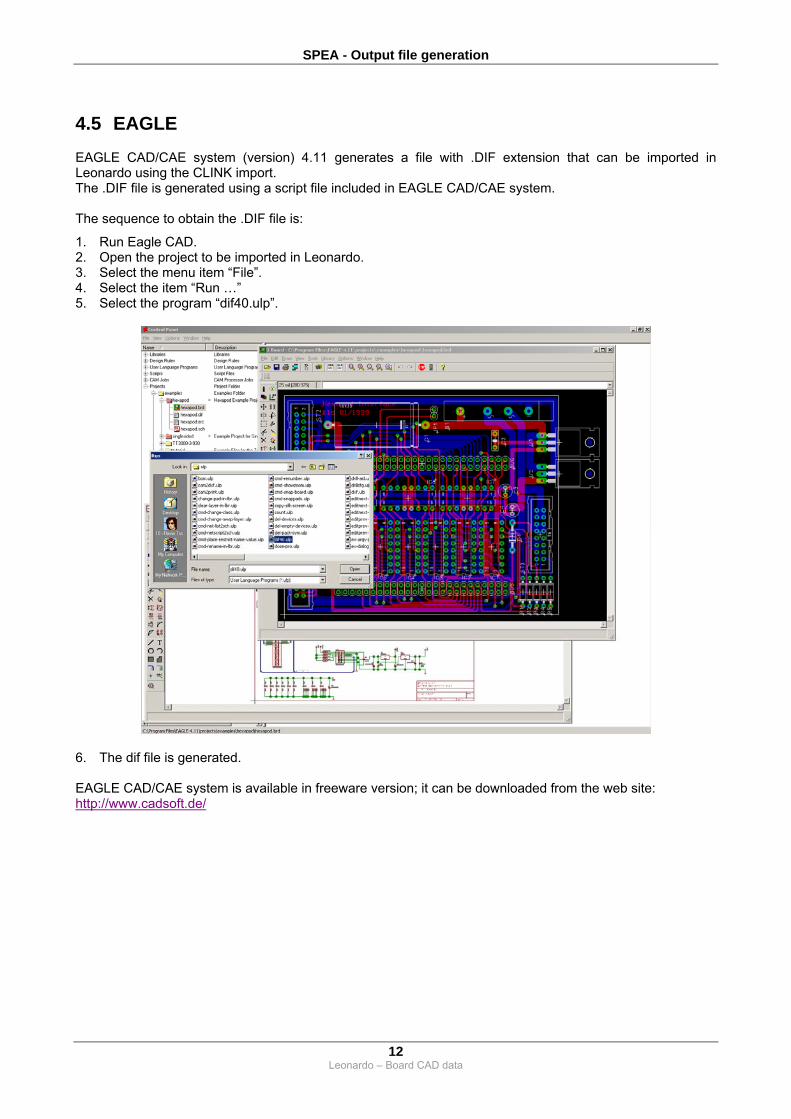
4.5 EAGLE
EAGLE CAD/CAE system (version) 4.11 generates a file with .DIF extension that can be imported in Leonardo using the CLINK import. The .DIF file is generated using a script file included in EAGLE CAD/CAE system. The sequence to obtain the .DIF file is:
1. Run Eagle CAD. 2. Open the project to be imported in Leonardo. 3. Select the menu item “File”. 4. Select the item “Run …” 5. Select the program “dif40.ulp”.
6. The dif file is generated. EAGLE CAD/CAE system is available in freeware version; it can be downloaded from the web site: http://www.cadsoft.de/

SPEA - Output file generation
13 Leonardo – Board CAD data
4.6 EASYPC
4.6.1 EasyPC ODB++ export
To export ODB++, data got to the menu Output – ODB++ in the window that opens, check the ‘Compressed’ box and ‘Select All’ layers:
Choose where you want to save the file using the browse entry box and this will create a compressed ‘tgz’ file which can be processed using the ODB++ input processor.
4.6.2 EasyPC Gencad export
To produce GENCAD from the menu Output – Export Gencad, select ‘Include Component values’ and ‘Include Copper’. It will default to using units ‘mm’ and ‘Use Design Coordinate Origin for all coordinates’, which are okay for Leonardo. Use the browse entry box to name the file and choose the folder location where you wish to save to. This will produce a Gencad file with a file extension of ‘cad’ which can be processed using the Gencad input processor.

SPEA - Output file generation
14 Leonardo – Board CAD data
4.7 MENTOR Expedition
It is very easy to extract a variety of data from Mentor Expedition: Use the menu item ‘File – Export – General Interfaces – Mitron Gencad’

SPEA - Output file generation
15 Leonardo – Board CAD data
4.8 ORCAD
To convert a printed circuit board, the database must be extracted as an ASCII file. To extract an ASCII file from ORCAD Layout for Windows: Go into File Menu | Export. Highlight the file format which is to be exported from the list. The OrCAD Layout for Windows format is MAX and to be exported into Test Expert the user should choose MAX Interchange.
In the editor MAX Board input, highlight the name of the .max file to be imported. In the example BUDDY_F1.max Click on Open.
The transition to the MAX Interchange Notation Output Editor is automatic. The name of the highlighted file is in the file name edit box and by default it is given the suffix .min. Click Save.
In the Options Editor, check the box "All of the above" to process everything in the file. Click the OK button.

SPEA - Output file generation
16 Leonardo – Board CAD data
In the Options Editor, check the box "All of the above" to process everything in the file. Click the OK button.
When the processing is completed the MIN Back Annotation Editor displays data relevant to the PCB such as: Original file name and location. Destination name and location. Number of layers, padstacks, nets, etc. If any errors occurred. … Click OK to return to the ORCAD Layout for Windows screen.

SPEA - Output file generation
17 Leonardo – Board CAD data
4.9 PADS
Before running the input processor, the database must be extracted from the PADS PCB CAD system as an ASCII file and transferred to the system where Leonardo is installed. To output an ASCII database from a PADS PCB CAD system: Select the menu: IN/OUT. Select ASCII OUT. Select the option: ALL. Select GO. These instructions will generate an ASCII output file with the extension .ASC. A sample listing of the contents of this file is supplied at the end of the datasheet. Note PADS POWER SUITE If using the PADS POWER Suite release, do NOT output the file in BASIC. Instead, use Mils. A sample of the header file follows. IPADS-POWERPCB-V1.5-MILS: DESIGN DATABASE ASCII FILE 1.0
*PCB* GENERAL PARAMETERS OF THE PCB DESIGN UNITS 0 2=Inches 1=Metric 0=Mils USERGRID 5 Space between USER grid points MAXIMUMLAYER 4 Maximum routing layer …
Example: Generating an ASCII File Using PADS PowerPCB V.1.5 Install the software PADS PowerPCB on the system where Test Expert has been set up.
In the pull-down menu, access File Menu | Export to display the window File Export listing the different files. If the name of the job is not proposed by default in the file name edit box, type it in manually. Enter the name of the file, for example <My_job>. Click on the Save button (or in French: Enregistrer).

SPEA - Output file generation
18 Leonardo – Board CAD data
To output an ASCII file containing the necessary data: Select Sections to Output Click the button Select All to check all the sections. Select Units Select Current Units. Special Options Select Include Attributes. Output Format Select PADS PowerPCB v1.5

SPEA - Output file generation
19 Leonardo – Board CAD data
4.10 Protel 3
Protel is now a very OLD system and has been superceded by Altium Designer Extracting Data from the Protel Client 99 System
Using Protel Client 99 the user should open the job file (board) and save it as a PCB ASCII file: In the menu bar open File | Save As. Select the file format: PCB ASCII File [*.PCB].

SPEA - Output file generation
20 Leonardo – Board CAD data
4.11 LabCentre PROTES ARES PCB layout
ODB++ is the supported manufacturing output format. On the main menu select ‘Output – ODB++ Output’ and then on the next screen choose : ‘All’ Layers/Artworks layer selection ‘Output to a single zip file ? Then choose your file name and output path using the Job Name and Folder browser boxes :

SPEA - Output file generation
21 Leonardo – Board CAD data
4.12 PULSONIX
4.12.1 Pulsonix ODB++ export
To export ODB++, data got to the menu Output – ODB++ in the window that opens, check the ‘Compressed’ box to generate the files into a compressed ‘tgz’ structure.
Do not check the ‘Use CAM/Plot Layer Combinations as this will not generate ALL the layers but will only output a sub-set as defined in the options settings :
4.12.2 Pulsonix Gencad export
From the Output menu, select the GenCAD option (this is a purchasable add-on option for this system), the dialog below is similar to that displayed below:
From this dialog, you can choose the name of the output file to be generated. The default for this name is the same as the name of your PCB design, with the file extension for GenCAD files as defined in the Options dialog

SPEA - Output file generation
22 Leonardo – Board CAD data
4.13 VERIBEST or EXPEDITION
In order to use the output file of these CAD/CAE system the following settings have to be performed:
1. The output file “VBPCBP.MDC” have to be renamed as “VBPCBP.MDB”. 2. The output has to be set as “Version 1” for Vevibest and “Version 2” for Expedition.
SPEA - Example of CAD data files
23 Leonardo – Board CAD data
5. Example of CAD data files
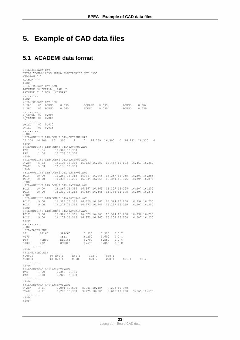
5.1 ACADEMI data format
:FIL=JOBDATA.DAT TITLE "COMM.12659 PRIMA ELECTRONICS CST 555" VERSION " " AUTHOR " " :EOD :FIL=PCBDATA.DAT[NAM] LAYNAME 00 "DRILL _ PAD " LAYNAME 01 " TOP _COPPER" .......... :EOD :FIL=PCBDATA.DAT[SIZ] S_PAD 00 ROUND 0.039 SQUARE 0.035 ROUND 0.004 S_PAD 01 ROUND 0.060 ROUND 0.039 ROUND 0.039 .......... S_TRACK 00 0.004 S_TRACK 01 0.006 .......... DRILL 00 0.020 DRILL 01 0.028 .......... :EOD :FIL=OUTLINE.LIB>CONN2.OTL>OUTLINE.DAT 16.300 16.300 60 300 1 2 16.369 16.300 0 16.232 16.300 0 :EOD :FIL=OUTLINE.LIB>CONN2.OTL>LAYER00.AWL PAD 1 56 16.369 16.300 PAD 1 56 16.232 16.300 :EOD :FIL=OUTLINE.LIB>CONN2.OTL>LAYER50.AWL TRACK 5 63 16.133 16.359 16.133 16.103 16.467 16.103 16.467 16.359 TRACK 5 63 16.133 16.359 :EOD :FIL=OUTLINE.LIB>CONN2.OTL>LAYER01.AWL POLY 10 00 16.267 16.315 16.267 16.265 16.257 16.255 16.207 16.255 POLY 10 00 16.334 16.265 16.334 16.365 16.344 16.375 16.394 16.375 :EOD :FIL=OUTLINE.LIB>CONN2.OTL>LAYER02.AWL POLY 10 00 16.267 16.315 16.267 16.265 16.257 16.255 16.207 16.255 POLY 10 00 16.334 16.265 16.334 16.365 16.344 16.375 16.394 16.375 :EOD :FIL=OUTLINE.LIB>CONN2.OTL>LAYER48.AWL POLY 9 00 16.329 16.365 16.329 16.265 16.344 16.250 16.394 16.250 POLY 9 00 16.272 16.365 16.272 16.265 16.257 16.250 16.207 16.250 :EOD :FIL=OUTLINE.LIB>CONN2.OTL>LAYER49.AWL POLY 9 00 16.329 16.365 16.329 16.265 16.344 16.250 16.394 16.250 POLY 9 00 16.272 16.365 16.272 16.265 16.257 16.250 16.207 16.250 :EOD .......... :EOD :FIL=PARTS.PRT SG1 SG160 SPEC60 5.925 5.525 0.0 T W175 TEST 6.250 5.600 0.0 T PZ9 +VBUS SP0165 6.700 5.550 0.0 T R103 2K2 SM0805 8.575 7.010 0.0 B .......... :EOD :FIL=WIRING.WIR N00001 04 R40.1 R41.1 IS2.2 W58.1 N00003 04 D27.1 U3.8 R20.2 W28.1 R21.1 C3.2 .......... :EOD :FIL=ARTWORK.ART>LAYER00.AWL PAD 1 00 6.350 7.125 PAD 1 00 7.925 6.350 .......... :EOD :FIL=ARTWORK.ART>LAYER01.AWL TRACK 3 11 8.091 10.570 8.091 10.484 8.225 10.350 TRACK 4 11 9.775 10.350 9.775 10.380 9.665 10.490 9.665 10.570 .......... :EOD :EOF

SPEA - Example of CAD data files
24 Leonardo – Board CAD data
5.2 ACCEL data format
ACCEL_ASCII "D:\RESAVE\DEMO\Accsampl.pcb" (asciiHeader (asciiVersion 2 2) (timeStamp 1997 7 11 9 7 24) (program "ACCEL P-CAD PCB" "13.00.35") (copyright "Copyright © 1997 ACCEL Technologies, Inc.") (fileAuthor "Ray Schnorr, Richard Crews") (headerString "License: 2009-3047 123456 Employee ACCEL 123456 Employee ACCEL") (fileUnits Mil) ) (library "Library_1" (padStyleDef "P:EX60Y60D38A" (holeDiam 38.0) (StartRange 1) (EndRange 2) (padShape (layerNumRef 1) (padShapeType Ellipse) (shapeWidth 60.0) (shapeHeight 60.0) ) (padShape (layerType Plane) (padShapeType Thrm4_45) (outsideDiam 76.0) (insideDiam 57.0) (spokeWidth 0.32173 mm) ) (padShape (layerType NonSignal) (padShapeType Ellipse) (shapeWidth 0.0) (shapeHeight 0.0) ) ) (viaStyleDef "V:Ex62y62d38a_bury" (holeDiam 38.0) (StartRange 13) (EndRange 18) (viaShape (layerNumRef 1) (viaShapeType Ellipse) (shapeWidth 0.0) (shapeHeight 0.0) ) (viaShape (layerNumRef 19) (viaShapeType Ellipse) (shapeWidth 0.0) (shapeHeight 0.0) ) ) (patternDef "JMP3_1" (originalName "JMP3") (multiLayer (pad (padNum 1) (padStyleRef "P:SX60Y60D38A")(pt 0.0 0.0) ) ) (layerContents (layerNumRef 6) (line (pt -50.0 -20.0) (pt -50.0 20.0) (width 10.0) ) (line (pt 250.0 -20.0) (pt 250.0 20.0) (width 10.0) ) (attr "Type" "" (pt -75.0 -169.0) (textStyleRef "T:H91W10") ) (attr "Value" "" (textStyleRef "BASIC60") ) (attr "RefDes" "" (pt -0.71124 mm 4.69904 mm) (rotation 270.0) (isVisible True) (textStyleRef "T:H91W10") ) ) ) (compDef "POT3T_1" (originalName "POT3T") (compHeader (sourceLibrary "") (numPins 3) (numParts 0) (alts (ieeeAlt False) (deMorganAlt False)) (refDesPrefix "") ) (compPin "1" (partNum 1) (symPinNum 1) (gateEq 0) (pinEq 0) ) (compPin "2" (partNum 1) (symPinNum 1) (gateEq 0) (pinEq 0) ) (compPin "3" (partNum 1) (symPinNum 1) (gateEq 0) (pinEq 0) ) (attachedPattern (patternNum 1) (patternName "POT3T") (numPads 3) (padPinMap (padNum 1) (compPinRef "1") (padNum 2) (compPinRef "2") (padNum 3) (compPinRef "3") ) ) ) ) ) (netlist "Netlist_1" (compInst "C2" (compRef "CAP100_1") (originalName "CAP100") (compValue "{Value}") ) )

SPEA - Example of CAD data files
25 Leonardo – Board CAD data
5.3 ARIADNE data format
*ARIADNE* DATEI INFORMATIONEN *VERSION* 7.7 pcb *UNIT* mil *PCB* Parameter-Einstellungen f�r PCB-Layout LANGUAGE GERMAN JOBNAME fom012.lay TITLE MAXIMUMLAYER 6 USERGRID 5 LASTGRID 1 DOTGRID 200 SCALE 5.993 ORIGIN 5000 5000 ..... *NETINFO* Parameter-Einstellungen f�r PCB-Layout NET * DISP DISPTRK DISPCON ROUTE RIPUP MIND NET GND DISP DISPTRK DISPCON ROUTE RIPUP MIND -WHITE -WHITE LGREEN NET GNDM DISP DISPTRK DISPCON ROUTE RIPUP MIND -WHITE -WHITE 22 NET SHIELD1 DISP DISPTRK DISPCON ROUTE RIPUP MIND -WHITE -WHITE 23 NET TERM1_PWR DISP DISPTRK DISPCON ROUTE RIPUP MIND -WHITE -WHITE LVIOLET NET TERM2_PWR DISP DISPTRK DISPCON ROUTE RIPUP MIND -WHITE -WHITE ORANGE *NETWIDTH* Parameter-Einstellungen f�r PCB-Layout NET * *FREEPADS* Frei definierte Pad-Entw�rfe *REMARK* Name Typ Bezugspunkt(X-Koord.,Y-Koord.) Lage Breite *REMARK* Art [<Option>] "LINE" or "FULL" *REMARK* X-Pos. Y-Pos. ["ARC" Radius] *REMARK* Bezugspunkt(X-Koord.,Y-Koord) Drehung Spiegelung H”he Breite Lage @PADPAD08051 PADDRW 0 0 <ALL> 8 CLOSED FULL -21.65354 -15.74803 5.90551 -15.74803 5.92519 0 ARC 15.74803 5.90551 15.74803 -21.65354 15.74803 -21.65354 -15.74803 END END ..... *PARTDECAL* TEILE *REMARK* Name Anz.-Terminals Anz.-Padbeschr. Breite Typ Best�ckungspunkt(X/Y) *REMARK* Art [<Option>] "LINE" or "FULL" *REMARK* X-Pos. Y-Pos. ["ARC" Radius] *REMARK* Bezugspunkt(X-Koord.,Y-Koord) Drehung Spiegelung H”he Breite Lage *REMARK* T X-Pos. Y-Pos. 0 Pinname(X-Pos. Y-Pos. Orientation [Mirror]) *REMARK* PAD PIN FINGER *REMARK* EBENE GROESSE FORM F-NP F-LAENGE F-VERSATZ BOHRUNG *REMARK* EBENE GROESSE FORM BOHRUNG @1210-R 2 1 10 <SMD> 0 0 NN -100 75 0 N 78 10 NT -100 -150 0 N 78 10 N1 100 0 0 N 78 10 N2 100 -75 0 N 78 10 N3 100 -150 0 N 78 10 TS 78 10 HEIGHT 71 T -55 0 0 -55 0 0 T 55 0 0 55 0 0 PAD <ALL> TOP 39 RF 90 110 0 0 0 SMT SAMETOP SMB NO PMB NO CLOSED SS LINE -80 -60 80 -60 80 60 -80 60 -80 -60 END OPEN AD LINE -15 40 -15 -40 END OPEN AD LINE

SPEA - Example of CAD data files
26 Leonardo – Board CAD data
15 40 15 -40 END OPEN AD LINE -30 0 -20 0 END OPEN AD LINE 15 0 25 0 END CIRCLE GMT FULL 10 0 -12 0 12 END ..... *PARTTYPE* TEILE *REMARK* Name Technologie Familie Zusatzzeilen Anzahl-Bauformen Anzahl-Gatter *REMARK* Gatter-Typ Tausch-Gruppe Anzahl-Pins *REMARK* Symbol-Pinnr.,Decal-Pinnr.,Pin-Name,Tausch-Gruppe,Pin-Typ,Signal,Breite @3K3 ANA 0! 2 18 1 # Class: R # Date : 07. OCT 98 :R040B010:R050B010:1206-R:1206-W:0805-R:0805-W:R030B010 :MINIMELF-R:MINIMELF-W:R020B017:MCR03-R:MCR03-W:R020B010 :R050B020:MELF-R:MELF-W:0603-R:0603-W G 0 2 :R-X:R-Y 1,1,1,1,U, 2,2,2,1,U, ..... *PART* TEILE *REMARK* 3K3 1210-R X Y NP FIX SPIEGELN NM-X NM-Y NM-NP @R25 75R:0805-R 1075 2500 0 N U NN 150 -50 90 N 51 6 N3 105 -220 0 N 40 4 TS 19 4 ... *ROUTE* LEITERBAHN *REMARK* *SIGNAL* SIGNALNAME MIT FLAGS *REMARK* BAUTEILNAME.PIN BAUTEILNAME.PIN *REMARK* X-Pos. Y-Pos. [Via-Nr/Type]Ebene SEGMENTBREITE *SIGNAL* $1 8 R1.2 C1.1 R 8650 4131.49606 L1 8650 4193.50393 END P1.U1 C1.1 R 8445.43307 4297.59842 L1 8445.43307 4285 8535 4195.43307 8650 4195.43307 8650 4193.50393 END ..... *NET* *SIGNAL* FPY_DRATE0 12 P6.E2 *SIGNAL* FPY_MSEN1 12 P6.D1 ..... *END* der ASCII-OUTPUT Datei

SPEA - Example of CAD data files
27 Leonardo – Board CAD data
5.4 CADDY data format
The following is a partial example of the CADDY text output files.
5.4.1 File: *.NEL +----------------------------------------------+ ▌Netzliste ▌ +----------------------------------------------▌ ▌NAME ▌NETZ ▌PIN-NR▌X ▌Y ▌ +--------+------------+------+--------+--------▌ ▌BCU101 ▌172 ▌ 1▌ 18.21▌ 24.91▌ ▌BCU101 ▌171 ▌ 2▌ 20.71▌ 24.91▌ ▌BCU101 ▌177 ▌ 3▌ 35.56▌ 4.76▌ ▌BCU101 ▌178 ▌ 4▌ 37.56▌ 4.76▌ ▌BCU101 ▌179 ▌ 5▌ 39.56▌ 4.76▌ ▌BCU101 ▌180 ▌ 6▌ 41.56▌ 4.76▌ ▌BCU101 ▌181 ▌ 7▌ 43.56▌ 4.76▌ ▌BCU101 ▌182 ▌ 8▌ 45.56▌ 4.76▌ ▌BCU101 ▌188 ▌ 9▌ 35.56▌ 7.31▌ ▌BCU101 ▌187 ▌ 10▌ 37.56▌ 7.31▌ ▌BCU101 ▌186 ▌ 11▌ 39.56▌ 7.31▌ ▌BCU101 ▌183 ▌ 12▌ 41.56▌ 7.31▌ ▌BCU101 ▌185 ▌ 13▌ 43.56▌ 7.31▌ ▌BCU101 ▌184 ▌ 14▌ 45.56▌ 7.31▌ ▌BCU101 ▌GND_BCU ▌ 15▌ 35.56▌ 23.21▌ ▌BCU101 ▌168 ▌ 16▌ 37.56▌ 23.21▌ ▌BCU101 ▌160d ▌ 17▌ 39.56▌ 23.21▌ ▌BCU101 ▌160e ▌ 18▌ 41.56▌ 23.21▌ …………………… ▌T202 ▌224 ▌ 3▌ 21.95▌ 113.98▌ ▌TP201 ▌+5V_B ▌ 1▌ 9.46▌ 116.58▌ ▌TP201 ▌GND_B ▌ 2▌ 14.54▌ 116.58▌ ▌TP201 ▌234 ▌ 3▌ 12.00▌ 106.42▌ ▌TP202 ▌+5V_B ▌ 1▌ 63.08▌ 114.04▌ ▌TP202 ▌GND_B ▌ 2▌ 63.08▌ 108.96▌ ▌TP202 ▌237 ▌ 3▌ 52.92▌ 111.50▌ ▌TR301 ▌304 ▌ 1▌ 30.80▌ 228.40▌ ▌TR301 ▌308 ▌ 2▌ 30.80▌ 216.97▌ ▌TR301 ▌GND_L ▌ 3▌ 48.58▌ 216.34▌ ▌TR301 ▌305 ▌ 4▌ 48.58▌ 229.04▌ +----------------------------------------------+
5.4.2 File: *.STL +----------------------------------------------------------------------------------------------------------------+ ¦Stückliste ¦ +----------------------------------------------------------------------------------------------------------------¦ ¦NAME ¦WERT ¦TYP ¦GEHÄUSE ¦X-GEHÄUSE ¦Y-GEHÄUSE ¦LAGE¦PIN-NR¦PIN-BEZ ¦X-PIN ¦Y-PIN ¦ +--------+---------+-------+--------------------+----------+----------+----+------+------------+--------+--------¦ ¦C106 ¦100nF ¦C ¦SMD-1206 ¦ 21.59¦ 63.50¦ 1¦ 1¦ ¦ 21.59¦ 62.05¦ ¦C106 ¦100nF ¦C ¦SMD-1206 ¦ 21.59¦ 63.50¦ 1¦ 2¦ ¦ 21.59¦ 64.95¦ ¦C107 ¦100nF ¦C ¦SMD-1206 ¦ 41.59¦ 63.82¦ 1¦ 1¦ ¦ 43.04¦ 63.82¦ ¦C107 ¦100nF ¦C ¦SMD-1206 ¦ 41.59¦ 63.82¦ 1¦ 2¦ ¦ 40.14¦ 63.82¦ ¦C108 ¦470nF ¦C ¦SMD-1206 ¦ 41.59¦ 61.28¦ 1¦ 1¦ ¦ 43.04¦ 61.28¦ ¦C108 ¦470nF ¦C ¦SMD-1206 ¦ 41.59¦ 61.28¦ 1¦ 2¦ ¦ 40.14¦ 61.28¦ ¦C109 ¦470nF ¦C ¦SMD-1206 ¦ 47.63¦ 60.80¦ 1¦ 1¦ ¦ 47.63¦ 59.35¦ ¦C109 ¦470nF ¦C ¦SMD-1206 ¦ 47.63¦ 60.80¦ 1¦ 2¦ ¦ 47.63¦ 62.25¦ ¦C110 ¦10nF ¦C ¦SMD-1206 ¦ 64.45¦ 60.96¦ 1¦ 1¦ ¦ 64.45¦ 62.41¦ ¦C110 ¦10nF ¦C ¦SMD-1206 ¦ 64.45¦ 60.96¦ 1¦ 2¦ ¦ 64.45¦ 59.51¦ ¦C111 ¦100nF ¦C ¦SMD-1206 ¦ 22.54¦ 57.47¦ 1¦ 1¦ ¦ 22.54¦ 56.02¦ ¦C111 ¦100nF ¦C ¦SMD-1206 ¦ 22.54¦ 57.47¦ 1¦ 2¦ ¦ 22.54¦ 58.92¦ ¦C112 ¦100nF ¦C ¦SMD-1206 ¦ 39.05¦ 52.71¦ 1¦ 1¦ ¦ 37.60¦ 52.71¦ …………………… ¦R132 ¦1,8k ¦R ¦SMD-1206 ¦ 16.83¦ 36.83¦ 1¦ 2¦ ¦ 16.83¦ 38.28¦ ¦R133 ¦47R ¦R ¦SMD-1206 ¦ 19.68¦ 36.83¦ 1¦ 1¦ ¦ 19.68¦ 35.38¦ ¦R133 ¦47R ¦R ¦SMD-1206 ¦ 19.68¦ 36.83¦ 1¦ 2¦ ¦ 19.68¦ 38.28¦ ¦R141 ¦10k ¦R ¦SMD-1206 ¦ 10.48¦ 19.37¦ 1¦ 1¦ ¦ 9.03¦ 19.37¦ ¦R141 ¦10k ¦R ¦SMD-1206 ¦ 10.48¦ 19.37¦ 1¦ 2¦ ¦ 11.93¦ 19.37¦ ¦R142 ¦1k ¦R ¦SMD-1206 ¦ 4.13¦ 16.51¦ 1¦ 1¦ ¦ 2.68¦ 16.51¦ ¦R142 ¦1k ¦R ¦SMD-1206 ¦ 4.13¦ 16.51¦ 1¦ 2¦ ¦ 5.58¦ 16.51¦ ¦R143 ¦100k ¦R ¦SMD-1206 ¦ 10.48¦ 16.51¦ 1¦ 1¦ ¦ 9.03¦ 16.51¦ ¦R143 ¦100k ¦R ¦SMD-1206 ¦ 10.48¦ 16.51¦ 1¦ 2¦ ¦ 11.93¦ 16.51¦ ¦T104 ¦BC857C ¦PNP ¦SOT23 ¦ 15.56¦ 31.75¦ 1¦ 1¦ ¦ 14.61¦ 30.75¦ ¦T104 ¦BC857C ¦PNP ¦SOT23 ¦ 15.56¦ 31.75¦ 1¦ 2¦ ¦ 16.51¦ 30.75¦ ¦T104 ¦BC857C ¦PNP ¦SOT23 ¦ 15.56¦ 31.75¦ 1¦ 3¦ ¦ 15.56¦ 32.75¦

SPEA - Example of CAD data files
28 Leonardo – Board CAD data
+----------------------------------------------------------------------------------------------------------------+

SPEA - Example of CAD data files
29 Leonardo – Board CAD data
5.5 CADENCE data format
The following is a partial example of a CADENCE ASCII text output file. A!REFDES!COMP_CLASS!COMP_PART_NUMBER!COMP_HEIGHT!COMP_DEVICE_LABEL!COMP_INSERTION_CODE!SYM_TYPE!SYM_NAME!SYM_MIRROR!SYM_ROTATE!SYM_X!SYM_Y!COMP_VALUE!COMP_TOL!COMP_VOLTAGE!COMP_RATED_CURRENT!COMP_RATED_POWER!COMP_RATED_VOLTAGE! J!/usr/local_users/tronzano/ext/hybrid.brd!Thu Jul 20 14:05:58 2000!-100.000!-121.600!250.000!178.400!0.001!millimeters!TOP!21.4667 mil!21!UP TO DATE! S!U6!IC!520366230358!!U_XB_MEF_ALT-520366230257!!PACKAGE!UM29F100T_AG!NO!0.000!6.150!27.850!!!!!!5.5! S!U3!IC!520366501246!!U_CB_MPA_..ZCC439620HS20T!!PACKAGE!UALTAIR_AG!NO!0.000!24.400!25.400!!!!!!6.5! S!F1!DISCRETE!520368010056!!F_....ACT-4532-102A-2P-TL!!PACKAGE!VACT4532_AG!NO!0.000!19.150!4.250!!!!!!! S!U4!IC!520366350938!!U_XB_CUS_.....MAR9170DIE1!!PACKAGE!UL9170_AG!NO!180.000!44.800!17.000!!!!!!16! S!C1!DISCRETE!520361403156!!C_CC1C_..15PF..+- 5%_.50V!!PACKAGE!C0805_AG!NO!180.000!17.100!11.700!15PF!5%!CMAX!!!50V! S!C37!DISCRETE!520361403156!!C_CC1C_..15PF..+- 5%_.50V!!PACKAGE!C0805_AG!NO!180.000!17.100!13.600!15PF!5%!CMAX!!!50V! S!C9!DISCRETE!520361403181!!C_CC1C_..27PF..+-.5%_.50V!!PACKAGE!C0805_AG!NO!0.000!26.300!10.350!27PF!5%!CMAX!!!50V! ………………………… S!R54!DISCRETE!!!!!PACKAGE!HYBRES54!NO!270.000!34.650!16.550!!!CMAX!!!! S!R55!DISCRETE!!!!!PACKAGE!HYBRES55!NO!270.000!38.500!32.900!!!CMAX!!!! S!R6!DISCRETE!!!!!PACKAGE!HYBRES6!NO!0.000!25.000!7.750!!!CMAX!!!! S!R8!DISCRETE!!!!!PACKAGE!HYBRES8!NO!180.000!17.825!19.425!!!!!!! S!R90!DISCRETE!!!!!PACKAGE!HYBRES90!NO!270.000!32.750!15.150!!!!!!! ………………………… A!NET_NAME!REFDES!PIN_NUMBER!PIN_NAME!PIN_GROUND!PIN_POWER! J!/usr/local_users/tronzano/xtc/hybrid.brd!Thu Jul 20 14:06:01 2000!-100.000!-121.600!250.000!178.400!0.001!millimeters!TOP!21.4667 mil!21!UP TO DATE! S!ADB0!U6!33!A<0>!!! S!ADB10!U6!20!A<10>!!! S!ADB11!U6!19!A<11>!!! ………………………… S!UN2HYBRIDCONN109PA0!R77!2!B<0>!!! S!ROT+!R78!1!A<0>!!! S!UN2HYBRIDCONN107PA0!R78!2!B<0>!!! S!STS+!R79!1!A<0>!!! ………………………… S!UN2HYBRIDCONN106PA0!R79!2!B<0>!!! S!VCC!R8!1!A<0>!!! S!MODCK!R8!2!B<0>!!! S!VCC!R90!1!A<0>!!! S!UN2HYB1TCA80122W274PPIN0!R90!2!B<0>!!! A!CLASS!SUBCLASS! J!/usr/local_users/tronzano/ext/hybrid.brd!Thu Jul 20 14:06:02 2000!-100.000!-121.600!250.000!178.400!0.001!millimeters!TOP!21.4667 mil!21!UP TO DATE! S!BOARD GEOMETRY!ASSEMBLY_NOTES! S!BOARD GEOMETRY!DIMENSION! S!BOARD GEOMETRY!OUTLINE! ………………………… S!ROUTE KEEPOUT!SURFACE! S!TOLERANCE!ASSEMBLY_TOP! A!PAD_NAME!REC_NUMBER!LAYER!FIXFLAG!VIAFLAG!PADSHAPE1!PADWIDTH!PADHGHT!PADXOFF!PADYOFF!PADFLASH!PADSHAPENAME!TRELSHAPE1!TRELWIDTH!TRELHGHT!TRELXOFF!TRELYOFF!TRELFLASH!TRELSHAPENAME!APADSHAPE1!APADWIDTH!APADHGHT!APADXOFF!APADYOFF!APADFLASH!APADSHAPENAME! J!/usr/local_users/tronzano/ext/hybrid.brd!Thu Jul 20 14:06:07 2000!-100.000!-121.600!250.000!178.400!0.001!millimeters!TOP!21.4667 mil!21!UP TO DATE! S!AU_800_1000!00001!SURFACE!f!v!!0.000!0.000!0.000!0.000!!!!0.000!0.000!0.000!0.000!!!!0.000!0.000!0.000!0.000!!! S!AU_800_1000!00002!internal_pad_def!f!v!!0.000!0.000!0.000!0.000!!!!0.000!0.000!0.000!0.000!!!!0.000!0.000!0.000!0.000!!! S!AU_800_1000!00005!AU!f!v!RECTANGLE!0.800!1.000!0.000!0.225!!!!0.000!0.000!0.000!0.000!!!!0.000!0.000!0.000!0.000!!! S!AU_800_1000!00006!QM34!f!v!!0.000!0.000!0.000!0.000!!!!0.000!0.000!0.000!0.000!!!!0.000!0.000!0.000!0.000!!! ………………………… S!PIN400_1550MIC-1!00028!~BFM!o!!!0.000!0.000!0.000!0.000!!!!!!!!!!!!!!!!! S!PIN400_1550MIC-1!00029!~DRILL!o!!0.000!0.000!0.000!0.000!0.000!!P!!!!!!!!!!!!!!! A!GRAPHIC_DATA_NAME!GRAPHIC_DATA_NUMBER!RECORD_TAG!GRAPHIC_DATA_1!GRAPHIC_DATA_2!GRAPHIC_DATA_3!GRAPHIC_DATA_4!GRAPHIC_DATA_5!GRAPHIC_DATA_6!GRAPHIC_DATA_7!GRAPHIC_DATA_8!GRAPHIC_DATA_9!SUBCLASS!SYM_NAME!REFDES! J!/usr/local_users/tronzano/ext/hybrid.brd!Thu Jul 20 14:06:10 2000!-100.000!-121.600!250.000!178.400!0.001!millimeters!TOP!21.4667 mil!21!UP TO DATE! S!LINE!257!6911 1!41.100!9.038!41.100!10.104!0.000!!!!!ASSEMBLY_TOP!!! S!LINE!257!6911 2!41.100!10.104!42.048!10.104!0.000!!!!!ASSEMBLY_TOP!!! S!LINE!257!6911 5!41.602!9.044!41.097!9.044!0.000!!!!!ASSEMBLY_TOP!!! ………………………… A!SYM_NAME!PIN_NAME!PIN_NUMBER!PIN_X!PIN_Y!PAD_STACK_NAME!REFDES!TEST_POINT! J!/usr/local_users/tronzano/ext/hybrid.brd!Thu Jul 20 14:06:13 2000!-100.000!-121.600!250.000!178.400!0.001!millimeters!TOP!21.4667 mil!21!UP TO DATE! S!HYBRES90!A<0>!1!33.600!14.950!PIN400_1700MIC!R90!! S!HYBRES79!B<0>!2!48.200!21.800!PIN400_1500MIC!R79!! ………………………… A!VIA_X!VIA_Y!PAD_STACK_NAME!NET_NAME!TEST_POINT! J!/usr/local_users/tronzano/ext/hybrid.brd!Thu Jul 20 14:06:15 2000!-100.000!-121.600!250.000!178.400!0.001!millimeters!TOP!21.4667 mil!21!UP TO DATE! S!14.000!8.650!T1!UN3FILTER08395PF2A0!!

SPEA - Example of CAD data files
30 Leonardo – Board CAD data
S!14.950!9.400!T1!UN3FILTER08395PF1A0!! S!25.900!16.950!T4!CLKOUT!! S!22.750!16.775!T3!XTAL!! ………………………… A!CLASS!SUBCLASS!GRAPHIC_DATA_NAME!GRAPHIC_DATA_NUMBER!RECORD_TAG!GRAPHIC_DATA_1!GRAPHIC_DATA_2!GRAPHIC_DATA_3!GRAPHIC_DATA_4!GRAPHIC_DATA_5!GRAPHIC_DATA_6!GRAPHIC_DATA_7!GRAPHIC_DATA_8!GRAPHIC_DATA_9!NET_NAME! J!/usr/local_users/tronzano/ext/hybrid.brd!Thu Jul 20 14:06:17 2000!-100.000!-121.600!250.000!178.400!0.001!millimeters!TOP!21.4667 mil!21!UP TO DATE! S!ETCH!TOP!LINE!257!1 1 0!21.663!7.639!22.563!6.565!0.000!!!!!! S!ETCH!TOP!LINE!257!1 2 0!22.563!6.565!22.027!6.115!0.000!!!!!! S!ETCH!TOP!LINE!257!1 3 0!22.027!6.115!21.127!7.189!0.000!!!!!! …………………………
5.5.1 REMARK
The CADENCE ALLEGRO CAD-CAE runs under Unix operating system and generates its neutral ASCII output file in Unix format. The Unix ASCII text files use as end of line identifier, the ASCII character "0ahex". The Windows (MS-DOS) operating system uses for ASCII text files, as end of line identifier, the ASCII characters "0dhex" and "0ahex". This means that output ASCII text files may require an ASCII format conversion (from Unix to Windows format). This operation can be performed using "WordPad". Open the CADENCE ALLEGRO ASCII file with this editor and save it; this operation will automatically perform the conversion from ASCII Unix format to ASCII Windows format.
5.5.2 Example of CADENCE ALLEGRO extraction script
The format of this ASCII text output file is the result of a customizable output in CADENCE ALLEGRO CAD-CAE. In order to create it a specific Unix script has to be used, in the following lines a partial example of this script is listed. #! /bin/sh #------------------------ # PIN_ROTATION (PADSTACK) #-------------------------------- # If user attribut "PIN_ROTATION" is present in your DATABASE you can add # in section SYMBOLS this field. # the Format in 2.3 in degrees like !90.000! (trigonometric-anticlockwise) # the angle is referenced to the component(a zero degrees) # This Field allow to get a good result for padstack rotation in package. # COMPONENTS ATTRIBUTES #--------------------- # For components attributes, you can add any field in the first section as: # COMP_VALUE,COMP_TOL,COMP_RATED_VOLTAGE,COMP_RATED_POWER... # # This routine uses the "EXTRACT" command on a VALID ALLEGRO CADENCE # System ……………………………………… # -------------------------------------- # PARTS SECTION echo "COMPONENT REFDES COMP_CLASS COMP_PART_NUMBER COMP_HEIGHT COMP_DEVICE_LABEL COMP_INSERTION_CODE SYM_TYPE SYM_NAME SYM_MIRROR SYM_ROTATE SYM_X SYM_Y COMP_VALUE COMP_TOL COMP_VOLTAGE COMP_RATED_CURRENT COMP_RATED_POWER COMP_RATED_VOLTAGE" > parts$$.txt ……………………………………… # -------------------------------------- # NETS SECTION echo "COMPONENT_PIN NET_NAME REFDES

SPEA - Example of CAD data files
31 Leonardo – Board CAD data
PIN_NUMBER PIN_NAME PIN_GROUND PIN_POWER" > nets$$.txt ……………………………………… # -------------------------------------- # LAYERS SECTION echo "GEOMETRY CLASS!=\"VIA CLASS\" CLASS!=\"PIN\" CLASS!=\"PACKAGE GEOMETRY\" CLASS!=\"ETCH\" OR CLASS=\"ETCH\"" > layers$$.txt echo "LAYER LAYER_USE=\"EMBEDDED_PLANE\" LAYER_SUBCLASS" > ex$$.txt ……………………………………… # -------------------------------------- # PAD STACKS SECTION echo "PAD_DEF" > pads$$.txt extract -q $CARTE pads$$.txt fab$$.dat cat fab$$.dat >> $OUT # -------------------------------------- # SYMBOL SECTION echo "GEOMETRY CLASS=\"PACKAGE GEOMETRY\" GRAPHIC_DATA_NAME GRAPHIC_DATA_NUMBER RECORD_TAG GRAPHIC_DATA_1 GRAPHIC_DATA_2 GRAPHIC_DATA_3 GRAPHIC_DATA_4 GRAPHIC_DATA_5 GRAPHIC_DATA_6 GRAPHIC_DATA_7 GRAPHIC_DATA_8 GRAPHIC_DATA_9 SUBCLASS SYM_NAME REFDES" > symbols$$.txt extract -q $CARTE symbols$$.txt fab$$.dat cat fab$$.dat >> $OUT # --------------------------------------
# SYMBOLS SECTION COMPONENT VIA echo "COMPOSITE_PAD CLASS!=\"VIA CLASS\" SYM_NAME PIN_NAME PIN_NUMBER PIN_X PIN_Y PAD_STACK_NAME REFDES PIN_ROTATION TEST_POINT" > compvia$$.txt ……………………………………… # -------------------------------------- # PADS SECTION echo "COMPOSITE_PAD CLASS=\"VIA CLASS\" VIA_X VIA_Y PAD_STACK_NAME NET_NAME TEST_POINT" > vias$$.txt extract -q $CARTE vias$$.txt fab$$.dat cat fab$$.dat >> $OUT # -------------------------------------- # GEOMETRY SECTION echo "GEOMETRY CLASS!=\"VIA CLASS\" CLASS!=\"PIN\" CLASS!=\"PACKAGE GEOMETRY\" CLASS!=\"ETCH\" OR CLASS=\"ETCH\"" > geo$$.txt ……………………………………… CLASS SUBCLASS GRAPHIC_DATA_NAME GRAPHIC_DATA_NUMBER RECORD_TAG GRAPHIC_DATA_1 GRAPHIC_DATA_2 GRAPHIC_DATA_3 GRAPHIC_DATA_4 GRAPHIC_DATA_5

SPEA - Example of CAD data files
32 Leonardo – Board CAD data
GRAPHIC_DATA_6 GRAPHIC_DATA_7 GRAPHIC_DATA_8 GRAPHIC_DATA_9 NET_NAME" >> geo$$.txt ……………………………………… # -------------------------------------- # PADS USER SHAPE SECTION echo "FULL_GEOMETRY CLASS=PIN SUBCLASS PAD_SHAPE_NAME GRAPHIC_DATA_NAME GRAPHIC_DATA_NUMBER RECORD_TAG GRAPHIC_DATA_1 GRAPHIC_DATA_2 GRAPHIC_DATA_3 GRAPHIC_DATA_4 GRAPHIC_DATA_5 GRAPHIC_DATA_6 GRAPHIC_DATA_7 GRAPHIC_DATA_8 GRAPHIC_DATA_9 GRAPHIC_DATA_10=SHAPE PAD_STACK_NAME REFDES ………………………………………

SPEA - Example of CAD data files
33 Leonardo – Board CAD data
5.6 CADSTAR, ZUKEN and VISULA CAD data format (CADIF)
The following is a partial example of a Cadif ASCII text output file, this format it is supported by Cadstar, Zuken and Visula CAD/CAE systems. (cadif (format CADIF 4 0) (design (dataSet ARCHIVE ROUTE_RULES PLACE_RULES) (paper (name "A3") (box (pt -21000000 -14850000) (pt 21000000 14850000)) (designOrigin (pt 0 0)) (paperScale (e 1 0))) (signalList (signal S1 (name "15V_DTMA") (spurMiter 127000)) (signal S2 (name "15V_DTMB") (spurMiter 127000)) (signal S3 (name "20W1") (spurMiter 127000)) (signal S4 (name "20W2") (spurMiter 127000)) (signal S5 (name "20W3") (spurMiter 127000)) ……………… (padCode PC37 (name "PLRR2512") (padCodeDesc (padAssign PS37 (layerRef L1)) (padStack TOP (pad PS37 L1)) (padStack BOTTOM (pad PS37 L20)))) (padCode PC38 (name "PLSMR1") (padCodeDesc (padAssign PS30 (layerRef L1)) (padStack TOP (pad PS30 L1)) (padStack BOTTOM (pad PS30 L20)))) (padCode PC39 (name "PLSMR3") (padCodeDesc ……………… (via V2 (position (pt -6762750 -4064000)) (padCodeRef PC54) (layerRange L1 L20) (fixed)) (via V3 (position (pt 4889500 -5715000)) (padCodeRef PC52) (layerRange L1 L8) (fixed)) (via V4 (position (pt 7810500 -4603750)) (padCodeRef PC52) (layerRange L1 L8) (fixed)) (via V5 (position (pt 9398000 -6191250)) (padCodeRef PC52) (layerRange L1 L8) ………………

SPEA - Example of CAD data files
34 Leonardo – Board CAD data
5.7 C-LINK data format
The following is a partial example of a C-LINK ASCII text output file. { JOB POWERPCB { PCB tele_65_82 { ENVIRONMENT { SOURCE "PADS-POWERPCB-V3.0" } { VERSION 4.3 } { DATE 21/8/2000 } { TIME 20: 0:12 } { UNITS 1/10000 mm } { LAYER 8 } { TOP_LAYER 1 } { BOTTOM_LAYER 8 } { NO_NET 552 } { NO_COMP 3176 } } { BOARD { F { L (0,0) (0,210000) (355000,210000) (355000,1380000) (1995000,1380000) (1995000,0) (940000,0) (940000,1000) } { L (910000,1000) (910390,3517) (911199,5932) (912405,8176) (913972,10184) (915855,11899) (918001,13271) (920347,14262) (922827,14842) (925370,14995) (927902,14717) (930350,14016) (932645,12911) (934721,11435) (936518,9630) (937984,7547) (939077,5246) (940000,1000) } { L (910000,1000) (910000,0) (0,0) } } } { PAD_DEF { PAD 0 { SIZE 10000 } { DRILL 0 } } ………………………… { PAD 1 { SIZE 19050 } { DRILL 0 } } ………………………… { NET_DEF { NET BATTERY_PLUS { W (1739000,1220500) 8 6500 (1715000,1220500) 8 6500 (1685000,1190500) 8 6500 (1299100,1190500) 8 6500 (1245000,1244600) 8 6500 } { W (1245000,1244600) 8 2000 (1219200,1244600) 8 2000 } { PIN -1 { TYP ICT } { TEST_PIN_SIDE 2 } { PLOC (1219200,1244600) } { SLOC { NAME TP89 } { PIN 1 } } } ………………………… { NET MCA10 { W (1110000,910000) 1 1500 (1097000,910000) 5 1500 (1164000,910000) 5 1500 (1229000,845000) 5 1500 (1346000,845000) 5 1500 (1351000,840000) 1 1500 (1351000,871000) 1 1500 (1350675,871000) 1 1500 } { W (1110000,910000) 1 1500 (1097000,910000) 5 1500 (1164000,910000) 5 1500 (1229000,845000) 5 1500 (1346000,845000) 5 1500 (1351000,840000) 8 1500 (1351000,858800) 8 1500 (1346200,863600) 8 1500 } { V (1097000,910000) 45 1, 8 } { V (1351000,840000) 45 1, 8 } { PIN -1 { TYP ICT } { TEST_PIN_SIDE 2 } { PLOC (1346200,863600) } { SLOC { NAME TP164 } { PIN 1 } } } }

SPEA - Example of CAD data files
35 Leonardo – Board CAD data
………………………… { COMPONENTS { COMP { COMP_DEF { NAME BU1 } { PART_NR UNBESTDIV }
} { PIN_DEF } { PICTURE { ORIGIN (1701800,123825) } { PIC 4 } { ROTATION 0 } { M_SIDE 2 } } } ………………………… { COMP { COMP_DEF { NAME C10 } { PART_NR V2666-Z4622-K2 } } { PIN_DEF { PIN 1 { NET POWER } { ICT -1 } } { PIN 2 { NET GND } { ICT -1 } } } { PICTURE { ORIGIN (1931988,493713) } { PIC 9 } { ROTATION 90 } { M_SIDE 1 } { KIND SMD } } } { COMP { COMP_DEF { NAME R172 } { PART_NR V1615-Z1310-F1 } } { PIN_DEF { PIN 1 { NET $$$22313 } { ICT -1 } } { PIN 2 { NET L_DISP } { ICT -1 } } } { PICTURE { ORIGIN (391000,605000) } { PIC 11 } { ROTATION 0 } { M_SIDE 1 } { KIND SMD } } } { COMP { COMP_DEF { NAME R173 } { PART_NR UNBESTDIV } } { PIN_DEF { PIN 1 { NET VDD_DISPLAY } } { PIN 2 { NET +3V3 } { ICT -1 } } } { PICTURE { ORIGIN (464000,515000) } { PIC 11 } { ROTATION 0 } { M_SIDE 1 } { KIND SMD } } } ………………………… } } }

SPEA - Example of CAD data files
36 Leonardo – Board CAD data
5.8 DDE data format
filename : /usr/ipl/iplsave/fab-mast operator : ipladm progversion : 6.1 x,y,lay,mul,div : 300000 300000 2 1 / 40 date : Tue Aug 20 09:32:02 1996 commentfile : null jobdepend. : null prepostpro. : '#(postpro)' .rem .psh padshapes : padshapenumber drillsize plated/non filled/non shapename .tsh tracksha : trackshapenumber filled/non shapename .tol tolerance string .cle deltasizes: number track- via- pad- smddelta .sec secret : secret shape .dfa def area : kind lay shape dir spacing groupname .coo coordinate: x y .cir circle : radius .poe pol end : end polygon name .pst padstack : padstacknumber drillsize plated/non filled/non \ stacktype padstackname .uls lay shape : userlaytypename shapenumber .pla plane info: deltaheat deltaiso heatgap clearance heatsymbol \ isosymbol calcheat calciso calcfromplotter .pse stack end : end padstack information .lpm lay assoc.: userlaytypename systemlaytypename polygon .cen arc center: x y rot .ena end area .fon textfont .typ type : xref yref xmax ymax typenumber typename .lay layattrib.: lay obstruction electric protection layname pastackname .sys sysparms : sysparmname sysparmvalue .cmd iplcommand: cmdname parmname1 parmvalue 1...nameX valueX .mir mirrormap : fromlay tolay .bma burymap : /fromlay;tolay;../fromlay;tolay .com component : compnum x y dir lay mir/not fix/visi stat tnum typename .cop comp opts : optionname optionvalue .blo blockname : compnum compnum ... compnum .wlg wlgroup : status protect/non groupname .wop wloptions : optionname optionvalue .pul paduselay : laylist .wlp wlistpin : compnum x y norm/sing/diff/pstack paddir pinnum compname \ [padstacknumber] layer shape ( 1-255 times ) .pop pin opts : optionname optionvalue .wle end wirelist .pad via : padshapenum x y layer paddirection .bur buried via: psha,psha,.. x y lay,lay,.. paddirection .tra track : trackshapenum xstart ystart xend yend layer .txt text : textx texty layer tdir tmir options tsize trackshapenum text .arc arc : arcx arcy layer radius alpha beta trackshapenum .end end .lay 0 oe 0 .lay 1 oe 1 .lay 201 d 201 .lay 255 oe 255 .mir 0 1 .mir 8 9 .mir 11 12 .mir 103 104 .mir 10 110 .mir 111 112 .mir 244 245 .mir 246 247 .mir 248 249 .mir 251 252 .mir 253 254 .psh 0 1969 p f v1,0-0,5 .cir 1969 .poe end plotterpolygon .cir 2362 .poe end electricpolygon .cir 1969 .poe end graphicpolygon .cir 1575

SPEA - Example of CAD data files
37 Leonardo – Board CAD data
.poe end solderpolygon
.cir 984
.poe end drillpolygon
.cir 1969
.poe end 8polygon
.coo 1575 0
.coo 0 1575
.coo -1575 0
.coo 0 -1575
.poe end 9polygon .psh 1 0 p f s160,060 .cle 1 0 0 0 0 .cle 2 0 0 0 0 .cle 3 0 0 800 800 .coo 3145 1180 .coo -3145 1180 .coo -3145 -1180 .coo 3145 -1180 .poe end plotterpolygon .coo 3535 1570 .coo -3535 1570 .coo -3535 -1570 .coo 3535 -1570 .poe end electricpolygon .coo 3145 1180 .coo -3145 1180 .coo -3145 -1180 .coo 3145 -1180 .poe end graphicpolygon .coo 3535 1570 .coo -3535 1570 .coo -3535 -1570 .coo 3535 -1570 .poe end solderpolygon .coo 2750 790 .coo -2750 790 .coo -2750 -790 .coo 2750 -790 .poe end 1polygon .cir 200 .poe end 2polygon .coo 3935 1975 .coo -3935 1975 .coo -3935 -1975 .coo 3935 -1975 .poe end 8polygon .coo 3145 1180 .coo -3145 1180 .coo -3145 -1180 .coo 3145 -1180 .poe end 9polygon .psh 2 3150 p f p1,4-0,8 .cle 1 0 0 0 0 .cle 2 0 0 800 800 .cle 3 0 0 0 0 .cir 2750 .poe end plotterpolygon .cir 3150 .poe end electricpolygon .cir 2750 .poe end graphicpolygon .cir 3150 .poe end solderpolygon .cir 1570 .poe end drillpolygon .cir 200 .poe end 2polygon .cir 3545 .poe end 8polygon .coo 2750 2750 .coo -2750 2750 .coo -2750 -2750 .coo 2750 -2750 .poe end 9polygon .tsh 0 f tr0,2 .cir 393 .poe end plotterpolygon .cir 787 .poe end electricpolygon .cir 393 .poe end graphicpolygon

SPEA - Example of CAD data files
38 Leonardo – Board CAD data
.cir 394
.poe end 8polygon
.coo 197 197
.coo -197 197
.coo -197 -197
.coo 197 -197
.poe end 9polygon .tsh 4 f silk .cir 390 .poe end plotterpolygon .cir 40 .poe end electricpolygon .cir 40 .poe end graphicpolygon .coo 40 40 .coo -40 40 .coo -40 -40 .coo 40 -40 .poe end 8polygon .coo 40 40 .coo -40 40 .coo -40 -40 .coo 40 -40 .poe end 9polygon .typ 4060 35000 30630 40000 2 /usr/ipl/ipltypes/smd/SO14-225 .tra 4 30630 37500 30630 40000 10 .tra 4 30630 0 30630 2500 10 .tra 4 26560 0 26560 40000 10 .tra 4 21560 2500 21560 37500 103 .tra 4 9060 2500 9060 37500 103 .tra 4 4060 0 4060 35000 10 .tra 4 0 37500 0 40000 10 .tra 4 0 0 0 2500 10 .tra 4 4060 35000 9060 40000 10 .tra 4 28130 40000 30630 40000 10 .tra 4 9060 40000 26560 40000 10 .tra 4 0 40000 2500 40000 10 .tra 4 9060 37500 21560 37500 103 .tra 4 21560 35000 26560 35000 103 .tra 4 4060 35000 9060 35000 103 .tra 4 21560 30000 26560 30000 103 .tra 4 4060 30000 9060 30000 103 .tra 4 21560 25000 26560 25000 103 .tra 4 4060 25000 9060 25000 103 .tra 4 21560 20000 26560 20000 103 .tra 4 4060 20000 9060 20000 103 .tra 4 21560 15000 26560 15000 103 .tra 4 4060 15000 9060 15000 103 .tra 4 21560 10000 26560 10000 103 .tra 4 4060 10000 9060 10000 103 .tra 4 21560 5000 26560 5000 103 .tra 4 4060 5000 9060 5000 103 .tra 4 9060 2500 21560 2500 103 .tra 4 28130 0 30630 0 10 .tra 4 4060 0 26560 0 10 .tra 4 0 0 2500 0 10 .arc 11560 35000 103 2000 0 360 4 .com 1 60000 155000 0 0 n n 0 2 /usr/ipl/ipltypes/smd/SO14-225 .txt 68610 152290 111 3 0 LB 6670 4 U01 .txt 67500 150000 14 3 0 LB 70 4 U-74LS74/OS .txt 67500 150000 15 3 0 LB 70 4 74LS74 .txt 68610 152290 103 3 0 LB 6670 4 U01 .com 2 132500 167500 0 0 n n 0 1 /usr/ipl/ipltypes/lead/DIP14 .txt 137500 175000 11 0 0 LB 6670 4 U02 .txt 140000 170000 15 3 0 LB 3000 4 DIP-SWITCH .txt 142500 170000 14 3 0 LB 3000 4 S-AA010 .txt 142500 162500 103 3 0 LB 8000 4 U02 .pad 0 65000 170000 255 0 .pad 0 102500 140000 255 0 .pad 0 102500 157500 255 0 .pad 0 117500 152500 255 0 .end

SPEA - Example of CAD data files
39 Leonardo – Board CAD data
5.9 DOCICA data format
IDEN21406328ABBA 01 -- 000 DTRF 01 SV01.00.05 PDESDTRF PSS HW STANDARDIZATION GENE 950201 CNNP 211CNB94091501SH46 LVDB V4.1 PROJ1240 PBT1 655 16 PROFATM S120655A-1 0 0 00 1526 3329 PBT2 2000 2500 101500 89500 HOLB 100000 88000 300N z1 L1AG000090001 HOLB 4000 4000 300N z3 L1AG000090001 HOLB 4000 88000 300N z2 L1AG000090001 ! FIDB 7000 86500 160KKF185P --------------FB2 1801AG000080002 FIDB 7000 5500 160KKF185P --------------FB1 1801AG000080002 FIDB 97000 86500 160KAF185P --------------FB7 1801AG000080002 FIDB 98000 5500 160KKF185P --------------FB4 1801AG000080002 FIDB 7000 86500 160KAF185P --------------FB6 1801AG000080002 FIDB 97000 86500 160KKF185P --------------FB3 1801AG000080002 FIDB 7000 5500 160KAF185P --------------FB5 1801AG000080002 FIDB 98000 5500 160KAF185P --------------FB8 1801AG000080002 ! NLMC21406327AAFA 1 1.PB-DTRF -------- NLMC21103500AAAA 3 1.MA-STIFFENER, ASSY. -------- NLMC21103502AAAA 4 1.MPP-LABEL -------- NLMC1AD001620019 5 4.RIVET*ROUND*TUBULAR -------- NLMC004212122505 6 2.RIVET-RND TUB 2,5X5 -------- NLMC21102984AAEA 8 1.MPP-LABEL (BARCODE) -------- NLMC1AB012650001 (1E) 109 1.IC-SOCKET*QFP*100W -------- NLMC1AB000050009 X4C 108 1.IC-SOCKET*DIL*32W -------- NLMC1AB000050009 X4D 108 1.IC-SOCKET*DIL*32W -------- NLMC1AD003530001 CL247X 115 1.CRYSTAL HOLDER CLIP -------- NLMC1AD003530001 CL346X 115 1.CRYSTAL HOLDER CLIP -------- NLMC1AD003530001 CL1302X 115 1.CRYSTAL HOLDER CLIP -------- NLMC21189672AAAA CL2471 198 1.MPP-CRYSTAL SPACER -------- NLMC21189672AAAA CL3461 198 1.MPP-CRYSTAL SPACER -------- NLMC21189672AAAA CL13021 198 1.MPP-CRYSTAL SPACER -------- ! CMP11AB059690011 C53 76000 83500 90 125KAB90100C CMP2CAPACITOR-CHIP*CER-CM/L20 21 100.000nF 10.0010.00 2 0 0 CMP33_11000_C_1206C0920-NN0100 100nF*20%-20%*50V*1206 -------- CPIN 76000 82875 270KAP43622B 1 A-A GND N00 CPIN 76000 84125 90KAP43620B 2 A-B A5V N00 ! CMP11AB059690011 C54 76000 83500 90 125KAB90100C CMP2CAPACITOR-CHIP*CER-CM/L20 21 100.000nF 10.0010.00 2 0 0 CMP33_11000_C_1206C0700-NN0200 100nF*20%-20%*50V*1206 -------- CPIN 76000 82875 270KAP43622B 1 A-A GND N00 CPIN 76000 84125 90KAP43620B 2 A-B A5V N00 ! C0700-NN0200 ! !..... PB PIN ROTATION.................... CMP11AB000610001 6E 34500 39000 180 59KKB90200IC CMP2IC*ACT*74ACT245 0 +----- + + 20 0 0 CMP33_00304_SO20L C0159-NN0200 TRANSCEIVER*OCTAL 3ST -------- CPIN 32250 37125 270KKP03111 1 A---------DIRILOB T00 CPIN 32750 37125 270KKP03311 2 A---------UN7ACT245107PA0 T00 CPIN 33250 37125 270KKP03311 3 A---------N7ACT245107PA70 T00 CPIN 33750 37125 270KKP03311 4 A---------N7ACT245107PA60 T00 CPIN 34250 37125 270KKP03311 5 A---------N7ACT245107PA50 T00 CPIN 34750 37125 270KKP03311 6 A---------N7ACT245107PA40 T00 CPIN 35250 37125 270KKP03311 7 A---------N7ACT245107PA30 T00 CPIN 35750 37125 270KKP03311 8 A---------N7ACT245107PA20 T00 CPIN 36250 37125 270KKP03311 9 A---------N7ACT245107PA10 T00 CPIN 36750 37125 270KKP03111 10 A---------GND T00 CPIN 36750 40875 90KKP03113 11 A---------N7ACT245107PB90 T00 CPIN 36250 40875 90KKP03313 12 A---------N7CT245107PB100 T00 CPIN 35750 40875 90KKP03313 13 A---------N7CT245107PB110 T00 CPIN 35250 40875 90KKP03313 14 A---------N7CT245107PB120 T00 CPIN 34750 40875 90KKP03313 15 A---------N7CT245107PB130 T00 CPIN 34250 40875 90KKP03313 16 A---------N7CT245107PB140 T00 CPIN 33750 40875 90KKP03313 17 A---------N7CT245107PB150 T00 CPIN 33250 40875 90KKP03313 18 A---------UN7ACT245107PB0 T00 CPIN 32750 40875 90KKP03313 19 A---------ENDILOB T00 CPIN 32250 40875 90KKP03113 20 A---------A5V T00 !......................................CONNECTOR !...................PB on pin location............................... CMP11AB001510002 X1 1795 24000 270 9KK430000CONN CMP2CON-PB*FEM*64W*PB90 0 98 +----- + + 2 2 0 CMP33_35330_F64 C3561-NN0000 AU1.5 -------- CPIN 4000 8500 90KAA002 A1 HP--------A5VA N20 CPIN 4000 9500 90KAA002 A2 HP--------GND N20 CHOL 3000 6500 280NC1 CHOL 3000 41500 280NC2

SPEA - Example of CAD data files
40 Leonardo – Board CAD data
!.......................................................... TESP 80625 86750 180TP-003 TP-003B KATP669 0 1TP-003 CPIN 80625 86750 40KKTP-003B 1 HP--------N13CPOL53PPLUS0 T32 !............................................................ VIAH 76000 82875 40KKKA00 100 GND VIAH 76000 84125 40KKKA00 100 A5V VIAH 18000 57625 40KKKA10 100 GND VIAH 18000 58875 40KKKA10 100 A5V VIAH 51000 49625 40KKKA10 100 GND VIAH 51000 50875 40KKKA10 100 A5V VIAH 43250 82375 40KKKA00 100 GND VIAH 43250 81125 40KKKA00 100 A5V VIAH 86750 46625 40KKKA00 100 GND VIAH 86750 45375 40KKKA00 100 A5V VIAH 18000 81875 40KKKA10 100 GND VIAH 18000 83125 40KKKA10 100 A5V VIAH 23000 14875 40KKKA10 100 GND VIAH 23000 16125 40KKKA10 100 A5V VIAH 16250 14875 40KKKA10 100 GND VIAH 16250 16125 40KKKA10 100 A5V VIAH 20125 11195 40KKKA10 100 GND !.................................... BOARD FORMAT DEB PROFATM UNI MM ECH 0100 PLG LIG 50257810022733002578100006350000508000063500005080022733002578100227330 FPG FIN PROFATM !............................................. !.................................. DEB P43622B UNI MM ECH 0100 PLG LIG 500009620000600-0006870000600-000687-0006000000962-00060000009620000600 FPG FIN P43622B !............................................................. DEB 3_35330_F64/C3561-NN0000 UNI MM ECH 0100 PIN TXT 0039370-00560002A1 FPN PIN TXT 0036830-00560002A2 FPN UNI MM ECH 0100 ATL 00003000000000 LIG 5-047250-0009000047250-00090000472500005900-0472500005900-047250-000900 LIG 40042800-0009000042800-008500-042800-008500-042800-000900 LIG 40040010000590000400100008490-0400100008490-0400100005900 ATT 0000000000000000000203200020320000000 EMP 0000000-001016DESIGNATOR FIN 3_35330_F64/C3561-NN0000 !................................................. !............................SILKSCREEN INCOMPLETE DEB C_C9000/C9000-NNZW00 UNI MM ECH 0100 PIN TXT 00137200000000011 FPN PIN TXT 00111800001270012 FPN UNI MM ECH 0100 ATL 00003000000000 ARC -000245000000000094950180000000001 ! !..xc..!..yc..!..ray.!tet1.!tet2.^sense ARC -000245000000000094950000000180001 LIG 5001515000008500014650000115000146500014900-0151500014900-015150-014900S LIG 40014650-0149000014650-0011500015150-00085000151500000850 ATT 0000000000000000000203200020320000000 EMP 0000000-001016DESIGNATOR FIN C_C9000/C9000-NNZW00 !......1206 pin 2............................................. DEB P43620B UNI MM ECH 0100

SPEA - Example of CAD data files
41 Leonardo – Board CAD data
PLG LIG 500009620000600-0006870000600-000687-0006000000962-00060000009620000600 FPG FIN P43620B !................................................... DEB A002 UNI MM ECH 0100 PLG CER 000000000000000000734 FPG FIN A002 !............................................... DEB P03111 UNI MM ECH 0100 PLG LIG 500008370000300-0006620000300-000662-0003000000837-00030000008370000300 FPG FIN P03111 !................................................... DEB 3_00304_SO20L/C0159-NN0200 UNI MM ECH 0100 PIN TXT 00057150004762011 FPN PIN TXT 00044450004762012 FPN PIN TXT 00031750004762013 FPN PIN TXT 00019050004762014 FPN PIN TXT 00006350004762015 FPN PIN TXT -0006350004762016 FPN PIN TXT -0019050004762017 FPN PIN TXT -0031750004762018 FPN PIN TXT -0044450004762019 FPN PIN TXT -00571500047620210 FPN PIN TXT -005715-0047620211 FPN PIN TXT -004445-0047620212 FPN PIN TXT -003175-0047620213 FPN PIN TXT -001905-0047620214 FPN PIN TXT -000635-0047620215 FPN PIN TXT 0000635-0047620216 FPN PIN TXT 0001905-0047620217 FPN PIN TXT 0003175-0047620218 FPN PIN TXT 0004445-0047620219 FPN PIN TXT 0005715-0047620220 FPN

SPEA - Example of CAD data files
42 Leonardo – Board CAD data
UNI MM ECH 0100 ATL 00003000000000 LIG 5-006750-0058250006750-00582500067500005825-0067500005825-006750-005825 LIG 20006750000455500054800005825 ATT 0000000000000000000203200020320000000 EMP 0000000-001016DESIGNATOR FIN 3_00304_SO20L/C0159-NN0200 !..................................................... DEB P03313 UNI MM ECH 0100 PLG LIG 500008370000300-0006620000300-000662-0003000000837-00030000008370000300 FPG FIN P03313 !............................................... DEB P03311 UNI MM ECH 0100 PLG LIG 500008370000300-0006620000300-000662-0003000000837-00030000008370000300 FPG FIN P03311 !............................................... DEB P03113 UNI MM ECH 0100 PLG LIG 500008370000300-0006620000300-000662-0003000000837-00030000008370000300 FPG FIN P03113 !............................................... DEB TP-003/TP-003 UNI MM ECH 0100 PIN TXT 00000000000000011 FPN FIN TP-003/TP-003 !..................................Here a good example need alternate.. DEB TP-003 UNI MM ECH 0100 PLG CER 000000000000000000500 FPG FIN TP-003 DEB TP-003/TP-003B UNI MM ECH 0100 PIN TXT 00000000000000011 FPN !....................................again must create conflict.... FIN TP-003/TP-003B DEB TP-003B UNI MM ECH 0100 PLG CER 000000000000000000500 FPG FIN TP-003B !....................................................... DEB 3_11000_C_1206/C0920-NN0100 UNI MM ECH 0100 PIN TXT -0015870000000011 FPN PIN TXT 00015870000000012 FPN UNI MM ECH 0100 ATL 00003000000000 LIG 5-003145-0012700003145-00127000031450001270-0031450001270-003145-001270 ATT 0000000000000000000203200020320000000 EMP 0000000-001016DESIGNATOR FIN 3_11000_C_1206/C0920-NN0100 !................................................ DEB 3_11000_C_1206/C0700-NN0200 UNI MM ECH 0100

SPEA - Example of CAD data files
43 Leonardo – Board CAD data
PIN TXT -0015870000000011 FPN PIN TXT 00015870000000012 FPN UNI MM ECH 0100 ATL 00003000000000 LIG 5-002550-0012700002550-00127000025500001270-0025500001270-002550-001270 ATT 0000000000000000000203200020320000000 EMP 0000000-001016DESIGNATOR FIN 3_11000_C_1206/C0700-NN0200 !.................................... DEB F184P UNI MM ECH 0100 PLG CER 000000000000000000800 FPG FIN F184P !............................................................ DEB F185P UNI MM ECH 0100 PLG CER 000000000000000000800 FPG FIN F185P !.........................................

SPEA - Example of CAD data files
44 Leonardo – Board CAD data
5.10 EE-DESIGNERS data format
The following is a partial example of the EE-DESIGNERS ASCII text output file. 000,L3,4319587E,M,M,B,-2.997,.000,91.999,73.203 001,2.007,2.007,1.575,2.007,2.007,1.295, 0 010, 0,.152 010, 1,.203 010, 2,.305 …………………………… 040,.152,.203,1 100, 19,COMPMASK,172.212,-8.636,172.212,-5.588, 1,.000,.000,185.420,34.290,.000,.000,.000,.000 101,.000,.000,.000,.000,.000,.000,.000,.000, 0, 0 106,172.212,-8.636, 0, 1, 0, 8, 1,COMPNAME …………………………… 106,10.160,10.160, 0, 1, 0, 8, 2,COMPDESC 106,.000,.000, 0, 1, 0, 8, 3, user ref. 102,.000,2.997,.000,-2.997,.152, 14, 1,-1 102,.000,.000,150.012,.000,.152, 14, 1,-1 102,150.012,2.997,150.012,-2.997,.152, 14, 1,-1 102,.000,2.997,.000,-2.997,.152, 13, 1,-1 …………………………… 106,.000,.000, 0, 1, 0, 8, 3, user ref. 102,35.560,-.991,35.560,.991,1.778, 2, 1,-8 102,35.560,-.991,35.560,.991,1.778, 13, 1,-8 …………………………… 122,34.315,64.389,34.315,67.081,.152, 13, 3, 0 160,-10001,@DES 200, 49,SOLDLAY ,X,SOLDLAY , 1, 64,none 202,XX , 0,S, 0,S, 0, 0,none 203, 1,T, 0,i,-1 200, 50,SOLDMASK,X,SOLDMASK, 1, 64,none 202,XX , 0,S, 0,S, 0, 0,none 203, 1,T, 0,i,-1 200, 51,COMPLAY ,X,COMPLAY , 1, 64,none …………………………… 203, 1,T, 0,i,-1 300, 1,ADR , 13, 0, 0 300, 2,UN4 , 11, 1, 1 300, 3,UN30 , 11, 1, 2 300, 4,UN29 , 11, 1, 3 300, 5,UN28 , 11, 1, 4 300, 6,UN31 , 11, 1, 5 …………………………… 600, 14,V3, 1, 1, 8, 0,79.172,24.867, 4, 0, 0, 7,-6.096,1.270, 0, 1, 0,79.172,24.867 600, 15,V4, 1, 1, 8, 0,82.372,19.787, 4, 0, 0, 7,-6.096,1.270, 0, 1, 0,82.372,19.787 600, 16,FLST1, 1, 1, 9, 0,57.709,27.407, 4, 0, 0, 7,5.080,5.080, 0, 1, 0,57.709,27.407 650, 1,C2 , 1, 1, 1 651, 1, 0, 0 650, 2,C4 , 1, 2, 1 651, 1, 0, 0 650, 3,C6 , 1, 3, 1 651, 1, 0, 0 …………………………… 800, 0, 1, 1,-55.245,-31.115, 14, 2, 1,229 763 800, 0, 1, 1,-45.085,-31.115, 14, 2, 1,"e" 800, 0, 1, 1,-45.085,-24.994, 14, 2, 1,22.Feb.96 800, 0, 1, 1,-60.325,114.935, 1, 2, 3,4319587E.FLA 800, 0, 1, 1,-55.245,114.935, 1, 2, 3,229 763 800, 0, 1, 1,-45.085,114.935, 1, 2, 3,"e" 800, 0, 1, 1,-45.085,108.814, 1, 2, 3,22.Feb.96 800, 0, 1, 1,-73.660,-27.203, 1, 4, 3,e 999
SPEA - Example of CAD data files
45 Leonardo – Board CAD data
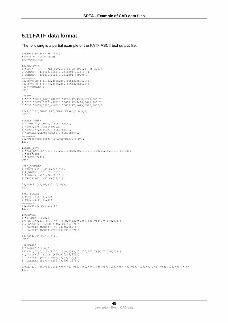
5.11 FATF data format
The following is a partial example of the FATF ASCII text output file. :FABMASTER FATF REV 11.0; :UNITS = 1/1000 INCH; :NOAUTOROTATE :BOARD_DATA 1,"JOB" ("E1_T1",1.0,14-05-2001,17-05-2001); 2,CONTOUR ((11513,3615,0),(11801,3615,0)); 3,CONTOUR ((11801,3615,0),(11801,490,0)); …………………… 32,CONTOUR ((11383,3505,0),(11513,3505,0)); 33,CONTOUR ((11513,3505,0),(11513,3615,0)); 34,FIDUCIALS(); :EOD :PARTS 1,"C1","10UF_10V_1206/2","1206/1",4330,3770,900,T; 2,"C2","100N_0603_Y5V/1","0603/1",4420,3645,900,T; 3,"C3","100N_0603_Y5V/1","0603/1",1645,3575,1800,T; …………………… 1247,"Z19","MTHOLE1","MTHOLE1AA",0,0,0,T; :EOD :LAYER_NAMES 1,"COMMON",COMMON,0,ELECTRICAL; 2,"TOP",TOP,3,ELECTRICAL; 3,"BOTTOM",BOTTOM,2,ELECTRICAL; 4,"INNER1",TRANSPARENT,2,ELECTRICAL; …………………… 34,"Probkeep.bot#1",TRANSPARENT,-1,DXF; :EOD :LAYER_SETS 1,"ALL_LAYERS",(1,2,3,4,5,6,7,8,9,10,11,12,13,14,15,16,17,18,19,20); 2,"TOP",(2); 3,"BOTTOM",(3); :EOD :PAD_SYMBOLS 1,TRACK (55,(-45,0)(45,0)); 2,P_BLOCK (-15,-15,15,15); 3,P_BLOCK (-20,-20,20,20); 4,TRACK (40,(-37,0)(37,0)); …………………… 34,TRACK (12,(0,-30)(0,30)); :EOD :PAD_STACKS 1,PST1,27,P,((1,1)); 2,PST2,15,P,((1,2)); …………………… 44,PST44,30,P,((1,9)); :EOD :PACKAGES 1,"14SMX",0,0,0,0 (PINS(1,"",0,0,T)(2,"",0,100,T)(3,"",250,100,T)(4,"",250,0,T)) (1, LAYER(2 (BLOCK (-45,-27,45,27))) 2, LAYER(2 (BLOCK (-45,73,45,127))) 3, LAYER(2 (BLOCK (205,73,295,127))) …………………… 44,PST44,30,P,((1,9)); :EOD :PACKAGES 1,"14SMX",0,0,0,0 (PINS(1,"",0,0,T)(2,"",0,100,T)(3,"",250,100,T)(4,"",250,0,T)) (1, LAYER(2 (BLOCK (-45,-27,45,27))) 2, LAYER(2 (BLOCK (-45,73,45,127))) 3, LAYER(2 (BLOCK (205,73,295,127))) …………………… TRACK (10,(50,-55),(46,-55),(43,-55),(40,-56),(38,-57),(35,-58),(32,-59),(29,-61),(27,-63),(25,-65))))); :EOD

SPEA - Example of CAD data files
46 Leonardo – Board CAD data
:NETS 1,"+3.3VA",S, ((177,3),(177,1),(177,5),(178,1),(177,7),(103,1),(178,3),(178,5),(178,7),(1228,8),(112,1),(113,1),(493,1),(481,2),(506,2),(114,1),(478,2),(1230,162),(1074,1),(463,2),(458,2),(440,2),(452,2),(91,1),(445,2),(83,1),(1230,133),(125,1),(1230,1),(1131,1),(1230,14),(130,1),(77,1),(92,1),(371,1),(367,2),(372,2),(382,2),(403,2),(405,2),(419,2),(397,1),(1230,117),(93,1),(426,2),(427,2),(1230,100),(1222,27),(71,1),(368,2),(60,1),(356,2),(348,2),(347,1),(322,2),(341,2),(59,1),(1222,3),(56,1),(311,2),(334,1),(310,2),(282,1),(283,1),(320,2),(330,1),(55,1),(318,1),(1224,75),(53,1),(165,1),(297,2),(290,1),(162,1),(169,1),(1224,93),(1224,71),(377,2),(402,2),(1224,91),(1224,92),(1224,124),(1224,130),(1224,164),(1224,177),(1224,182),(78,1),(79,1),(80,1),(173,1),(175,1),(404,2),(174,1),(1224,186),(172,1),(407,2),(411,2),(1224,66),(412,2),(72,1),(342,2),(357,2),(383,2),(85,1),(1210,4),(38,2),(39,2),(40,2),(41,2),(73,1),(1210,2),(656,1),(43,2),(42,2),(176,2),(191,1),(192,1),(193,1),(194,1),(74,1),(75,1),(57,1),(349,2),(323,2),(303,1),(362,2),(369,2),(62,1),(373,2),(378,2),(418,2),(424,2),(423,2),(417,2),(422,2),(416,2),(421,2),(415,2),(420,2),(414,2),(428,2),(429,2),(430,2),(431,2),(432,2),(89,1),(441,2),(1230,53),(1230,56),(1230,70),(97,1),(437,2),(1230,32),(1230,45),(131,1),(117,1),(126,1),(120,1),(1230,85),(811,1),(484,2),(514,2),(500,2),(499,2),(495,2),(490,2),(496,2),(487,2),(491,2),(482,2),(488,2),(483,2),(480,2),(476,2),(475,2),(470,2),(464,2),(471,2),(459,2),(465,2),(453,2),(460,2),(454,2),(1224,80),(24,1),(25,1),(36,1),(559,1),(258,1),(262,2),(12,1),(1209,20),(27,1),(261,2),(1224,176),(1224,165),(160,1),(161,1),(168,1),(1224,133),(1224,191),(26,1),(1224,128),(179,2),(33,1),(1213,14),(47,1),(312,2),(1,1)); 2,"+3.3VB",S, ((44,1),(1221,16),(557,1),(49,1),(20,1),(1221,132),(15,1),(21,1),(22,1),(63,1),(23,1),(1221,122),(158,1),(1221,192),(54,1),(1221,201),(88,1),(1221,157),(1221,159),(163,1),(166,1),(1221,2),(1221,78),(61,1),(68,1),(1221,96),(1221,118),(170,1),(171,1),(962,1),(98,1),(388,2),(413,2),(84,1),(1227,17),(1227,41),(101,1),(1227,9),(159,1),(1221,100),(167,1),(1221,59),(1221,61),(164,1),(389,2),(926,1),(111,1),(1229,4),(191,2),(192,2),(193,2),(194,2),(105,2),(108,2),(106,2),(1227,29),(1229,2),(973,1),(73,2),(74,2),(72,2),(75,2),(107,2),(109,2),(110,2),(122,1),(123,1),(1092,1),(104,1)); 3,"+5V",S, ((190,5),(180,5),(124,1),(136,1),(462,2),(1226,7),(439,2),(90,1),(100,2),(857,1),(946,1),(94,1),(446,2),(447,2),(1222,23),(256,2),(564,1),(3,1),(267,1),(6,1),(4,1),(1208,8),(210,2),(1225,6),(473,1),(99,2),(744,1),(51,1),(324,2),(455,2),(1212,16),(1214,16),(304,2),(1217,16),(313,2),(325,2),(456,2),(508,2),(1229,3),(110,1),(1219,5),(1220,5),(879,1),(76,1),(95,1),(115,1),(116,2),(379,2),(1218,5),(1215,5),(1216,5),(8,2),(39,1),(14,2),(1223,5),(364,2),(370,2),(38,1),(40,1),(41,1),(109,1),(108,1),(107,1),(1210,3),(952,1),(119,1),(338,2),(344,2),(345,2),(346,2),(359,2),(339,2),(265,2),(327,2),(328,2),(340,2),(315,2),(316,2),(317,2),(329,2),(307,2),(300,2),(308,2),(309,2),(301,2),(294,2),(296,2),(302,2),(278,2),(279,2),(280,2),(295,2),(273,2),(270,2),(274,2),(275,2),(352,2),(360,2),(365,2),(353,2),(354,2),(361,2),(565,1),(16,1),(237,2),(236,2),(238,2),(1211,5),(5,1),(182,1),(551,1),(211,2),(181,1),(45,1));4,"0V_A",S,((1176,1),(180,57),(133,1),(132,2),(184,1),(141,1));5,"2MSCLK_DSP1",S,((449,2),(186,3),(944,1)); …………………… 699,"\PORT_2MSCLK",S, ((391,1),(943,1),(1227,40)); :EOD :PADS 1,41,((1100,980),(1190,980),(2125,1108),(2290,770),(2355,895),(2440,950),(2265,280), (2590,810),(2440,1220),(2440,1330),(2440,1440),(2580,1565),(2575,1840),(2645,485), (2995,515),(2630,1985),(3005,1935),(3080,1840),(3090,1610),(2650,2160),(2650,2270), (2545,2275),(2650,2325),(2880,1935),(2205,2060),(3310,1565),(3300,1730),(3405,1720), (2045,2140),(2770,2425),(2645,2480),(2550,2540),(2645,2590),(2650,2700),(2465,2425), (2770,2645),(2365,2750),(2235,2915),(2180,2915),(2010,2710),(1875,2658),(1415,2730), (1250,2695)); 1,42,((2980,2879)); 1,41,((2770,2855),(2645,2800),(2645,2910)); …………………… 699,41,((10460,1525)); :EOD :LAYERS 1,LAYER (2 (TRACK (10,(18,745),(-82,745)))); 1,LAYER (2 (TRACK (10,(118,745),(18,745)))); 1,LAYER (2 (TRACK (10,(218,745),(118,745)))); …………………… 699,LAYER (2 (TRACK (5,(10460,1525),(10460,1245),(10390,1175),(10390,1165),(10360,1135),(10360,1065),(10360,1064), (10390,1034),(10444,1034)))); :EOD

SPEA - Example of CAD data files
47 Leonardo – Board CAD data
5.12 FABMASTER CAD data format
The following is a partial example of a FabMaster ASCII test output file. :BOARDINFO DEMOBOARD ,800020AB001,4000 ,3000 ,8400 ,6500 ,08/05/97,1.00 ,MILS,120 ,4 :ENDBOARDINFO :PARTLIST 0 ,R1 ,14544200AB02 ,4500 ,5400 ,T,180 0 ,D2 ,22001200AB04 ,6500 ,2400 ,T, 0 0 ,IC1 ,40008600AB02 ,7900 ,6000 ,T, 0 0 ,TP1 ,TEST_POINT ,6000 ,3400 ,B, 0 0 ,VIA1 ,VIA_100 ,6400 ,4000 ,B, 0 0 ,VIA2 ,VIA_100 ,6100 ,4000 ,B, 0 ……………… :ENDPARTLIST :PNDATA 14544200AB02 , 1, ,15 ,10 ,10 ,10 ,200 ,110 ,100 14544200AB04 , 1, ,15 ,0.470 ,20 ,20 ,200 ,110 ,100 22001200AB04 , 30,1N4148 ,15 , , , ,200 ,120 ,100 40008600AB02 ,200,74LS00 ,5 , , , ,800 ,300 ,150 TEST_POINT ,800, ,0 , , , ,50 ,50 ,0 VIA_100 ,802, ,0 , , , ,50 ,50 ,0 ……………… :ENDPNDATA :NETLIST 1 ,GND ,R1 ,1 ,4400 ,5400 ,N 2 ,VCC ,R1 ,2 ,4600 ,5400 ,N 1 ,GND ,D2 ,A ,6400 ,5400 ,N 3 ,NET_A ,D2 ,K ,6600 ,5400 ,N 3 ,NET_A ,R2 ,1 ,4400 ,5400 ,N 1 ,VCC ,IC1 ,14 ,7600 ,6150 ,B 2 ,GND ,IC1 ,7 ,8400 ,5850 ,B 4 ,NET_B ,IC1 ,1 ,7600 ,5850 ,B 3 ,NET_A ,IC1 ,2 ,7700 ,5850 ,B 5 ,NET_C ,IC1 ,3 ,7800 ,5400 ,B 6 ,$NC1 ,IC1 ,4 ,7900 ,5400 ,B 7 ,$NC2 ,IC1 ,5 ,8000 ,5400 ,B 8 ,$NC3 ,IC1 ,6 ,8100 ,5400 ,B 9 ,$NC4 ,IC1 ,7 ,8200 ,5400 ,B 9 ,$NC5 ,IC1 ,8 ,8200 ,6150 ,B 9 ,$NC6 ,IC1 ,9 ,8100 ,6150 ,B 9 ,$NC7 ,IC1 ,10 ,8000 ,6150 ,B 9 ,$NC8 ,IC1 ,11 ,7900 ,6150 ,B 9 ,$NC9 ,IC1 ,12 ,7800 ,6150 ,B 9 ,$NC10 ,IC1 ,13 ,7700 ,6150 ,B 2 ,VCC ,TP1 ,1 ,6000 ,3400 ,B 2 ,GND ,TP2 ,1 ,6800 ,4000 ,B 2 ,GND ,VIA2 ,1 ,6100 ,4000 ,A ……………… :ENDNETLIST :TESTPOINT 1 ,TP1-1 ,VCC ,TP1 ,1 ,M ,6 ,6000 ,3400 ,B 2 ,IC1-14 ,VCC ,IC1 ,14 ,K ,4 ,7600 ,6150 ,B 3 ,TP2-1 ,GND ,TP2 ,1 ,M ,6 ,6800 ,4000 ,B 4 ,VIA1-1 ,GND ,VIA1 ,1 ,K ,3 ,6400 ,4000 ,B 5 ,VIA2-1 ,GND ,VIA2 ,1 ,K ,3 ,6100 ,4000 ,B 6 ,IC1-4 ,$NC1 ,IC1 ,4 ,M ,4 ,7900 ,5400 ,B 8 ,IC1-6 ,$NC3 ,IC1 ,6 ,M ,4 ,8100 ,5400 ,B 9 ,IC1-7 ,$NC4 ,IC1 ,7 ,M ,4 ,8200 ,5400 ,B 10 ,IC1-8 ,$NC5 ,IC1 ,8 ,M ,4 ,8200 ,6150 ,B 11 ,IC1-9 ,$NC6 ,IC1 ,9 ,M ,4 ,8100 ,6150 ,B 12 ,IC1-10 ,$NC7 ,IC1 ,10 ,M ,4 ,8000 ,6150 ,B 14 ,IC1-12 ,$NC9 ,IC1 ,12 ,M ,4 ,7800 ,6150 ,B 15 ,IC1-13 ,$NC10 ,IC1 ,13 ,M ,4 ,7700 ,6150 ,B 16 ,IC1-2 ,NET_A ,IC1 ,2 ,M ,4 ,7700 ,5850 ,B 18 ,IC1-3 ,NET_C ,IC1 ,3 ,M ,4 ,7800 ,5400 ,B ……………… :ENDTESTPOINT

SPEA - Example of CAD data files
48 Leonardo – Board CAD data
5.13 GENCAD data format
The following is a partial example of a GENCAD ASCII text output file. $HEADER GENCAD 1.4 USER RSI-TRANSLATOR GENCAD OUTPUT V:16 DRAWING C:\TEMP\XTC\NEUTRAL_FILE_PCB REVISION Thu Jun 01 08:27:33 2000 UNITS USER 1000 ORIGIN 0 0 INTERTRACK 0 $ENDHEADER $BOARD LINE -730.500 -297.600 7639.600 -297.600 LINE 7639.600 -297.600 7639.600 6123.650 LINE 7639.600 6123.650 -730.500 6123.650 LINE -730.500 6123.650 -730.500 -297.600 $ENDBOARD $PADS PAD pad_0 RECTANGULAR -1 RECTANGLE -12.500 -17.500 25.000 35.000 PAD pad_1 RECTANGULAR -1 RECTANGLE -12.500 -25.000 25.000 50.000 PAD pad_2 RECTANGULAR -1 RECTANGLE -12.500 -30.000 25.000 60.000 PAD pad_3 RECTANGULAR -1 RECTANGLE -15.000 -7.000 30.000 14.000 ………………………… PAD pad_89 RECTANGULAR -1 RECTANGLE -25.000 -45.000 35.000 90.000 $ENDPADS $PADSTACKS PADSTACK s25x35 0.000 PAD pad_0 TOP 0 0 PADSTACK s25x50 0.000 PAD pad_1 TOP 0 0 ………………………… PAD pad_87 TOP 0 0 PADSTACK s35x90m7.5 0.000 PAD pad_88 TOP 0 0 PADSTACK s35x90p7.5 0.000 PAD pad_89 TOP 0 0 $ENDPADSTACKS $SHAPES SHAPE SO8 LINE -98.400 -122.000 98.400 -122.000 LINE 98.400 -122.000 98.400 122.000 LINE 98.400 122.000 -98.400 122.000 ………………………… INSERT TH SHAPE NONPLATED_HOLE_0.039 PIN 1 NONPLATED_HOLE_0.039 0.000 0.000 TOP 0 0 INSERT SMD $ENDSHAPES $COMPONENTS COMPONENT C1 DEVICE "C1_RJC5402057/44" PLACE -280.000 1030.000 LAYER TOP ROTATION 0 SHAPE cap6a 0 0 ATTRIBUTE COMPATTR_1 "REFLOC" "ML,63.0,103.0,0,BL,40.0,40.0,10.0,std,1" ………………………… COMPONENT R236 DEVICE "R236_REZ401055/1" PLACE 5905.000 3170.000 LAYER TOP ROTATION 0 SHAPE K0805HD 0 0 ATTRIBUTE COMPATTR_1 "REFLOC" "ML,-165.0,0.0,0,CC,30.0,30.0,10.0,std,1" COMPONENT R237 DEVICE "R237_REN60960/1" PLACE 5807.000 1200.000 LAYER TOP

SPEA - Example of CAD data files
49 Leonardo – Board CAD data
ROTATION 180 SHAPE K2717 0 0 ATTRIBUTE COMPATTR_1 "REFLOC" "ML,0.0,0.0,180,CC,30.0,30.0,10.0,std,1" ………………………… COMPONENT V110 DEVICE "V110_RYN1216068/1" PLACE 2400.000 3005.000 LAYER TOP
ROTATION 270 SHAPE SOT23B 0 0 ATTRIBUTE COMPATTR_1 "REFLOC" "ML,-4.4,-0.35,90,CC,30.0,30.0,10.0,std,1" COMPONENT V111 DEVICE "V111_RYN120614/1" PLACE 2460.000 2490.000 LAYER TOP ROTATION 270 SHAPE SOT23B 0 0 ATTRIBUTE COMPATTR_1 "REFLOC" "ML,-4.15,1.5,90,CC,30.0,30.0,10.0,std,1" ………………………… COMPONENT X101 DEVICE "X101_RPV403226/001" PLACE 885.700 621.700 LAYER TOP ROTATION 0 SHAPE 001_BYZ60611_9 0 0 ATTRIBUTE COMPATTR_1 "REFLOC" "ML,421.3,-191.7,0,CC,40.0,40.0,1.0,std,1" COMPONENT X201 DEVICE "X201_RNT403196/1" PLACE 7342.000 5570.500 LAYER TOP ROTATION 0 SHAPE tnc_50 0 0 COMPONENT V101 DEVICE "V101_RYN1216068/1" PLACE 2707.000 3125.000 LAYER TOP ROTATION 270 SHAPE SOT23B 0 0 ATTRIBUTE COMPATTR_1 "REFLOC" "ML,-5.15,-1.55,90,CC,30.0,30.0,10.0,std,1" ………………………… $ENDCOMPONENTS $DEVICES DEVICE "C1_RJC5402057/44" PART "RJC5402057/44" VALUE "4.4uF" TYPE "CAP" DESC "cap6a" PINDESC 1 1 PINDESC 2 2 PINDESC 3 3 DEVICE "C2_RJC5402057/44" PART "RJC5402057/44" VALUE "4.4uF" TYPE "CAP" DESC "cap6a" PINDESC 1 1 PINDESC 2 2 PINDESC 3 3 PINDESC 4 4 ………………………… DEVICE "R7_REP622655/1" PART "REP622655/1" VALUE "10k" TYPE "RES" DESC "K0402D" PINDESC 1 1 PINDESC 2 2 DEVICE "R8_REP622452/22" PART "REP622452/22" VALUE "22R" TYPE "RES" DESC "K0402D" PINDESC 1 1 PINDESC 2 2 DEVICE "T1_REG2542401" PART "REG2542401" TYPE "trans" DESC "finduct9" PINDESC 1 1 PINDESC 2 2 PINDESC 3 3

SPEA - Example of CAD data files
50 Leonardo – Board CAD data
…………………………
5.13.1 REMARK
The GenCad CAD-CAE runs under Unix operating system and generates its neutral ASCII output file in Unix format. The Unix ASCII text files use as end of line identifier, the ASCII character "0ahex". The Windows operating system uses for ASCII text files, as end of line identifier, the ASCII characters "0dhex" and "0ahex". This means that output ASCII text files may require an ASCII format conversion (from Unix to Windows format). This operation can be performed using "WordPad". Open the GenCad ASCII file with this editor and save it; this operation will automatically perform the conversion from ASCII Unix format to ASCII Windows format.

SPEA - Example of CAD data files
51 Leonardo – Board CAD data
5.14 IPC –D- 356 data format
The following is a partial example of a IPC – 356 –D FabMaster ASCII test output file. P JOB C:\JIVAROS-PILOT(20400046_A0)\20400046_A0\20400046_A0.brd 00000 P FORM F 00001 P CODE 00 00002 P DIM N 00003 P UNITS CUST 00004 P TITLE C:\JIVAROS-PILOT(20400046_A0)\20400046_A0\20400046_A0.brd 00005 P NUM 001 00006 P REV A 00007 C 00008 C 00009 C IPC-D-356 Ouptut File from Allegro 00010 C IPC File Date: Mon Jun 16 16:38:51 2003 00011 C Login Name: laszlo 00012 C 00013 C 00014 C Board File: C:\JIVAROS-PILOT(20400046_A0)\20400046_A0\20400046_A0.brd00015 C Extract File Date: Mon Jun 16 16:37:59 2003 00016 C Design Rule Status: UP TO DATE 00017 C Unit of Measure: mils 00018 C Decimal Place Accuracy: 2 00019 C Number of etch Layers: 14 00020 C Board Thickness(mils): 118.60 00021 C Drawing Extents(mils): -75000 -73340 425000 426660 00022 C 00023 C BOARD LAYER INFORMATION 00024 C 00025 C Layer Layer Layer Layer 00026 C Name Material Thickness Type No 00027 C ------------------------------------------ 00028 C TOP COPPER 14 COND POS 2 1 00029 C BOTTOM COPPER 14 COND POS 28 14 00042 C 00043 C PADSTACK INFORMATION 00044 C 00045 C Padstack First Last 00046 C Name Layer Layer Width Length Shape Count 00047 C ---------------------------------------------------------- 00048 C S43X39 TOP TOP 390 430 RECT 24 00049 C C100P68 TOP BOTTOM 1250 1250 CIRCLE 20 00050 C FIDUCIAL40 TOP TOP 1300 1300 CIRCLE 8 00121 C 00122 C VIA INFORMATION 00123 C 00124 C Via First Last 00125 C Name Layer Layer Width Length Shape Count 00126 C ---------------------------------------------------------- 00127 C VIATEST TOP BOTTOM 370 370 CIRCLE 157 00128 C VIA TOP BOTTOM 350 350 CIRCLE 2308 00131 C 00138 C DRILL INFORMATION 00139 C 00140 C Drill 00141 C Size Plating 00142 C -------------------- 00143 C 680.00 PLATED 00144 C 9843.00 UNPLATED 00168 C 00169 C ************************************* 00228 C Board Layer to Data Layer Mapping 00229 C ************************************* 00230 C 00231 P LAYER 01 COMP 01 02 03 00232 P LAYER 02 COMP 04 05 06 00233 C 00246 P AREA 1 X- 75000Y- 73340X+ 425000Y+ 426660 00247 C 00248 C ************************************* 00249 C SIGNAL PINS ON THE BOARD 00250 C ************************************* 00251 C 00252 32712N526 C8 -1 A14X+008400Y+024500X0350Y0270R090 S2 3279N598 U11 -A4 A01X+073400Y+029510X0260Y0260 S1 3279N600 R241 -1 A01X-001665Y+034750X0440Y0390 S1 3279N600 U11 -B20 A01X+072900Y+021510X0260Y0260 S1 3279N605 R194 -2 M A01X-002335Y+034000X0440Y0390 S1 3179N605 DS1 -1 D0400PA00X-008780Y+035917X0600Y0600 S3 3279N624 R111 -1 A14X+074415Y+029650X0440Y0390 S2 3279N624 U11 -C6 A01X+072400Y+028510X0260Y0260 S1

SPEA - Example of CAD data files
52 Leonardo – Board CAD data
3279N626 R112 -1 A14X+074415Y+027150X0440Y0390 S2 317GND VIA - MD0080PA00X+066650Y+025760 S0 C 00271 C 00272 C ************************************* 00273 C NET NAMES USED 00274 C ************************************* 00275 C 00276 P NNAME10000 AC_FROM_EXTCH0_N 00277 P NNAME10001 AC_FROM_EXTCH0_P 00278 P NNAME10002 DELAY_OTHER_CARD_N 00279 P NNAME10003 DRIVE10_MATED_N 00280 P NNAME10004 DRIVE11_MATED_N 00281 P NNAME10005 DRIVE12_MATED_N 00282 P NNAME10006 DRIVE13_MATED_N 00283 P NNAME10007 DRIVE14_MATED_N 00284 P NNAME10008 DRIVE15_MATED_N 00285 P NNAME10009 MEM_VALID_LATCH 00286 P NNAME10010 OTHER_IO_MASTER 00287 P NNAME10011 OTHER_IO_PRESENT_N 00288 P NNAME10012 UNUSED_DRIVE_SEL3 00289 C 00290 999 00291

SPEA - Example of CAD data files
53 Leonardo – Board CAD data
5.15 MENTOR CAD data format
The following is a partial example of a Mentor ASCII text output file. ############################################# ###Board Information ############################################# BOARD C280-A35-B11-6-6 OFFSET x:0.0 y:0.0 ORIENTATION 0 B_UNITS Mm ############################################# ###Attribute Information ############################################# B_ATTR 'MILLING_ORIGIN' 'MILLING 0 0.0 0' 0.0 0.0 B_ATTR 'DRILL_ORIGIN' '' 0.0 0.0 B_ATTR 'BOARD_DEFINITION_IDENTIFIER' '' B_ATTR 'BOARD_THICKNESS' '' 1.6 B_ATTR 'BOARD_INTERNAL_COPPER' '' 0.0 ………. ############################################# ###Nets Information ############################################# NET -5VN_PIN D509-12 -77.47 -103.505 so_r 1 N_PIN D562-2 -150.8125 -114.3 so_l 1 N_VIA -76.67625 -112.7125 via_025 1 24 N_VIA -150.8125 -117.475 via_025 1 24 N_PIN D562-6 -155.8925 -114.3 so_l 1 N_PIN D509-11 -78.74 -103.505 so_r 1 N_VIA -78.105 -113.03 via_025 1 24 N_VIA -155.8925 -115.72875 via_025 1 24 N_VIA -59.69 -110.01375 via_025 1 24 N_VIA -63.02375 -117.1575 via_025 1 24 N_VIA -70.32625 -118.11 via_025 1 24 N_PIN D98-11 -152.0825 -94.2975 so_r 1 N_PIN D98-10 -150.8125 -94.2975 so_r 1 ……….. ############################################# ###Geometry Information ############################################# GEOM b_dils4_076 G_PIN 1 -4.445 1.27 b_dils4_076_l Surf G_PIN 2 -4.445 -1.27 b_dils4_076_l Surf G_PIN 3 4.445 -1.27 b_dils4_076_r Surf G_PIN 4 4.445 1.27 b_dils4_076_r Surf G_ATTR 'COMPONENT_HEIGHT' '' 5.1 0.0 G_ATTR 'COMPONENT_OUTLINE_OVERHANG' 'no' G_ATTR 'COMPONENT_LAYOUT_SURFACE' 'both' G_ATTR 'COMPONENT_LAYOUT_TYPE' 'surface' G_ATTR 'COMPONENT_INSERT_TYPE' 'smd' G_ATTR 'COMPONENT_DEFAULT_PADSTACK' 'b_dils4_076_l' GEOM cd150_050_180_n100 ……………. ############################################# ###Component Information ############################################# COMP B130 V4044-Z6357-S2 QUARZ gq050_130_050_smt -139.54125 -78.4225 1 0 C_PROP (VALUE,"3.579545MHz") (MULTI_ASSY,"all,c1,c2") (REFLOC,"MM,-0.9525,-1.5 C_PIN B130-1 -141.76375 -73.66 1 1 0 gq050_130_050_smt_tl /N$510 C_PIN B130-2 -141.76375 -83.185 1 1 0 gq050_130_050_smt_bl /_NF$14 C_PIN B130-3 -137.31875 -83.185 1 1 0 gq050_130_050_smt_br /_NF$13 COMP B300 V3708-Z16-X47 OPTO_CPL b_dils4_076 -234.315 -100.0125 1 270 C_PROP (VALUE,"SFH6106T-4") (MULTI_ASSY,"all,c1,c2") (REFLOC,"MM,-0.635,-1.905 C_PIN B300-1 -233.045 -95.5675 1 1 270 b_dils4_076_l /N$31884 C_PIN B300-2 -235.585 -95.5675 1 1 270 b_dils4_076_l /N$881 C_PIN B300-4 -233.045 -104.4575 1 1 270 b_dils4_076_r /N$926 COMP B400 V3708-Z16-X12 OPTO_CPL b_dils4_076 -162.56 -172.085 1 0 C_PROP (VALUE,"SFH6106-2") (MULTI_ASSY,"all,c1,c2") (REFLOC,"MM,-0.635,-1.905, C_PIN B400-2 -167.005 -173.355 1 1 0 b_dils4_076_l /N$737 ………..

SPEA - Example of CAD data files
54 Leonardo – Board CAD data
5.15.1 REMARK
The Mentor CAD-CAE runs under Unix operating system and generates its neutral ASCII output file in Unix format. The Unix ASCII text files use as end of line identifier, the ASCII character "0ahex". The Windows (MS-DOS) operating system uses for ASCII text files, as end of line identifier, the ASCII characters "0dhex" and "0ahex". This means that output ASCII text files may require an ASCII format conversion (from Unix to Windows format). This operation can be performed using "WordPad". Open the .Mentor ASCII file with this editor and save it; this operation will automatically perform the conversion from ASCII Unix format to ASCII Windows format.

SPEA - Example of CAD data files
55 Leonardo – Board CAD data
5.16 ORCAD LAYOUT data format
The following is a partial example of the OrCad ASCII text output file. (MIN (Version 9100) (MajorRev 9)(MinorRev 1) (L 28)(V 16) (Begin (Header (Grid 300) (ViaGrid 300) (UserDiv 60) (DisplayGrid 0) (PlaceGrid 1500 1500) (DetailGrid 300 300) (DotGrid 1500 1500) (DisplayPrecision 60) (Origin 0 36000) (InchFactor 0.00001666666666666667) (View 82848 108150 251136 314820) (OffGrid)(MultiVia Off)(Metric Off)(ConnectThruPours) (BackupSweep)(BackupInterval 10)(TimeUsed 65696509) (RotateAngle 5400) (AngleSnap 1) (PinTestPoints Off) (DrlChartLoc -19200 -2400) (DrlChartTextHeight 6000) (DrlChartLineWidth 600) (DrillSize (Diam 1200)(Symbol 143)) …………………… (MaxDistance 18000) ) (Strat 0(N "Win/Comp/Manual") (Diag Max) (Dir NEXT UP NEXT NEXT) (Pass 0(Enabled)(Done Off)(Maze) (Nearest Off)(Partial)(Fast Off)(Via 60)(Retry 60)(Limit 100) (Attempts 2)) (Pass 1(Enabled)(Done Off)(Heur) (Nearest Off)(Partial Off)(Fast Off)(Via 0)(Retry 0)(Limit 0) (Attempts 2)) (Pass 2(Enabled)(Done Off)(Maze) (Nearest Off)(Partial)(Fast Off)(Via 70)(Retry 30)(Limit 80) (Attempts 20)) (Pass 3(Enabled Off)(Done Off)(Maze) (Nearest Off)(Partial)(Fast Off)(Via 40)(Retry 60)(Limit 80) (Attempts 20)) (Pass 4(Enabled Off)(Done Off)(Maze) (Nearest Off)(Partial Off)(Fast Off)(Via 75)(Retry 100) (Limit 75)(Attempts 3)) (L 1(Enabled)(Dir 80)(Cost 50)(BottleNeck 30)) (L 2(Enabled)(Dir 20)(Cost 50)(BottleNeck 30)) (L 3(Enabled Off)(Dir 20)(Cost 50)(BottleNeck 30)) …………………… (THRU 52(N "SM.llb_pad11")(Uid -1141)(TestPt Off)(NonPlated Off) (LgThermal Off)(DirectHit Off) (L 1(Rect 5100 1200 5100 1200)(R 5400)) (L 2(UNDEF)(R 5400)) (L 3(UNDEF)(R 5400)) (L 4(UNDEF)(R 5400)) (L 5(UNDEF)(R 5400)) (L 6(UNDEF)(R 5400)) (L 7(UNDEF)(R 5400)) (L 8(UNDEF)(R 5400)) (L 9(UNDEF)(R 5400)) (L 10(UNDEF)(R 5400)) (L 11(UNDEF)(R 5400)) (L 12(UNDEF)(R 5400)) (L 13(UNDEF)(R 5400)) (L 14(UNDEF)(R 5400)) (L 15(UNDEF)(R 5400)) (L 16(UNDEF)(R 5400)) (L 17(Rect 5100 1200 5100 1200)(R 5400)) (L 18(UNDEF)(R 5400)) (L 19(Rect 5100 1200 5100 1200)(R 5400)) (L 20(UNDEF)(R 5400)) (L 21(UNDEF)(R 5400)) (L 22(UNDEF)(R 5400)) (L 23(Rect 5100 1200 5100 1200)(R 5400))

SPEA - Example of CAD data files
56 Leonardo – Board CAD data
5.17 PADS CAD data format
The following is a partial example of a ASCII text output file. !PADS-POWERPCB-V3.5-MILS! DESIGN DATABASE ASCII FILE 1.0 *PCB* GENERAL PARAMETERS OF THE PCB DESIGN UNITS 0 2=Inches 1=Metric 0=Mils USERGRID 5 Space between USER grid points MAXIMUMLAYER 2 Maximum routing layer WORKLEVEL 2 Level items will be created on DISPLAYLEVEL 1 toggle for displaying working level last LAYERPAIR 1 2 Layer pair used to route connection VIAMODE A Type of via to use when routing between layers LINEWIDTH 12 Width items will be created with TEXTSIZE 80 10 Height and LineWidth text will be created with JOBTIME 45932 Amount of time spent on this PCB design DOTGRID 1000 Space between graphic dots SCALE 8.391 Scale of window expansion ORIGIN 2800.29 452.09 User defined origin location WINDOWCENTER 6487.5 5602.5 Point defining the center of the window BACKUPTIME 2 Number of minutes between database backups REAL WIDTH 5 Widths greater then this are displayed real size ALLSIGONOFF 1 All signal nets displayed on/off REFNAMESIZE 70 4 Height and LineWidth used by part ref. names JOBNAME 006_100_089_03.pcb *REMARK* Colors 0-16 for levels 1-30 LINCOL 7 9 0 0 0 0 0 0 0 0 0 0 0 0 0 0 0 0 14 5 7 6 4 8 0 14 0 10 2 0 TXTCOL 5 9 0 0 0 0 0 0 0 0 0 0 0 0 0 0 0 0 1 5 7 6 4 8 0 14 0 10 2 0 TRKCOL 5 13 0 0 0 0 0 0 0 0 0 0 0 0 0 0 0 0 0 0 0 0 0 0 0 0 0 0 0 0 COPCOL 11 6 0 0 0 0 0 0 0 0 0 0 0 0 0 0 0 0 0 5 7 6 4 8 0 14 0 4 2 0 PADCOL 7 9 0 0 0 0 0 0 0 0 0 0 0 0 0 0 0 0 0 0 0 0 0 0 0 0 0 0 0 0 VIACOL 11 11 0 0 0 0 0 0 0 0 0 0 0 0 0 0 0 0 0 0 0 0 0 0 0 0 0 0 0 0 ERRCOL 3 3 0 0 0 0 0 0 0 0 0 0 0 0 0 0 0 0 0 0 0 0 0 0 0 0 0 0 0 0 CMTCOL 1 0 0 0 0 0 0 0 0 0 0 0 0 0 0 0 0 0 0 0 0 0 0 0 0 0 0 0 0 0 CMBCOL 0 14 0 0 0 0 0 0 0 0 0 0 0 0 0 0 0 0 0 0 0 0 0 0 0 0 0 0 0 0 RFDCOL 1 1 0 0 0 0 0 0 0 0 0 0 0 0 0 0 0 0 0 0 0 0 0 0 0 0 0 0 0 0 PRTCOL 0 0 0 0 0 0 0 0 0 0 0 0 0 0 0 0 0 0 0 0 0 0 0 0 0 0 0 0 0 0 LABCOL 0 0 0 0 0 0 0 0 0 0 0 0 0 0 0 0 0 0 0 0 0 0 0 0 0 0 0 0 0 0 KPTCOL 15 15 0 0 0 0 0 0 0 0 0 0 0 0 0 0 0 0 0 0 0 0 0 0 0 0 0 0 0 0 CONCOL 3 FBGCOL 4 0 HATCHGRID 25 Copper pour hatching grid TEARDROP 2713690 Teardrop tracks THERLINEWID 25 Copper pour thermal line width ……………… TEARDROPDATA 90 90 *REUSE* *REMARK* TYPE TYPENAME *REMARK* TIMESTAMP SECONDS *REMARK* PART NAMING PARTNAMING *REMARK* PART NAME *REMARK* NET NAMING NETNAMING *REMARK* NET MERGE NAME *REMARK* REUSE INSTANCENM PARTNAMING NETNAMING X Y ORI GLUED *TEXT* FREE TEXT *REMARK* XLOC YLOC ORI LEVEL HEIGHT WIDTH MIRRORED HJUST VJUST .REUSE. INSTANCENM 2520 4525 0.000 1 80 10 N LEFT DOWN 006.100.089.03 4475 3025 0.000 2 80 10 M LEFT DOWN LS 4400 3025 0.000 1 80 10 N LEFT DOWN BS 2480 4700 0.000 1 80 10 N LEFT DOWN 006.270.043.03 2849.71 997.91 0.000 22 120 10 N LEFT DOWN SMD ABDECKMASKE LS 4374.71 997.91 0.000 22 120 10 N LEFT DOWN EDELSTAHL 0,2mm 4375 250 0.000 0 120 10 N LEFT DOWN Pk 3224.71 3272.91 0.000 20 80 8 N LEFT DOWN TP1 2515 3625 0.000 20 80 8 N LEFT DOWN TP2 2699.71 3597.91 0.000 20 80 8 N LEFT DOWN TP3 2515 3415 0.000 20 80 8 N LEFT DOWN

SPEA - Example of CAD data files
57 Leonardo – Board CAD data
TP4 2699.71 3497.91 0.000 20 80 8 N LEFT DOWN ………………
*LINES* LINES ITEMS *REMARK* NAME TYPE XLOC YLOC PIECES TEXT SIGSTR *REMARK* .REUSE. INSTANCE RSIGNAL *REMARK* PIECETYPE CORNERS WIDTHHGHT LEVEL RESTRICTIONS *REMARK* XLOC YLOC BEGINANGLE DELTAANGLE *REMARK* XLOC YLOC ORI LEVEL HEIGHT WIDTH MIRRORED HJUST VJUST COP71129 COPPER -1800.29 547.91 1 COPCLS 9 50 4 2975 5500 2975 5150 3250 5150 3250 5225 3350 5225 3350 5425 3250 5425 3250 5500 2975 5500 COP72156 COPPER -1800.29 547.91 1 COPCLS 9 50 4 3650 5500 3650 5425 3550 5425 3550 5225 3650 5225 3650 5150 3925 5150 3925 5500 3650 5500 ……………… DRW67160007 LINES 2525 3050 2 OPEN 2 10 2 0 0 0 -75 OPEN 2 10 2 -35 -35 30 -35 *CLUSTER* ITEMS *REMARK* NAME XLOC YLOC PARENTID CLUSTERID CHILD_NUM ATTRIBUTE ATT2 BROID *VIA* ITEMS *REMARK* NAME DRILL STACKLINES [DRILL START] [DRILL END] *REMARK* LEVEL SIZE SHAPE [INNER DIAMETER] JMPVIA_AAAAA 37 3 -2 55 R -1 70 R 0 55 R STANDARDVIA 32 3 -2 50 R -1 50 R 0 50 R MICROVIA 20 3 -2 36 R -1 36 R 0 36 R DRW67160007 LINES 2525 3050 2 OPEN 2 10 2 0 0 0 -75 OPEN 2 10 2 -35 -35 30 -35 *CLUSTER* ITEMS *REMARK* NAME XLOC YLOC PARENTID CLUSTERID CHILD_NUM ATTRIBUTE ATT2 BROID *VIA* ITEMS *REMARK* NAME DRILL STACKLINES [DRILL START] [DRILL END] *REMARK* LEVEL SIZE SHAPE [INNER DIAMETER] JMPVIA_AAAAA 37 3 -2 55 R -1 70 R 0 55 R

SPEA - Example of CAD data files
58 Leonardo – Board CAD data
STANDARDVIA 32 3 -2 50 R -1 50 R 0 50 R MICROVIA 20 3 -2 36 R -1 36 R 0 36 R SOT23 I 380 610 1 3 1 0 2 CLOSED 5 6 0 -100 -20 20 -20
20 100 -100 100 -100 -20 VALUE -100 -150 0.000 1 70 4 N LEFT DOWN Part Type VALUE -100 -80 0.000 1 70 4 N LEFT DOWN Ref.Des. T0 0 0 0 T-80 0 -80 0 T-40 80 -40 80 PAD 0 3 -2 24 RF 90.000 30 0 0 -1 0 R 0 0 R ……………… *PARTTYPE* ITEMS *REMARK* NAME DECALNM UNITS TYPE GATES SIGPINS PINNMS FLAGS ECO *REMARK* G/S SWAPTYPE PINS *REMARK* PIN.SWAPTYPE.PINTYPE.FUNCNAME *REMARK* SIGPIN PIN WIDTH SIGNAME D-DLL4148 MINIMELF I DIO 1 0 2 0 Y G 1 2 1.0.U 2.0.U K A X2402SMD SO08 I ANA 1 2 0 0 Y G 0 6 1.0.L 2.0.L 3.0.L 5.0.S 6.0.S 7.0.S SIGPIN 8 60 +5V SIGPIN 4 60 GND MICS-D4 MICS-D4 I CON 1 0 0 1 Y G 0 4 1.1.U 2.1.U 3.1.U 4.1.U ……………… *PART* ITEMS *REMARK* REFNM PTYPENM X Y ORI GLUE MIRROR ALT CLSTID CLSTATTR BROTHERID LABELS *REMARK* .REUSE. INSTANCE RPART *REMARK* VISIBLE XLOC YLOC ORI HEIGTH WIDTH LEVEL MIRRORED HJUST VJUST RIGHTREADING IC10 X2402SMD 3470 6960 0.000 U N 0 -1 0 -1 2 VALUE 100 120 180.000 1 70 4 N LEFT DOWN Part Type VALUE 30 90 0.000 1 70 6 N LEFT DOWN Ref.Des. ……… R108 SMD-0805-10K 3295 5615 180.000 U N 0 -1 0 -1 2 VALUE 175 -55 180.000 1 70 6 N LEFT DOWN Ref.Des. VALUE 95 -125 90.000 1 70 4 N LEFT DOWN Part Type R109 SMD-0805-750K 3295 5765 180.000 U N 0 -1 0 -1 2 VALUE 25 -125 180.000 1 70 6 N LEFT DOWN Ref.Des. VALUE 95 -125 90.000 1 70 4 N LEFT DOWN *ROUTE* *REMARK* *SIGNAL* SIGNAME SIGFLAG COLOR *REMARK* REFNM.PIN .REUSE. INSTANCE RSIG REFNM.PIN .REUSE. INSTANCE RSIG *REMARK* XLOC YLOC LAYER SEGMENTWIDTH FLAGS [ARCDIR/VIANAME] [TEARDROP [P WID LEN [FLAGS]] [N WID LEN [FLAGS]]] [JMPNM JMPFLAG] REUSE INST RSIG *SIGNAL* GND 262657 -2 IC10.4 IC10.3 3620 6960 1 20 1024 TEARDROP N 90 90 3570 6960 31 20 512 TEARDROP P 90 90 ST3.10 IC10.4

SPEA - Example of CAD data files
59 Leonardo – Board CAD data
2674.71 7172.91 2 20 1024 TEARDROP N 90 90 2675 7285 2 20 1536 3590 7285 2 20 256 THERMAL TEARDROP P 90 90 N 90 90 3725 7150 2 20 1536 ……………… 3985 6785 1 40 320 MICROVIA THERMAL TEARDROP P 90 90 N 90 90 3760 6785 1 40 1600 3725 6820 1 40 1600 3725 6920 1 40 256 THERMAL TEARDROP P 90 90 N 90 90 ……………… *SIGNAL* GND 262657 -2 Q1.3 IC8.22 3875 6920 1 40 1280 THERMAL TEARDROP N 90 90 4005 6920 2 20 320 MICROVIA THERMAL TEARDROP P 90 90 N 90 90 4060 6920 2 20 1600 4065 6915 2 20 1600 4125 6915 1 20 320 MICROVIA THERMAL TEARDROP P 90 90 N 90 90 4125 6955 1 20 1600 4140 6970 1 20 1600 4200 6970 31 20 768 THERMAL TEARDROP P 90 90 *SIGNAL* GND 262657 -2 IC1.3 IC1.4 4090 6030 1 20 1280 THERMAL TEARDROP N 90 90 ……………… 4200 6870 31 12 768 THERMAL TEARDROP P 90 90 *POUR* POUR ITEMS *REMARK* NAME TYPE XLOC YLOC PIECES FLAGS [OWNERNAME SIGNAME HATCHGRID HATCHRAD] *REMARK* PIECETYPE CORNERS ARCS WIDTH LEVEL *REMARK* XLOC YLOC BEGINANGLE DELTAANGLE HP153 POUROUT 2424.71 4572.91 1 0 HP153 AGND POLY 13 0 25 2 -124.71 650 75 -1262.91 2445.29 -1262.91 2665.29 792.09 2690.29 1357.09 1645.29 1357.09 1645.29 2042.09 1165.31 2042.09 1165.31 2250.76 0.29 2254.3 0.29 1877.09 -124.71 1877.09 -124.71 650 ANP000000 HATOUT 25199.71 27547.91 1 0 HP153 POLY 597 447 25 2 ……………… *TESTPOINT* *REMARK* TEST POINTS ON COMPONENT PINS *REMARK* PIN XLOC YLOC SIDE SIGNAME REFDES.PIN PIN 2274.71 7072.91 0 +5V ST3.1 PIN 2599.71 3597.91 0 +5VG ST6.4 PIN 2274.71 7172.91 0 +12V ST3.2 PIN 2699.71 3597.91 0 AGND ST6.3 PIN 3224.71 3272.91 0 GND O10.1 PIN 2674.71 7172.91 0 GND ST3.10 PIN 2474.71 7072.91 0 I_X ST3.5 PIN 2474.71 7172.91 0 S_X ST3.6 ……………… *REMARK* TEST POINTS ON VIAS *REMARK* VIA XLOC YLOC SIDE SIGNAME SYMBOLNAME VIA 3860 4540 0 +2.5V MICROVIA VIA 4045 6340 0 +5V MICROVIA VIA 2515 5330 0 -12V MICROVIA VIA 3475 4565 0 1.25V MICROVIA ……………… *MISC* MISCELLANEOUS PARAMETERS *REMARK* PARENT_KEYWORD PARENT_VALUE *REMARK* [ { *REMARK* CHILD_KEYWORD CHILD_VALUE *REMARK* [ CHILD_KEYWORD CHILD_VALUE *REMARK* [ { *REMARK* GRAND_CHILD_KEYWORD GRAND_CHILD_VALUE [...] *REMARK* } ]] *REMARK* } ] POLAR_GRID...... 1 {

SPEA - Example of CAD data files
60 Leonardo – Board CAD data
X............... -960120000.000000 Y............... -1049655000.000000 RADIAL_STEP..... 7620000 ANGULAR_STEP.... 27000000 ORIENTATION..... 0 ……………… } DFT_CONFIGURATION PARENT { UNITS MILS PROBING_STRATEGY PARENT { PROBE_TOP_SIDE NO PROBE_VIAS YES PROBE_NO_CONNECT NO } DFT_RULES PARENT { PROBE 100 { DRILL_SIZE 69 ENABLE YES } PROBE 75 { DRILL_SIZE 43 ENABLE NO } PROBE 50 {
DRILL_SIZE 30 ENABLE NO } MIN_VIA_SIZE 25 MIN_PAD_SIZE 25 PIN_TO_PIN 14 PIN_TO_BOARD 125 PIN_TO_COMPONENT 0 } DIF_FILE PARENT { VIA_PREFIX VIA TP_PART_TYPE TP100 TP_PART_TYPE TP150 TP_PREFIX TP TP_PREFIX PN_TP ……………… } *MISC* MISCELLANEOUS PARAMETERS *REMARK* PARENT_KEYWORD PARENT_VALUE *REMARK* [ { *REMARK* CHILD_KEYWORD CHILD_VALUE *REMARK* [ CHILD_KEYWORD CHILD_VALUE *REMARK* [ { *REMARK* GRAND_CHILD_KEYWORD GRAND_CHILD_VALUE [...] *REMARK* } ]] *REMARK* } ] RULES_SECTION MILS { NET_CLASS DATA GROUP DATA DESIGN RULES { RULE_SET (1) { FOR : { DEFAULT : } AGAINST : { DEFAULT : } LAYER 0 CLEARANCE_RULE : { TRACK_TO_TRACK 12 VIA_TO_TRACK 12 ……………… *MISC* MISCELLANEOUS PARAMETERS

SPEA - Example of CAD data files
61 Leonardo – Board CAD data
*REMARK* PARENT_KEYWORD PARENT_VALUE *REMARK* [ { *REMARK* CHILD_KEYWORD CHILD_VALUE *REMARK* [ CHILD_KEYWORD CHILD_VALUE *REMARK* [ { *REMARK* GRAND_CHILD_KEYWORD GRAND_CHILD_VALUE [...] *REMARK* } ]] *REMARK* } ] CAM_SECTION PARENT { CAM_VERSION V3.0 CAM_DOC_LIST PARENT { CAM_DOC_DIRECTORY 006-100-089-03 CAM_DOC_NAME Drill Drawing { DOC_PLOT_TYPE Drill_Drawing DOC_DEVICE_TYPE Printer DOC_OUTPUT_FILE dd0124.lpr DOC_LAYER_NAMES Top Drill_Drawing DOC_LAYER_NUMBERS 1 24 0 0 DOC_LAYER_TYPES Component Routing DOC_SCALE 1 1 DOC_ORIENTATION 0 DOC_MIRROR N ……………… } *MISC* MISCELLANEOUS PARAMETERS *REMARK* PARENT_KEYWORD PARENT_VALUE *REMARK* [ { *REMARK* CHILD_KEYWORD CHILD_VALUE *REMARK* [ CHILD_KEYWORD CHILD_VALUE *REMARK* [ { *REMARK* GRAND_CHILD_KEYWORD GRAND_CHILD_VALUE [...] *REMARK* } ]] *REMARK* } ]
*MISC* MISCELLANEOUS PARAMETERS ATTRIBUTES DICTIONARY { ATTRIBUTE Value { TYPE FREETEXT N INHERITANCE PART PARTTYPE ECO_REGISTRATION Y READONLY N ……………… PART R47 { BEZEICHNUNG SMD Chip-Widerstand EDV-NUMMER 000.712.219 WERT 47K5 BAUFORM 1206 LIEFERANT#1 Rutronik Roederstein BEST-NR RMC1/8 47K5 1%1206RO D25 47K5 1% 1206FCS PREIS ……………… } PCB DEFAULT { DFT."Probe to Trace Clearance" 6.00mil DFT."Probe to Pad Clearance" 6.00mil DFT."Generate Test Points" No DFT."Allow Stubs" Yes DFT."Stub Length" 150.00mil DFT."Use Via Grid" Yes DFT."Grid X-Coordinate" 5.00mil DFT."Grid Y-Coordinate" 5.00mil } } *END* OF ASCII OUTPUT FILE

SPEA - Example of CAD data files
62 Leonardo – Board CAD data
5.17.1 REMARK
Pay attention to the fact that the PADS file must contains in its first row the word “MILS” that indicates that the used measure unit are inches. !PADS-POWERPCB-V3.5-MILS! DESIGN DATABASE ASCII FILE 1.0 Sometime the output text file can be generated using millimeter as measure units, in this case this line is equal to the one present below ans the import driver doesn’t work. !PADS-POWERPCB-V3.5-BASIC! DESIGN DATABASE ASCII FILE 1.0

SPEA - Example of CAD data files
63 Leonardo – Board CAD data
5.18 PCAD CAD data format
The following is a partial example of a PCAD ASCII text output file. %********************************************************************* % Program : PDIF-OUT VERSION 8.5 * % Format : P-CAD DATABASE INTERCHANGE FORMAT * %********************************************************************* {I so16l.prt IC1 {CN XN00015 XN00224 VCC 5.1V ? GND ? AA1 XN00102 CLK XN00004 ? VCC ? XN00222 GND} {ATR {IN {Pl 4600.00 3548.00} {Ro 1} [Ly "REFDTP"] [Ts 50.00][Tj "CC"][Tr 1][Tm "N"] {Nl 0.00 0.00} } {I r0805.prt R100B {CN VCC LNK1} {ATR {IN {Pl 5300.00 6254.00} {Ro 1} {Ps "B"} [Ly "REFDTP"] [Ts 50.00][Tj "CC"][Tr 0][Tm "N"] {Nl -155.00 -2.00} } % Component Name = so16l.prt. {COMP_DEF so16l.prt {PIN_DEF [Ly "PIN"] {P 1 {Pt 25}{Lq 0}{Ploc -150.00 175.00}} {P 2 {Pt 25}{Lq 0}{Ploc -150.00 125.00}} …………… {PIC [Ly "SLKTOP"] [Ls "SOLID"][Wd 8.00] [Ts 50.00][Tj "CC"][Tr 1][Tm "N"] {L -120.00 -215.00 120.00 -215.00 120.00 215.00 -120.00 215.00 -120.00 -215.00 } {C 0.00 151.00 19.00 } [Wd 0.00][Ls "DOTTED"] {L -101.00 216.00 -101.00 -215.00 } …………… {Smd "Y"} } } } % Component Name = c0805.prt. {COMP_DEF c0805.prt {PIN_DEF [Ly "PIN"] {P 1 {Pt 25}{Lq 0}{Ploc -50.00 0.00}} {P 2 {Pt 25}{Lq 0}{Ploc 50.00 0.00}} } {PIC [Ly "MSKGTP"] [Ls "SOLID"][Wd 8.00] [Ts 50.00][Tj "CC"][Tr 0][Tm "N"] {Poly {Polyap 0} {Ol 1 -62.99 31.50 -11.81 31.50 -11.81 -31.50 -62.99 -31.50 } } {Poly {Polyap 0} {Ol 1 11.81 31.50 62.99 31.50 62.99 -31.50 11.81 -31.50 } } [Ly "SLKTOP"] {R -50.00 -30.00 50.00 30.00 } [Ly "PINTOP"] [Wd 0.00] ……………
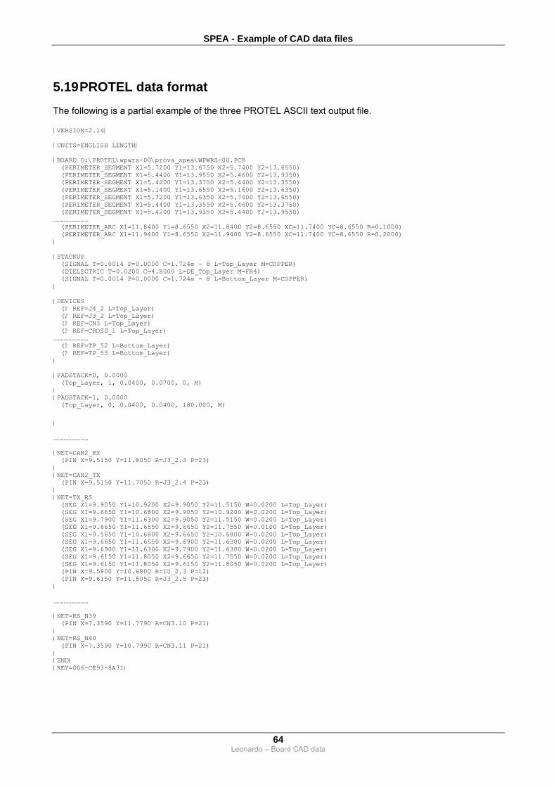
SPEA - Example of CAD data files
64 Leonardo – Board CAD data
5.19 PROTEL data format
The following is a partial example of the three PROTEL ASCII text output file. {VERSION=2.14} {UNITS=ENGLISH LENGTH} {BOARD D:\PROTEL\wpwrs-00\prova_spea\WPWRS-00.PCB (PERIMETER_SEGMENT X1=5.7200 Y1=13.6750 X2=5.7400 Y2=13.6550) (PERIMETER_SEGMENT X1=5.4400 Y1=13.9550 X2=5.4600 Y2=13.9350) (PERIMETER_SEGMENT X1=5.4200 Y1=13.3750 X2=5.4400 Y2=13.3550) (PERIMETER_SEGMENT X1=5.1400 Y1=13.6550 X2=5.1600 Y2=13.6350) (PERIMETER_SEGMENT X1=5.7200 Y1=13.6350 X2=5.7400 Y2=13.6550) (PERIMETER_SEGMENT X1=5.4400 Y1=13.3550 X2=5.4600 Y2=13.3750) (PERIMETER_SEGMENT X1=5.4200 Y1=13.9350 X2=5.4400 Y2=13.9550) ……………………… (PERIMETER_ARC X1=11.8400 Y1=8.6550 X2=11.8400 Y2=8.6550 XC=11.7400 YC=8.6550 R=0.1000) (PERIMETER_ARC X1=11.9400 Y1=8.6550 X2=11.9400 Y2=8.6550 XC=11.7400 YC=8.6550 R=0.2000) } {STACKUP (SIGNAL T=0.0014 P=0.0000 C=1.724e - 8 L=Top_Layer M=COPPER) (DIELECTRIC T=0.0200 C=4.8000 L=DE_Top_Layer M=FR4) (SIGNAL T=0.0014 P=0.0000 C=1.724e - 8 L=Bottom_Layer M=COPPER) } {DEVICES (? REF=J4_2 L=Top_Layer) (? REF=J3_2 L=Top_Layer) (? REF=CN3 L=Top_Layer) (? REF=CROSS_1 L=Top_Layer) ……………………… (? REF=TP_52 L=Bottom_Layer) (? REF=TP_53 L=Bottom_Layer) } {PADSTACK=0, 0.0000 (Top_Layer, 1, 0.0400, 0.0700, 0, M) } {PADSTACK=1, 0.0000 (Top_Layer, 0, 0.0400, 0.0400, 180.000, M)
} ……………………… {NET=CAN2_RX (PIN X=9.5150 Y=11.8050 R=J3_2.3 P=23) } {NET=CAN2_TX (PIN X=9.5150 Y=11.7050 R=J3_2.4 P=23) } {NET=TX_RS (SEG X1=9.9050 Y1=10.9200 X2=9.9050 Y2=11.5150 W=0.0200 L=Top_Layer) (SEG X1=9.6650 Y1=10.6800 X2=9.9050 Y2=10.9200 W=0.0200 L=Top_Layer) (SEG X1=9.7900 Y1=11.6300 X2=9.9050 Y2=11.5150 W=0.0200 L=Top_Layer) (SEG X1=9.6650 Y1=11.6550 X2=9.6650 Y2=11.7550 W=0.0100 L=Top_Layer) (SEG X1=9.5650 Y1=10.6800 X2=9.6650 Y2=10.6800 W=0.0200 L=Top_Layer) (SEG X1=9.6650 Y1=11.6550 X2=9.6900 Y2=11.6300 W=0.0200 L=Top_Layer) (SEG X1=9.6900 Y1=11.6300 X2=9.7900 Y2=11.6300 W=0.0200 L=Top_Layer) (SEG X1=9.6150 Y1=11.8050 X2=9.6650 Y2=11.7550 W=0.0200 L=Top_Layer) (SEG X1=9.6150 Y1=11.8050 X2=9.6150 Y2=11.8050 W=0.0200 L=Top_Layer) (PIN X=9.5800 Y=10.6800 R=IO_2.3 P=12) (PIN X=9.6150 Y=11.8050 R=J3_2.5 P=23) } ……………………… {NET=RS_N39 (PIN X=7.3590 Y=11.7790 R=CN3.10 P=21) } {NET=RS_N40 (PIN X=7.3590 Y=10.7990 R=CN3.11 P=21) } {END} {KEY=006-CE93-8A71}
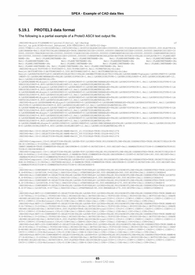
SPEA - Example of CAD data files
65 Leonardo – Board CAD data
5.19.1 PROTEL3 data format
The following is a partial example of a Protel3 ASCII text output file. |RECORD=Board|FILENAME=D:\protel3\Serial_tp\\Backup of Serial_tp.pcb|KIND=Protel_Advanced_PCB|VERSION=3.00|DATE=22-Sep-2000|TIME=11:20:23|ORIGINX=0mil|ORIGINY=0mil|BIGVISIBLEGRIDSIZE=10000000.000|VISIBLEGRIDSIZE=1000000.000|ELECTRICALGRIDRANGE=8mil|ELECTRICALGRIDENABLED=TRUE|SNAPGRIDSIZE=100000.000000|SNAPGRIDSIZEX=100000.000000|SNAPGRIDSIZEY=100000.000000|TRACKGRIDSIZE=200000.000000|VIAGRIDSIZE=200000.000000|COMPONENTGRIDSIZE=200000.000000|COMPONENTGRIDSIZEX=200000.000000|COMPONENTGRIDSIZEY=200000.000000|CURRENTWORKINGLAYER=BOTTOM|DOTGRID=FALSE|DISPLAYUNIT=1|PLANE1NETNAME=(No Net)|PLANE2NETNAME=(No Net)|PLANE3NETNAME=(No Net)|PLANE4NETNAME=(No Net)|PLANE5NETNAME=(No Net)|PLANE6NETNAME=(No Net)|PLANE7NETNAME=(No Net)|PLANE8NETNAME=(No Net)|PLANE9NETNAME=(No Net)|PLANE10NETNAME=(No Net)|PLANE11NETNAME=(No Net)|PLANE12NETNAME=(No Net)|PLANE13NETNAME=(No Net)|PLANE14NETNAME=(No Net)|PLANE15NETNAME=(No Net)|PLANE16NETNAME=(No Net) |RECORD=Board|TOPTYPE=3|TOPCONST=3.500|TOPHEIGHT=0.4mil|TOPMATERIAL=Solder Resist|BOTTOMTYPE=3|BOTTOMCONST=3.500|BOTTOMHEIGHT=0.4mil|BOTTOMMATERIAL=Solder Resist|LAYERSTACKSTYLE=0|SHOWTOPDIELECTRIC=FALSE|SHOWBOTTOMDIELECTRIC=FALSE|LAYER1NAME=TopLayer|LAYER1PREV=0|LAYER1NEXT=32|LAYER1MECHENABLED=FALSE|LAYER1COPTHICK=1.4mil|LAYER1DIELTYPE=1|LAYER1DIELCONST=4.800|LAYER1DIELHEIGHT=12.6mil|LAYER1DIELMATERIAL=FR-4|LAYER2NAME=MidLayer1|LAYER2PREV=0|LAYER2NEXT=0|LAYER2MECHENABLED=FALSE|LAYER2COPTHICK=1.4mil|LAYER2DIELTYPE=0|LAYER2DIELCONST=4.800|LAYER2DIELHEIGHT=12.6mil|LAYER2DIELMATERIAL=FR-4|LAYER3NAME=MidLayer2|LAYER3PREV=0|LAYER3NEXT=0|LAYER3MECHENABLED=FALSE|LAYER3COPTHICK=1.4mil|LAYER3DIELTYPE=0|LAYER3DIELCONST=4.800|LAYER3DIELHEIGHT=12.6mil|LAYER3DIELMATERIAL=FR-4|LAYER4NAME=MidLayer3|LAYER4PREV=0|LAYER4NEXT=0|LAYER4MECHENABLED=FALSE|LAYER4COPTHICK=1.4mil|LAYER4DIELTYPE=0|LAYER4DIELCONST=4.800|LAYER4DIELHEIGHT=12.6mil|LAYER4DIELMATERIAL=FR-4|LAYER5NAME=MidLayer4|LAYER5PREV=0|LAYER5NEXT=0|LAYER5MECHENABLED=FALSE|LAYER5COPTHICK=1.4mil|LAYER5DIELTYPE=0|LAYER5DIELCONST=4.800|LAYER5DIELHEIGHT=12.6mil|LAYER5DIELMATERIAL=FR-4 |RECORD=Board|LAYER6NAME=MidLayer5|LAYER6PREV=0|LAYER6NEXT=0|LAYER6MECHENABLED=FALSE|LAYER6COPTHICK=1.4mil|LAYER6DIELTYPE=0|LAYER6DIELCONST=4.800|LAYER6DIELHEIGHT=12.6mil|LAYER6DIELMATERIAL=FR-4|LAYER7NAME=MidLayer6|LAYER7PREV=0|LAYER7NEXT=0|LAYER7MECHENABLED=FALSE|LAYER7COPTHICK=1.4mil|LAYER7DIELTYPE=0|LAYER7DIELCONST=4.800|LAYER7DIELHEIGHT=12.6mil|LAYER7DIELMATERIAL=FR-4|LAYER8NAME=MidLayer7|LAYER8PREV=0|LAYER8NEXT=0|LAYER8MECHENABLED=FALSE|LAYER8COPTHICK=1.4mil|LAYER8DIELTYPE=0|LAYER8DIELCONST=4.800|LAYER8DIELHEIGHT=12.6mil|LAYER8DIELMATERIAL=FR-4|LAYER9NAME=MidLayer8|LAYER9PREV=0|LAYER9NEXT=0|LAYER9MECHENABLED=FALSE|LAYER9COPTHICK=1.4mil|LAYER9DIELTYPE=0|LAYER9DIELCONST=4.800|LAYER9DIELHEIGHT=12.6mil|LAYER9DIELMATERIAL=FR-4|LAYER10NAME=MidLayer9|LAYER10PREV=0|LAYER10NEXT=0|LAYER10MECHENABLED=FALSE|LAYER10COPTHICK=1.4mil|LAYER10DIELTYPE=0|LAYER10DIELCONST=4.800|LAYER10DIELHEIGHT=12.6mil|LAYER10DIELMATERIAL=FR-4 |RECORD=Net|ID=0|SELECTION=FALSE|NAME=NetU1_21|VISIBLE=TRUE|COLOR=8421376 |RECORD=Net|ID=1|SELECTION=FALSE|NAME=NetU1_49|VISIBLE=TRUE|COLOR=8421376 |RECORD=Net|ID=2|SELECTION=FALSE|NAME=NetU1_55|VISIBLE=TRUE|COLOR=8421376 ... |RECORD=Component|ID=0|SELECTION=FALSE|LAYER=TOP|LOCKED=TRUE|POLYGONOUTLINE=FALSE|USERROUTED=TRUE|PRIMITIVELOCK=TRUE|X=10800mil|Y=2200mil|PATTERN=ECN-IBMXT|NAMEON=TRUE|COMMENTON=FALSE|GROUPNUM=0|COUNT=0|ROTATION=0.000|HEIGHT=0mil|NAMEAUTOPOSITION=0|COMMENTAUTOPOSITION=0|UNIONINDEX=0 |RECORD=Component|ID=1|SELECTION=FALSE|LAYER=TOP|LOCKED=FALSE|POLYGONOUTLINE=FALSE|USERROUTED=TRUE|PRIMITIVELOCK=TRUE|X=9480mil|Y=6100mil|PATTERN=RAD0.2|NAMEON=TRUE|COMMENTON=FALSE|GROUPNUM=0|COUNT=0|ROTATION=180.000|HEIGHT=0mil|NAMEAUTOPOSITION=0|COMMENTAUTOPOSITION=0|UNIONINDEX=0 |RECORD=Component|ID=2|SELECTION=FALSE|LAYER=TOP|LOCKED=FALSE|POLYGONOUTLINE=FALSE|USERROUTED=TRUE|PRIMITIVELOCK=TRUE|X=9980mil|Y=3820mil|PATTERN=AXIAL0.4|NAMEON=TRUE|COMMENTON=TRUE|GROUPNUM=0|COUNT=0|ROTATION=180.000|HEIGHT=0mil|NAMEAUTOPOSITION=0|COMMENTAUTOPOSITION=0|UNIONINDEX=0 ... |RECORD=Arc|COMPONENT=6|SELECTION=FALSE|LAYER=TOPOVERLAY|LOCKED=FALSE|POLYGONOUTLINE=FALSE|USERROUTED=TRUE|LOCATION.X=8900mil|LOCATION.Y=4220mil|RADIUS=100mil|STARTANGLE=180.000|ENDANGLE=360.000|WIDTH=10mil|SUBPOLYINDEX=0 |RECORD=Arc|COMPONENT=6|SELECTION=FALSE|LAYER=TOPOVERLAY|LOCKED=FALSE|POLYGONOUTLINE=FALSE|USERROUTED=TRUE|LOCATION.X=8900mil|LOCATION.Y=4420mil|RADIUS=100mil|STARTANGLE=0.000|ENDANGLE=180.000|WIDTH=10mil|SUBPOLYINDEX=0 |RECORD=Arc|COMPONENT=8|SELECTION=FALSE|LAYER=TOPOVERLAY|LOCKED=FALSE|POLYGONOUTLINE=FALSE|USERROUTED=TRUE|LOCATION.X=10830mil|LOCATION.Y=4270mil|RADIUS=25mil|STARTANGLE=90.000|ENDANGLE=270.000|WIDTH=10mil|SUBPOLYINDEX=0 |RECORD=Arc|COMPONENT=9|SELECTION=FALSE|LAYER=TOPOVERLAY|LOCKED=FALSE|POLYGONOUTLINE=FALSE|USERROUTED=TRUE|LOCATION.X=9730mil|LOCATION.Y=4770mil|RADIUS=25mil|STARTANGLE=90.000|ENDANGLE=270.000|WIDTH=10mil|SUBPOLYINDEX=0 ... |RECORD=Pad|NET=12|COMPONENT=0|SELECTION=FALSE|LAYER=TOP|LOCKED=FALSE|POLYGONOUTLINE=FALSE|USERROUTED=TRUE|NAME=A31|X=7800mil|Y=2200mil|TOPXSIZE=50mil|MIDXSIZE=0mil|BOTXSIZE=0mil|TOPYSIZE=300mil|MIDYSIZE=0mil|BOTYSIZE=0mil|SHAPE=ROUND|HOLESIZE=0mil|ROTATION=0.000|PLATED=TRUE|DAISYCHAIN=Load|CCSV=1|CPLV=1|CCWV=1|CENV=1|CAGV=1|CPEV=1|CSEV=1|CPCV=1|CPRV=1|CCS=NoConnect|CPL=0|CCW=10mil|CEN=4|CAG=10mil|CPE=-150mil|CSE=4mil|CPC=20mil|CPR=20mil |RECORD=Pad|NET=13|COMPONENT=0|SELECTION=FALSE|LAYER=TOP|LOCKED=FALSE|POLYGONOUTLINE=FALSE|USERROUTED=TRUE|NAME=A30|X=7900mil|Y=2200mil|TOPXSIZE=50mil|MIDXSIZE=0mil|BOTXSIZE=0mil|TOPYSIZE=300mil|MIDYSIZE=0mil|BOTYSIZE=0mil|SHAPE=ROUND|HOLESIZE=0mil|ROTATION=0.000|PLATED=TRUE|DAISYCHAIN=Load|CCSV=1|CPLV=1|CCWV=1|CENV=1|CAGV=1|CPEV=1|CSEV=1|CPCV=1|CPRV=1|CCS=NoConnect|CPL=0|CCW=10mil|CEN=4|CAG=10mil|CPE=-150mil|CSE=4mil|CPC=20mil|CPR=20mil |RECORD=Pad|NET=14|COMPONENT=0|SELECTION=FALSE|LAYER=TOP|LOCKED=FALSE|POLYGONOUTLINE=FALSE|USERROUTED=TRUE|NAME=A29|X=8000mil|Y=2200mil|TOPXSIZE=50mil|MIDXSIZE=0mil|BOTXSIZE=0mil|TOPYSIZE=300mil|MIDYSIZE=0mil|BOTYSIZE=0mil|SHAPE=ROUND|HOLESIZE=0mil|ROTATION=0.000|PLATED=TRUE|DAISYCHAIN=Load|CCSV=1|CPLV=1|CCWV=1|CENV=1|CAGV=1|CPEV=1|CSEV=1|CPCV=1|CPRV=1|CCS=NoConnect|CPL=0|CCW=10mil|CEN=4|CAG=10mil|CPE=-150mil|CSE=4mil|CPC=20mil|CPR=20mil |RECORD=Pad|NET=109|COMPONENT=0|SELECTION=FALSE|LAYER=TOP|LOCKED=FALSE|POLYGONOUTLINE=FALSE|USERROUTED=TRUE|NAME=A28|X=8100mil|Y=2200mil|TOPXSIZE=50mil|MIDXSIZE=0mil|BOTXSIZE=0mil|TOPYSIZE=300mil|MIDYSIZE=0mil|BOTYSIZE=0mil|SHAPE=ROUND|HOLESIZE=0mil|ROTATION=0.000|PLATED=TRUE|DAISYCHAIN=Load|CCSV=1|CPLV=1|CCWV=1|CENV=1|CAGV=1|CPEV=1|CSEV=1|CPCV=1|CPRV=1|CCS=NoConnect|CPL=0|CCW=10mil|CEN=4|CAG=10mil|CPE=-150mil|CSE=4mil|CPC=20mil|CPR=20mil |RECORD=Pad|NET=108|COMPONENT=0|SELECTION=FALSE|LAYER=TOP|LOCKED=FALSE|POLYGONOUTLINE=FALSE|USERROUTED=TRUE|NAME=A27|X=8200mil|Y=2200mil|TOPXSIZE=50mil|MIDXSIZE=0mil|BOTXSIZE=0mil|TOPYSIZE=300mil|MIDYSIZE=0mil|BOTYSIZE=0mil|SHAPE=ROUND|HOLESIZE=0mil|ROTATION=0.000|PLATED=TRUE|DAISYCHAIN=Load|CCSV=1|CPLV=1|CCWV=1|CENV=1|CAGV=1|CPEV=1|CSEV=1|CPCV=1|CPRV=1|CCS=NoConnect|CPL=0|CCW=10mil|CEN=4|CAG=10mil|CPE=-150mil|CSE=4mil|CPC=20mil|CPR=20mil

SPEA - Example of CAD data files
66 Leonardo – Board CAD data
|RECORD=Pad|NET=107|COMPONENT=0|SELECTION=FALSE|LAYER=TOP|LOCKED=FALSE|POLYGONOUTLINE=FALSE|USERROUTED=TRUE|NAME=A26|X=8300mil|Y=2200mil|TOPXSIZE=50mil|MIDXSIZE=0mil|BOTXSIZE=0mil|TOPYSIZE=300mil|MIDYSIZE=0mil|BOTYSIZE=0mil|SHAPE=ROUND|HOLESIZE=0mil|ROTATION=0.000|PLATED=TRUE|DAISYCHAIN=Load|CCSV=1|CPLV=1|CCWV=1|CENV=1|CAGV=1|CPEV=1|CSEV=1|CPCV=1|CPRV=1|CCS=NoConnect|CPL=0|CCW=10mil|CEN=4|CAG=10mil|CPE=-150mil|CSE=4mil|CPC=20mil|CPR=20mil |RECORD=Pad|NET=106|COMPONENT=0|SELECTION=FALSE|LAYER=TOP|LOCKED=FALSE|POLYGONOUTLINE=FALSE|USERROUTED=TRUE|NAME=A25|X=8400mil|Y=2200mil|TOPXSIZE=50mil|MIDXSIZE=0mil|BOTXSIZE=0mil|TOPYSIZE=300mil|MIDYSIZE=0mil|BOTYSIZE=0mil|SHAPE=ROUND|HOLESIZE=0mil|ROTATION=0.000|PLATED=TRUE|DAISYCHAIN=Load|CCSV=1|CPLV=1|CCWV=1|CENV=1|CAGV=1|CPEV=1|CSEV=1|CPCV=1|CPRV=1|CCS=NoConnect|CPL=0|CCW=10mil|CEN=4|CAG=10mil|CPE=-150mil|CSE=4mil|CPC=20mil|CPR=20mil |RECORD=Pad|NET=105|COMPONENT=0|SELECTION=FALSE|LAYER=TOP|LOCKED=FALSE|POLYGONOUTLINE=FALSE|USERROUTED=TRUE|NAME=A24|X=8500mil|Y=2200mil|TOPXSIZE=50mil|MIDXSIZE=0mil|BOTXSIZE=0mil|TOPYSIZE=300mil|MIDYSIZE=0mil|BOTYSIZE=0mil|SHAPE=ROUND|HOLESIZE=0mil|ROTATION=0.000|PLATED=TRUE|DAISYCHAIN=Load|CCSV=1|CPLV=1|CCWV=1|CENV=1|CAGV=1|CPEV=1|CSEV=1|CPCV=1|CPRV=1|CCS=NoConnect|CPL=0|CCW=10mil|CEN=4|CAG=10mil|CPE=-150mil|CSE=4mil|CPC=20mil|CPR=20mil |RECORD=Pad|NET=104|COMPONENT=0|SELECTION=FALSE|LAYER=TOP|LOCKED=FALSE|POLYGONOUTLINE=FALSE|USERROUTED=TRUE|NAME=A23|X=8600mil|Y=2200mil|TOPXSIZE=50mil|MIDXSIZE=0mil|BOTXSIZE=0mil|TOPYSIZE=300mil|MIDYSIZE=0mil|BOTYSIZE=0mil|SHAPE=ROUND|HOLESIZE=0mil|ROTATION=0.000|PLATED=TRUE|DAISYCHAIN=Load|CCSV=1|CPLV=1|CCWV=1|CENV=1|CAGV=1|CPEV=1|CSEV=1|CPCV=1|CPRV=1|CCS=NoConnect|CPL=0|CCW=10mil|CEN=4|CAG=10mil|CPE=-150mil|CSE=4mil|CPC=20mil|CPR=20mil |RECORD=Pad|NET=103|COMPONENT=0|SELECTION=FALSE|LAYER=TOP|LOCKED=FALSE|POLYGONOUTLINE=FALSE|USERROUTED=TRUE|NAME=A22|X=8700mil|Y=2200mil|TOPXSIZE=50mil|MIDXSIZE=0mil|BOTXSIZE=0mil|TOPYSIZE=300mil|MIDYSIZE=0mil|BOTYSIZE=0mil|SHAPE=ROUND|HOLESIZE=0mil|ROTATION=0.000|PLATED=TRUE|DAISYCHAIN=Load|CCSV=1|CPLV=1|CCWV=1|CENV=1|CAGV=1|CPEV=1|CSEV=1|CPCV=1|CPRV=1|CCS=NoConnect|CPL=0|CCW=10mil|CEN=4|CAG=10mil|CPE=-150mil|CSE=4mil|CPC=20mil|CPR=20mil |RECORD=Pad|NET=102|COMPONENT=0|SELECTION=FALSE|LAYER=TOP|LOCKED=FALSE|POLYGONOUTLINE=FALSE|USERROUTED=TRUE|NAME=A21|X=8800mil|Y=2200mil|TOPXSIZE=50mil|MIDXSIZE=0mil|BOTXSIZE=0mil|TOPYSIZE=300mil|MIDYSIZE=0mil|BOTYSIZE=0mil|SHAPE=ROUND|HOLESIZE=0mil|ROTATION=0.000|PLATED=TRUE|DAISYCHAIN=Load|CCSV=1|CPLV=1|CCWV=1|CENV=1|CAGV=1|CPEV=1|CSEV=1|CPCV=1|CPRV=1|CCS=NoConnect|CPL=0|CCW=10mil|CEN=4|CAG=10mil|CPE=-150mil|CSE=4mil|CPC=20mil|CPR=20mil |RECORD=Pad|NET=23|COMPONENT=3|SELECTION=FALSE|LAYER=MULTILAYER|LOCKED=FALSE|POLYGONOUTLINE=FALSE|USERROUTED=TRUE|NAME=1|X=10520mil|Y=3840mil|XSIZE=62mil|YSIZE=62mil|SHAPE=ROUND|HOLESIZE=32mil|ROTATION=0.000|PLATED=TRUE|DAISYCHAIN=Load|CCSV=1|CPLV=1|CCWV=1|CENV=1|CAGV=1|CPEV=1|CSEV=1|CPCV=1|CPRV=1|CCS=Relief|CPL=0|CCW=10mil|CEN=4|CAG=10mil|CPE=0mil|CSE=4mil|CPC=20mil|CPR=20mil |RECORD=Pad|NET=119|COMPONENT=3|SELECTION=FALSE|LAYER=MULTILAYER|LOCKED=FALSE|POLYGONOUTLINE=FALSE|USERROUTED=TRUE|NAME=2|X=10720mil|Y=3840mil|XSIZE=62mil|YSIZE=62mil|SHAPE=ROUND|HOLESIZE=32mil|ROTATION=0.000|PLATED=TRUE|DAISYCHAIN=Load|CCSV=1|CPLV=1|CCWV=1|CENV=1|CAGV=1|CPEV=1|CSEV=1|CPCV=1|CPRV=1|CCS=Relief|CPL=0|CCW=10mil|CEN=4|CAG=10mil|CPE=0mil|CSE=4mil|CPC=20mil|CPR=20mil |RECORD=Pad|NET=92|COMPONENT=1|SELECTION=FALSE|LAYER=MULTILAYER|LOCKED=FALSE|POLYGONOUTLINE=FALSE|USERROUTED=TRUE|NAME=1|X=9480mil|Y=6100mil|XSIZE=62mil|YSIZE=62mil|SHAPE=ROUND|HOLESIZE=32mil|ROTATION=180.000|PLATED=TRUE|DAISYCHAIN=Load|CCSV=1|CPLV=1|CCWV=1|CENV=1|CAGV=1|CPEV=1|CSEV=1|CPCV=1|CPRV=1|CCS=Relief|CPL=0|CCW=10mil|CEN=4|CAG=10mil|CPE=0mil|CSE=4mil|CPC=10mil|CPR=20mil |RECORD=Pad|NET=119|COMPONENT=1|SELECTION=FALSE|LAYER=MULTILAYER|LOCKED=FALSE|POLYGONOUTLINE=FALSE|USERROUTED=TRUE|NAME=2|X=9280mil|Y=6100mil|XSIZE=62mil|YSIZE=62mil|SHAPE=ROUND|HOLESIZE=32mil|ROTATION=180.000|PLATED=TRUE|DAISYCHAIN=Load|CCSV=1|CPLV=1|CCWV=1|CENV=1|CAGV=1|CPEV=1|CSEV=1|CPCV=1|CPRV=1|CCS=Relief|CPL=0|CCW=10mil|CEN=4|CAG=10mil|CPE=0mil|CSE=4mil|CPC=10mil|CPR=20mil |RECORD=Pad|NET=25|COMPONENT=2|SELECTION=FALSE|LAYER=MULTILAYER|LOCKED=FALSE|POLYGONOUTLINE=FALSE|USERROUTED=TRUE|NAME=1|X=9980mil|Y=3820mil|XSIZE=62mil|YSIZE=62mil|SHAPE=ROUND|HOLESIZE=32mil|ROTATION=180.000|PLATED=TRUE|DAISYCHAIN=Load|CCSV=1|CPLV=1|CCWV=1|CENV=1|CAGV=1|CPEV=1|CSEV=1|CPCV=1|CPRV=1|CCS=Relief|CPL=0|CCW=10mil|CEN=4|CAG=10mil|CPE=0mil|CSE=4mil|CPC=10mil|CPR=20mil |RECORD=Pad|NET=24|COMPONENT=2|SELECTION=FALSE|LAYER=MULTILAYER|LOCKED=FALSE|POLYGONOUTLINE=FALSE|USERROUTED=TRUE|NAME=2|X=9580mil|Y=3820mil|XSIZE=62mil|YSIZE=62mil|SHAPE=ROUND|HOLESIZE=32mil|ROTATION=180.000|PLATED=TRUE|DAISYCHAIN=Load|CCSV=1|CPLV=1|CCWV=1|CENV=1|CAGV=1|CPEV=1|CSEV=1|CPCV=1|CPRV=1|CCS=Relief|CPL=0|CCW=10mil|CEN=4|CAG=10mil|CPE=0mil|CSE=4mil|CPC=10mil|CPR=20mil ... |RECORD=Via|NET=14|SELECTION=FALSE|LAYER=MULTILAYER|LOCKED=FALSE|POLYGONOUTLINE=FALSE|USERROUTED=TRUE|X=8000mil|Y=2810mil|DIAMETER=40mil|HOLESIZE=22mil|STARTLAYER=TOP|ENDLAYER=BOTTOM|CCSV=1|CPLV=1|CCWV=1|CENV=1|CAGV=1|CPEV=0|CSEV=1|CPCV=1|CPRV=1|CCS=Relief|CPL=0|CCW=10mil|CEN=4|CAG=10mil|CSE=4mil|CPC=20mil|CPR=20mil |RECORD=Via|NET=111|SELECTION=FALSE|LAYER=MULTILAYER|LOCKED=FALSE|POLYGONOUTLINE=FALSE|USERROUTED=TRUE|X=7900mil|Y=3320mil|DIAMETER=40mil|HOLESIZE=22mil|STARTLAYER=TOP|ENDLAYER=BOTTOM|CCSV=1|CPLV=1|CCWV=1|CENV=1|CAGV=1|CPEV=0|CSEV=1|CPCV=1|CPRV=1|CCS=Relief|CPL=0|CCW=10mil|CEN=4|CAG=10mil|CSE=4mil|CPC=20mil|CPR=20mil |RECORD=Via|NET=13|SELECTION=FALSE|LAYER=MULTILAYER|LOCKED=FALSE|POLYGONOUTLINE=FALSE|USERROUTED=TRUE|X=7860mil|Y=3680mil|DIAMETER=40mil|HOLESIZE=22mil|STARTLAYER=TOP|ENDLAYER=BOTTOM|CCSV=1|CPLV=1|CCWV=1|CENV=1|CAGV=1|CPEV=0|CSEV=1|CPCV=1|CPRV=1|CCS=Relief|CPL=0|CCW=10mil|CEN=4|CAG=10mil|CSE=4mil|CPC=20mil|CPR=20mil ... |RECORD=Track|NET=3|SELECTION=FALSE|LAYER=BOTTOM|LOCKED=FALSE|POLYGONOUTLINE=FALSE|USERROUTED=TRUE|X1=9520mil|Y1=3000mil|X2=9640mil|Y2=3000mil|WIDTH=10mil|SUBPOLYINDEX=0 |RECORD=Track|NET=3|SELECTION=FALSE|LAYER=BOTTOM|LOCKED=FALSE|POLYGONOUTLINE=FALSE|USERROUTED=TRUE|X1=9680mil|Y1=3040mil|X2=10500mil|Y2=3040mil|WIDTH=10mil|SUBPOLYINDEX=0 |RECORD=Track|NET=3|SELECTION=FALSE|LAYER=BOTTOM|LOCKED=FALSE|POLYGONOUTLINE=FALSE|USERROUTED=TRUE|X1=10580mil|Y1=2960mil|X2=10740mil|Y2=2960mil|WIDTH=10mil|SUBPOLYINDEX=0 |RECORD=Track|NET=3|SELECTION=FALSE|LAYER=BOTTOM|LOCKED=FALSE|POLYGONOUTLINE=FALSE|USERROUTED=TRUE|X1=10813mil|Y1=3050mil|X2=10830mil|Y2=3050mil|WIDTH=10mil|SUBPOLYINDEX=0 |RECORD=Track|NET=2|SELECTION=FALSE|LAYER=BOTTOM|LOCKED=FALSE|POLYGONOUTLINE=FALSE|USERROUTED=TRUE|X1=9580mil|Y1=2960mil|X2=9880mil|Y2=2960mil|WIDTH=10mil|SUBPOLYINDEX=0 |RECORD=Track|NET=1|SELECTION=FALSE|LAYER=BOTTOM|LOCKED=FALSE|POLYGONOUTLINE=FALSE|USERROUTED=TRUE|X1=9660mil|Y1=3260mil|X2=9880mil|Y2=3260mil|WIDTH=10mil|SUBPOLYINDEX=0 |RECORD=Track|NET=3|SELECTION=FALSE|LAYER=BOTTOM|LOCKED=FALSE|POLYGONOUTLINE=FALSE|USERROUTED=TRUE|X1=10760mil|Y1=2980mil|X2=10760mil|Y2=2997mil|WIDTH=10mil|SUBPOLYINDEX=0 |RECORD=Track|NET=0|SELECTION=FALSE|LAYER=BOTTOM|LOCKED=FALSE|POLYGONOUTLINE=FALSE|USERROUTED=TRUE|X1=9650mil|Y1=3120mil|X2=9670mil|Y2=3140mil|WIDTH=10mil|SUBPOLYINDEX=0 |RECORD=Track|NET=2|SELECTION=FALSE|LAYER=BOTTOM|LOCKED=FALSE|POLYGONOUTLINE=FALSE|USERROUTED=TRUE|X1=9880mil|Y1=2960mil|X2=9920mil|Y2=3000mil|WIDTH=10mil|SUBPOLYINDEX=0 |RECORD=Track|NET=1|SELECTION=FALSE|LAYER=BOTTOM|LOCKED=FALSE|POLYGONOUTLINE=FALSE|USERROUTED=TRUE|X1=9880mil|Y1=3260mil|X2=9920mil|Y2=3300mil|WIDTH=10mil|SUBPOLYINDEX=0 |RECORD=Track|NET=3|SELECTION=FALSE|LAYER=BOTTOM|LOCKED=FALSE|POLYGONOUTLINE=FALSE|USERROUTED=TRUE|X1=10740mil|Y1=2960mil|X2=10760mil|Y2=2980mil|WIDTH=10mil|SUBPOLYINDEX=0 |RECORD=Track|NET=3|SELECTION=FALSE|LAYER=BOTTOM|LOCKED=FALSE|POLYGONOUTLINE=FALSE|USERROUTED=TRUE|X1=10760mil|Y1=2997mil|X2=10813mil|Y2=3050mil|WIDTH=10mil|SUBPOLYINDEX=0

SPEA - Example of CAD data files
67 Leonardo – Board CAD data
|RECORD=Track|NET=0|SELECTION=FALSE|LAYER=BOTTOM|LOCKED=FALSE|POLYGONOUTLINE=FALSE|USERROUTED=TRUE|X1=10520mil|Y1=3140mil|X2=10620mil|Y2=3040mil|WIDTH=10mil|SUBPOLYINDEX=0 |RECORD=Track|COMPONENT=1|SELECTION=FALSE|LAYER=TOPOVERLAY|LOCKED=FALSE|POLYGONOUTLINE=FALSE|USERROUTED=TRUE|X1=9555mil|Y1=6025mil|X2=9555mil|Y2=6175mil|WIDTH=12mil|SUBPOLYINDEX=0 |RECORD=Track|COMPONENT=1|SELECTION=FALSE|LAYER=TOPOVERLAY|LOCKED=FALSE|POLYGONOUTLINE=FALSE|USERROUTED=TRUE|X1=9205mil|Y1=6025mil|X2=9205mil|Y2=6175mil|WIDTH=12mil|SUBPOLYINDEX=0 |RECORD=Track|COMPONENT=1|SELECTION=FALSE|LAYER=TOPOVERLAY|LOCKED=FALSE|POLYGONOUTLINE=FALSE|USERROUTED=TRUE|X1=9205mil|Y1=6025mil|X2=9555mil|Y2=6025mil|WIDTH=12mil|SUBPOLYINDEX=0 |RECORD=Track|COMPONENT=1|SELECTION=FALSE|LAYER=TOPOVERLAY|LOCKED=FALSE|POLYGONOUTLINE=FALSE|USERROUTED=TRUE|X1=9205mil|Y1=6175mil|X2=9555mil|Y2=6175mil|WIDTH=12mil|SUBPOLYINDEX=0 |RECORD=Track|COMPONENT=2|SELECTION=FALSE|LAYER=TOPOVERLAY|LOCKED=FALSE|POLYGONOUTLINE=FALSE|USERROUTED=TRUE|X1=9900mil|Y1=3780mil|X2=9900mil|Y2=3860mil|WIDTH=12mil|SUBPOLYINDEX=0 |RECORD=Track|COMPONENT=2|SELECTION=FALSE|LAYER=TOPOVERLAY|LOCKED=FALSE|POLYGONOUTLINE=FALSE|USERROUTED=TRUE|X1=9660mil|Y1=3780mil|X2=9660mil|Y2=3860mil|WIDTH=12mil|SUBPOLYINDEX=0 |RECORD=Track|COMPONENT=2|SELECTION=FALSE|LAYER=TOPOVERLAY|LOCKED=FALSE|POLYGONOUTLINE=FALSE|USERROUTED=TRUE|X1=9660mil|Y1=3780mil|X2=9900mil|Y2=3780mil|WIDTH=12mil|SUBPOLYINDEX=0 |RECORD=Track|COMPONENT=2|SELECTION=FALSE|LAYER=TOPOVERLAY|LOCKED=FALSE|POLYGONOUTLINE=FALSE|USERROUTED=TRUE|X1=9660mil|Y1=3860mil|X2=9900mil|Y2=3860mil|WIDTH=12mil|SUBPOLYINDEX=0 |RECORD=Track|COMPONENT=2|SELECTION=FALSE|LAYER=TOPOVERLAY|LOCKED=FALSE|POLYGONOUTLINE=FALSE|USERROUTED=TRUE|X1=9900mil|Y1=3820mil|X2=9940mil|Y2=3820mil|WIDTH=12mil|SUBPOLYINDEX=0 |RECORD=Track|COMPONENT=2|SELECTION=FALSE|LAYER=TOPOVERLAY|LOCKED=FALSE|POLYGONOUTLINE=FALSE|USERROUTED=TRUE|X1=9620mil|Y1=3820mil|X2=9660mil|Y2=3820mil|WIDTH=12mil|SUBPOLYINDEX=0 |RECORD=Track|COMPONENT=3|SELECTION=FALSE|LAYER=TOPOVERLAY|LOCKED=FALSE|POLYGONOUTLINE=FALSE|USERROUTED=TRUE|X1=10445mil|Y1=3765mil|X2=10445mil|Y2=3915mil|WIDTH=12mil|SUBPOLYINDEX=0 |RECORD=Track|COMPONENT=3|SELECTION=FALSE|LAYER=TOPOVERLAY|LOCKED=FALSE|POLYGONOUTLINE=FALSE|USERROUTED=TRUE|X1=10795mil|Y1=3765mil|X2=10795mil|Y2=3915mil|WIDTH=12mil|SUBPOLYINDEX=0 |RECORD=Track|COMPONENT=3|SELECTION=FALSE|LAYER=TOPOVERLAY|LOCKED=FALSE|POLYGONOUTLINE=FALSE|USERROUTED=TRUE|X1=10445mil|Y1=3915mil|X2=10795mil|Y2=3915mil|WIDTH=12mil|SUBPOLYINDEX=0 |RECORD=Track|COMPONENT=3|SELECTION=FALSE|LAYER=TOPOVERLAY|LOCKED=FALSE|POLYGONOUTLINE=FALSE|USERROUTED=TRUE|X1=10445mil|Y1=3765mil|X2=10795mil|Y2=3765mil|WIDTH=12mil|SUBPOLYINDEX=0 .. |RECORD=Text|SELECTION=FALSE|LAYER=TOP|LOCKED=FALSE|POLYGONOUTLINE=FALSE|USERROUTED=TRUE|X=16690mil|Y=1130mil|HEIGHT=90mil|FONT=SANSSERIF|ROTATION=0.000|MIRROR=FALSE|TEXT=.GTL|WIDTH=9mil |RECORD=Text|SELECTION=FALSE|LAYER=BOTTOM|LOCKED=FALSE|POLYGONOUTLINE=FALSE|USERROUTED=TRUE|X=16690mil|Y=1130mil|HEIGHT=90mil|FONT=SANSSERIF|ROTATION=0.000|MIRROR=FALSE|TEXT=.GBL|WIDTH=9mil |RECORD=Text|SELECTION=FALSE|LAYER=BOTTOM|LOCKED=FALSE|POLYGONOUTLINE=FALSE|USERROUTED=TRUE|X=7835mil|Y=5065mil|HEIGHT=75mil|FONT=SANSSERIF|ROTATION=0.000|MIRROR=TRUE|TEXT=P/N 4PORTSI REV A|WIDTH=8mil |RECORD=Text|COMPONENT=0|SELECTION=FALSE|LAYER=TOPOVERLAY|LOCKED=FALSE|POLYGONOUTLINE=FALSE|USERROUTED=TRUE|X=9325mil|Y=2192.4mil|HEIGHT=48mil|FONT=SANSSERIF|ROTATION=0.000|MIRROR=FALSE|TEXT=CON AT62B|WIDTH=7.2mil|COMMENT=True |RECORD=Text|COMPONENT=0|SELECTION=FALSE|LAYER=TOPOVERLAY|LOCKED=FALSE|POLYGONOUTLINE=FALSE|USERROUTED=TRUE|X=7920mil|Y=2400mil|HEIGHT=48mil|FONT=SANSSERIF|ROTATION=0.000|MIRROR=FALSE|TEXT=P1|WIDTH=7.2mil|DESIGNATOR=True |RECORD=Text|COMPONENT=1|SELECTION=FALSE|LAYER=TOPOVERLAY|LOCKED=FALSE|POLYGONOUTLINE=FALSE|USERROUTED=TRUE|X=9561mil|Y=5999mil|HEIGHT=60mil|FONT=DEFAULT|ROTATION=180.000|MIRROR=FALSE|TEXT=0.1uF|WIDTH=6mil|COMMENT=True |RECORD=Text|COMPONENT=1|SELECTION=FALSE|LAYER=TOPOVERLAY|LOCKED=FALSE|POLYGONOUTLINE=FALSE|USERROUTED=TRUE|X=9060mil|Y=6080mil|HEIGHT=60mil|FONT=DEFAULT|ROTATION=360.000|MIRROR=FALSE|TEXT=C9|WIDTH=6mil|DESIGNATOR=True |RECORD=Text|COMPONENT=2|SELECTION=FALSE|LAYER=TOPOVERLAY|LOCKED=FALSE|POLYGONOUTLINE=FALSE|USERROUTED=TRUE|X=9700mil|Y=3780mil|HEIGHT=60mil|FONT=DEFAULT|ROTATION=360.000|MIRROR=FALSE|TEXT=1K5|WIDTH=6mil|COMMENT=True |RECORD=Text|COMPONENT=2|SELECTION=FALSE|LAYER=TOPOVERLAY|LOCKED=FALSE|POLYGONOUTLINE=FALSE|USERROUTED=TRUE|X=9420mil|Y=3800mil|HEIGHT=60mil|FONT=DEFAULT|ROTATION=360.000|MIRROR=FALSE|TEXT=R2|WIDTH=6mil|DESIGNATOR=True |RECORD=Text|COMPONENT=3|SELECTION=FALSE|LAYER=TOPOVERLAY|LOCKED=FALSE|POLYGONOUTLINE=FALSE|USERROUTED=TRUE|X=10820mil|Y=3780mil|HEIGHT=60mil|FONT=DEFAULT|ROTATION=0.000|MIRROR=FALSE|TEXT=20pF|WIDTH=6mil|COMMENT=True |RECORD=Text|COMPONENT=3|SELECTION=FALSE|LAYER=TOPOVERLAY|LOCKED=FALSE|POLYGONOUTLINE=FALSE|USERROUTED=TRUE|X=10820mil|Y=3860mil|HEIGHT=60mil|FONT=DEFAULT|ROTATION=0.000|MIRROR=FALSE|TEXT=C13|WIDTH=6mil|DESIGNATOR=True ... |RECORD=Fill|SELECTION=FALSE|LAYER=TOPOVERLAY|LOCKED=FALSE|POLYGONOUTLINE=FALSE|USERROUTED=TRUE|X1=7050mil|Y1=5945mil|X2=7800mil|Y2=6145mil|ROTATION=0.000 |RECORD=Fill|SELECTION=FALSE|LAYER=TOPOVERLAY|LOCKED=FALSE|POLYGONOUTLINE=FALSE|USERROUTED=TRUE|X1=7070mil|Y1=5645mil|X2=7570mil|Y2=5845mil|ROTATION=0.000 |RECORD=Fill|SELECTION=FALSE|LAYER=TOPSOLDER|LOCKED=FALSE|POLYGONOUTLINE=FALSE|USERROUTED=TRUE|X1=7675mil|Y1=2000mil|X2=10925mil|Y2=2375mil|ROTATION=0.000
...

SPEA - Example of CAD data files
68 Leonardo – Board CAD data
5.20 REDAC CADSTAR data format
The following is a partial example of a Redac Cadstar ASCII text output file. .REM 5101-2907 -01 .CSP 20 .IFL 149.IND /.CPI /R79 611.45.2944 /R112 611.45.2944 /R77 611.34.6789 /R78 611.34.6789 ...... .EOD .PCB .IMP .ASS CMD 0 MAX 16 .... LAY 1 2 3 4 5 6 7 8 9 10 11 12 13 14 15 16 PIC 1 2 3 4 5 6 7 8 WIN 05.327 02.543 288 1000 GRI 00.025 00.025 00.100 00.100 CUR 0 0 16 1 0 0 0 2 3 0 0 2 INT 15 PAD 0 - 00.000 1 00.000 0 PAD 1 - 00.040 1 00.028 0 .... PAD 60 - 00.000 1 00.000 0 PAD 60 1 00.052 0 00.000 1 00.150 00.150 0 PAD 61 - 00.000 1 00.000 0 PAD 61 16 00.052 0 00.000 1 00.150 00.150 0 PAD 62 - 00.135 1 00.036 0 PAD 63 - 00.000 1 00.000 0 VIA 0 - 00.032 1 00.020 VIA 1 - 00.040 1 00.028 .... VIA 7 - 00.100 1 00.052 LPR 0 1 16 1 0 .... TRA 0 - 00.040 TRA 1 - 00.013 TRA 2 - 00.013 .... TEX 0 00.040 00.004 TEX 1 00.060 00.008 .... OUT 0 00.000 .... TTS - 00.012 TPS - 00.012 PPS - 00.012 FGD 1000 0 CMX 0 .BOA / 01.000 01.600 01.200 01.600 01.200 01.000 02.800 01.000 02.800 01.900 03.150 01.900 03.150 02.100 03.250 02.100 0 03.250 01.770 04.850 01.770 04.850 02.100 04.950 02.100 0 04.950 01.900 05.250 01.900 05.250 01.600 06.300 01.600 06.300 02.750 09.400 02.750 09.400 05.000

SPEA - Example of CAD data files
69 Leonardo – Board CAD data
05.250 05.000 05.250 04.920 04.800 04.920 04.800 05.000 01.000 05.000 01.000 01.600 .CMP L 5007 2 01.000 01.000 01.350 01.000 .OUT .COD 0 / 00.950 01.000 00.950 00.890 01.850 00.890 01.850 01.110 00.950 01.110 00.950 01.000 .COD 1 / 01.060 01.000 01.060 00.910 01.740 00.910 01.740 01.090 01.060 01.090 01.060 01.000 / 01.000 01.000 01.060 01.000 / 01.740 01.000 01.800 01.000 / 00.990 01.000 01.020 01.000 1 00.990 01.000 1 / 01.780 01.000 01.810 01.000 1 01.780 01.000 1 .CTX .CCP .PAD 01.000 01.000 3 01.800 01.000 3 L 999 1 01.000 01.000 01.000 01.200 .OUT .COD 0 / 00.900 01.000 00.900 00.900 01.100 00.900 01.100 01.100 00.900 01.100 00.900 01.000 .CTX .CCP .PAD 01.000 01.000 62 .COM R79 0 00.000 00.000 0 L 5007 0 0 06.100 04.700 0 0 R112 2 00.143 00.035 0 L 2501 1 3 02.380 03.200 0 0 ..... B3 0 00.000 00.000 0 L 999 0 0 09.250 04.850 0 0 .CON .REM TREE 0 .REM ROUTED .COD 6 L1 2 C23 1 L1 2 T1 8 .REM TREE 1 .COD 2 V70 2 T1 9 .REM TREE 127 .COD 2 A7 8 R117 2 .ROU .REM TREE 0 .COD 6 / L1 2 C23 1 05.900 04.100 L 1 05.900 04.595 L 1 05.905 04.600 / L1 2 T1 8 05.900 04.100 L 1 05.900 04.790 L 1

SPEA - Example of CAD data files
70 Leonardo – Board CAD data
06.375 04.790 L 1 06.500 04.665 L 1 06.705 04.665 L 1 06.820 04.550 L 1 06.820 04.295 L 1 06.965 04.150 L 1 08.700 04.150 L 1 08.700 03.900 .COP / 07.400 04.350 07.400 03.810 08.300 03.810 08.300 04.000 09.290 04.000 09.290 04.600 08.500 04.600 08.500 04.800 09.100 04.800 09.100 04.900 08.200 04.900 08.200 04.450 08.150 04.450 08.150 04.300 07.950 04.300 07.950 04.500 07.850 04.500 07.850 04.300 07.650 04.300 07.650 04.350 L 16 .TEX .MAT .ERR .EOD �
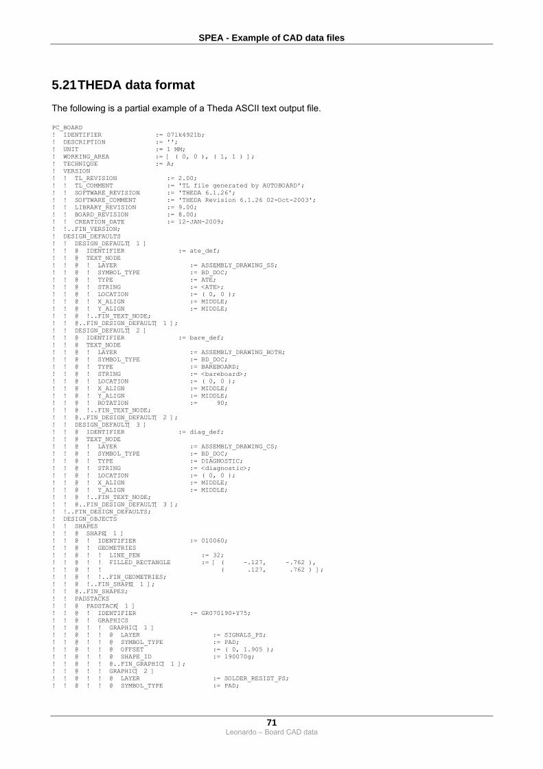
SPEA - Example of CAD data files
71 Leonardo – Board CAD data
5.21 THEDA data format
The following is a partial example of a Theda ASCII text output file. PC_BOARD ! IDENTIFIER := 07lk4921b; ! DESCRIPTION := ''; ! UNIT := 1 MM; ! WORKING_AREA := [ ( 0, 0 ), ( 1, 1 ) ]; ! TECHNIQUE := A; ! VERSION ! ! TL_REVISION := 2.00; ! ! TL_COMMENT := 'TL file generated by AUTOBOARD'; ! ! SOFTWARE_REVISION := 'THEDA 6.1.26'; ! ! SOFTWARE_COMMENT := 'THEDA Revision 6.1.26 02-Oct-2003'; ! ! LIBRARY_REVISION := 9.00; ! ! BOARD_REVISION := 8.00; ! ! CREATION_DATE := 12-JAN-2009; ! !..FIN_VERSION; ! DESIGN_DEFAULTS ! ! DESIGN_DEFAULT[ 1 ] ! ! @ IDENTIFIER := ate_def; ! ! @ TEXT_NODE ! ! @ ! LAYER := ASSEMBLY_DRAWING_SS; ! ! @ ! SYMBOL_TYPE := BD_DOC; ! ! @ ! TYPE := ATE; ! ! @ ! STRING := <ATE>; ! ! @ ! LOCATION := ( 0, 0 ); ! ! @ ! X_ALIGN := MIDDLE; ! ! @ ! Y_ALIGN := MIDDLE; ! ! @ !..FIN_TEXT_NODE; ! ! @..FIN_DESIGN_DEFAULT[ 1 ]; ! ! DESIGN_DEFAULT[ 2 ] ! ! @ IDENTIFIER := bare_def; ! ! @ TEXT_NODE ! ! @ ! LAYER := ASSEMBLY_DRAWING_BOTH; ! ! @ ! SYMBOL_TYPE := BD_DOC; ! ! @ ! TYPE := BAREBOARD; ! ! @ ! STRING := <bareboard>; ! ! @ ! LOCATION := ( 0, 0 ); ! ! @ ! X_ALIGN := MIDDLE; ! ! @ ! Y_ALIGN := MIDDLE; ! ! @ ! ROTATION := 90; ! ! @ !..FIN_TEXT_NODE; ! ! @..FIN_DESIGN_DEFAULT[ 2 ]; ! ! DESIGN_DEFAULT[ 3 ] ! ! @ IDENTIFIER := diag_def; ! ! @ TEXT_NODE ! ! @ ! LAYER := ASSEMBLY_DRAWING_CS; ! ! @ ! SYMBOL_TYPE := BD_DOC; ! ! @ ! TYPE := DIAGNOSTIC; ! ! @ ! STRING := <diagnostic>; ! ! @ ! LOCATION := ( 0, 0 ); ! ! @ ! X_ALIGN := MIDDLE; ! ! @ ! Y_ALIGN := MIDDLE; ! ! @ !..FIN_TEXT_NODE; ! ! @..FIN_DESIGN_DEFAULT[ 3 ]; ! !..FIN_DESIGN_DEFAULTS; ! DESIGN_OBJECTS ! ! SHAPES ! ! @ SHAPE[ 1 ] ! ! @ ! IDENTIFIER := 010060; ! ! @ ! GEOMETRIES ! ! @ ! ! LINE_PEN := 32; ! ! @ ! ! FILLED_RECTANGLE := [ ( -.127, -.762 ), ! ! @ ! ! ( .127, .762 ) ]; ! ! @ ! !..FIN_GEOMETRIES; ! ! @ !..FIN_SHAPE[ 1 ]; ! ! @..FIN_SHAPES; ! ! PADSTACKS ! ! @ PADSTACK[ 1 ] ! ! @ ! IDENTIFIER := GR070190+Y75; ! ! @ ! GRAPHICS ! ! @ ! ! GRAPHIC[ 1 ] ! ! @ ! ! @ LAYER := SIGNALS_PS; ! ! @ ! ! @ SYMBOL_TYPE := PAD; ! ! @ ! ! @ OFFSET := ( 0, 1.905 ); ! ! @ ! ! @ SHAPE_ID := 190070g; ! ! @ ! ! @..FIN_GRAPHIC[ 1 ]; ! ! @ ! ! GRAPHIC[ 2 ] ! ! @ ! ! @ LAYER := SOLDER_RESIST_PS; ! ! @ ! ! @ SYMBOL_TYPE := PAD;

SPEA - Example of CAD data files
72 Leonardo – Board CAD data
! ! @ ! ! @ OFFSET := ( 0, 1.905 ); ! ! @ ! ! @ SHAPE_ID := 190070g; ! ! @ ! ! @..FIN_GRAPHIC[ 2 ]; ! ! @ ! ! GRAPHIC[ 3 ] ! ! @ ! ! @ LAYER := SOLDER_PASTE_PS; ! ! @ ! ! @ SYMBOL_TYPE := PAD; ! ! @ ! ! @ OFFSET := ( 0, 1.905 ); ! ! @ ! ! @ SHAPE_ID := 190070g; ! ! @ ! ! @..FIN_GRAPHIC[ 3 ]; ! ! @ ! !..FIN_GRAPHICS; ! ! @ !..FIN_PADSTACK[ 1 ]; ! ! @..FIN_PADSTACKS; ! ! PACKAGES ! ! @ PACKAGE[ 1 ] ! ! @ ! IDENTIFIER := 0603; ! ! @ ! NUMBER_OF_PINS := 2; ! ! @ ! TYPE := '0603'; ! ! @ ! PINS ! ! @ ! ! PIN[ 1 ] ! ! @ ! ! @ NUMBER := 1; ! ! @ ! ! @ IDENTIFIER := 1; ! ! @ ! ! @ ROTATION := 90; ! ! @ ! ! @ LOCATION := ( -.6865011, 0 ); ! ! @ ! ! @ PADSTACK_ID := R032036; ! ! @ ! ! @..FIN_PIN[ 1 ]; ! ! @ ! ! PIN[ 2 ] ! ! @ ! ! @ NUMBER := 2; ! ! @ ! ! @ IDENTIFIER := 2; ! ! @ ! ! @ ROTATION := 90; ! ! @ ! ! @ LOCATION := ( .6865011, 0 ); ! ! @ ! ! @ PADSTACK_ID := R032036; ! ! @ ! ! @..FIN_PIN[ 2 ]; ! ! @ ! !..FIN_PINS; ! ! @ ! TEXT_NODES ! ! @ ! ! TEXT_NODE[ 1 ] ! ! @ ! ! @ LAYER := ASSEMBLY_DRAWING_PS; ! ! @ ! ! @ SYMBOL_TYPE := DRAWING_1; ! ! @ ! ! @ TYPE := REF_DESIGNATOR; ! ! @ ! ! @ STRING := <ref_des>; ! ! @ ! ! @ LOCATION := ( 0, 0 ); ! ! @ ! ! @ X_ALIGN := MIDDLE; ! ! @ ! ! @ Y_ALIGN := MIDDLE; ! ! @ ! ! @..FIN_TEXT_NODE[ 1 ]; ! ! @ ! ! TEXT_NODE[ 2 ] ! ! @ ! ! @ LAYER := SILK_SCREEN_PS; ! ! @ ! ! @ SYMBOL_TYPE := DRAWING_1; ! ! @ ! ! @ TYPE := REF_DESIGNATOR; ! ! @ ! ! @ STRING := <ref_des>; ! ! @ ! ! @ LOCATION := ( 0, 0 ); ! ! @ ! ! @ X_ALIGN := MIDDLE; ! ! @ ! ! @ Y_ALIGN := MIDDLE; ! ! @ ! ! @..FIN_TEXT_NODE[ 2 ]; ! ! @ ! !..FIN_TEXT_NODES; ! ! @ ! DIMENSIONS ! ! @ ! ! WEIGHT := 0; ! ! @ ! ! DIMENSION[ 1 ] ! ! @ ! ! @ LAYER := ASSEMBLY_SPACE_PS; ! ! @ ! ! @ SYMBOL_TYPE := PK_DIMENSIONS; ! ! @ ! ! @ HEIGHT := 254; ! ! @ ! ! @ LINE_PEN := 32; ! ! @ ! ! @ AREA_PEN := 2; ! ! @ ! ! @ FILLED_RECTANGLE := [ ( -1.26746, -.6324601 ), ! ! @ ! ! @ ( 1.26746, .6324601 ) ]; ! ! @ ! ! @..FIN_DIMENSION[ 1 ]; ! ! @ ! !..FIN_DIMENSIONS; ! ! @ ! DRAWINGS ! ! @ ! ! DRAWING[ 1 ] ! ! @ ! ! @ LAYER := ASSEMBLY_DRAWING_PS; ! ! @ ! ! @ SYMBOL_TYPE := DRAWING_1; ! ! @ ! ! @ LINE := [ ( -.800001, -.5999999 ), ! ! @ ! ! @ ( .800001, -.5999999 ) ]; ! ! @ ! ! @..FIN_DRAWING[ 1 ]; ! ! @ ! ! DRAWING[ 2 ] ! ! @ ! ! @ LAYER := ASSEMBLY_DRAWING_PS; ! ! @ ! ! @ SYMBOL_TYPE := DRAWING_1; ! ! @ ! ! @ LINE := [ ( .800001, .5999999 ), ! ! @ ! ! @ ( -.800001, .5999999 ) ]; ! ! @ ! ! @..FIN_DRAWING[ 2 ]; ! ! @ ! ! DRAWING[ 3 ] ! ! @ ! ! @ LAYER := ASSEMBLY_SPACE_PS; ! ! @ ! ! @ SYMBOL_TYPE := DRAWING_1; ! ! @ ! ! @ TEXT ! ! @ ! ! @ ! STRING := 1; ! ! @ ! ! @ ! LOCATION := ( -.1873538, -.5238266 );

SPEA - Example of CAD data files
73 Leonardo – Board CAD data
! ! @ ! ! @ ! X_ALIGN := NORMAL; ! ! @ ! ! @ ! Y_ALIGN := NORMAL; ! ! @ ! ! @ !..FIN_TEXT; ! ! @ ! ! @..FIN_DRAWING[ 3 ]; ! ! @ ! !..FIN_DRAWINGS; ! ! @ !..FIN_PACKAGE[ 1 ]; ! ! @..FIN_PACKAGES; ! ! DEVICES ! ! @ DEVICE[ 1 ] ! ! @ ! IDENTIFIER := 04; ! ! @ ! NUMBER_OF_PINS := 14; ! ! @ ! PIN_NAMES ! ! @ ! ! #----------------------# ! ! @ ! ! PIN_NUMBER PIN_NAME ! ! @ ! ! #----------------------# ! ! @ ! ! 1 1A ! ! @ ! ! 2 1Y ! ! @ ! ! 3 2A ! ! @ ! ! 4 2Y ! ! @ ! ! 5 3A ! ! @ ! ! 6 3Y ! ! @ ! ! 7 GND ! ! @ ! ! 8 4Y ! ! @ ! ! 9 4A ! ! @ ! ! 10 5Y ! ! @ ! ! 11 5A ! ! @ ! ! 12 6Y ! ! @ ! ! 13 6A ! ! @ ! ! 14 Vcc ! ! @ ! ! #----------------------# ! ! @ ! !..FIN_PIN_NAMES; ! ! @ ! GATE_SWAP ! ! @ ! ! GATE_SWAP_WITH_OTHERS; ! ! @ ! ! GATE_GROUP_SWAP_WITH_OTHERS; ! ! @ ! ! GROUPS ! ! @ ! ! @ GROUP[ 1 ] ! ! @ ! ! @ ! GATE[ 1 ] := [ 1, 2 ]; ! ! @ ! ! @ ! GATE[ 2 ] := [ 3, 4 ]; ! ! @ ! ! @ ! GATE[ 3 ] := [ 5, 6 ]; ! ! @ ! ! @ ! GATE[ 4 ] := [ 9, 8 ]; ! ! @ ! ! @ ! GATE[ 5 ] := [ 11, 10 ]; ! ! @ ! ! @ ! GATE[ 6 ] := [ 13, 12 ]; ! ! @ ! ! @ !..FIN_GROUP[ 1 ]; ! ! @ ! ! @..FIN_GROUPS; ! ! @ ! !..FIN_GATE_SWAP; ! ! @ ! PIN_NET_TYPES ! ! @ ! ! #--------------------------------# ! ! @ ! ! PIN_NUMBER PIN_TYPE NET_TYPE ! ! @ ! ! #--------------------------------# ! ! @ ! ! 1 INPUT LS_TTL ! ! @ ! ! 2 OUTPUT LS_TTL ! ! @ ! ! 3 INPUT LS_TTL ! ! @ ! ! 4 OUTPUT LS_TTL ! ! @ ! ! 5 INPUT LS_TTL ! ! @ ! ! 6 OUTPUT LS_TTL ! ! @ ! ! 7 BIDIR LS_TTL ! ! @ ! ! 8 OUTPUT LS_TTL ! ! @ ! ! 9 INPUT LS_TTL ! ! @ ! ! 10 OUTPUT LS_TTL ! ! @ ! ! 11 INPUT LS_TTL ! ! @ ! ! 12 OUTPUT LS_TTL ! ! @ ! ! 13 INPUT LS_TTL ! ! @ ! ! 14 BIDIR LS_TTL ! ! @ ! ! #--------------------------------# ! ! @ ! !..FIN_PIN_NET_TYPES; ! ! @ ! SERVICE_PINS ! ! @ ! ! #----------------# ! ! @ ! ! PIN_NUMBER VOLTAGE ! ! @ ! ! #----------------# ! ! @ ! ! 7 0 ! ! @ ! ! 14 5 ! ! @ ! ! #----------------# ! ! @ ! !..FIN_SERVICE_PINS; ! ! @ !..FIN_DEVICE[ 1 ]; ! ! @..FIN_DEVICES; ! ! COMPONENTS ! ! @ COMPONENT[ 1 ] ! ! @ ! IDENTIFIER := 100uf50v_v_d10p5; ! ! @ ! PACKAGE_ID := cev_10x12.5_p5; ! ! @ ! DEVICE_ID := capacita-polarizzata-2pin; ! ! @ !..FIN_COMPONENT[ 1 ]; ! ! @..FIN_COMPONENTS; ! !..FIN_DESIGN_OBJECTS; ! NET_LIST

SPEA - Example of CAD data files
74 Leonardo – Board CAD data
! ! COMPONENTS ! ! @ COMPONENT[ 1 ] ! ! @ ! REFERENCE_DESIGNATOR := C1; ! ! @ ! TYPE := NORMAL_COMPONENT; ! ! @ ! LIBRARY_IDENTIFIER := 100uf50v_v_d10p5; ! ! @ ! PIN_IDS := PHYSICAL; ! ! @ !..FIN_COMPONENT[ 1 ]; ! ! @..FIN_COMPONENTS; ! ! NETS ! ! @ NET[ 1 ] ! ! @ ! IDENTIFIER := +12V; ! ! @ ! PINS ! ! @ ! ! PIN[ 1 ] ! ! @ ! ! @ REFERENCE_DESIGNATOR := JP1; ! ! @ ! ! @ PIN_ID := 1; ! ! @ ! ! @..FIN_PIN[ 1 ]; ! ! @ ! ! PIN[ 2 ] ! ! @ ! ! @ REFERENCE_DESIGNATOR := IC5; ! ! @ ! ! @ PIN_ID := 10; ! ! @ ! ! @..FIN_PIN[ 2 ]; ! ! @ ! ! PIN[ 3 ] ! ! @ ! ! @ REFERENCE_DESIGNATOR := IC1; ! ! @ ! ! @ PIN_ID := I; ! ! @ ! ! @..FIN_PIN[ 3 ]; ! ! @ ! ! PIN[ 4 ] ! ! @ ! ! @ REFERENCE_DESIGNATOR := C1; ! ! @ ! ! @ PIN_ID := P; ! ! @ ! ! @..FIN_PIN[ 4 ]; ! ! @ ! ! PIN[ 5 ] ! ! @ ! ! @ REFERENCE_DESIGNATOR := JP2; ! ! @ ! ! @ PIN_ID := 1; ! ! @ ! ! @..FIN_PIN[ 5 ]; ! ! @ ! !..FIN_PINS; ! ! @ !..FIN_NET[ 1 ]; ! !..FIN_NET_LIST; ! PHYSICAL_LAYOUT ! ! LAYER_STRUCTURE ! ! @ #-----------------------------------------------------------# ! ! @ LAYER THICKNESS TOLERANCE DIELECTRIC NAME ! ! @ #-----------------------------------------------------------# ! ! @ COMPONENT_SIDE .2 .02 4.5 '' ! ! @ INSULATION 1.2 1.2 4.5 '' ! ! @ SOLDER_SIDE .2 .02 4.5 '' ! ! @ #-----------------------------------------------------------# ! ! @ PARTIAL_VIAS ! ! @ ! #-----------------------------# ! ! @ ! BEGIN_LAYER END_LAYER ! ! @ ! #-----------------------------# ! ! @ ! COMPONENT_SIDE SOLDER_SIDE ! ! @ ! #-----------------------------# ! ! @ !..FIN_PARTIAL_VIAS; ! ! @..FIN_LAYER_STRUCTURE; ! ! COMPONENTS ! ! @ COMPONENT[ 1 ] ! ! @ ! REFERENCE_DESIGNATOR := C1; ! ! @ ! PLACED; ! ! @ ! LAYER := COMPONENT_SIDE; ! ! @ ! ROTATION := 180; ! ! @ ! LOCATION := ( 119.0625, 89.535 ); ! ! @ ! PACKAGE ! ! @ ! ! PINS ! ! @ ! ! @ PIN[ 1 ] ! ! @ ! ! @ ! NUMBER := 1; ! ! @ ! ! @ ! IDENTIFIER := P; ! ! @ ! ! @ ! NEEDED := [ COMPONENT_SIDE, ! ! @ ! ! @ ! SOLDER_SIDE ]; ! ! @ ! ! @ ! CONTACTED := [ COMPONENT_SIDE, ! ! @ ! ! @ ! SOLDER_SIDE ]; ! ! @ ! ! @ ! LOCATION := ( 2.540001, 0 ); ! ! @ ! ! @ ! PADSTACK_ID := P64-1; ! ! @ ! ! @ !..FIN_PIN[ 1 ]; ! ! @ ! ! @ PIN[ 2 ] ! ! @ ! ! @ ! NUMBER := 2; ! ! @ ! ! @ ! IDENTIFIER := N; ! ! @ ! ! @ ! NEEDED := [ COMPONENT_SIDE, ! ! @ ! ! @ ! SOLDER_SIDE ]; ! ! @ ! ! @ ! CONTACTED := [ COMPONENT_SIDE, ! ! @ ! ! @ ! SOLDER_SIDE ]; ! ! @ ! ! @ ! LOCATION := ( -2.540001, 0 ); ! ! @ ! ! @ ! PADSTACK_ID := P64-1; ! ! @ ! ! @ !..FIN_PIN[ 2 ]; ! ! @ ! ! @..FIN_PINS; ! ! @ ! ! TEXT_NODES ! ! @ ! ! @ TEXT_NODE[ 1 ]

SPEA - Example of CAD data files
75 Leonardo – Board CAD data
! ! @ ! ! @ ! LAYER := ASSEMBLY_DRAWING_PS; ! ! @ ! ! @ ! SYMBOL_TYPE := DRAWING_1; ! ! @ ! ! @ ! TYPE := REF_DESIGNATOR; ! ! @ ! ! @ ! TEXT_PEN := 2; ! ! @ ! ! @ ! STRING := C1; ! ! @ ! ! @ ! LOCATION := ( 0, 0 ); ! ! @ ! ! @ ! X_ALIGN := MIDDLE; ! ! @ ! ! @ ! Y_ALIGN := MIDDLE; ! ! @ ! ! @ ! ROTATION := 180; ! ! @ ! ! @ !..FIN_TEXT_NODE[ 1 ]; ! ! @ ! ! @ TEXT_NODE[ 2 ] ! ! @ ! ! @ ! LAYER := SILK_SCREEN_PS; ! ! @ ! ! @ ! SYMBOL_TYPE := DRAWING_1; ! ! @ ! ! @ ! TYPE := REF_DESIGNATOR; ! ! @ ! ! @ ! TEXT_PEN := 2; ! ! @ ! ! @ ! STRING := C1; ! ! @ ! ! @ ! LOCATION := ( 6.798187, -.4169312 ); ! ! @ ! ! @ ! X_ALIGN := MIDDLE; ! ! @ ! ! @ ! Y_ALIGN := MIDDLE; ! ! @ ! ! @ ! ROTATION := 180; ! ! @ ! ! @ !..FIN_TEXT_NODE[ 2 ]; ! ! @ ! ! @..FIN_TEXT_NODES; ! ! @ ! !..FIN_PACKAGE; ! ! @ !..FIN_COMPONENT[ 1 ]; ! ! @..FIN_COMPONENTS; ! ! SIGNALS ! ! @ SIGNAL[ 1 ] ! ! @ ! IDENTIFIER := +12V; ! ! @ ! TRACES ! ! @ ! ! LAYER := SOLDER_SIDE; ! ! @ ! ! LINE_PEN := 5; ! ! @ ! ! POLYGON := [ ( 113.157, 86.48699 ), ! ! @ ! ! ( 110.1725, 83.5025 ), ! ! @ ! ! ( 110.1725, 79.0575 ), ! ! @ ! ! ( 113.3475, 75.8825 ) ]; ! ! @ ! ! LAYER := COMPONENT_SIDE; ! ! @ ! ! LINE_PEN := 9; ! ! @ ! ! LINE := [ ( 134.3112, 87.23895 ), ! ! @ ! ! ( 134.3112, 84.67703 ) ]; ! ! @ ! ! LAYER := COMPONENT_SIDE; ! ! @ ! ! LINE := [ ( 116.5225, 87.63 ), ! ! @ ! ! ( 114.6175, 87.63 ) ]; ! ! @ ! ! LAYER := COMPONENT_SIDE; ! ! @ ! ! LINE := [ ( 116.5225, 89.53499 ), ! ! @ ! ! ( 116.5225, 87.63 ) ]; ! ! @ ! ! LAYER := COMPONENT_SIDE; ! ! @ ! ! POLYGON := [ ( 118.4275, 87.63 ), ! ! @ ! ! ( 124.1425, 87.63 ), ! ! @ ! ! ( 126.6825, 90.16999 ), ! ! @ ! ! ( 130.175, 90.16999 ), ! ! @ ! ! ( 131.95, 88.39503 ), ! ! @ ! ! ( 133.2947, 88.39503 ) ]; ! ! @ ! ! LAYER := COMPONENT_SIDE; ! ! @ ! ! LINE := [ ( 116.5225, 87.63 ), ! ! @ ! ! ( 118.4275, 87.63 ) ]; ! ! @ ! ! LAYER := COMPONENT_SIDE; ! ! @ ! ! LINE := [ ( 116.5225, 89.53499 ), ! ! @ ! ! ( 114.6175, 87.63 ) ]; ! ! @ ! ! LAYER := COMPONENT_SIDE; ! ! @ ! ! LINE := [ ( 116.5225, 89.53499 ), ! ! @ ! ! ( 118.4275, 87.63 ) ]; ! ! @ ! !..FIN_TRACES; ! ! @ ! VIAS ! ! @ ! ! VIA[ 1 ] ! ! @ ! ! @ LAYER := COMPONENT_SIDE; ! ! @ ! ! @ LOCATION := ( 113.3475, 75.8825 ); ! ! @ ! ! @ NEEDED := [ COMPONENT_SIDE, ! ! @ ! ! @ SOLDER_SIDE ]; ! ! @ ! ! @ CONTACTED := [ COMPONENT_SIDE, ! ! @ ! ! @ SOLDER_SIDE ]; ! ! @ ! ! @ PADSTACK_ID := viadef-f0.4; ! ! @ ! ! @..FIN_VIA[ 1 ]; ! ! @ ! !..FIN_VIAS; ! ! @ !..FIN_SIGNAL[ 1 ]; ! ! @..FIN_SIGNALS; ! !..FIN_PHYSICAL_LAYOUT; ! !..FIN_PC_BOARD;

SPEA - Example of CAD data files
76 Leonardo – Board CAD data
5.22 THEDA UNIDAT data format
The following is a partial example of the THEDA UNIDAT text output files. %%%INFO UNIDAT_VERSION=2.1.2 DATE=27-JUL-2005 13:02:22 DELIMITER=| UNITS=MM JOB_NAME=1038313979_v04 NR_OF_PCBOARDS=1 TOP_LAYER=1 BOTTOM_LAYER=4 CADSOFTWARE=THEDA AUTOBOARD CADVERSION=6.2.15 20050407 %LAYERS CURRENT_THICKNESS=1.236 CURRENT_SIGNAL_LAYERS=4 CURRENT_PWR_GND_LAYERS=0 LAYER=COMPONENT_SIDE THICKNESS=.018 …………………… THICKNESS=.018 TOLERANCE=.001 DIELECTRIC=0 %ENDLAYERS %%%PANEL 1038313979_v04 %%OUTLINES %GRAFITEM N 1 FC 0,0,0,0 %POLY L (-6,-169) (372.8,-169) (372.8,6) (-6,6) (-6,-169) %ENDPOLY N 2 FC 0,0,0,0 %POLY L (-6,-169) (372.8,-169) (372.8,6) (-6,6) (-6,-169) %ENDPOLY N 3 FC 0,0,0,0 %POLY L (-6,-169) (372.8,-169) (372.8,6) (-6,6) (-6,-169) %ENDPOLY N 4 FC 0,0,0,0 %POLY L (-6,-169) (372.8,-169) (372.8,6) (-6,6) (-6,-169) %ENDPOLY %ENDGRAFITEM %%PANELSTRUCTURE %PANEL /usr/pcb/1038313978_v04/1038313978_v04|5.6|-30.65|270| /usr/pcb/1038313978_v04/1038313978_v04|50.8|-30.65|270| /usr/pcb/1038313978_v04/1038313978_v04|96|-30.65|270| /usr/pcb/1038313978_v04/1038313978_v04|141.2|-30.65|270| …………………… /usr/pcb/1038313978_v04/1038313978_v04|322|-151.25|270| %%FIDUCIALS fid1|||LP4LL||192.506|.810462|top||0.0|NONE %%COMPONENTS A11|||C_SMOPTPASS|Optopasser Bestueckung|P_SMPASSER_BESTUECK.1|||0|4|-2|-150|-2|-150|SMD|||||| A22|||C_SMOPTPASS|Optopasser Bestueckung|P_SMPASSER_BESTUECK.1|||0|1|-2|-150|-2|-150|SMD|||||| …………………… FIDUCIALS, Number of lines = 3 COMPONENTS, Number of lines = 2055 OTHER_DRILLINGS, Number of lines = 661 COMPONENT_PINS, Number of lines = 441 COMPONENT_TOEPRINTS, Number of lines = 1 COMPONENT_BONDS, Number of lines = 1 TEST_NEADLES, Number of lines = 95 PADS, Number of lines = 1604 PACKAGES, Number of lines = 1932 FOOTPRINTS, Number of lines = 1 BOND_WEBS, Number of lines = 1 TEST_POINTS, Number of lines = 95 VIAS, Number of lines = 129
SPEA - Example of CAD data files
77 Leonardo – Board CAD data
TRACKS, Number of lines = 2454 CONDUCTIONS, Number of lines = 1614 DRAWINGS, Number of lines = 358 DIELECTRICS, Number of lines = 1

SPEA - Example of CAD data files
78 Leonardo – Board CAD data
5.23 INTEGRA and TXF-OUT data format
The following is a partial example of the INTEGRA and TXF-OUT ASCII text output file. header { unit { mm } version { 5.0 } comment { "Datei erzeugt am 04.05.00 von Integra Station" } comment { "TXF Parser Version, 3.5 R 0.454.0" } terminal_grid { 1.500000 } lib_name { "c:\integra35\l&s_proj\ohneprei.se\4319738c_6689450b_76248700c.tc" } } global_data { track_parameter { track { width { 0.002117 } } …………………… track { width { 4.999567 } } } drill_parameter { drill { diameter { 0.300567 } } …………………… drill { diameter { 4.999567 } } } pad_parameter { pad { name { "TO263 5.08x6.35 (Loetstop oben)" } place_comp { poly_pad { coor { -2.540000,5.204883 } coor { -1.500717,5.200650 } …………………… } } place_solder { smd_pad { start { 0.000000,0.000000 } end { 0.000000,0.000000 } radius { 0.000000 } } } } …………………… via { name { "Via 2,54/1,30" } drill { 1.299633 } std_pad { diameter { 2.540000 } typ { 2 } } } } board_definition { min_dist { 0.300567 } same_net_pin_pin_distance { 0.300567 } …………………… project_title { "- No Name -" } project_version { "70.200" }

SPEA - Example of CAD data files
79 Leonardo – Board CAD data
modification_date { "04.05.00" } modification_time { "07:50" } date { "18.09.98" } time { "15:31" } creator { "obrechtg" } modificator { "werthr" } board_outline {
fixed { 0 } signal_width { 0.099483 } power_width { 0.599017 } border_rule { 1 } border_outline { coor { 0.000000,0.000000 } ……………………… arc_ccw { 39.755233,8.597900 } coor { 39.048267,8.597900 } coor { 39.046150,0.008467 } } distance { track { 0.499533 } smd_pin { 2.999317 } std_pin { 2.999317 } via { 2.999317 } copper_area { 0.499533 } } } min_copper_arae { 0.000000 } optimize_airlines { 1 } power_border_width { 0.300567 } } options { default_text_name { "top-WIN" } default_text_pos { 0.000000,0.000000 } default_text_layer { track { 0 } } default_text_lwidth { 0.300567 } ……………………… default_layer { track { 0 } } drawmode { 3 } cursor { 27 } grid { 0.000000 } snap { 0.000000 } shapefilter { 0 } trackfilter { 0 } viafilter { 0 } mm { grid { 0.001000 } ……………………… } mils { grid { 0.635000 } ……………………… } std_pins_cut { 1 } smd_pins_cut { 1 } reference_libraries { lib_name { "c:\integra35\l&s_lib\typ\dum_typ.lib" } lib_name { "c:\integra35\l&s_lib\typ\l&s_typ.lib" } } } symbol_editor_options { mm_mode { 1 } } package_editor_options { mm_mode { 1 } } schematic_options { grid_size { 3.000000 }

SPEA - Example of CAD data files
80 Leonardo – Board CAD data
mm_mode { 1 } } layer_parameter { layer { layer { track { 0 } } color { 14 } visible { 1 } layer { layer { info { 2 } }
color { 33 } visible { 0 } active { 0 } pad { 1 } blocking_area { 1 } typ { 2 } name { "Leitdruck (Carbon)" } } ……………………… variant_list { name { "alle Bauteile best<252>ckt" } name { "AZL51.00A1 4 668 9467 0 TIANMA DISPLAY" } name { "AZL51.10A1WH 4 668 9468 0 TIANMA DISPLAY" } name { "AZL51.20A1 4 668 9490 0 OPTREX DISPLAY" } name { "AZL51.30A1WH 4 668 9489 0 OPTREX DISPLAY" } active { "alle Bauteile best<252>ckt" } } attribute_definitions { attribute { name { "AeDat" } } ……………………… padstack { name { "TO263 Fl<228>che" } pad { name { "TO263 (Lotmaske)" } first_layer { solderpast { 1 } } last_layer { solderpast { 1 } } } ………………………… pad { name { "ru 2.00" } first_layer { track { 1 } } last_layer { track { 1 } } } } } } symbol_definitions { symbol { name { "U1" } net { "U1" } typ { connection } elements {

SPEA - Example of CAD data files
81 Leonardo – Board CAD data
line { start { 0.000000,3.760000 } end { -0.560000,1.500000 } } line { start { 0.560000,1.500000 } end { 0.000000,3.760000 } } line { start { 0.000000,3.010000 } end { 0.380000,1.500000 } } ……………………… symbol { name { "GND" } net { "GND" } typ { connection } elements { line { start { 0.000000,0.000000 } end { 0.000000,-3.000000 } }
solid { pivot { -3.000000,-3.300000 } size { 6.000000,0.300000 } rotation { 0.000000 } } } } shape { name { "TSOP032" } alternative_list { alternative { name { "TSOP032" } pivot { 4.872567,12.412133 } size { 9.749367,24.824267 } elements { arc { coor { -3.750733,-11.650133 } } ……………………… } component { din { "C9" } symbol { name { "CAPELK" } pivot { 198.000000,52.500000 } rotation { 270.000000 } mirror { 0 } id { "A" } placed { placed } elements { place_holder { typ { symbol } text { "#:Typ#" } pivot { 201.000000,45.000000 } ……………………… } net { name { "N85" } pin_list { pin { din { "TP107" } name { "1" }

SPEA - Example of CAD data files
82 Leonardo – Board CAD data
pin_class { 0 } gate_class { 1 } element_class { 0 } flooded { 0 } id { "A" } slpname { "1" } } text { pivot { 85.500000,34.500000 } size { 20.570000,2.000000 } rotation { 0.000000 } text { "PWM- Signal 1kHz" } } } } } }

SPEA - Example of CAD data files
83 Leonardo – Board CAD data
5.24 ULTIBOARD data format
The following is a partial example of the ULTIBOARD text output files. *P PCB 4 80 2988, 3192, -2922, -3288, 6, 3, 1, 8; (|+|+|+|) -2154, -2586 240 0 0 15 30 1 1 2 0 0 1 2 1 2 1 2 1 2 1 2 1 2 1 2 1 2 1 2 1 2 1 2 1 2 1 2 1 2 65535 65535 65535 65535 65535 65535 65535 65535 65535 65535 65535 65535 65535 65535 65535 65535 65535 65535 65535 65535 65535 65535 65535 65535 65535 65535 65535 65535 65535 65535 65535 65535 *TP ffffffff *TT 0, 10, 10 *TT 1, 10, 10 *TT 2, 10, 10 *TT 3, 8, 8 *TT 4, 12, 10 *TT 5, 14, 10 *TT 6, 16, 10 *TT 7, 18, 10 *TT 8, 24, 10 *TT 9, 30, 10 *TT 10, 36, 10 *TT 11, 42, 12 *TT 12, 48, 10 *TT 13, 60, 10 *TT 14, 66, 12 *TT 15, 72, 12 *TT 16, 84, 12 *TT 17, 90, 24 *TT 18, 102, 10 *TT 19, 108, 10 …………………… *V 2688 1872 1178 240 000000ff 0 0 0 0; *V 2694 642 1178 240 000000ff 0 0 0 0; *V 2724 240 1067 240 000000ff 0 0 0 0; *V 2736 1662 1141 240 000000ff 0 0 0 0; *V 2772 1782 1087 240 000000ff 0 0 0 0; *V 2814 48 1264 240 000000ff 0 0 0 0; *V 2826 -318 1262 240 000000ff 0 0 0 0; *V 2838 324 1143 240 000000ff 0 0 0 0; *V 2850 -96 1263 240 000000ff 0 0 0 0; *V 2868 162 1062 240 000000ff 0 0 0 0; *V 2880 -498 429 240 000000ff 0 0 0 0 546 1159 240 000000ff 0 0 0 0 1782 1143 240 000000ff 0 0 0 0; *V 2916 -462 409 240 000000ff 0 0 0 0; *V 2952 -534 1143 240 000000ff 0 0 0 0 324 1143 240 000000ff 0 0 0 0; *X 1080 -3090 48 48 180 0 2 LOMAR S.R.L. *X 1098 -3090 48 48 180 0 1 LOMAR S.R.L. *X 1122 -3168 48 48 180 0 1 BFL48A01 L.C. *X 1104 -3168 48 48 180 0 2 BFL48A01 L.S.

SPEA - Example of CAD data files
84 Leonardo – Board CAD data
5.25 ZUKEN CR5000 data format
The following is a partial example of the ZUKEN CR5000 ASCII text output file. (pcf (header (version 2.0) (unit DBUNIT) (timeZone "") ; (ctime 2000-08-11-18:06:36) ; (utime 2000-08-21-13:17:51) ; (cuser e1006210) ; (uuser koji) ) (technologyContainer (technology 4L_PN (numberOfConductorLayer 4) (padstackGroup default) (footprintLayer (layer PT (type CONDUCTIVE)) (layer PT_FLOW (type CONDUCTIVE)) (layer SR (type SOLDERRESIST)) (layer SR_FLOW (type SOLDERRESIST)) (layer MM (type METALMASK)) (layer HOLE (type HOLE)) (layer CM-A (type SYMBOLMARK)) (layer CompArea-A (type COMPAREA)) (layer MountData-B (type UNDEFINED)) (layer Place_KeepOut-B (type PROHIBIT)) (layer Outline (type UNDEFINED)) ) (nonConductiveLayer (layer Symbol-A) (layer Resist-A) (layer MetalMask-A) (layer HeightLimit-A) (layer CompArea-A) ) (conductiveLayer (layerNumber 1 (type POSI) (soldering REFLOW_2) (refer Symbol-A (type SYMBOLMARK) (userDefType 0) ) ) ) (subLayer (systemLayer (type BOARD_FIGURE)) (systemLayer (type PADSTACK)) (systemLayer (type LAYOUT_AREA)) (systemLayer (type COMP_GROUP)) (systemLayer (type COMP_GROUP_B)) (systemLayer (type BOARD_ASSY)) (systemLayer (type BASEPOINT)) (drawLayerOf (conductive 1)) (drawLayerOf (conductive 2)) (drawLayerOf (conductive 3)) (drawLayerOf (conductive 4)) (infoLayerOf (conductive 1)) (infoLayerOf (conductive 2)) (infoLayerOf (conductive 3)) (infoLayerOf (conductive 4)) ) (layerMapping (map A (correspondence (footLayer PT) (boardLayer (conductive 1) ) ) (correspondence (footLayer PT_FLOW) (boardLayer (conductive 4) ) ) ) ) )

SPEA - Example of CAD data files
85 Leonardo – Board CAD data
) (boardContainer (components (component (reference IC3) (gateCount 1) (pinCount 3) (part G36410038012) (stockId P41_G36410038012) (package PKG_G36410038012) (footprintSpec C) (footprint DQ800C) (reverseFootprint DQ900C) (originalReference IC3) (placed YES) (placementSide A) (locationLock NO) (angleLock NO) (placementSideLock NO) (isGenerated YES) (packageSymbol YES) (outOfBoard NO) (outOfBoardLocation (pt 2147483647 2147483647) ) (location (pt 6731000 7620000) ) (minRect (box (pt 6565840 7449500) (pt 6896160 7790500) ) ) (angle 0) (drawRefDes NO) (layout (layer (nonConductive Symbol-A) (refer (line (geometry (line (vertex (pt 50000 87500 (width 20320) ) (pt 155000 87500 (width 20320) ) (pt 155000 -87500 (width 20320) ) ) ) ) ) ) (refer (line (geometry (line (vertex (pt -50000 87500 (width 20320) ) (pt -155000 87500 (width 20320) ) (pt -155000 -87500 (width 20320) ) ) ) ) ) ) (refer (line (geometry (line (vertex (pt -40000 -87500 (width 20320) ) (pt 40000 -87500

SPEA - Example of CAD data files
86 Leonardo – Board CAD data
(width 20320) ) ) ) ) ) ) ) (layer (nonConductive Resist-A) (refer (surface (geometry (surface (outlineWidth 15000) (fillWidth 15000) (fillAngle 0.000000) (vertex (pt -32500 19500) (pt 32500 19500) (pt 32500 170500) (pt -32500 170500) ) ) ) ) ) (refer (surface (geometry (surface (outlineWidth 15000) (fillWidth 15000) (fillAngle 0.000000) (vertex (pt -127499 -170500) (pt -62499 -170500) (pt -62499 -19500) (pt -127499 -19500) ) ) ) ) ) (refer (surface (geometry (surface (outlineWidth 15000) (fillWidth 15000) (fillAngle 0.000000) (vertex (pt 62500 -170500) (pt 127500 -170500) (pt 127500 -19500) (pt 62500 -19500) ) ) ) ) ) ) (layer (nonConductive MetalMask-A) (refer (surface (geometry (surface (outlineWidth 15000) (fillWidth 15000) (fillAngle 0.000000) (vertex (pt -122500 -165500) (pt -67500 -165500) (pt -67500 -24500) (pt -122500 -24500) ) ) ) ) ) (refer (surface (geometry (surface (outlineWidth 15000)

SPEA - Example of CAD data files
87 Leonardo – Board CAD data
(fillWidth 15000) (fillAngle 0.000000) (vertex (pt 67500 -165500) (pt 122500 -165500) (pt 122500 -24500) (pt 67500 -24500) ) ) ) ) ) (refer (surface (geometry (surface (outlineWidth 15000) (fillWidth 15000) (fillAngle 0.000000) (vertex (pt -27500 24500) (pt 27500 24500) (pt 27500 165500) (pt -27500 165500) ) ) ) ) ) ) (layer (nonConductive CompArea-A) (refer (area (upperHeight 0) (lowerHeight 0) (geometry (surface (outlineWidth 0) (fillWidth 0) (fillAngle 0.000000) (vertex (pt -122500 -165500) (pt -122500 -87500) (pt -155000 -87500) (pt -155000 87500) (pt -27500 87500) (pt -27500 165500) (pt 27500 165500) (pt 27500 87500) (pt 155000 87500) (pt 155000 -87500) (pt 122500 -87500) (pt 122500 -165500) (pt 67500 -165500) (pt 67500 -87500) (pt -67500 -87500) (pt -67500 -165500) (pt -122500 -165500) ) ) ) ) ) ) (layer (nonConductive Marking-A) (refer (line (geometry (line (vertex (pt 0 63500 (width 20320) ) (pt 0 -63500 (width 20320) ) ) ) ) ) ) (refer (line (geometry

SPEA - Example of CAD data files
88 Leonardo – Board CAD data
(line (vertex (pt -63500 0 (width 20320) ) (pt 63500 0 (width 20320) ) ) ) ) ) ) ) (layer (nonConductive MountData-A) (pad hole0 (pt 6826000 7474500) ) (pad hole0 (pt 6636000 7474500) ) (pad hole0 (pt 6731000 7765500) ) ) (layer (nonConductive Symbol-A-1) (refer (line (geometry (line (vertex (pt 50000 87500 (width 20320) ) (pt 155000 87500 (width 20320) ) (pt 155000 -87500 (width 20320) ) ) ) ) ) ) (refer (line (geometry (line (vertex (pt -50000 87500 (width 20320) ) (pt -155000 87500 (width 20320) ) (pt -155000 -87500 (width 20320) ) ) ) ) ) ) (refer (line (geometry (line (vertex (pt -40000 -87500 (width 20320) ) (pt 40000 -87500 (width 20320) ) ) ) ) ) ) ) (layer (nonConductive Symbol-A-2) (refer (line

SPEA - Example of CAD data files
89 Leonardo – Board CAD data
(geometry (line (vertex (pt 50000 87500 (width 20320) ) (pt 155000 87500 (width 20320) ) (pt 155000 -87500 (width 20320) ) ) ) ) ) ) (refer (line (geometry (line (vertex (pt -50000 87500 (width 20320) ) (pt -155000 87500 (width 20320) ) (pt -155000 -87500 (width 20320) ) ) ) ) ) ) (refer (line (geometry (line (vertex (pt -40000 -87500 (width 20320) ) (pt 40000 -87500 (width 20320) ) ) ) ) ) ) ) ) (gate 1 (id $BF000003) (lockMode UNFIXED) (pin B (lockMode UNFIXED) ) (pin C (lockMode UNFIXED) ) (pin E (lockMode UNFIXED) ) ) (pin B (pt 6636000 7525000) (gate 1 (name B)) (layout (layer (systemLayer (type PADSTACK)) (padstack R55000X141000F (net $BN000001) (pt 6636000 7525000) (fromTo 1) (conductive (layerNumber 1 (status CONNECT)) ) ) ) ) ) (pin C
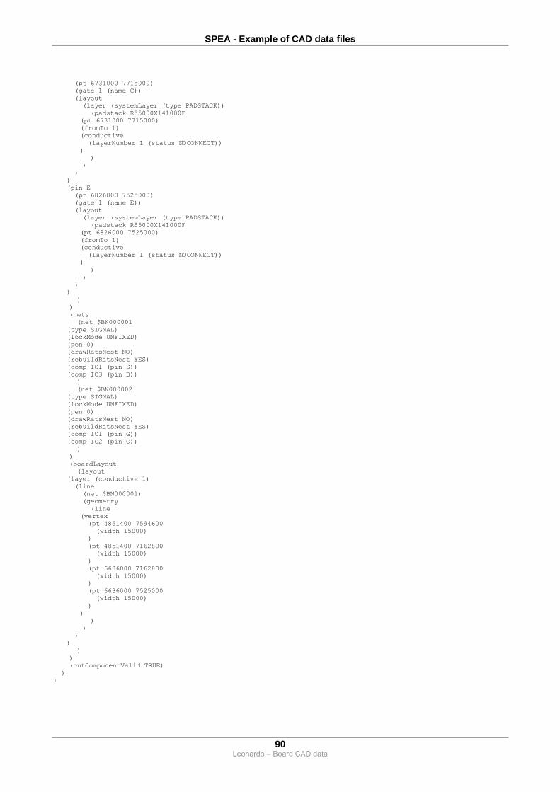
SPEA - Example of CAD data files
90 Leonardo – Board CAD data
(pt 6731000 7715000) (gate 1 (name C)) (layout (layer (systemLayer (type PADSTACK)) (padstack R55000X141000F (pt 6731000 7715000) (fromTo 1) (conductive (layerNumber 1 (status NOCONNECT)) ) ) ) ) ) (pin E (pt 6826000 7525000) (gate 1 (name E)) (layout (layer (systemLayer (type PADSTACK)) (padstack R55000X141000F (pt 6826000 7525000) (fromTo 1) (conductive (layerNumber 1 (status NOCONNECT)) ) ) ) ) ) ) ) (nets (net $BN000001 (type SIGNAL) (lockMode UNFIXED) (pen 0) (drawRatsNest NO) (rebuildRatsNest YES) (comp IC1 (pin S)) (comp IC3 (pin B)) ) (net $BN000002 (type SIGNAL) (lockMode UNFIXED) (pen 0) (drawRatsNest NO) (rebuildRatsNest YES) (comp IC1 (pin G)) (comp IC2 (pin C)) ) ) (boardLayout (layout (layer (conductive 1) (line (net $BN000001) (geometry (line (vertex (pt 4851400 7594600 (width 15000) ) (pt 4851400 7162800 (width 15000) ) (pt 6636000 7162800 (width 15000) ) (pt 6636000 7525000 (width 15000) ) ) ) ) ) ) ) ) (outComponentValid TRUE) ) )

SPEA - Example of CAD data files
91 Leonardo – Board CAD data
Version: 2 Name Date
Prepared by: A. Beltramo
Controlled by: C. Migliore, G. Dell’Aquila
Approved by: M. Raganato