leds student handout
TRANSCRIPT

7/24/2019 LEDs Student Handout
http://slidepdf.com/reader/full/leds-student-handout 1/32
Laser Diodes
Some useful characteristics of semiconductor lasers1. Capable of emitting high powers (e.g. continuous wave ~ W).
2. A relatively directional output beam (compared with LEDs) permits high coupling efficiency (~ 50 %) into single-mode fibers.
3. A relatively narrow spectral width of the emitted light allows operation at high bit rates (~ 10 Gb/s), as fiber
dispersion becomes less critical for such an optical source.
What is an LD?
• A laser diode (LD) is a semiconductor optical amplifier (SOA) that has an optical feedback.
• A semiconductor optical amplifier is a forward-biased heavily-doped p+ - n+ junction fabricated from a
direct-bandgap semiconductor material.
• The injected current is sufficiently large to provide optical gain.
• The optical feedback is usually implemented by cleaving the semiconductor material along its crystal planes.
• The sharp refractive index difference between the crystal (~3.5) and the surrounding air causes the cleaved
surfaces to act as reflectors. The semiconductor crystal therefore in general can act both as a gain medium and
as a Fabry-Perot optical resonator.

7/24/2019 LEDs Student Handout
http://slidepdf.com/reader/full/leds-student-handout 2/32
• Provided that the gain coefficient is sufficiently large, the feedback converts the optical amplifier into an
optical oscillator, i.e. a laser (Light Amplification by Stimulated Emission of R adiation)
• The device is called a laser diode or a diode laser or a semiconductor injection laser.
Fabry – Perot Interferometer.
A F.P. Interferometer consists of a highly reflective mirrors parallel to each other and whose separation is
variable.
For a single mirror, 95% of incident light is reflected and 5% is transmitted independent of wavelength.
A pair of mirrors is also highly reflective for all except certain wavelengths at which the transmission is near
100%.

7/24/2019 LEDs Student Handout
http://slidepdf.com/reader/full/leds-student-handout 3/32
For light travelling perpendicular to the mirrors, this high transmission occurs when d, the distance between the
mirrors, equals an integer number of half wavelengths i.e. when d = m (λ/2) or λ =λ m = 2d/m where m is an
integer.
The F.B. cavity is said to be RESONANT at these particular wavelengths λ m, when the waves entering or
leaving the cavity and the waves bouncing between the mirrors are all in PHASE.
Transmission for the F.P. is usually expressed in terms of the frequency. Substitution of
λ = c/v in Eq. 2.30 gives;
v = vm = )2d
cm( =
c
m
where m is an integer.
A plot of transmission of F.P. interferometer as a function of frequency consists of a series of peaks centering at
vm.
The separation between neighboring peaks 2d
c
=2d
c
m-2d
c
1)+(m=v-v= m1+m and Δσ is independent of m.
If the incident light on the interferometer has a line width Δv greater than Δσ, then the transmitted light will
have a spectrum of several lines as shown below,

7/24/2019 LEDs Student Handout
http://slidepdf.com/reader/full/leds-student-handout 4/32
If d is decreased by a factor of five or so, Δσ is then large enough so that only one peak is transmitted.
Turning semiconductor amplifiers into laser diodes.
• In the case of semiconductor lasers, external mirrors are not required as the two cleaved laser facets act as
partially reflecting mirrors.

7/24/2019 LEDs Student Handout
http://slidepdf.com/reader/full/leds-student-handout 5/32
Semiconductor as a gain medium• The basic principle: creation of population inversion, stimulated emission becomes more prevalent than
absorption.
• The population inversion is usually attained by electric-current injection in some form of a p+ - n+ junction
diode (also possible by optical pumping for basic research) => a forward bias voltage causes carrier pairs to be
injected into the junction region, where they recombine by means of stimulated emission.
• Here we discuss the semiconductor gain and bandwidth upon electrical pumping scheme.
7/24/2019 LEDs Student Handout
http://slidepdf.com/reader/full/leds-student-handout 6/32
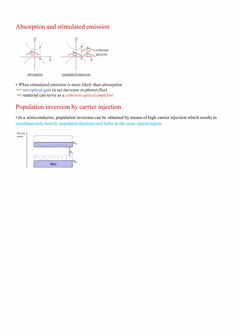
Absorption and stimulated emission
• When stimulated emission is more likely than absorption=> net optical gain (a net increase in photon flux)=> material can serve as a coherent optical amplifier .
Population inversion by carrier injection
• In a semiconductor, population inversion can be obtained by means of high carrier injection which results in
simultaneously heavily populated electrons and holes in the same spatial region.

7/24/2019 LEDs Student Handout
http://slidepdf.com/reader/full/leds-student-handout 7/32
• Incident photons with energy Eg < hv < (EFc - EFv) cannot be absorbed because the necessary conduction band
states are occupied! (and the necessary valance band states are empty)
Instead, these photons can induce downward transitions of an electron from a filled conduction band state into
an empty valence band state. => emitting coherent photons!

7/24/2019 LEDs Student Handout
http://slidepdf.com/reader/full/leds-student-handout 8/32
Population inversion in a forward-biased heavily doped p+ - n+ junction
• Upon high injection carrier density in a heavily-doped p+
- n+ junction there exist an active region near the
depletion layer, which contains simultaneously heavily populated electrons and holes – population inverted!

7/24/2019 LEDs Student Handout
http://slidepdf.com/reader/full/leds-student-handout 9/32
Population inversion in a P+- p - N
+ double heterostructure under forward bias
(e.g. AlxGa1-xAs system)
• The thin narrow-gap active region of a double heterostructure contains simultaneously heavily populatedelectrons and holes in a confined active region – population inverted!

7/24/2019 LEDs Student Handout
http://slidepdf.com/reader/full/leds-student-handout 10/32
Transition rates for semiconductors in quasi-equilibrium.
where u(v) is the spectral density, the population densities for conduction and valence bands are Pc and Pv
respectively and B12 = B21 are the Einstein coefficient for transitions.

7/24/2019 LEDs Student Handout
http://slidepdf.com/reader/full/leds-student-handout 11/32

7/24/2019 LEDs Student Handout
http://slidepdf.com/reader/full/leds-student-handout 12/32

7/24/2019 LEDs Student Handout
http://slidepdf.com/reader/full/leds-student-handout 13/32
Material transparency
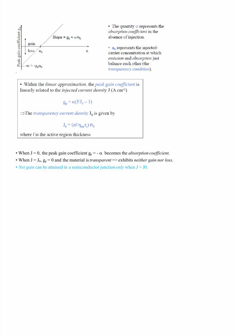
•The semiconductor material becomes “transparent” (material transparency) when the rate ofabsorption just equals the rate of stimulated emission.=> one incident photon produces exactly one photon in the output.=> the single-pass gain must be unity, i.e. G = 1.=> The material gain upon transparency g(n0) = 0.
•The transparency density n0 (number per unit volume) represents the number of excess conductionband electrons per volume required to achieve transparency.
Differential gain
•The peak gain coefficient curves can be approximated by a straight line at n0 by making a Taylorexpansion about the transparency density n0 to find
gp = gp(n)
g0(n – n0)
(n/n0 – 1)
•g0 = dgp/dn is typically called the differential gain (cm2). It has a unit of cross section.
7/24/2019 LEDs Student Handout
http://slidepdf.com/reader/full/leds-student-handout 14/32
• When J = 0, the peak gain coefficient g p = - becomes the absorption coefficient .
• When J = J0, g p = 0 and the material is transparent => exhibits neither gain nor loss.
• Net gain can be attained in a semiconductor junction only when J > J0.

7/24/2019 LEDs Student Handout
http://slidepdf.com/reader/full/leds-student-handout 15/32
Injected current density

7/24/2019 LEDs Student Handout
http://slidepdf.com/reader/full/leds-student-handout 16/32
Peak gain coefficient as a function of current density for theapproximate linear model

7/24/2019 LEDs Student Handout
http://slidepdf.com/reader/full/leds-student-handout 17/32
Example. Gain of an InGaAsP SOA
An InGaAsP semiconductor optical amplifier, operating at 300o K has the following parameters: τr = 2.5 ns, ηint
= 0.5, n0 = 1.25 x 1018 cm-3, and α = 600 cm-1. The junction has thickness l = 2 μm (not a doubleheterostructure), length d = 200 μm, and width w = 10 μm.
The transparency current density J0 = 3.2 x 10⁴ A/cm2
A slightly larger current density J = 3.5 x 10⁴ A/cm2 provides a
peak gain coefficient g p ≈ 56 cm
-1
.
An amplifier gain (i.e. single-pass gain) at the peak gain G = exp(ggd) = exp(1.12) ≈ 3However, as the junction area A = wd = 2 x 10⁻⁵ cm2, a rather large injection current i = JA = 700 mA (!) isrequired to produce this current density.
7/24/2019 LEDs Student Handout
http://slidepdf.com/reader/full/leds-student-handout 18/32
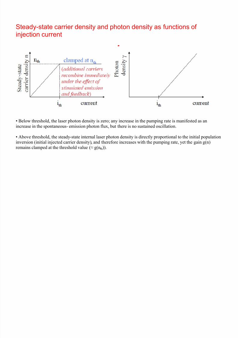
Steady-state carrier density and photon density as functions ofinjection current
• Below threshold, the laser photon density is zero; any increase in the pumping rate is manifested as an
increase in the spontaneous- emission photon flux, but there is no sustained oscillation.
• Above threshold, the steady-state internal laser photon density is directly proportional to the initial populationinversion (initial injected carrier density), and therefore increases with the pumping rate, yet the gain g(n)remains clamped at the threshold value (≈ g(nth)).

7/24/2019 LEDs Student Handout
http://slidepdf.com/reader/full/leds-student-handout 19/32
Gain at threshold
• Above threshold , the gain does not vary much from gth = g(nth).
•Recall the differential gain is the slope of the gain g(n)g0(n) = dg(n)/dn
•For lasing, the differential gain is evaluated at the threshold density nth.
•The lowest order Taylor series approximation centered on the transparency density n0 is
g(n) = g0(n – n0). => The gain at threshold must be, gth = g(nth) = g0(nth – n0)

7/24/2019 LEDs Student Handout
http://slidepdf.com/reader/full/leds-student-handout 20/32
Optical confinement factor
•The active region (i.e. gain region) has volume Va, which is smaller than the modal volume VƔ containing the optical energy.
•The simplest model assumes that the optical power is uniformly distributed in VƔ and is zero outsidethe volume.
•The optical confinement factor Γ specifies the fraction of the optical mode that overlaps the gainregion Γ = Va/ VƔ

7/24/2019 LEDs Student Handout
http://slidepdf.com/reader/full/leds-student-handout 21/32
Threshold current density

7/24/2019 LEDs Student Handout
http://slidepdf.com/reader/full/leds-student-handout 22/32
Remarks on threshold current density
• The threshold current density Jth is a key parameter in characterizing the laser-diode performance: smallervalues of J th indicate superior performance.
• Jth can be minimized by (Jth → J0 and minimizing J0):
maximizing the internal quantum efficiency ηint ;
minimizing the resonator loss coefficient αr ,
minimizing the transparency injected-carrier concentration n0,
minimizing the active-region thickness l (key merit of using double heterostructures)

7/24/2019 LEDs Student Handout
http://slidepdf.com/reader/full/leds-student-handout 23/32
Example. Threshold current for an InGaAsP heterostructure laserdiode
Consider an InGaAsP (active layer) / InP (cladding) double
heterostructure laser diode with the material parameters:
n0 = 1.25 x 1018 cm-3, α = 600 cm-1, τr = 2.5 ns, n = 3.5, ηint = 0.5
at T = 300o K. Assume that the dimensions of the junction are
d = 200 μm, w = 10 μm, and l = 0.1 μm. Assume the resonator losscoefficient αr = 118 cm-1. (assume Γ = 1)
=>The transparency current density J0 = 1600 A/cm2
=>The threshold current density Jth = 1915 A/cm2
=> The threshold current ith = 38 mA. (* Note that it is this reasonably
small threshold current that enables continuous-wave (CW) operationof double-heterostructure laser diodes at room temperature.)

7/24/2019 LEDs Student Handout
http://slidepdf.com/reader/full/leds-student-handout 24/32
7/24/2019 LEDs Student Handout
http://slidepdf.com/reader/full/leds-student-handout 25/32

7/24/2019 LEDs Student Handout
http://slidepdf.com/reader/full/leds-student-handout 26/32
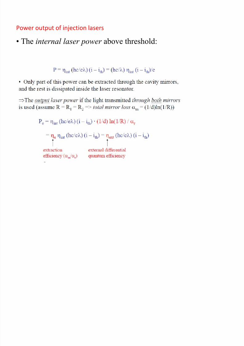
External differential quantum efficiency

7/24/2019 LEDs Student Handout
http://slidepdf.com/reader/full/leds-student-handout 27/32
Example. Efficiencies for double-heterostructure InGaAsP laser diodes

7/24/2019 LEDs Student Handout
http://slidepdf.com/reader/full/leds-student-handout 28/32
Comparison of LED and LD efficiencies and powers
When operated below threshold, laser diodes produce spontaneous emission and behave as light-emittingdiodes.
• There is a one-to-one correspondence between the efficiencies quantities for the LED and the LD.
• The superior performance of the laser results from the fact that the extraction efficiency ηe for the LD is
greater than that for the LED.
• This stems from the fact that the laser operates on the basis of stimulated emission, which causes the laser
light to be concentrated in particular modes so that it can be more readily extracted.
=> laser diode operated above threshold has a value of ηext (10’s of %)that is larger than the value of ηext for
an LED (fraction of %).

7/24/2019 LEDs Student Handout
http://slidepdf.com/reader/full/leds-student-handout 29/32

7/24/2019 LEDs Student Handout
http://slidepdf.com/reader/full/leds-student-handout 30/32

7/24/2019 LEDs Student Handout
http://slidepdf.com/reader/full/leds-student-handout 31/32
Laser diodes temporal response
• Laser diodes respond much faster than LEDs, primarily because the rise time of an LED is determined by thenatural spontaneous-emission lifetime tsp of the material.
• The rise time of a laser diode depends upon the stimulated-emission lifetime.
• In a semiconductor, the spontaneous lifetime is the average time that free charge carriers exist in the active
layer before recombining spontaneously (from injection to recombination).
• The stimulated-emission lifetime is the average time that free charge carriers exist in the active layer before
being induced to recombine by stimulated emission.
Stimulated lifetime << spontaneous lifetime
• For a laser medium to have gain, the stimulated lifetime must be shorter than the spontaneous lifetime.
• Otherwise, spontaneous recombination would occur before stimulated emission could begin, decreasing the
population inversion and inhibiting gain and oscillation.
• The faster stimulated-emission process, which dominates recombination in a laser diode, ensures that a
laser diode responds more quickly to changes in the injected current than a LED.

7/24/2019 LEDs Student Handout
http://slidepdf.com/reader/full/leds-student-handout 32/32