lecture 8: hardware security (2/2), leakage/tamper resilience...
TRANSCRIPT
1
Information Security – Theory vs. Reality
0368-4474, Winter 2015-2016
Lecture 8:Hardware security (2/2),
Leakage/tamper resilience (1/2)
Lecturer:Eran Tromer
2
Hardware security
Invasive attacks
(continued)Including presentation material by
Sergei Skorobogatov, University of Cambridge
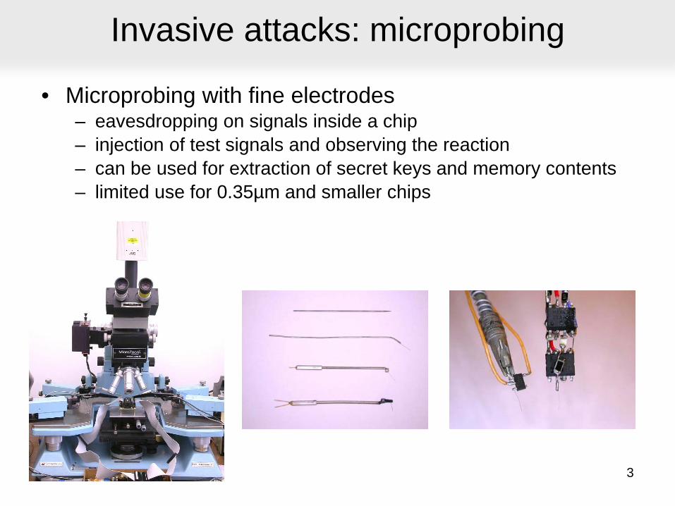
Invasive attacks: microprobing
• Microprobing with fine electrodes– eavesdropping on signals inside a chip– injection of test signals and observing the reaction– can be used for extraction of secret keys and memory contents– limited use for 0.35µm and smaller chips
3
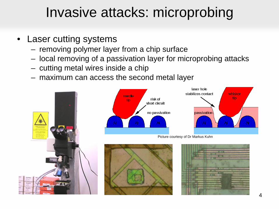
Invasive attacks: microprobing
• Laser cutting systems– removing polymer layer from a chip surface– local removing of a passivation layer for microprobing attacks– cutting metal wires inside a chip– maximum can access the second metal layer
4
Picture courtesy of Dr Markus Kuhn

Invasive attacks: chip modification
• Focused Ion Beam (FIB) workstation– chip-level surgery with 10 nm precision– etching with high aspect ratio– platinum and SiO2 deposition
5Picture courtesy of Semiresearch Ltd
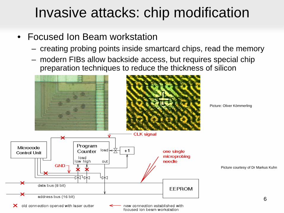
Invasive attacks: chip modification• Focused Ion Beam workstation
– creating probing points inside smartcard chips, read the memory– modern FIBs allow backside access, but requires special chip
preparation techniques to reduce the thickness of silicon
6
Picture: Oliver Kömmerling
Picture courtesy of Dr Markus Kuhn
Semi-invasive attacks
• Fill the gap between non-invasive and invasive attacks– less damaging to target device (decapsulation without penetration)– less expensive and easier to setup and repeat than invasive attacks
• Tools– IC soldering/desoldering station– simple chemical lab– high-resolution optical microscope– UV light sources, lasers– oscilloscope, logic analyser, signal generator– PC with data acquisition board, FPGA board, prototyping boards– special microscopes (laser scanning, infrared etc.)
• Types of semi-invasive attacks: passive and active– imaging: optical and laser techniques– fault injection: UV attack, photon injection, local heating, masking– side-channel attacks: optical emission analysis, induced leakage
7
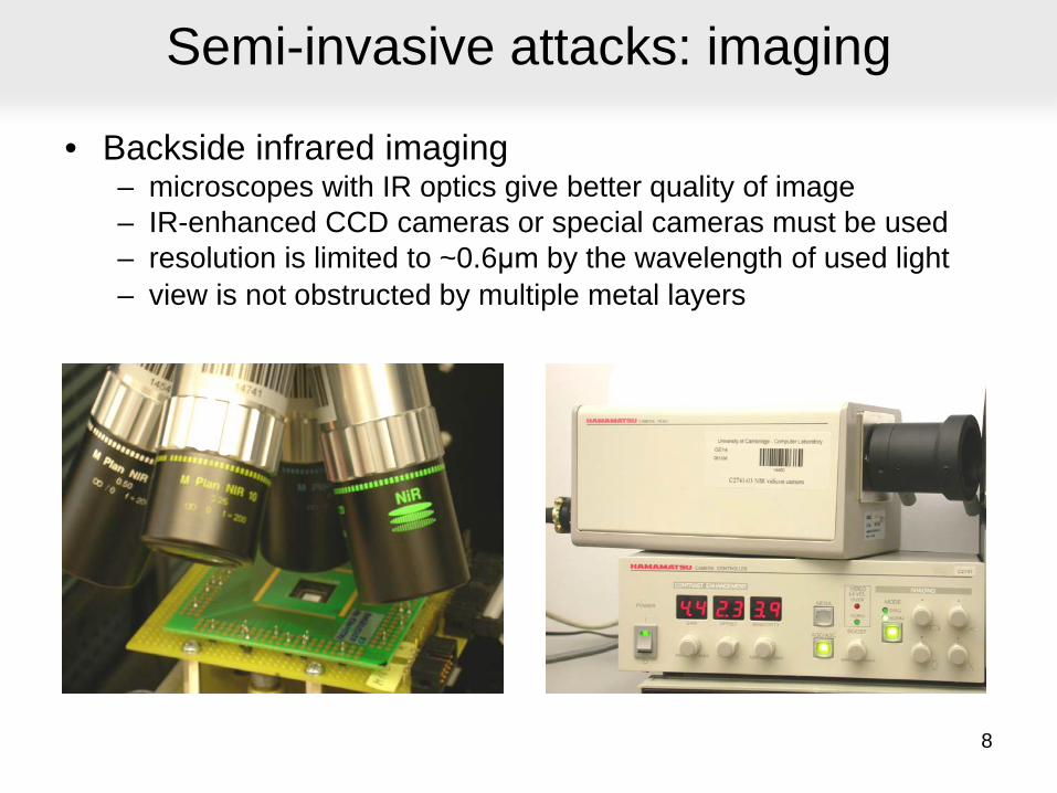
Semi-invasive attacks: imaging
• Backside infrared imaging– microscopes with IR optics give better quality of image– IR-enhanced CCD cameras or special cameras must be used– resolution is limited to ~0.6μm by the wavelength of used light– view is not obstructed by multiple metal layers
8
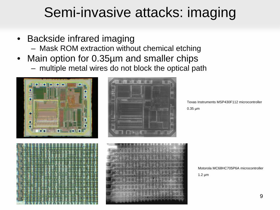
Semi-invasive attacks: imaging
• Backside infrared imaging– Mask ROM extraction without chemical etching
• Main option for 0.35µm and smaller chips– multiple metal wires do not block the optical path
9
Texas Instruments MSP430F112 microcontroller
0.35 μm
Motorola MC68HC705P6A microcontroller
1.2 μm

Semi-invasive attacks: imaging
• Advanced imaging techniques – active photon probing (Optical Beam Induced Current (OBIC))– photons with energy exceeding semiconductor band gap ionize
IC’s regions, which results in a photocurrent flow producing the image
– used for localisation of active areas– also works from the rear side of a chip (using infrared lasers)
10
Sensitivity image [mV]
100 200 300 400 500 600 700 800 900
100
200
300
400
500
600
700
800
900
0
500
1000
1500
2000
Sensitivity image [mV]
100 200 300 400 500 600 700 800 900
100
200
300
400
500
600
700
800
900 1600
1700
1800
1900
2000
2100
2200
2300
2400
2500
Microchip PIC16F84A microcontroller

Semi-invasive attacks: imaging
• Advanced imaging techniques – active photon probing (light-induced voltage alteration (LIVA) technique)– photon-induced photocurrent is dependable on the state of a
transistor– reading logic state of CMOS transistors inside a powered-up
chip– works from the rear side of a chip (using infrared lasers)
• Requires backside approach for 0.35µm and smaller chips– multiple metal wires do not block the optical path– resolution is limited to ~0.6μm (still enough for memory cells)
11
Sensitivity image [mV]
100 200 300 400 500 600 700 800 900
50
100
150
200
250
300
350
400
450
500
1000
1500
2000
2500
Sensitivity image [mV]
100 200 300 400 500 600 700 800 900
100
200
300
400
500
600
700
800
9001900
1950
2000
2050
2100
2150
Microchip PIC16F84 microcontroller

Semi-invasive attacks: fault injection
• Optical fault injection attacks– optical fault injection was observed in experiments with microprobing
attacks in early 2001, introduced as a new method in 2002– lead to new powerful attack techniques and forced chip manufacturers
to rethink their design and bring better protection– original setup involved optical microscope with a photoflash and
Microchip PIC16F84 microcontroller programmed to monitor its SRAM
12
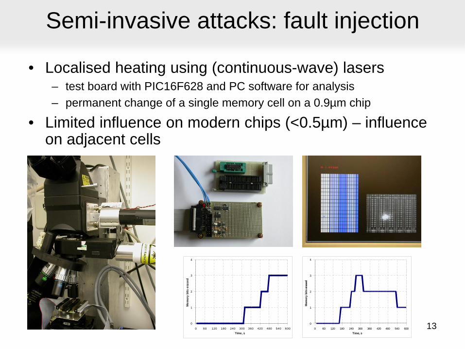
Semi-invasive attacks: fault injection
• Localised heating using (continuous-wave) lasers– test board with PIC16F628 and PC software for analysis– permanent change of a single memory cell on a 0.9µm chip
• Limited influence on modern chips (<0.5µm) – influence on adjacent cells
130 60 120 180 240 300 360 420 480 540 600
0
1
2
3
4
Time, s
Mem
ory
bits
era
sed
0 60 120 180 240 300 360 420 480 540 600
0
1
2
3
4
Time, s
Mem
ory
bits
era
sed

Semi-invasive attacks: fault injection
• Memory masking attacks– temporarily disable write and erase operations in embedded memory
(Flash/EEPROM) and write into volatile memory (SRAM)– use cw red lasers for front-side and infrared lasers for backside attacks
14
Memory Write O perationsChip Flash Cells Flash Lines Flash Array EEPROM Cell EEPROM Lines EEPROM ArrayPIC16F628A 1 – 2 1 – 2 Yes 1 – 2 1 – 2 Yes
12 – 45 1 – 2 Yes 8 – 22 1 – 2 YesPIC16F628A (backside)

Semi-invasive attacks: side-channel
• Optically enhanced position-locked power analysis– Microchip PIC16F84 microcontroller with test program at 4 MHz– classic power analysis setup (10 Ω resistor in GND, digital
storage oscilloscope) plus laser microscope scanning setup– test pattern
• run the code inside the microcontroller and store the power trace• point the laser at a particular transistor and store the power trace• compare two traces
15
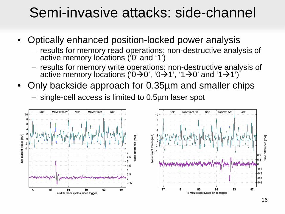
Semi-invasive attacks: side-channel
• Optically enhanced position-locked power analysis– results for memory read operations: non-destructive analysis of
active memory locations (‘0’ and ‘1’)– results for memory write operations: non-destructive analysis of
active memory locations (‘00’, ‘01’, ‘10’ and ‘11’)• Only backside approach for 0.35µm and smaller chips
– single-cell access is limited to 0.5µm laser spot
16
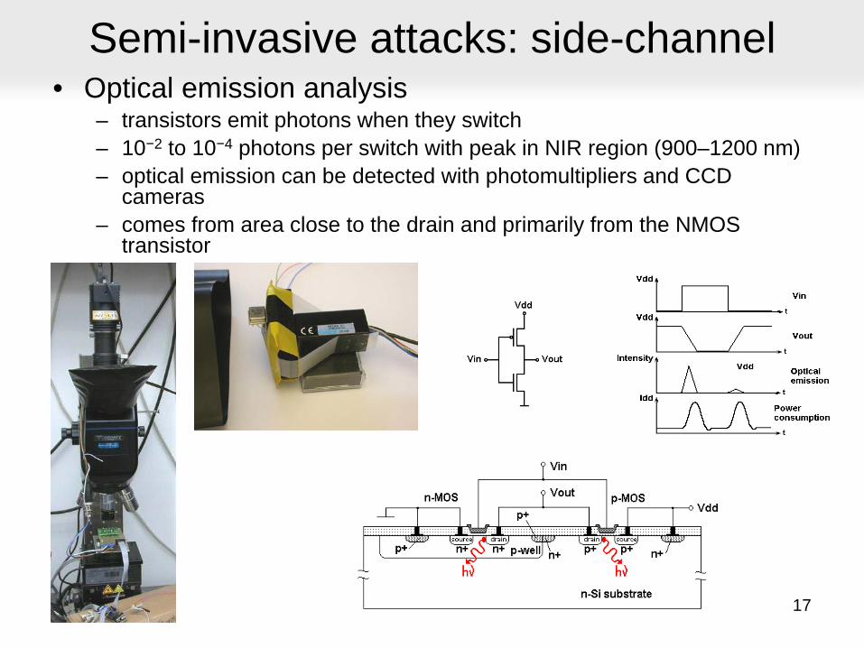
Semi-invasive attacks: side-channel• Optical emission analysis
– transistors emit photons when they switch– 10−2 to 10−4 photons per switch with peak in NIR region (900–1200 nm)– optical emission can be detected with photomultipliers and CCD
cameras– comes from area close to the drain and primarily from the NMOS
transistor
17
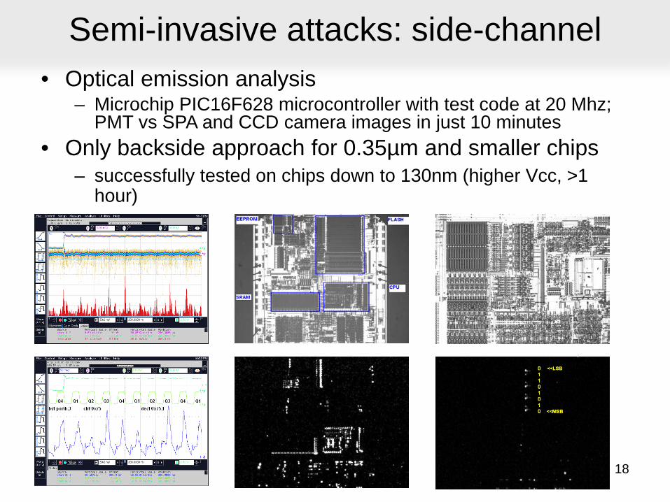
Semi-invasive attacks: side-channel• Optical emission analysis
– Microchip PIC16F628 microcontroller with test code at 20 Mhz; PMT vs SPA and CCD camera images in just 10 minutes
• Only backside approach for 0.35µm and smaller chips– successfully tested on chips down to 130nm (higher Vcc, >1
hour)
18
19
Hardware tamper protection

Tamper protection
• Old devices– security fuse is placed separately from the memory array (easy
to locate and defeat)– security fuse is embedded into the program memory (hard to
locate and defeat), similar approach is used in many smartcards in the form of password protection and encryption keys
– moving away from building blocks which are easily identifiable and have easily traceable data paths
20Motorola MC68HC908AZ60A microcontroller Scenix SX28 microcontroller

Tamper protection
• Help came from chip fabrication technology– planarisation as a part of modern chip fabrication process
(0.5 μm or smaller feature size)– glue logic design makes reverse engineering much harder– multiple metal layers block any direct access– small size of transistors makes attacks less feasible– chips operate at higher frequency and consume less power– smaller and BGA packages scare off many attackers
21
0.9µm microcontroller 0.5µm microcontroller 0.13µm FPGA

Tamper protection
• Additional protections– top metal layers with sensors– voltage, frequency and temperature sensors– memory access protection, crypto-coprocessors– internal clocks, power supply pumps– asynchronous logic design, symmetric design, dual-rail logic– ASICs, secure FPGAs and custom-designed ICs– software countermeasures
22STMicroelectronics ST16 smartcard Fujitsu secure microcontroller

Tamper protection: what goes wrong
• Security advertising without proof– no means of comparing security, lack of independent analysis– no guarantee and no responsibility from chip manufacturers– wide use of magic words: protection, encryption, authentication,
unique, highly secure, strong defence, cannot be, unbreakable, impossible, uncompromising, buried under x metal layers
• Constant economics pressure on cost reduction– less investment, hence, cheaper solutions and outsourcing– security via obscurity approach
• Quicker turnaround– less testing, hence, more bugs
• What about back-doors?– access to the on-chip data for factory testing purposes– how reliably was this feature disabled?– how difficult is to attack the access port?– are there any trojans deliberately inserted by subcontractors?
23
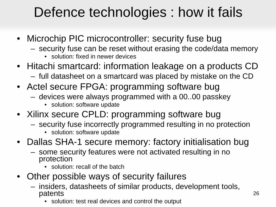
Defence technologies : how it fails
• Microchip PIC microcontroller: security fuse bug– security fuse can be reset without erasing the code/data memory
• solution: fixed in newer devices
• Hitachi smartcard: information leakage on a products CD– full datasheet on a smartcard was placed by mistake on the CD
• Actel secure FPGA: programming software bug– devices were always programmed with a 00..00 passkey
• solution: software update
• Xilinx secure CPLD: programming software bug– security fuse incorrectly programmed resulting in no protection
• solution: software update
• Dallas SHA-1 secure memory: factory initialisation bug– some security features were not activated resulting in no
protection• solution: recall of the batch
• Other possible ways of security failures– insiders, datasheets of similar products, development tools,
patents• solution: test real devices and control the output
26
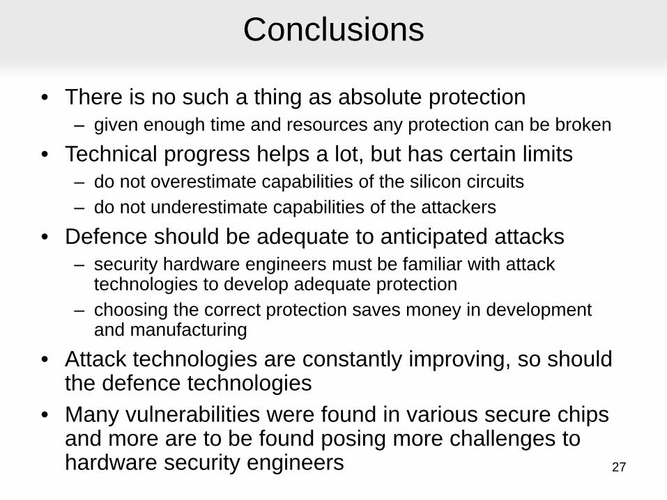
Conclusions
• There is no such a thing as absolute protection– given enough time and resources any protection can be broken
• Technical progress helps a lot, but has certain limits– do not overestimate capabilities of the silicon circuits– do not underestimate capabilities of the attackers
• Defence should be adequate to anticipated attacks– security hardware engineers must be familiar with attack
technologies to develop adequate protection– choosing the correct protection saves money in development
and manufacturing• Attack technologies are constantly improving, so should
the defence technologies• Many vulnerabilities were found in various secure chips
and more are to be found posing more challenges to hardware security engineers 27
29
Leakage and Tamper Resilience(1/2)
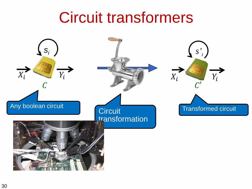
Circuit transformers
30
si
𝑋𝑋𝑖𝑖 𝑌𝑌𝑖𝑖
Any boolean circuitCircuit transformation
Transformed circuit
𝑌𝑌𝑖𝑖
'is
𝑋𝑋𝑖𝑖𝐶𝐶𝐶𝐶𝐶

Circuit transformers
• Transformer 𝑇𝑇 = (𝑇𝑇𝐶𝐶 ,𝑇𝑇𝑠𝑠)
• 𝐶𝐶𝑇𝑇𝐶𝐶 𝐶𝐶𝐶, s0 →
𝑇𝑇𝑠𝑠 𝑠𝑠0′
• 𝑇𝑇 may be randomized• 𝐶𝐶𝐶 may be randomized or (better yet) deterministic• Functionally equivalent in input-output behavior:
𝐶𝐶 𝑆𝑆0 ≈ 𝐶𝐶′[𝑠𝑠0′ ](There is a security parameter everywhere; we keep it implicit.)
31
𝑠𝑠𝑖𝑖
𝑋𝑋𝑖𝑖 𝑌𝑌𝑖𝑖 𝑌𝑌𝑖𝑖
'is
𝑋𝑋𝑖𝑖𝐶𝐶𝐶𝐶𝐶

32
𝑋𝑋𝑖𝑖 𝑌𝑌𝑖𝑖 𝑌𝑌𝑖𝑖𝑋𝑋𝑖𝑖
blackbox
indistinguishable
Security [Ishai Sahai Wagner ’03]
𝐶𝐶𝐶𝐶𝐶admissible leakage/
tampering
adversarysimulator
𝑠𝑠𝑖𝑖 𝑠𝑠𝑖𝑖′
Adversary chooses a leakage/tampering function, from a given set of admissible leakage/tampering functions, to be applied to the wires.
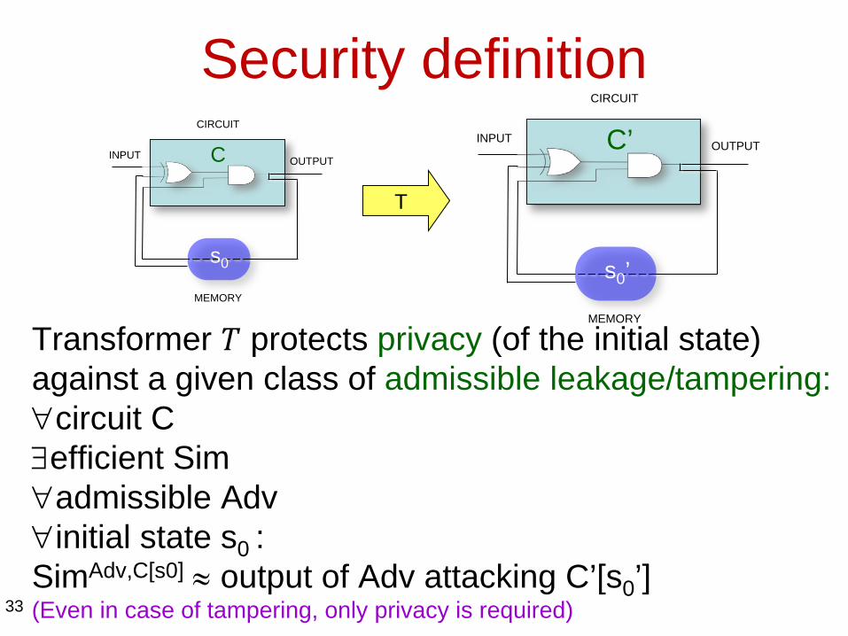
INPUT OUTPUT
CIRCUIT
MEMORY
Security definition
Transformer 𝑇𝑇 protects privacy (of the initial state)against a given class of admissible leakage/tampering:∀circuit C∃efficient Sim ∀admissible Adv∀initial state s0 :SimAdv,C[s0] ≈ output of Adv attacking C’[s0’](Even in case of tampering, only privacy is required)
CINPUT OUTPUT
CIRCUIT
MEMORY
T
C’
s0 s0’
33
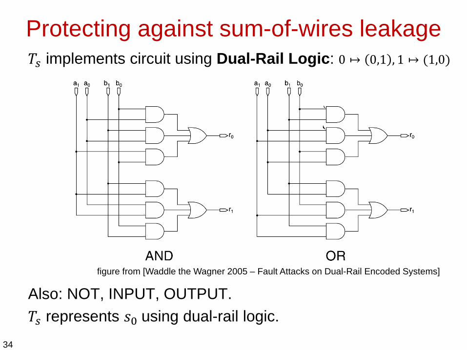
Protecting against sum-of-wires leakage𝑇𝑇𝑠𝑠 implements circuit using Dual-Rail Logic: 0 ↦ 0,1 , 1 ↦ (1,0)
34
figure from [Waddle the Wagner 2005 – Fault Attacks on Dual-Rail Encoded Systems]
Also: NOT, INPUT, OUTPUT.𝑇𝑇𝑠𝑠 represents 𝑠𝑠0 using dual-rail logic.
Protecting against sum-of-wires leakage(cont.)
• Security proof sketch: simulator runs adversary and, when asked for leakage value, answers with the constant (thus known) Hamming weight.
• Also handles weighted sum(e.g., different capacitance for long vs. short wires), as long as pairs are balanced.
• Practical complications:– Capacitance imbalance– Timing imbalance– Glitches– Cell internals
35