lecture 3 diodes - 首页hsic.sjtu.edu.cn/.../files/lec11_diodes.pdfthe rectifier converts ac...
TRANSCRIPT

Lecture 11
Diodes
1

2
Diode:
The simplest and most fundamental nonlinear circuit element.
Used as the generation of dc voltages from the ac power supply.
Foundation for understanding the characteristics of bipolar
transistors and the field-effect transistors.
Silicon pn-junction diodes .
Specialized diodes types:
photodiode
the light-emitting diode.

1. Ideal diode
3
anode Cathode
reverse biasForward bias
i
vi-v curve
diode circuit symbol
Nonlinear characteristics:
1. cutoff state: When the diode is reverse-biased , it
behaves as an open circuit.
2. On state: when the diode is forward-biased, it
behaves as an short circuit.
i-v curve includes two straight line, so it is
piecewise linear . The diode is a linear circuit in a
particular operation region.
Diode application
1. The rectifier converts ac voltage to
dc voltage.
2. Diode logic gate: such as “OR” gate
and “AND” gate.
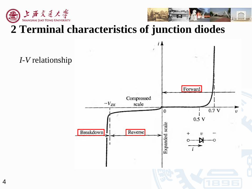
2 Terminal characteristics of junction diodes
4
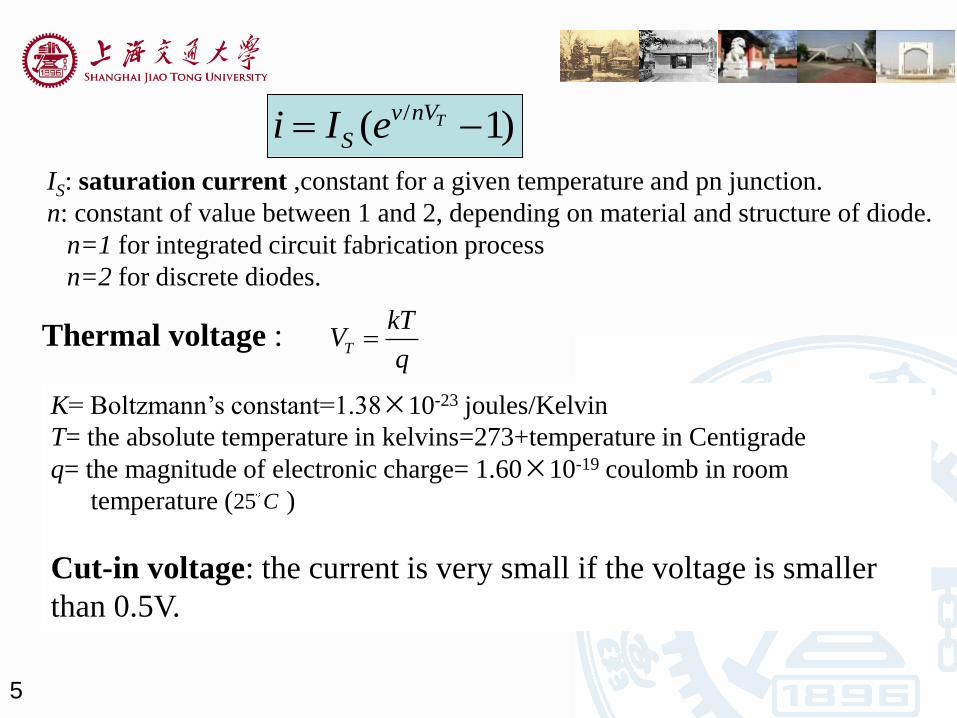
I-V relationship
5
/( 1)Tv nV
Si I e
IS: saturation current ,constant for a given temperature and pn junction.
n: constant of value between 1 and 2, depending on material and structure of diode.
n=1 for integrated circuit fabrication process
n=2 for discrete diodes.
Thermal voltage : T
kTV
q
K= Boltzmann’s constant=1.38×10⁻²³ joules/Kelvin
T= the absolute temperature in kelvins=273+temperature in Centigrade
q= the magnitude of electronic charge= 1.60×10⁻¹⁹ coulomb in room
temperature ( )
Cut-in voltage: the current is very small if the voltage is smaller
than 0.5V.
25 C

6
Physics of forward bias:
Diode Current equation:
• Junction potential φJ (potential drop across SCR)
reduced by VD ⇒minority carrier injection into QNRs
• Minority carrier diffusion through QNRs
• Minority carrier recombination at contacts to the QNRs (and
surfaces)
• Large supply of carriers injected into the QNRs
0[exp( ) 1]DD
qVI I
kT
[exp( )]DD
qVI
kT

7
Physics of reverse bias:
• Junction potential φJ (potential drop across SCR)
increased by |VD| ⇒minority carrier extraction from QNRs
• Minority carrier drift through QNRs
• Minority carrier generation at surfaces & contacts of QNRs
• Very small supply of carriers available for
Extraction ⇒ I saturates to small value
0[exp( ) 1]DD
qVI I
kT
0DI I
8
The pn junction in the
breakdown region When the reverse voltage exceeds the breakdown voltage, the
diode is breakdown. Or if the reverse current I is greater than
the drift current Is, breakdown occurs.
The two possible breakdown mechanisms :
zener effect (齐纳效应)
avalanche effect. (雪崩效应)
pn junction breakdown is not a destructive process, provided
that the maximum specified power dissipation is not exceeded.
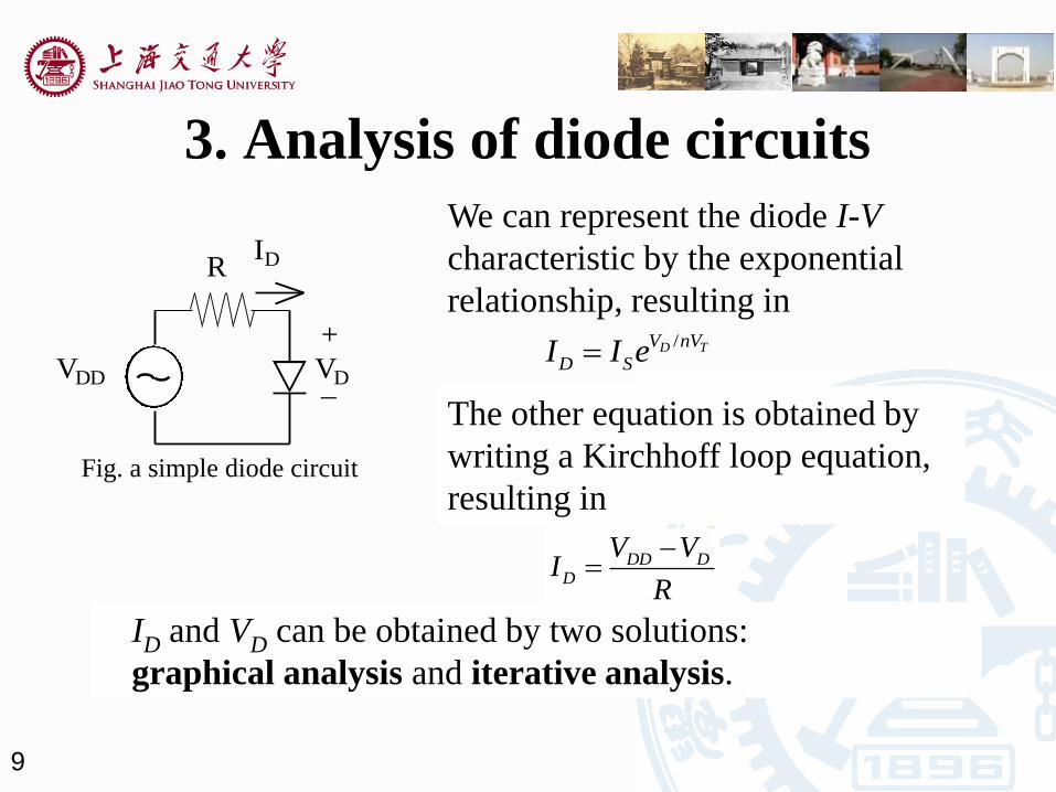
3. Analysis of diode circuits
9
VDD
R
+
VD_
ID
Fig. a simple diode circuit
We can represent the diode I-V
characteristic by the exponential
relationship, resulting in /D TV nV
D SI I e
The other equation is obtained by
writing a Kirchhoff loop equation,
resulting in
DD DD
V VI
R
ID and VD can be obtained by two solutions:
graphical analysis and iterative analysis.

Graphical analysis
10
The operation point is the intersect of the diode curve and
the load line. Its coordinates give the values of ID and VD.
Fig11.1 Graphical analysis of the simple diode circuit
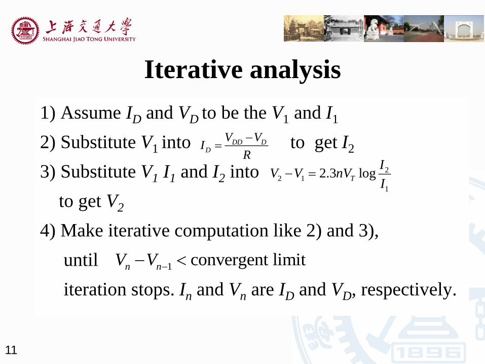
Iterative analysis
1) Assume ID and VD to be the V1 and I1
2) Substitute V1 into to get I2
3) Substitute V1 I1 and I2 into
to get V2
4) Make iterative computation like 2) and 3),
until
iteration stops. In and Vn are ID and VD, respectively.
11
DD DD
V VI
R
22 1
1
2.3 logT
IV V nV
I
1 convergent limitn nV V

4. Diode circuit models
Large-Signal Static Model
1) Ideal model
2) The constant-voltage drop model
3) Piece-wise linear model
Small Signal Model
1) Small signal resistance
2) Depletion capacitance and junction capacitance
12

Ideal model
13
reverse biasForward bias
i
v
anode Cathode
Ideal
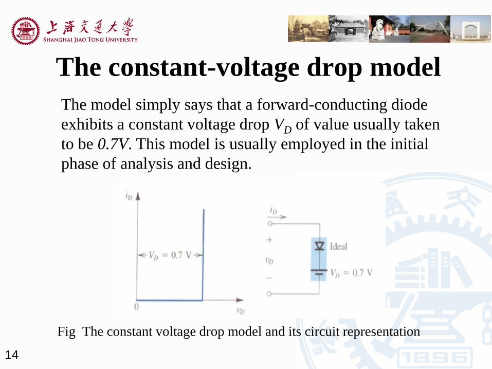
The constant-voltage drop model
14
Fig The constant voltage drop model and its circuit representation
The model simply says that a forward-conducting diode
exhibits a constant voltage drop VD of value usually taken
to be 0.7V. This model is usually employed in the initial
phase of analysis and design.

Piece-wise linear model
15
0
0 0
0,
( ) / ,
D D D
D D D D D D
i v V
i v V r v V
Fig Piecewise-linear
model of the diode
forward characteristics
and its equivalent
circuit representation
The nonlinear nature complicates the analysis of diode circuits.
For simplification, the exponential curve is approximated by
two straight lines.
Question?
How does a circuit designer to select various models?
16
This selection is a compromise between accuracy and
complexity for specific application.
The small signal model and its
application Nonlinear system to linear system- Small signal resistance
When a diode is biased to operate at a point on the forward I-V
characteristic and a small ac signal is superimposed on the dc
quantities, the diode is best modeled by a resistance equal to
the inverse of the slope of the tangent to I-V characteristic at
the bias point. This model is called diode small signal model.
17
First, we decompose the total voltage vD across the forward
biased diode into a DC voltage VD and an incremental
voltage vd, that is, defined by
D D dv V v
18
Examine effect of small signal overlapping bias:
If the amplitude of the signal vd(t) is kept sufficiently
small such that1d
T
v
kV
We may expand the exponential in a series and truncate the series
after the first two terms to make small-signal approximation.
0
( )[exp( ) 1]D d
D D d
q V vi I i I
kT
0
0
0 0
[exp( )exp( ) 1]
[exp( )(1 ) 1]
[exp( ) 1] exp( )( )
dDD d
dD
dD D
qvqVI i I
kT kT
qvqVI
kT kT
qvqV qVI I
kT kT kT
19
The total current= the dc current +the ac current (small signal)
( )D D di t I i
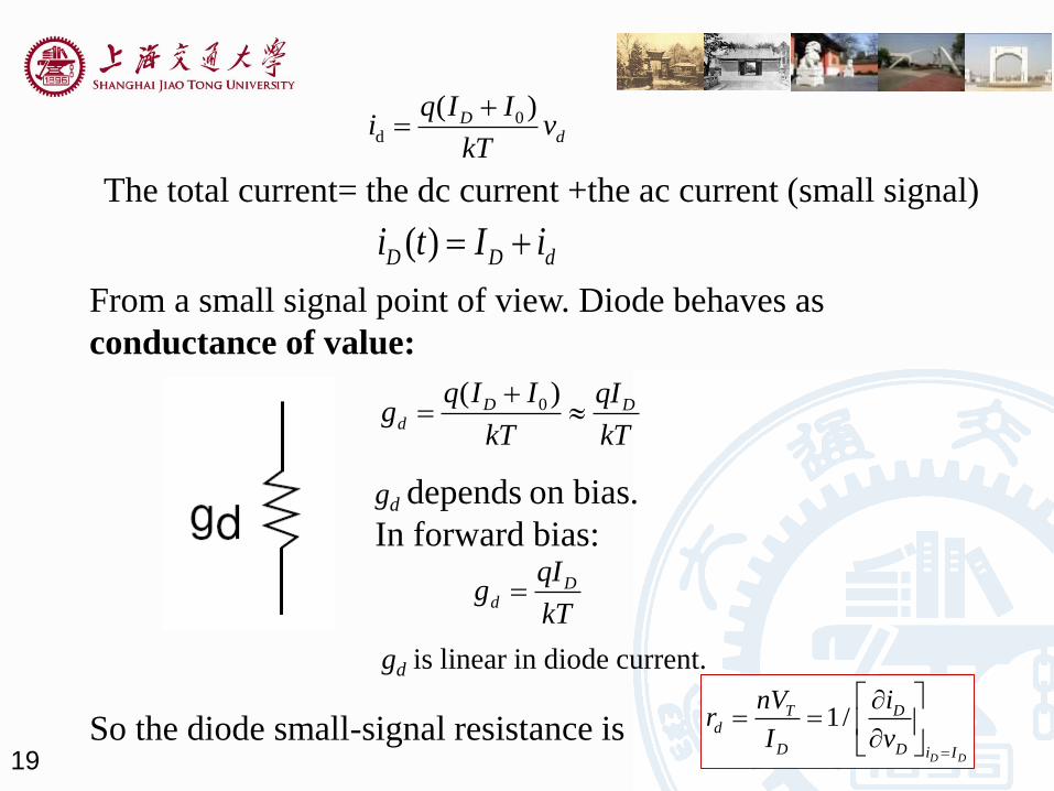
From a small signal point of view. Diode behaves as
conductance of value:
gd depends on bias.
In forward bias:
gd is linear in diode current.
So the diode small-signal resistance is 1/
D D
T Dd
D D i I
nV ir
I v
0d
( )Dd
q I Ii v
kT
0( )D Dd
q I I qIg
kT kT
Dd
qIg
kT
20
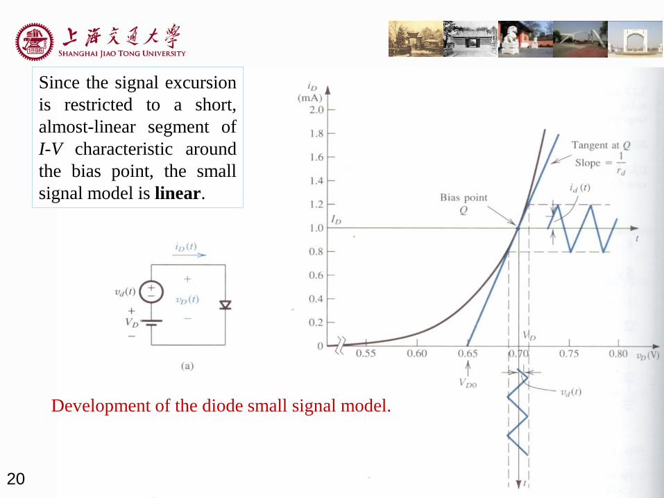
Development of the diode small signal model.
Since the signal excursion
is restricted to a short,
almost-linear segment of
I-V characteristic around
the bias point, the small
signal model is linear.
21
The small signal approximation allows us to separate
the dc analysis from the ac signal analysis.
DC analysis: 0DD D D D D D dV I R V I R V I r
VD0 is the dc point of the diode.
AC analysis: s d d dv i R i r
The signal analysis is performed by eliminating all dc
sources and replacing the diode with its small signal
resistance rd.
Small signal model is like piece-wise linear model.

22Fig The analysis of the diode circuit.
Diode circuitIts equivalent model
DC analysis AC analysis
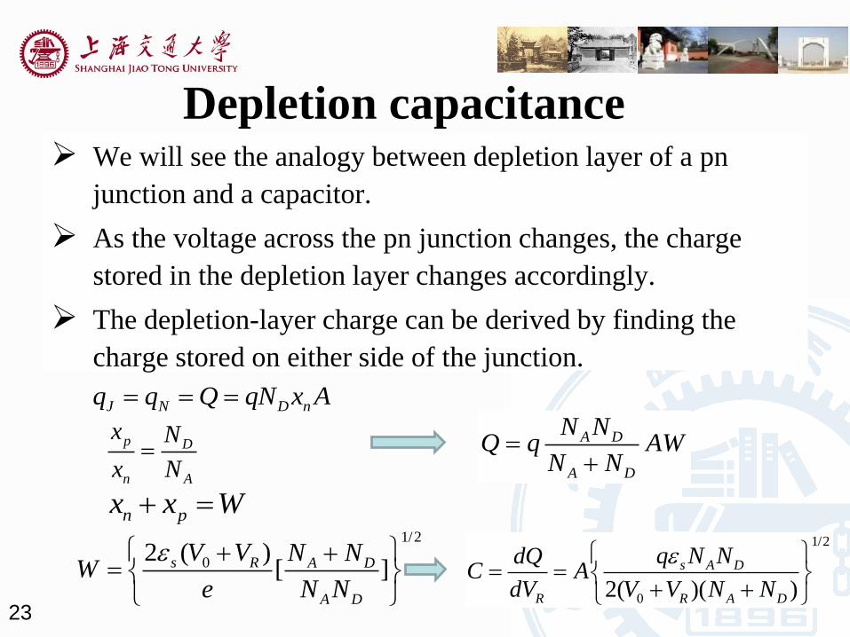
Depletion capacitance We will see the analogy between depletion layer of a pn
junction and a capacitor.
As the voltage across the pn junction changes, the charge
stored in the depletion layer changes accordingly.
The depletion-layer charge can be derived by finding the
charge stored on either side of the junction.
23
J N D nq q Q qN x A
p D
n A
x N
x N
n px x W 1/2
02( )( )
s A D
R R A D
q N NdQC A
dV V V N N
A D
A D
N NQ q AW
N N
1/2
02 ( )[ ]s R A D
A D
V V N NW
e N N

24
With bias voltage across the diode,
0
2 1 1( )( )si
D
A D
W V Vq N N
We can treat the depletion layer as parallel-plate capacitor and
the junction capacitance is
0
0
1
jsij
D
CAC
W V
V
0
0
1
2
si A Dj
A D
q N NC A
N N V
Cj0 is the zero-voltage junction capacitance.
D RV V
25
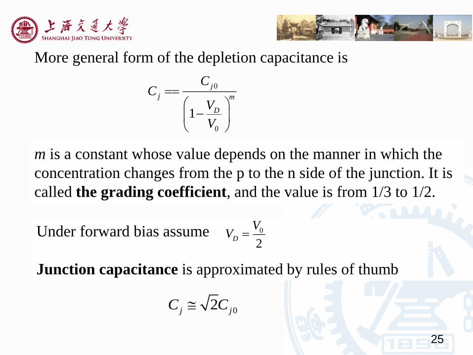
More general form of the depletion capacitance is
0
0
1
j
j m
D
CC
V
V
m is a constant whose value depends on the manner in which the
concentration changes from the p to the n side of the junction. It is
called the grading coefficient, and the value is from 1/3 to 1/2.
Under forward bias assume
Junction capacitance is approximated by rules of thumb
02j jC C
0
2D
VV
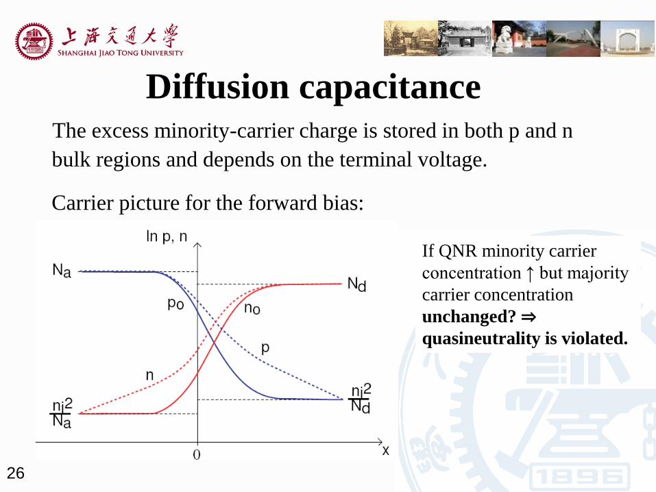
Diffusion capacitanceThe excess minority-carrier charge is stored in both p and n
bulk regions and depends on the terminal voltage.
26
Carrier picture for the forward bias:
If QNR minority carrier
concentration ↑ but majority
carrier concentration
unchanged? ⇒quasineutrality is violated.

27
Quasineutrality demands that at every point in QNR:
Excess minority carrier concentration
=excess majority carrier concentration
28
In n-type Si, at every x:
In p-type Si, at every x:
Mathematically:
0 0( ) ( )n n n np x p n x n
0 0( )p p p pn x n p x p
' '
0 0( ) ( ) ( ) ( )n nn n n np x p x p n x n x n
29
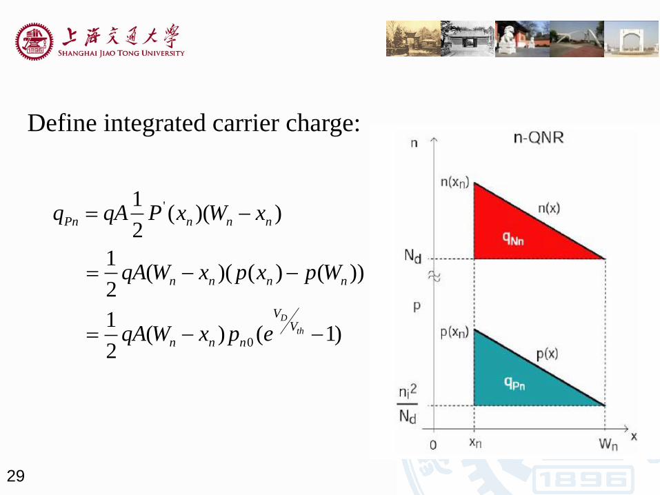
Define integrated carrier charge:
'
0
1( )( )
2
1 ( )( ( ) ( ))
2
1 ( ) ( 1)
2
D
th
Pn n n n
n n n n
VV
n n n
q qA P x W x
qA W x p x p W
qA W x p e
30
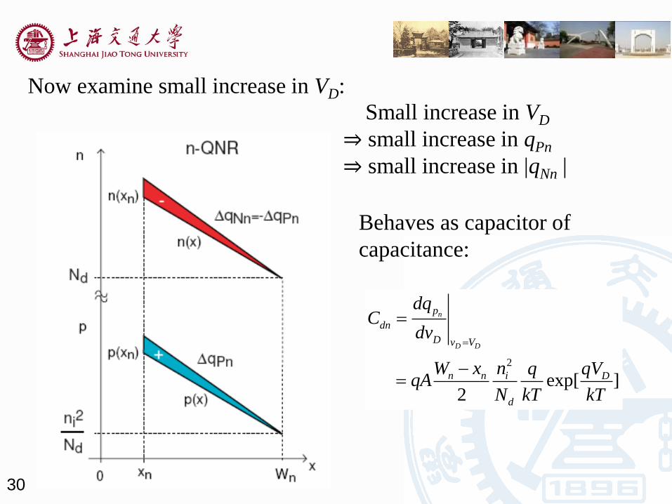
Now examine small increase in VD:
Small increase in VD
⇒ small increase in qPn
⇒ small increase in |qNn |
Behaves as capacitor of
capacitance:
2
exp[ ]2
n
D D
p
dn
D v V
n n i D
d
dqC
dv
W x n qVqqA
N kT kT
31
The total diffusion capacitance Cd is the sum of the diffusion
capacitance in n-QNR and p-QNR:
/
0 0 ( ) ( )2
p n
DD
D th
n p
d
D D vv
v V
p p p n n n
th
dq dqC
dv dv
qAW x n W x p e
V
Under forward bias, the diffusion capacitance increases
exponentially with the forward bias voltage.
Under reverse bias, the diffusion capacitance is nearly
zero. This agrees with the reverse-bias carrier distribution
which represent a tiny charge storage that furthermore is
not a function of the diode voltage.
32
Can write in terms of IDp (portion of diode current due to
holes in nQNR):
Define transit time of holes through nQNR:
Transit time is the average time for a hole to diffuse through
nQNR
2
exp[ 1]( )
pi Dp
d n n
Dn qVJ q
N W x kT
2 2
2
( )exp[ ]
2 ( )
( )
2
pn n i Ddn
p d n n
n nDp
p
DW x n qVqC qA
kT D N W x kT
W xqI
kT D
33
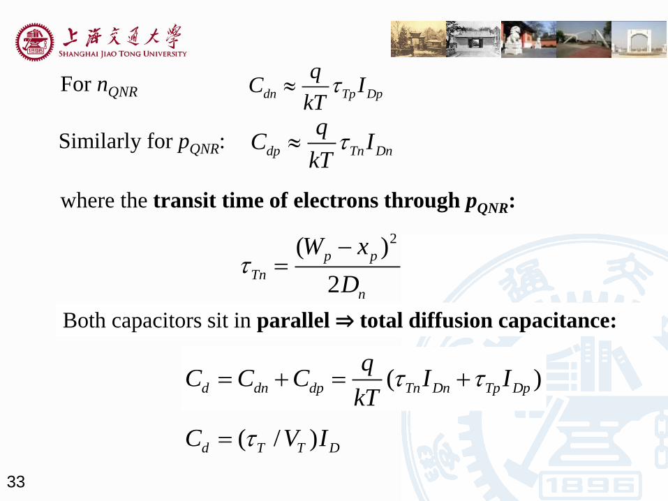
Similarly for pQNR:
For nQNR
where the transit time of electrons through pQNR:
Both capacitors sit in parallel ⇒ total diffusion capacitance:
( / )d T T DC V I
( )d dn dp Tn Dn Tp Dp
qC C C I I
kT
2( )
2
p p
Tn
n
W x
D
dp Tn Dn
qC I
kT
dn Tp Dp
qC I
kT
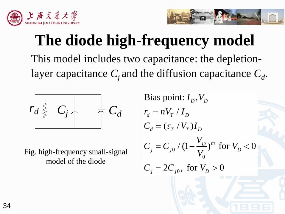
The diode high-frequency modelThis model includes two capacitance: the depletion-
layer capacitance Cj and the diffusion capacitance Cd.
34
rd Cj Cd
Fig. high-frequency small-signal
model of the diode
0
0
0
Bias point: ,
/
( / )
/ (1 ) for 0
2 , for 0
D D
d T D
d T T D
mDj j D
j j D
I V
r nV I
C V I
VC C V
V
C C V
35
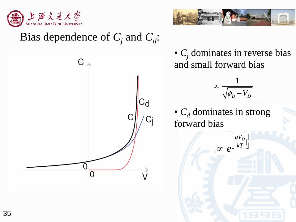
Bias dependence of Cj and Cd:
• Cj dominates in reverse bias
and small forward bias
• Cd dominates in strong
forward bias
DqV
kTe
1
B DV

Summary of small-signal model
36
• Diode Current:
• Conductance: associated with current voltage characteristics
– gd∝ I in forward bias,
– gd negligible in reverse bias
• Junction capacitance: associated with charge modulation
in depletion region
• Diffusion capacitance: associated with charge storage in
QNRs to maintain quasineutrality.
0 1DqV
kTI I e
1j
B D
CV
DqV
kT
dC e
37
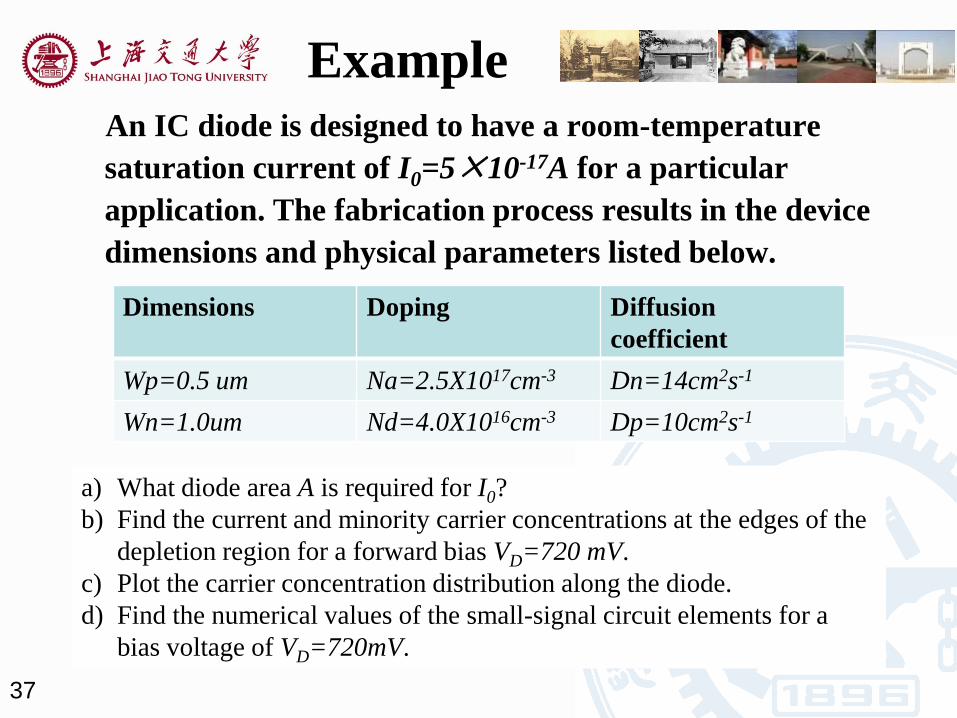
ExampleAn IC diode is designed to have a room-temperature
saturation current of I0=5×10-17A for a particular
application. The fabrication process results in the device
dimensions and physical parameters listed below.
Dimensions Doping Diffusion
coefficient
Wp=0.5 um Na=2.5X1017cm-3 Dn=14cm2s-1
Wn=1.0um Nd=4.0X1016cm-3 Dp=10cm2s-1
a) What diode area A is required for I0?
b) Find the current and minority carrier concentrations at the edges of the
depletion region for a forward bias VD=720 mV.
c) Plot the carrier concentration distribution along the diode.
d) Find the numerical values of the small-signal circuit elements for a
bias voltage of VD=720mV.
38
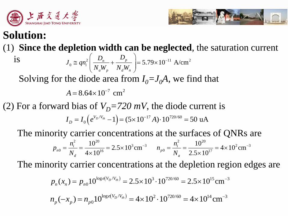
Solution:(1) Since the depletion width can be neglected, the saturation current
is 2 11 2
0 5.79 10 A/cmpn
i
a p d n
DDJ qn
N W N W
Solving for the diode area from I0=J0A, we find that7 28.64 10 cmA
(2) For a forward bias of VD=720 mV, the diode current is
/ 17 720/60
0 1 (5 10 ) 10 50 uAD thV V
DI I e A
The minority carrier concentrations at the surfaces of QNRs are2 20
3 3
0 16
102.5 10 cm
4 10
in
d
np
N
2 202 3
0 17
104 10 cm
2.5 10
ip
a
nn
N
The minority carrier concentrations at the depletion region edges are
log / 3 720/60 15 3
0( ) 10 2.5 10 10 2.5 10 cmD the V V
n n np x p
log / 2 720/60 14 3
0( ) 10 4 10 10 4 10 cmD the V V
p p pn x n
39
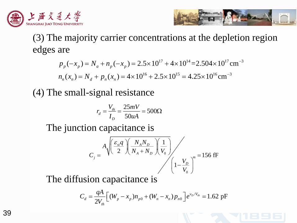
(3) The majority carrier concentrations at the depletion region
edges are17 14 17 3
16 15 16 3
( ) ( ) 2.5 10 4 10 =2.504 10 cm
( ) ( ) 4 10 2.5 10 4.25 10 cm
p p a p p
n n d n n
p x N n x
n x N p x
(4) The small-signal resistance
25500
50
thd
D
V mVr
I uA
0
0
1
2156 fF
1
si A D
A Dmj
D
q N NA
N N VC
V
V
The junction capacitance is
/
0 0( ) ( ) 1.62 pF2
D thv V
d p p p n n n
th
qAC W x n W x p e
V
The diffusion capacitance is

Homework 13
7
0 10n s 8
0 10p s 210cm /pD s 225cm /nD s
Assume the width of QNR regions are much larger than the width of the
depletion region.

5. The application of diodes
Voltage regulator
Rectifier
Limiting and clamping circuit
41
42
Use of the diode forward drop in
voltage regulation (稳压器) What is voltage regulator?
A voltage regulator is a circuit to provide a constant dc voltage
between its output terminals in spite of
(a) changes in the load current drawn from the regulator output
terminal
(b) changes in the dc power-supply voltage that feeds the regulator.
Why can the diode be used in voltage regulator?
The forward voltage drop of the diode remains almost constant at
approximately 0.7V while the current through it varies relatively
large amounts.
43
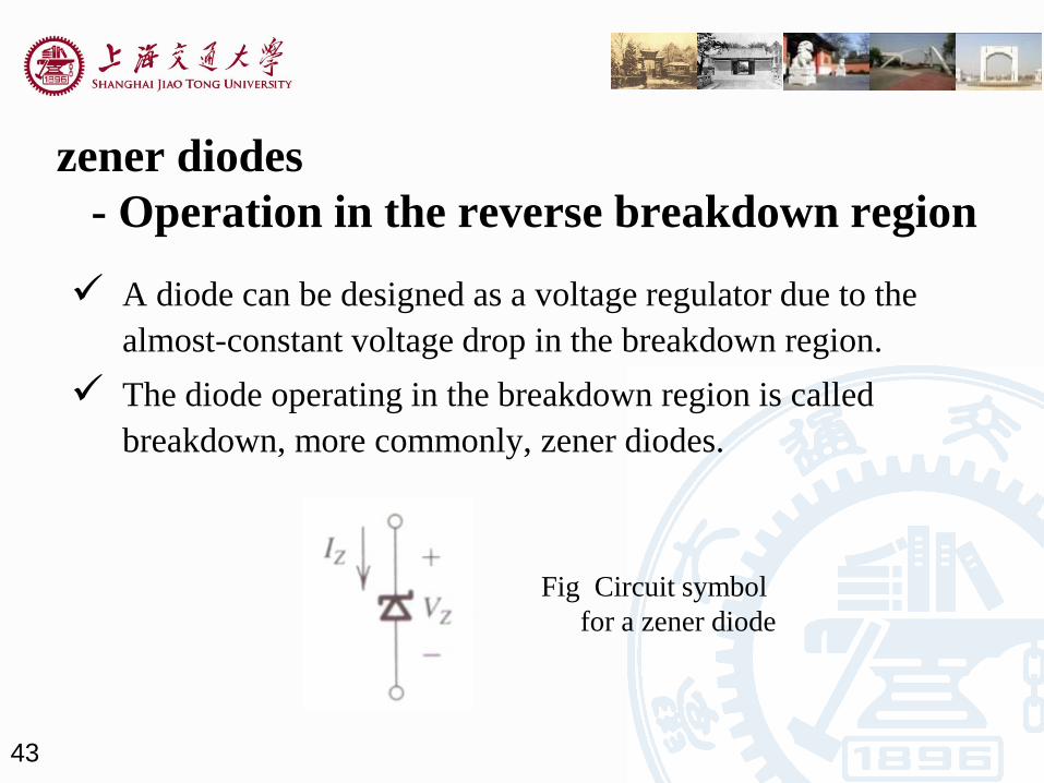
zener diodes
- Operation in the reverse breakdown region
A diode can be designed as a voltage regulator due to the
almost-constant voltage drop in the breakdown region.
The diode operating in the breakdown region is called
breakdown, more commonly, zener diodes.
Fig Circuit symbol
for a zener diode
44
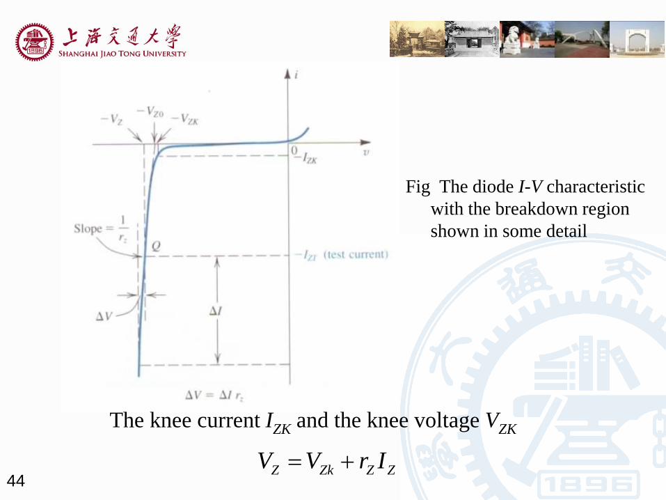
The knee current IZK and the knee voltage VZK
Z Zk Z ZV V r I
Fig The diode I-V characteristic
with the breakdown region
shown in some detail
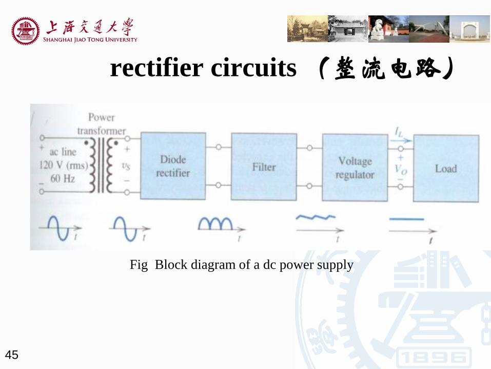
rectifier circuits (整流电路)
45
Fig Block diagram of a dc power supply
46
The diode rectifier converts the input sinusoid vs to a unipolar
output, which has a dc component.
Filter is used to reduce the variation of the magnitude.
Finally the voltage regulator is employed to reduce ripple and
stabilize the magnitude of the dc output voltage against variation
caused by changes in load current.
power transformer
- consists of two separated coils would around an iron core that
magnetically couples the two windings.
- The primary winding has N1 turns, and the second winding
has N2 turns. 2120
1s
Nv V
N
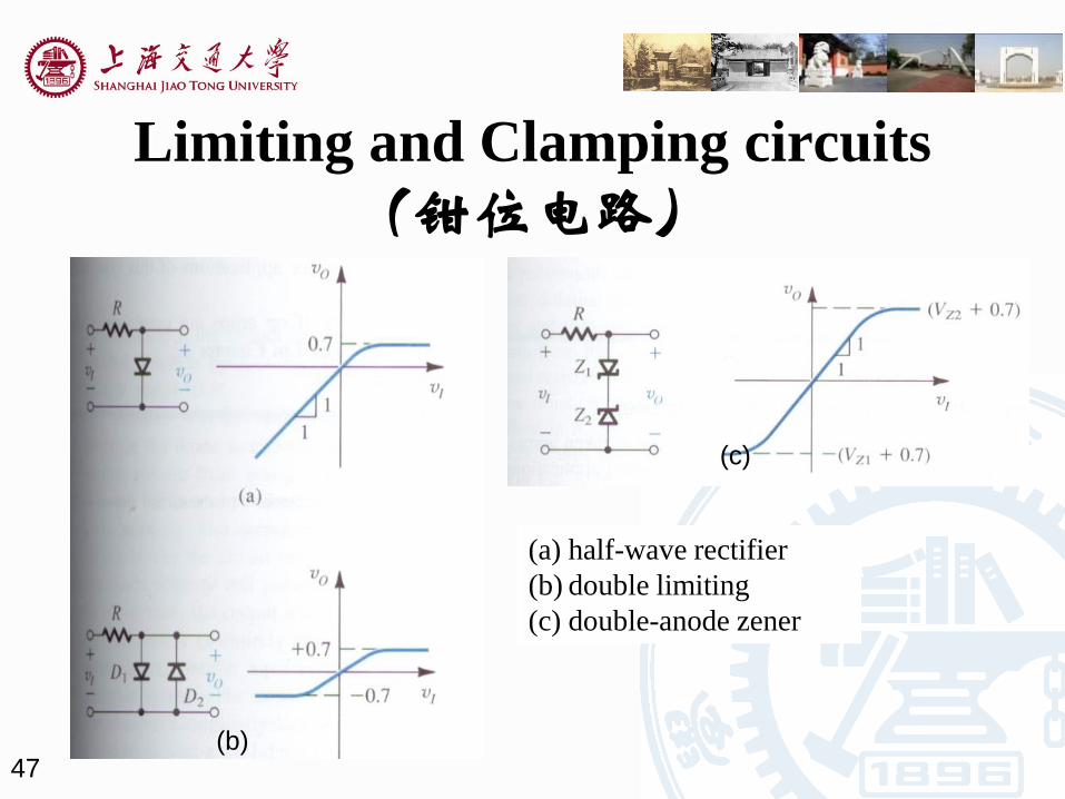
Limiting and Clamping circuits
(钳位电路)
47
(a) half-wave rectifier
(b) double limiting
(c) double-anode zener
(b)
(c)

48
6. Special diodes types
The Schottky-barrier diode (SBD) 肖特基势垒二极管
It brings metal into contact with a moderately doped n-type semiconductor material.
The resulting metal-semiconductor junction behaves like a diode.
Two applications: 1) Gallium Arsenide (GaAs) circuits;
2) bipolar-transistor logic circuits.
Varactors (voltage-variable capacitors)
Reverse-biased pn junctions exhibit a charge-storage effect that is modeled with the
depletion-layer or junction capacitance Cj, which is a function of the reverse-biased
voltage VR.
Photodiodes
A photodiode can be use to convert light signal into electrical signals.
It is an important component of optoelectronics or photonics.
Light-Emitting Diodes (LEDs)
It converts a forward current into lights, as a inverse function of the photodiode.

7 . The SPICE diode model and
simulation
49
The capacitance, cd, is a combination of diffusion capacitance,
(cdiff), depletion capacitance, (cdep), metal, (cmetal), and poly
capacitances, (cpoly). cd cdiff cdep cmetal cpoly
( 1)vd
N vtid ISeff e

50
.MODEL mname D <LEVEL = val> <keyword = val> ...
mname Model name. The diode element refers to the
model by this name.
D Symbol that identifies a diode model
LEVEL Symbol that identifies a diode model
LEVEL=1 =junction diode
LEVEL=2 =Fowler-Nordheim
LEVEL=3 =geometric processing for junction diode

51
2 pn
s i
d n na p p
DDI qAn
N W xN W x
0
0
1
2
si A Dj
A D
q N NC A
N N V
2ln( )a d
B
i
N NkT
q n
2( )
2
n nTp
p
W x
D

52

53
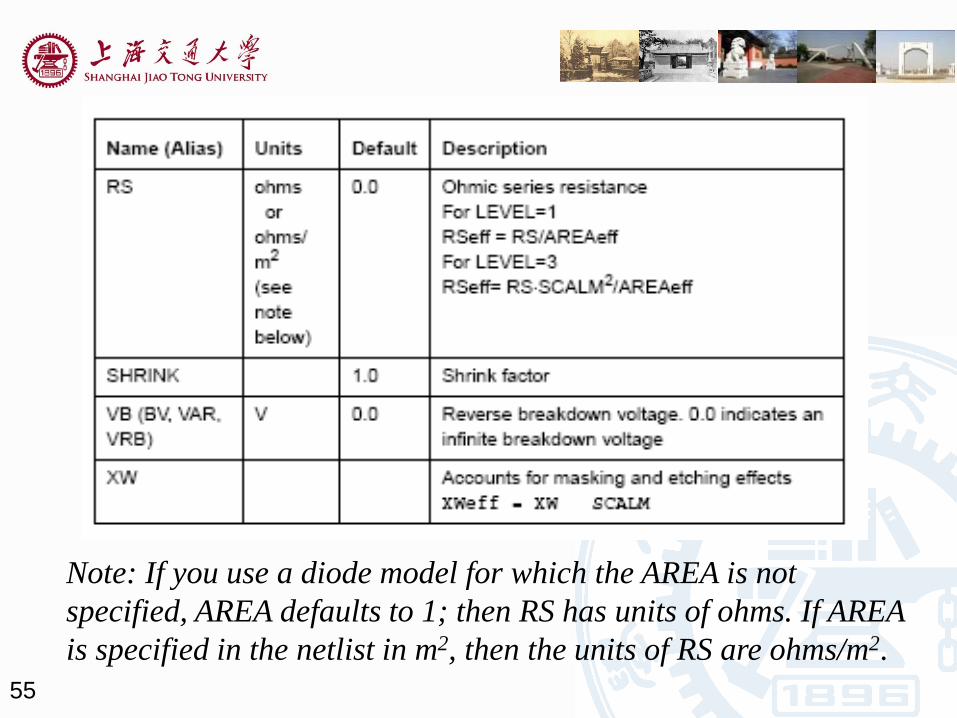
Setting Junction DC Parameters in Level 1 and 3

54
55
Note: If you use a diode model for which the AREA is not
specified, AREA defaults to 1; then RS has units of ohms. If AREA
is specified in the netlist in m2, then the units of RS are ohms/m2.
56
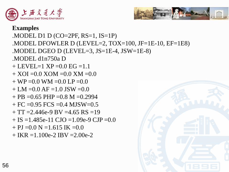
Examples
.MODEL D1 D (CO=2PF, RS=1, IS=1P)
.MODEL DFOWLER D (LEVEL=2, TOX=100, JF=1E-10, EF=1E8)
.MODEL DGEO D (LEVEL=3, JS=1E-4, JSW=1E-8)
.MODEL d1n750a D
+ LEVEL=1 XP =0.0 EG =1.1
+ XOI =0.0 XOM =0.0 XM =0.0
+ WP =0.0 WM =0.0 LP =0.0
+ LM =0.0 AF =1.0 JSW =0.0
+ PB =0.65 PHP =0.8 M =0.2994
+ FC =0.95 FCS =0.4 MJSW=0.5
+ TT =2.446e-9 BV =4.65 RS =19
+ IS =1.485e-11 CJO =1.09e-9 CJP =0.0
+ PJ =0.0 N =1.615 IK =0.0
+ IKR =1.100e-2 IBV =2.00e-2
57
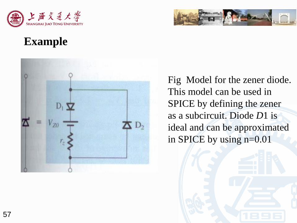
Example
Fig Model for the zener diode.
This model can be used in
SPICE by defining the zener
as a subcircuit. Diode D1 is
ideal and can be approximated
in SPICE by using n=0.01

58
* Zener diode_subcircuit
.subckt zener_diode 1 2
* anode
* cathode
Rz 3 4 10
Vz 2 3 4.9
D1 1 2 diode1
D2 1 4 diode_ideal
.model diode1 (IS=100pA n=1.679)
.model diode_ideal (IS=100pA n=0.01)
.ends zener_diode
59
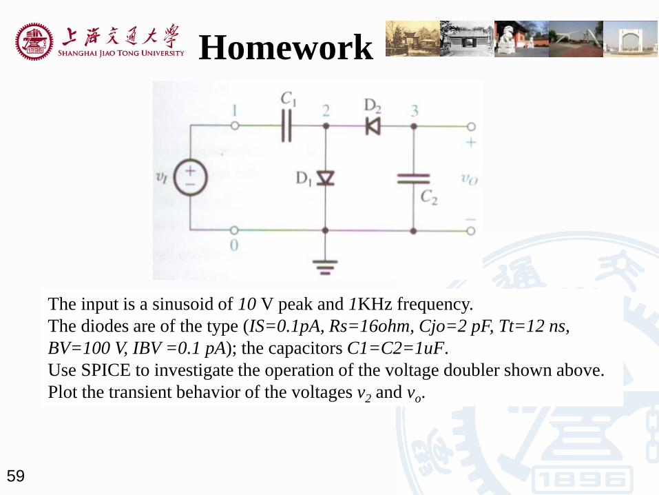
Homework
The input is a sinusoid of 10 V peak and 1KHz frequency.
The diodes are of the type (IS=0.1pA, Rs=16ohm, Cjo=2 pF, Tt=12 ns,
BV=100 V, IBV =0.1 pA); the capacitors C1=C2=1uF.
Use SPICE to investigate the operation of the voltage doubler shown above.
Plot the transient behavior of the voltages v2 and vo.