lecture 28: single stage frequency...
TRANSCRIPT
1
Department of EECS University of California, Berkeley
EECS 105 Spring 2004, Lecture 28
Lecture 28: Single Stage Frequency response
Prof J. S. Smith
Department of EECS University of California, Berkeley
EECS 105 Spring 2004, Lecture 28 Prof. J. S. Smith
Context
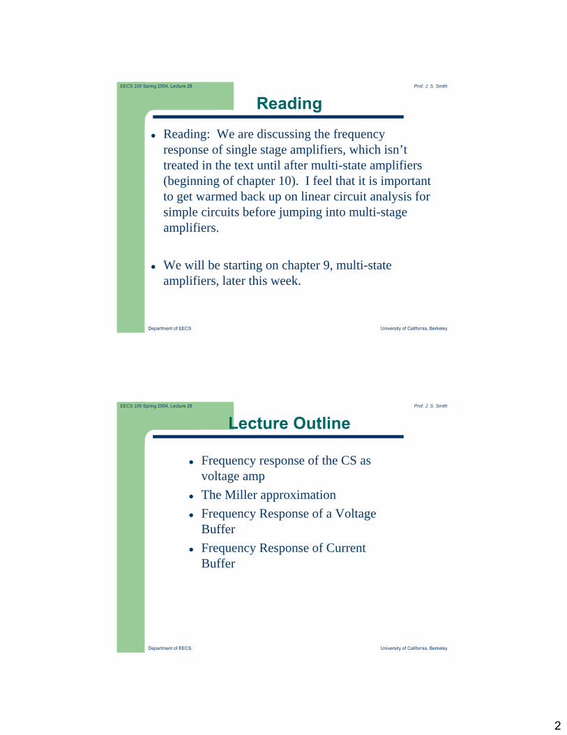
In today’s lecture, we will continue to look at the frequency response of single stage amplifiers, starting with a more complete discussion of the CS amplifier, and then looking at the frequency response of CG and the CD connections.
Next: Multi-state amplifiers
2
Department of EECS University of California, Berkeley
EECS 105 Spring 2004, Lecture 28 Prof. J. S. Smith
Reading
Reading: We are discussing the frequency response of single stage amplifiers, which isn’t treated in the text until after multi-state amplifiers (beginning of chapter 10). I feel that it is important to get warmed back up on linear circuit analysis for simple circuits before jumping into multi-stage amplifiers.
We will be starting on chapter 9, multi-state amplifiers, later this week.
Department of EECS University of California, Berkeley
EECS 105 Spring 2004, Lecture 28 Prof. J. S. Smith
Lecture Outline
Frequency response of the CS as voltage ampThe Miller approximationFrequency Response of a Voltage BufferFrequency Response of Current Buffer
3
Department of EECS University of California, Berkeley
EECS 105 Spring 2004, Lecture 28 Prof. J. S. Smith
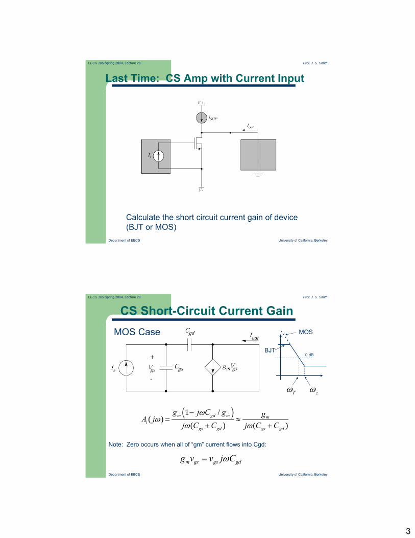
Last Time: CS Amp with Current Input
Calculate the short circuit current gain of device (BJT or MOS)
Department of EECS University of California, Berkeley
EECS 105 Spring 2004, Lecture 28 Prof. J. S. Smith
CS Short-Circuit Current Gain
( )1 /( )
( ) ( )m gd m m
igs gd gs gd
g j C g gA jj C C j C C
ωω
ω ω−
= ≈+ +
MOS Case
0 dB
MOS
BJT
Tω zω
Note: Zero occurs when all of “gm” current flows into Cgd:
m gs gs gdg v v j Cω=

4
Department of EECS University of California, Berkeley
EECS 105 Spring 2004, Lecture 28 Prof. J. S. Smith
Input impedance
Look at how Zgd affects the transfer function: find Zin
gdC
Department of EECS University of California, Berkeley
EECS 105 Spring 2004, Lecture 28 Prof. J. S. Smith
Input Impedance Zin(jω)
At output node:
gdouttt ZVVI /)( −=
outtmoutttmout RVgRIVgV ′−≈′−−= )( Why?
gdtvCtt ZVAVIgd
/)( −=
vCgd
gdttin A
ZIVZ
−==
1/
5
Department of EECS University of California, Berkeley
EECS 105 Spring 2004, Lecture 28 Prof. J. S. Smith
Miller Capacitance CM
Effective input capacitance:
( )[ ]gdvCgdgdvCMin CAjCjACj
Zgd
−=⎟
⎟⎠
⎞⎜⎜⎝
⎛⎟⎟
⎠
⎞
⎜⎜
⎝
⎛
−==
111
111
ωωω
AV,Cx
+
─
+
─
VinVout
Cx
AV,Cx
+
─
+
─Vout
(1-Av,Cx)Cx
(1-1/Av,Cx)Cx
Department of EECS University of California, Berkeley
EECS 105 Spring 2004, Lecture 28 Prof. J. S. Smith
Some Examples
Common source (emitter) amplifier:
=gdvCA Negative, large number (-100)
Common drain (collector) amplifier:
=gsvCA Slightly less than 1
→Miller Multiplied Cap has Detrimental Impact on bandwidth
“Bootstrapped” cap has negligible impact on bandwidth!
( ) gdgdCVM CCACgd
1001 , ≈−=
( ) gsgsCVM CCACgs
01 , ≈−=
6
Department of EECS University of California, Berkeley
EECS 105 Spring 2004, Lecture 28 Prof. J. S. Smith
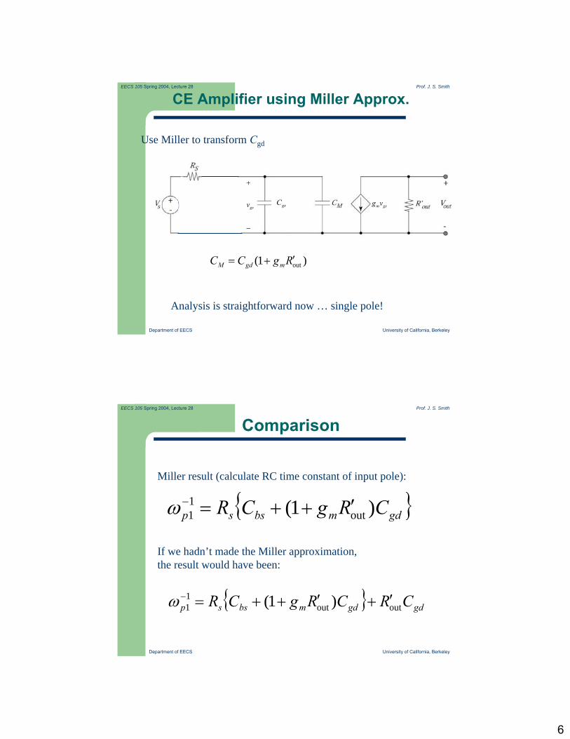
CE Amplifier using Miller Approx.
Use Miller to transform Cgd
Analysis is straightforward now … single pole!
−
+
gsv gsC gsmvg
)1( outRgCC mgdM ′+=
Department of EECS University of California, Berkeley
EECS 105 Spring 2004, Lecture 28 Prof. J. S. Smith
Comparison
Miller result (calculate RC time constant of input pole):
If we hadn’t made the Miller approximation, the result would have been:
{ }gdmbssp CRgCR )1( out11 ′++=−ω
{ } gdgdmbssp CRCRgCR outout11 )1( ′+′++=−ω
7
Department of EECS University of California, Berkeley
EECS 105 Spring 2004, Lecture 28 Prof. J. S. Smith
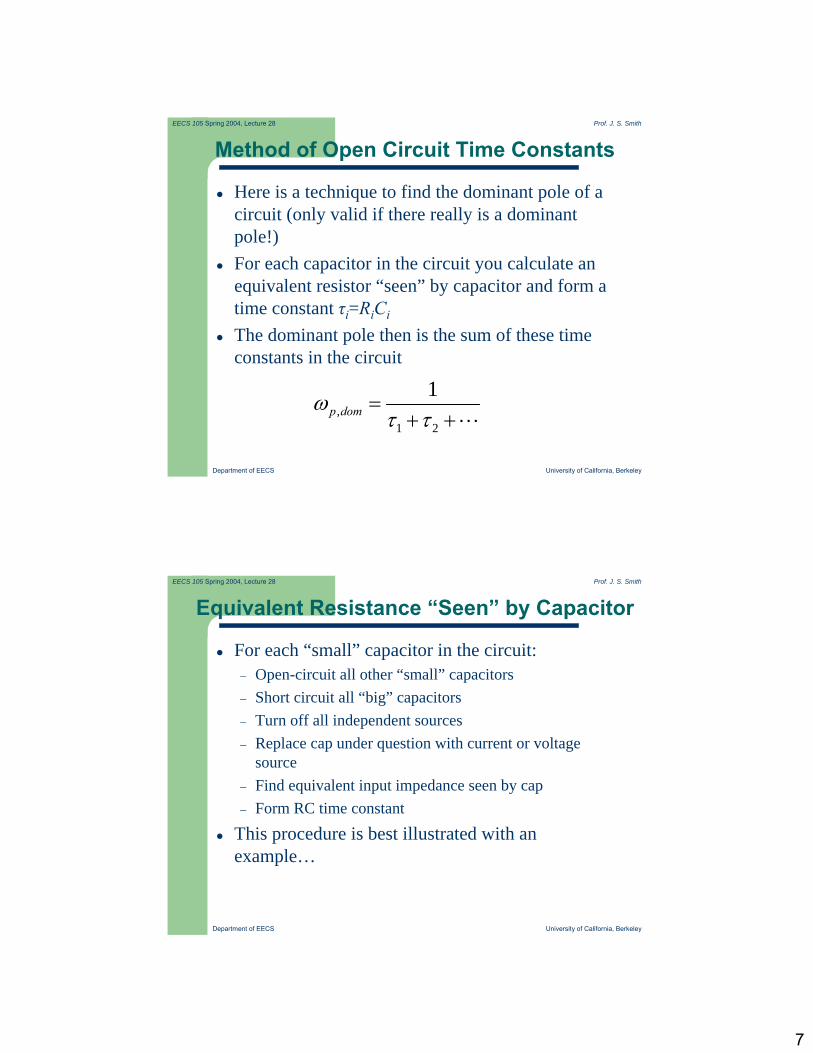
Method of Open Circuit Time Constants
Here is a technique to find the dominant pole of a circuit (only valid if there really is a dominant pole!)For each capacitor in the circuit you calculate an equivalent resistor “seen” by capacitor and form a time constant τi=RiCi
The dominant pole then is the sum of these time constants in the circuit
,1 2
1p domω
τ τ=
+ +L
Department of EECS University of California, Berkeley
EECS 105 Spring 2004, Lecture 28 Prof. J. S. Smith
Equivalent Resistance “Seen” by Capacitor
For each “small” capacitor in the circuit:– Open-circuit all other “small” capacitors– Short circuit all “big” capacitors– Turn off all independent sources– Replace cap under question with current or voltage
source– Find equivalent input impedance seen by cap– Form RC time constant
This procedure is best illustrated with an example…

8
Department of EECS University of California, Berkeley
EECS 105 Spring 2004, Lecture 28 Prof. J. S. SmithExample Calculation: CE input impedance
Consider the input capacitanceOpen all other “small” caps (get rid of output cap)Turn off all independent sourcesInsert a current source in place of cap and find impedance seen by source
1 MC C Cπ= +
||M SR r Rπ=
( ) ( ){ }1 || 1S m outR r C g R Cπ π µτ ′= + +
Department of EECS University of California, Berkeley
EECS 105 Spring 2004, Lecture 28 Prof. J. S. Smith
Common-Drain Amplifier
21 ( )2DS ox GS T
WI C V VL
µ= −
2 DSGS T
ox
IV V WCL
µ= +
Weak IDS dependence

9
Department of EECS University of California, Berkeley
EECS 105 Spring 2004, Lecture 28 Prof. J. S. Smith
CD Voltage Gain
1out m
in mb m
v gv g g
≈ ≈+
Department of EECS University of California, Berkeley
EECS 105 Spring 2004, Lecture 28 Prof. J. S. Smith
CD Output Resistance
Sum currents at output (source) node:
|| || tout o oc
t
vR r ri
= t m t mb ti g v g v= +
1out
m mb
Rg g
≈+
10
Department of EECS University of California, Berkeley
EECS 105 Spring 2004, Lecture 28 Prof. J. S. Smith
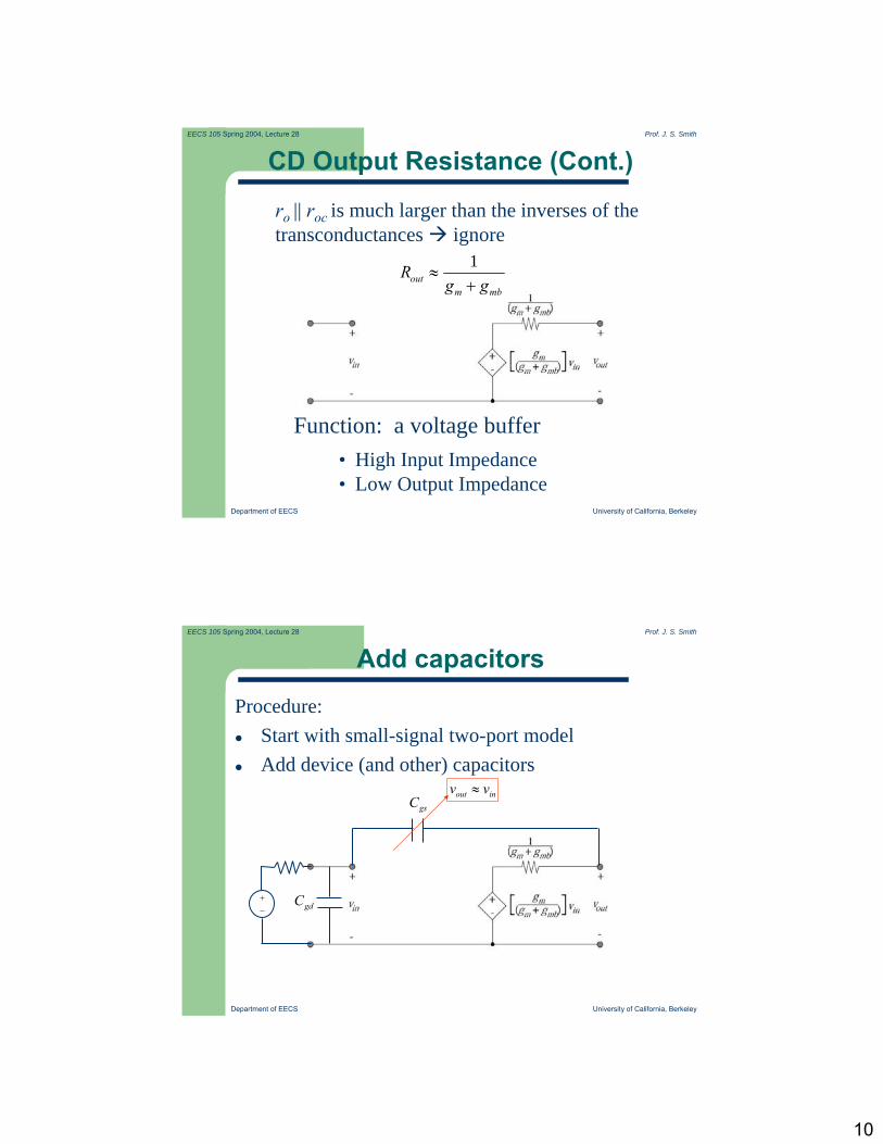
CD Output Resistance (Cont.)
ro || roc is much larger than the inverses of the transconductances ignore
1out
m mb
Rg g
≈+
Function: a voltage buffer• High Input Impedance• Low Output Impedance
Department of EECS University of California, Berkeley
EECS 105 Spring 2004, Lecture 28 Prof. J. S. Smith
Add capacitors
Procedure:Start with small-signal two-port modelAdd device (and other) capacitors
gdC
gsC
−+
inout vv ≈

11
Department of EECS University of California, Berkeley
EECS 105 Spring 2004, Lecture 28 Prof. J. S. Smith
Common-Collector Amplifier
Department of EECS University of California, Berkeley
EECS 105 Spring 2004, Lecture 28 Prof. J. S. Smith
Two-Port CC Model with Capacitors
Find Miller capacitor for Cπ -- note that the base-emitter capacitor is between the input and output
Gain ~ 1
12
Department of EECS University of California, Berkeley
EECS 105 Spring 2004, Lecture 28 Prof. J. S. Smith
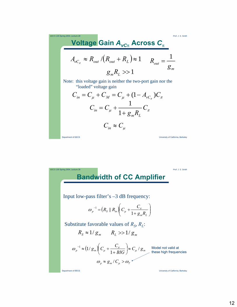
Voltage Gain AvCπ Across Cπ
Note: this voltage gain is neither the two-port gain nor the “loaded” voltage gain
πµµ πCACCCC vCMin )1( −+=+=
11in
m L
C C Cg Rµ π= +
+
inC Cµ≈
1out
m
Rg
=
1m Lg R >>
( ) 1/ ≈+≈ LoutoutC RRRAπν
Department of EECS University of California, Berkeley
EECS 105 Spring 2004, Lecture 28 Prof. J. S. Smith
Bandwidth of CC Amplifier
Input low-pass filter’s –3 dB frequency:
( ) ⎟⎟⎠
⎞⎜⎜⎝
⎛+
+=−
LminSp Rg
CCRR1
||1 πµω
Substitute favorable values of RS, RL:
mS gR /1≈ mL gR /1>>
( ) mmp gCBIG
CCg /1
/11µ
πµω ≈⎟
⎠⎞
⎜⎝⎛
++≈−
/p m Tg Cµω ω≈ >
Model not valid at these high frequencies
13
Department of EECS University of California, Berkeley
EECS 105 Spring 2004, Lecture 28 Prof. J. S. Smith
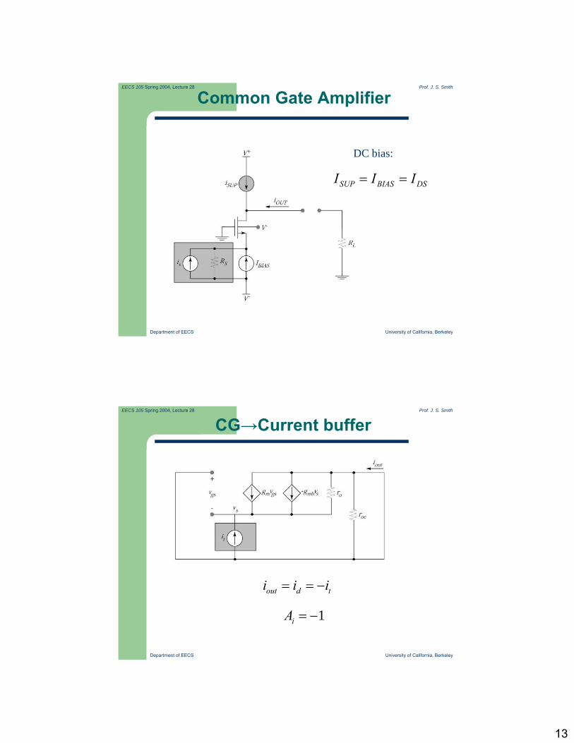
Common Gate Amplifier
DC bias:
SUP BIAS DSI I I= =
Department of EECS University of California, Berkeley
EECS 105 Spring 2004, Lecture 28 Prof. J. S. Smith
CG→Current buffer
out d ti i i= = −
1iA = −
14
Department of EECS University of California, Berkeley
EECS 105 Spring 2004, Lecture 28 Prof. J. S. Smith
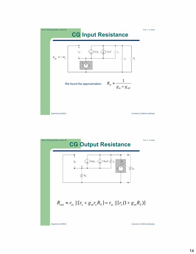
CG Input Resistance
gs tv v= −
mbmin gg
R+
≈1
We found the approximation:
Department of EECS University of California, Berkeley
EECS 105 Spring 2004, Lecture 28 Prof. J. S. Smith
CG Output Resistance
)]1([||][|| SmoocSomoocout RgrrRrgrrR +=+≈
15
Department of EECS University of California, Berkeley
EECS 105 Spring 2004, Lecture 28 Prof. J. S. Smith
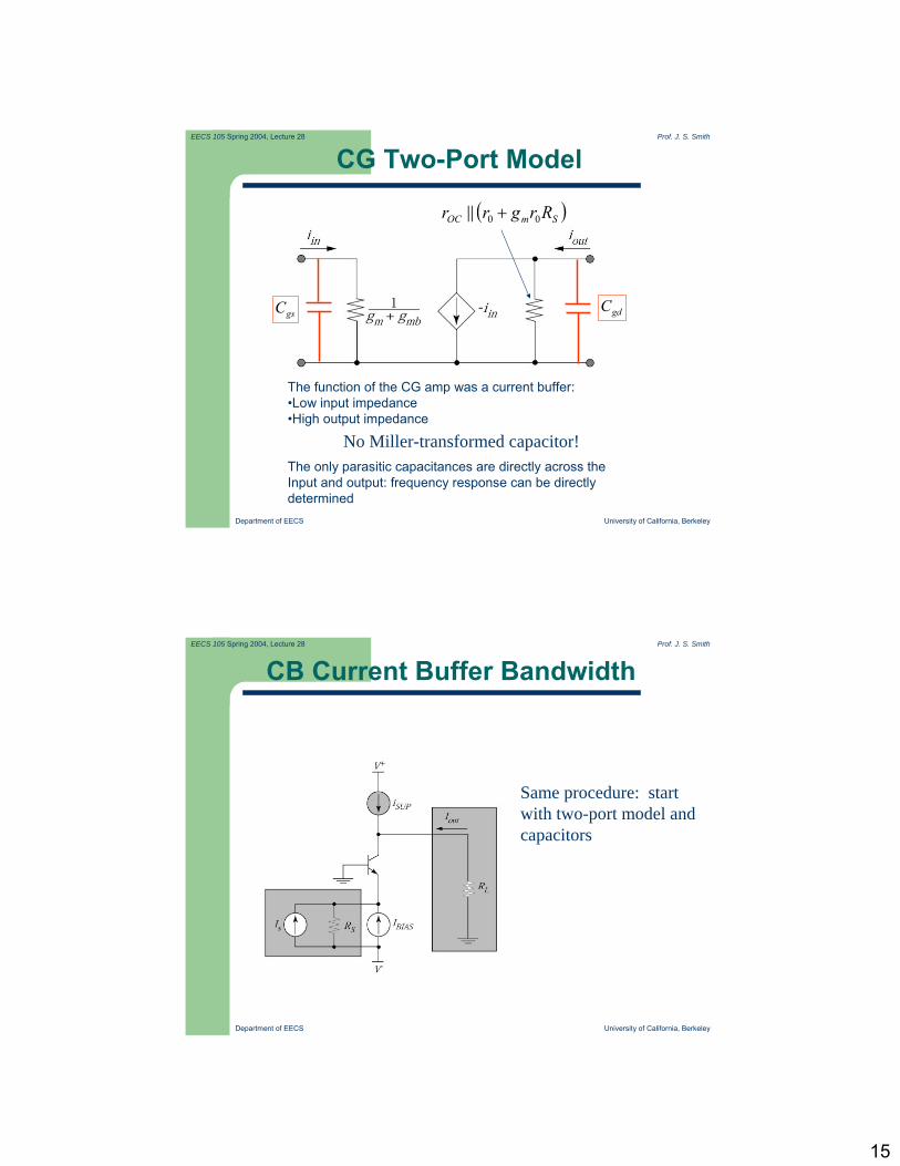
CG Two-Port Model
The function of the CG amp was a current buffer:•Low input impedance•High output impedance
The only parasitic capacitances are directly across theInput and output: frequency response can be directlydetermined
( )SmOC Rrgrr 00|| +
gsC gdC
No Miller-transformed capacitor!
Department of EECS University of California, Berkeley
EECS 105 Spring 2004, Lecture 28 Prof. J. S. Smith
CB Current Buffer Bandwidth
Same procedure: startwith two-port model andcapacitors

16
Department of EECS University of California, Berkeley
EECS 105 Spring 2004, Lecture 28 Prof. J. S. Smith
Two-Port CB Model with Capacitors
Unity-gain frequency is on the order of ωT for small RL
No Miller-transformed capacitor!
Department of EECS University of California, Berkeley
EECS 105 Spring 2004, Lecture 28 Prof. J. S. SmithSummation of Single-Stage Amp Frequency Response
CS, CE: suffer from Miller-magnified capacitor for high-gain caseCD, CC: Miller transformation nulledcapacitor “wideband stage”CG, CB: no Millerized capacitor wideband stage (for low load resistance)