lecture 23: multistage amps-cascades and cascodesee105/fa03/handouts/lectures/... · department of...
TRANSCRIPT
Department of EECS University of California, Berkeley
EECS 105 Fall 2003, Lecture 23
Lecture 23:Multistage Amps-Cascades and
Cascodes
Prof. Niknejad
Department of EECS University of California, Berkeley
EECS 105 Fall 2003, Lecture 23 Prof. A. Niknejad
Lecture Outline
Example 1: Cascodes Amp Design
Example 2: Two Stage CS Amp
Department of EECS University of California, Berkeley
EECS 105 Fall 2003, Lecture 23 Prof. A. Niknejad
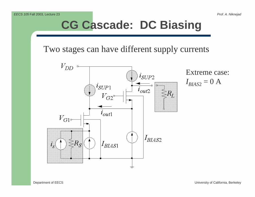
CG Cascade: DC Biasing
Two stages can have different supply currents
Extreme case:IBIAS2 = 0 A

Department of EECS University of California, Berkeley
EECS 105 Fall 2003, Lecture 23 Prof. A. Niknejad
CG Cascade: Sharing a Supply
First stage has no currentsupply of its own its outputresistance is modified
Department of EECS University of California, Berkeley
EECS 105 Fall 2003, Lecture 23 Prof. A. Niknejad
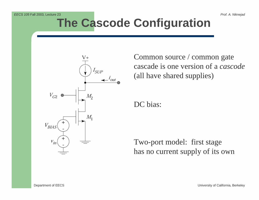
The Cascode Configuration
DC bias:
Two-port model: first stage has no current supply of its own
Common source / common gatecascade is one version of a cascode(all have shared supplies)
Department of EECS University of California, Berkeley
EECS 105 Fall 2003, Lecture 23 Prof. A. Niknejad
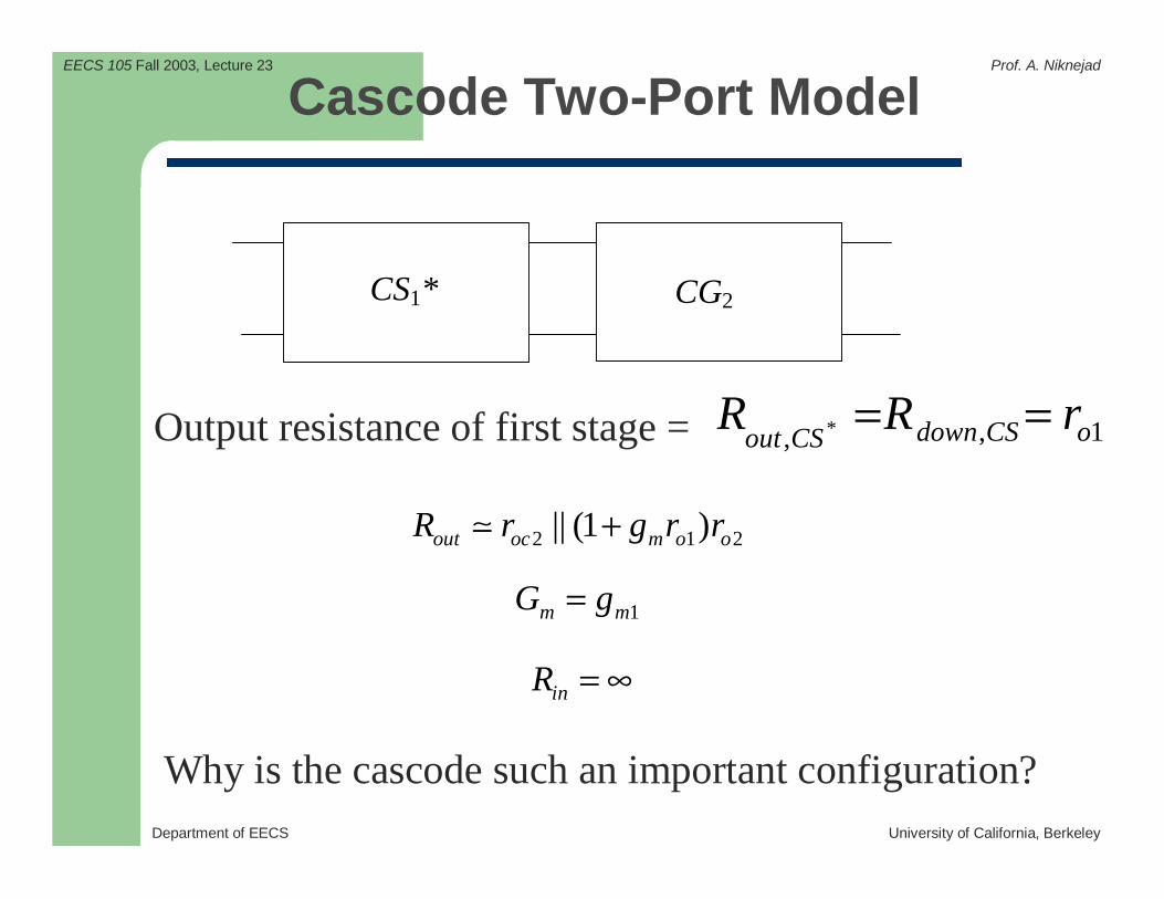
Cascode Two-Port Model
CS1* CG2
Output resistance of first stage = 1,, * oCSdownCSoutrRR ==
Why is the cascode such an important configuration?
2 1 2|| (1 )out oc m o oR r g r r+
1m mG g=
inR = ∞
Department of EECS University of California, Berkeley
EECS 105 Fall 2003, Lecture 23 Prof. A. Niknejad
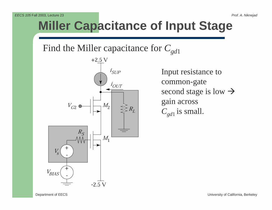
Miller Capacitance of Input Stage
Find the Miller capacitance for Cgd1
Input resistance to common-gatesecond stage is low gain acrossCgd1 is small.
Department of EECS University of California, Berkeley
EECS 105 Fall 2003, Lecture 23 Prof. A. Niknejad
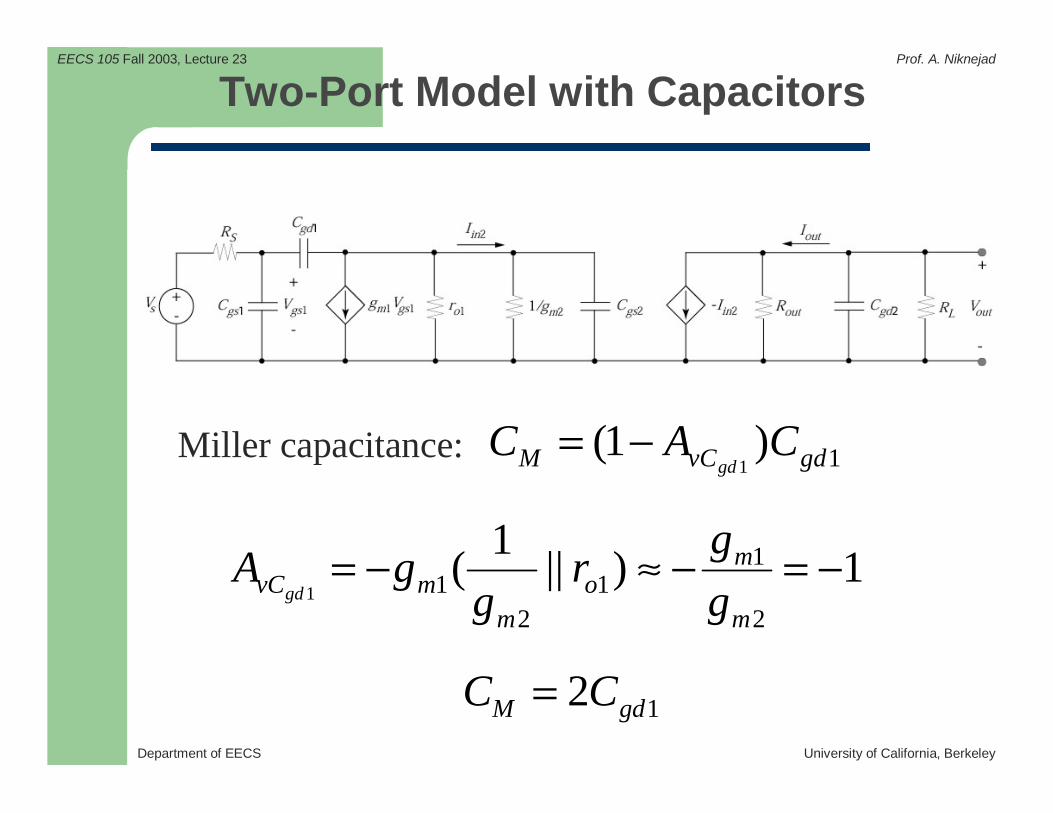
Two-Port Model with Capacitors
Miller capacitance: 1)1(1 gdvCM CAC
gd−=
1
11 1
2 2
1( || ) 1
gd
mvC m o
m m
gA g r
g g= − ≈ − = −
12M gdC C=
Department of EECS University of California, Berkeley
EECS 105 Fall 2003, Lecture 23 Prof. A. Niknejad
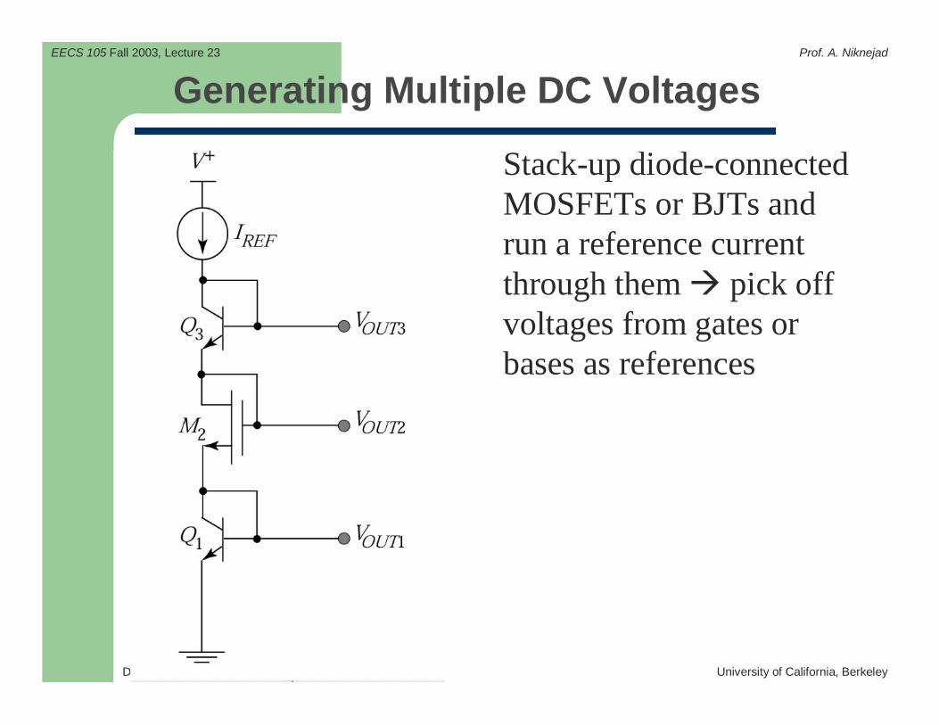
Generating Multiple DC Voltages
Stack-up diode-connected MOSFETs or BJTs and run a reference current through them pick off voltages from gates or bases as references

Department of EECS University of California, Berkeley
EECS 105 Fall 2003, Lecture 23 Prof. A. Niknejad
Multistage Amplifier Design Examples
Start with basic two-stage transconductance amplifier:
Why do this combination?
Department of EECS University of California, Berkeley
EECS 105 Fall 2003, Lecture 23 Prof. A. Niknejad
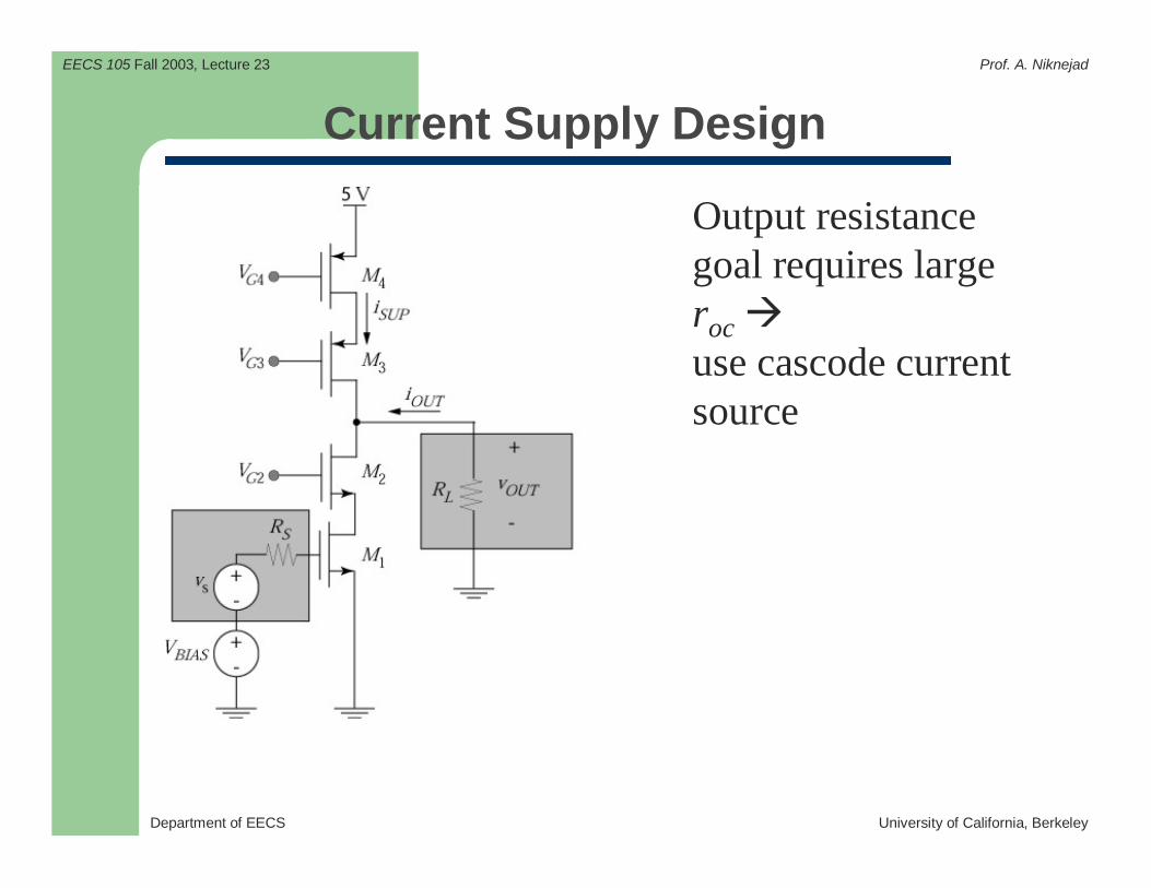
Current Supply Design
Output resistance goal requires large roc
use cascode current source
Department of EECS University of California, Berkeley
EECS 105 Fall 2003, Lecture 23 Prof. A. Niknejad
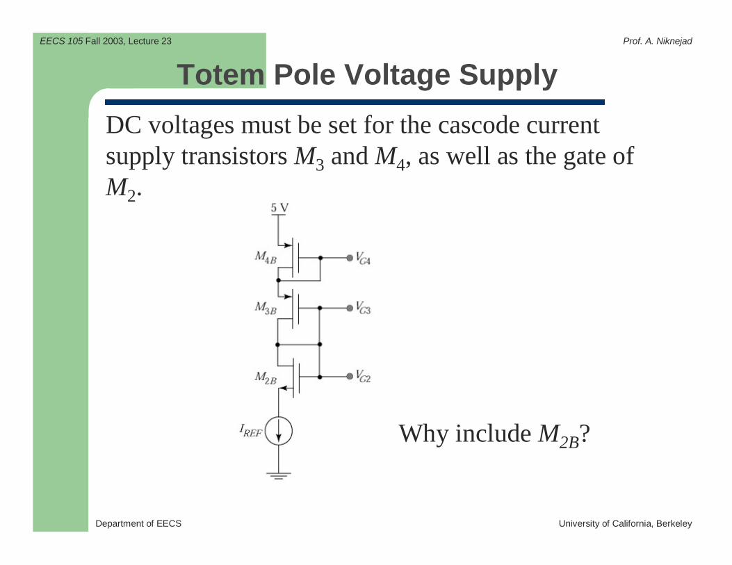
Totem Pole Voltage Supply
DC voltages must be set for the cascode current supply transistors M3 and M4, as well as the gate of M2.
Why include M2B?
Department of EECS University of California, Berkeley
EECS 105 Fall 2003, Lecture 23 Prof. A. Niknejad
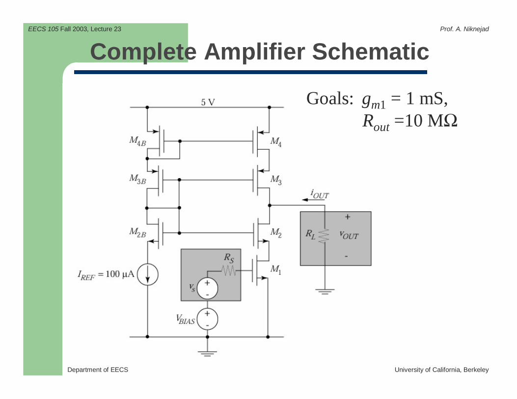
Complete Amplifier Schematic
Goals: gm1 = 1 mS,Rout =10 MΩ
Department of EECS University of California, Berkeley
EECS 105 Fall 2003, Lecture 23 Prof. A. Niknejad
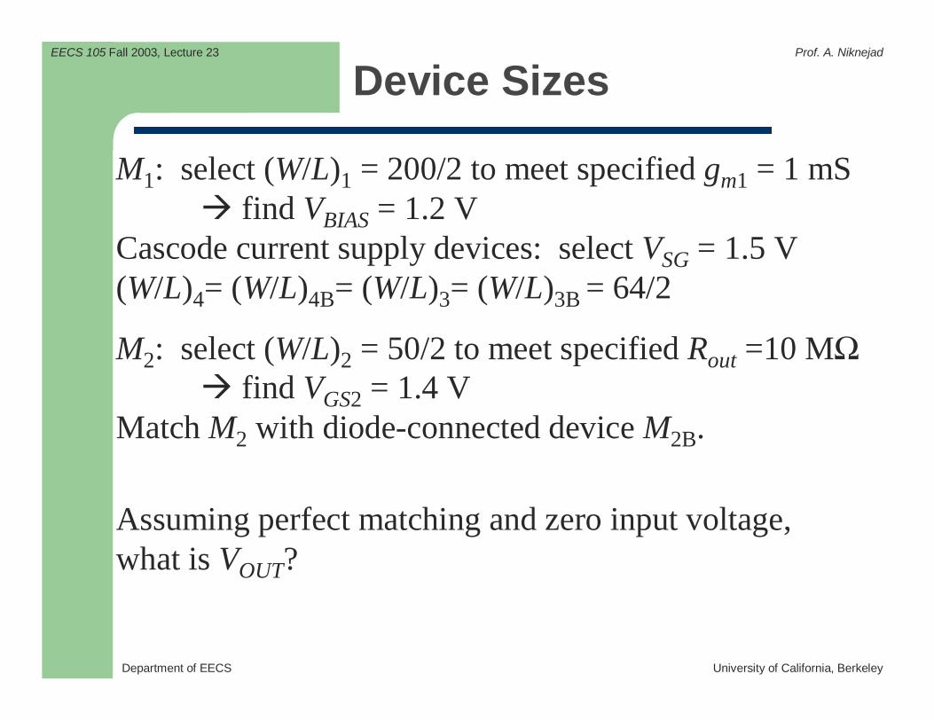
Device Sizes
M1: select (W/L)1 = 200/2 to meet specified gm1 = 1 mS find VBIAS = 1.2 V
Cascode current supply devices: select VSG = 1.5 V(W/L)4= (W/L)4B= (W/L)3= (W/L)3B = 64/2
M2: select (W/L)2 = 50/2 to meet specified Rout =10 MΩ find VGS2 = 1.4 V
Match M2 with diode-connected device M2B.
Assuming perfect matching and zero input voltage,what is VOUT?
Department of EECS University of California, Berkeley
EECS 105 Fall 2003, Lecture 23 Prof. A. Niknejad
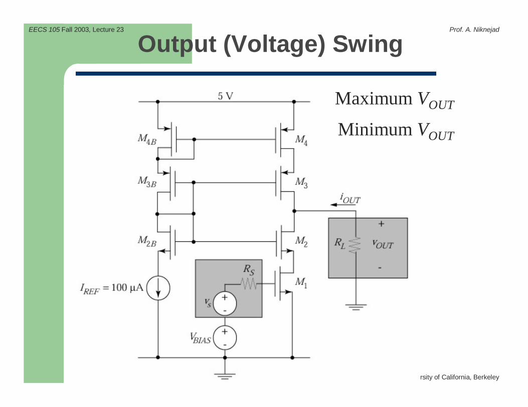
Output (Voltage) Swing
Maximum VOUT
Minimum VOUT

Department of EECS University of California, Berkeley
EECS 105 Fall 2003, Lecture 23 Prof. A. Niknejad
Two-Port ModelFind output resistance Rout
λn = (1/20) V-1, λn = (1/50) V-1 at L = 2 µm ron = (100 µA / 20 V-1)-1 = 200 kΩ, rop = 500 kΩ
( ) ( ) ( )122333222 1||11|| omoSmoSmoocout rgrRgrRgrrR ++=+=
SVV
A
VV
Ig
TnGS
Dm µµ
50014.1
)100(22
2
22 =
−=
−=
SVV
A
VV
Ig
TpSG
Dm µµ
40015.1
)100(2)(2
3
33 =
−=
+−=
Department of EECS University of California, Berkeley
EECS 105 Fall 2003, Lecture 23 Prof. A. Niknejad
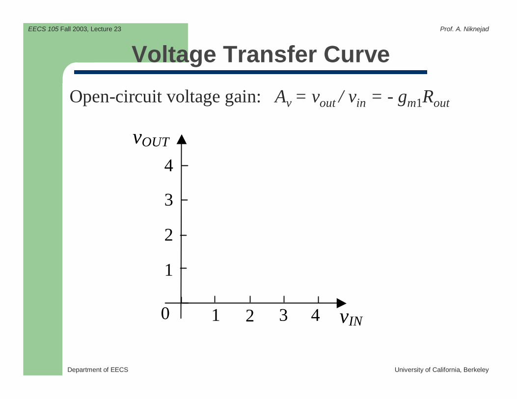
Voltage Transfer Curve
Open-circuit voltage gain: Av = vout / vin = - gm1Rout
vOUT
vIN
3
4
1
2 1 0 3 4
2
Department of EECS University of California, Berkeley
EECS 105 Fall 2003, Lecture 23 Prof. A. Niknejad
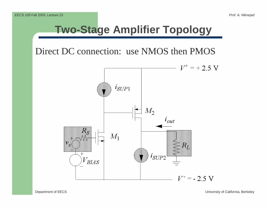
Two-Stage Amplifier Topology
Direct DC connection: use NMOS then PMOS
Department of EECS University of California, Berkeley
EECS 105 Fall 2003, Lecture 23 Prof. A. Niknejad
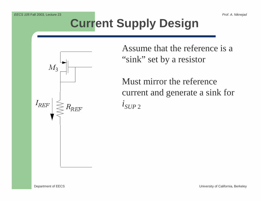
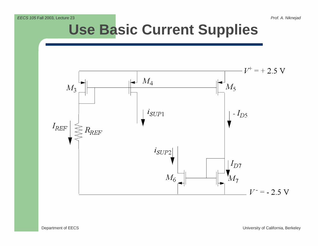
Current Supply Design
Assume that the reference is a “sink” set by a resistor
Must mirror the reference current and generate a sink for iSUP 2
Department of EECS University of California, Berkeley
EECS 105 Fall 2003, Lecture 23 Prof. A. Niknejad
Use Basic Current Supplies
Department of EECS University of California, Berkeley
EECS 105 Fall 2003, Lecture 23 Prof. A. Niknejad
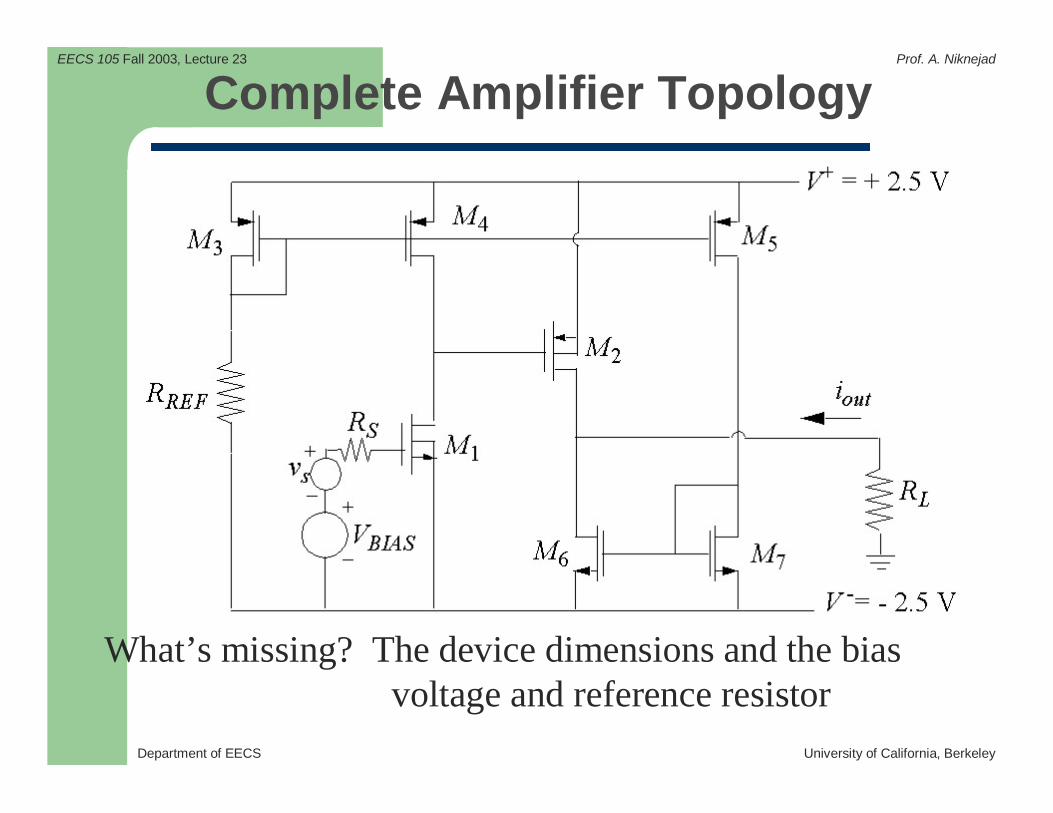
Complete Amplifier Topology
What’s missing? The device dimensions and the biasvoltage and reference resistor