lecture 2, crystal structures crystal structures
TRANSCRIPT

1
Lecture 2, Crystal Structures
1. Crystal structures
2. Crystal geometry
3. X-ray diffraction
4. Crystal defects
• Point defects
• Dislocations
• Planar defects
Crystal Structures
a ceramic (crystalline) and a glass (non-crystalline)
SiO272%
Na2O and CaO 28%
Crystalline structure - the atoms of the material are arranged in a regular and repeating manner over large atomic distances (long-range order)
amorphous materials
nanomaterials

2
Repeating unit cell
Lattice parameters a, b, c, a, b, g
Cubic: a=b=c, a=b=g=90º
Unit cell: is chosen to represent the symmetry of the crystal structure,
•small repeat entity,
•basic structural unit
•building block of crystal strucutre
A parallelepiped
The seven crystal systems
Cubic
Tetragonal
Orthorhombic
Rhombohedral
Hexagonal
Monoclinic
Triclinic
3
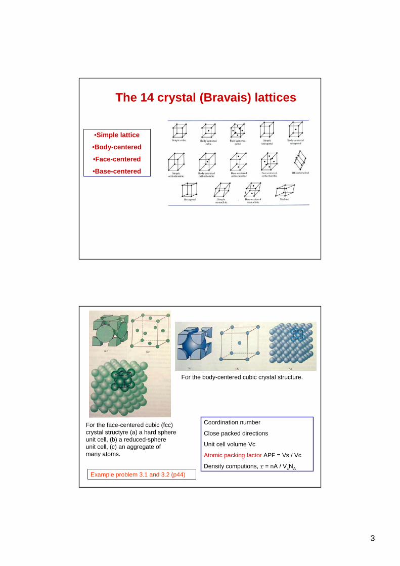
The 14 crystal (Bravais) lattices
•Simple lattice
•Body-centered
•Face-centered
•Base-centered
Coordination number
Close packed directions
Unit cell volume Vc
Atomic packing factor APF = Vs / Vc
Density computions, r = nA / VcNA
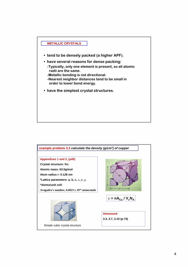
For the face-centered cubic (fcc) crystal structyre (a) a hard sphere unit cell, (b) a reduced-sphere unit cell, (c) an aggregate of many atoms.
For the body-centered cubic crystal structure.
Example problem 3.1 and 3.2 (p44)
4
• tend to be densely packed (a higher APF).
• have several reasons for dense packing:-Typically, only one element is present, so all atomic
radii are the same.-Metallic bonding is not directional.-Nearest neighbor distances tend to be small in
order to lower bond energy.
• have the simplest crystal structures.
METALLIC CRYSTALS
example problem 3.3 calculate the density (g/cm3) of copper
Appendixes 1 and 2, (p45)
Crystal structure: fcc
Atomic mass: 63.5g/mol
Atom radius r: 0.128 nm
*Lattice parameters: a, b, c, a, b, g
*Atoms/unit cell:
Avogadro’s number, 0.6023 x 1024 atoms/mole
Homework
3.3, 3.7, 3.10 (p.74)
r = nACu / VcNA
Simple cubic crystal structure
5
6
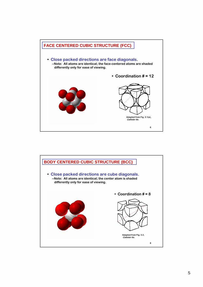
• Coordination # = 12
Adapted from Fig. 3.1(a),Callister 6e.
• Close packed directions are face diagonals.--Note: All atoms are identical; the face-centered atoms are shaded
differently only for ease of viewing.
FACE CENTERED CUBIC STRUCTURE (FCC)
• Coordination # = 8
8
Adapted from Fig. 3.2,Callister 6e.
• Close packed directions are cube diagonals.--Note: All atoms are identical; the center atom is shaded
differently only for ease of viewing.
BODY CENTERED CUBIC STRUCTURE (BCC)
6
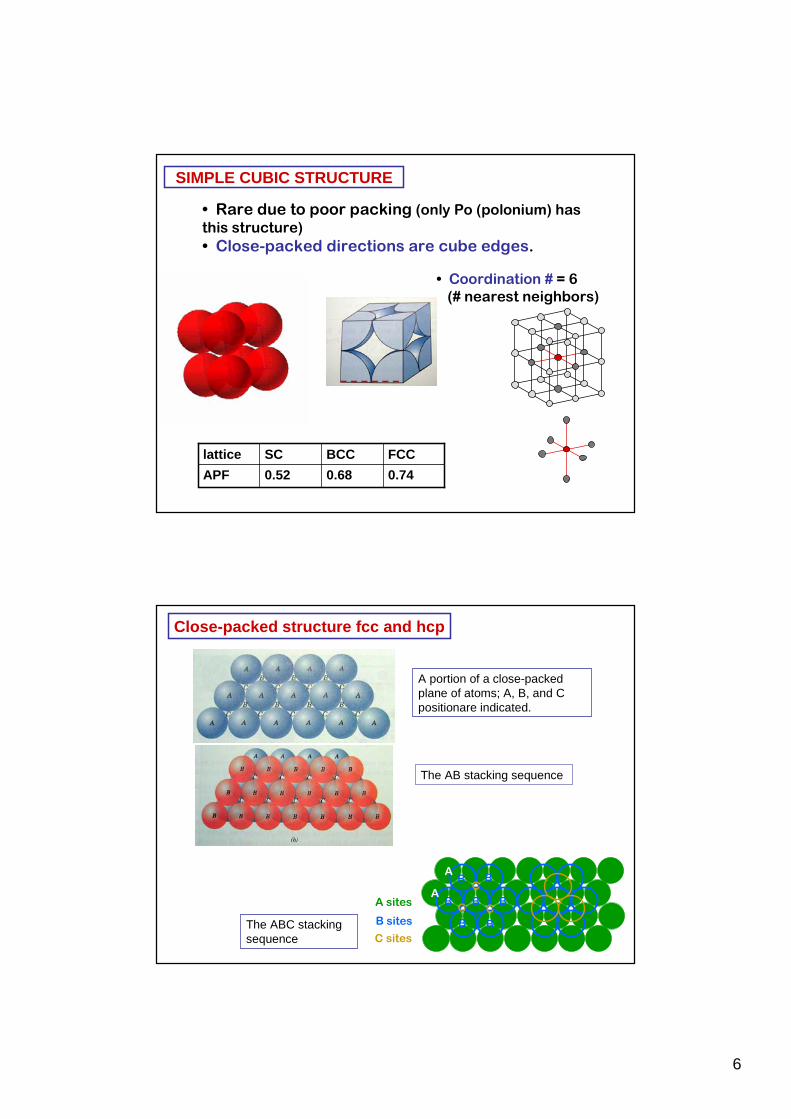
• Rare due to poor packing (only Po (polonium) has this structure)• Close-packed directions are cube edges.
• Coordination # = 6(# nearest neighbors)
SIMPLE CUBIC STRUCTURE
0.740.680.52APF
FCCBCCSClattice
The AB stacking sequence
Close-packed structure fcc and hcp
A sites
B sites
C sitesB B
B
BB
B BC C
CA
A
The ABC stacking sequence
A portion of a close-packed plane of atoms; A, B, and C positionare indicated.

7
(a) A reduced-sphere unit cell, (b) an aggregate of many atoms
Hexagonal close-packed crystal structure
Bottom layer
Middle layer
Top layer
Close-packing stacking for face-centered cubic
8
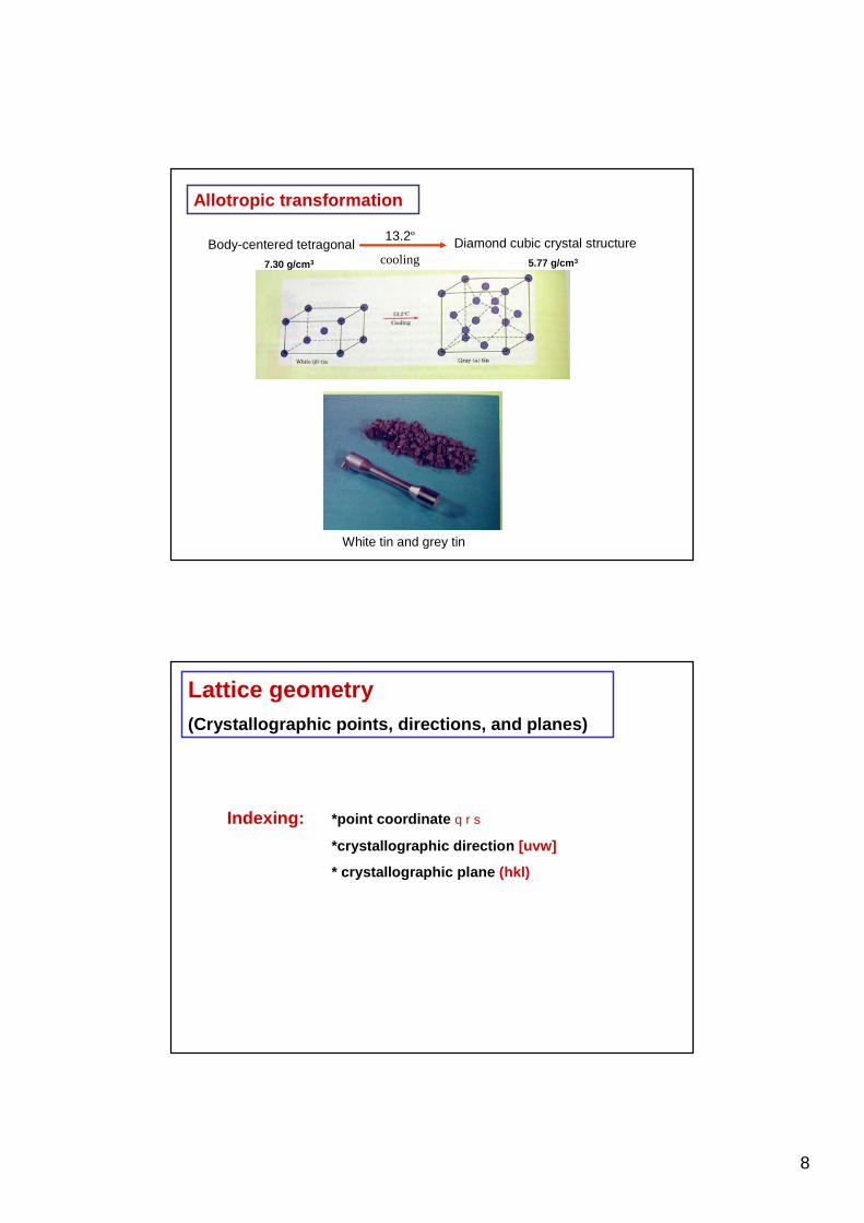
13.2º
cooling
Allotropic transformation
White tin and grey tin
Body-centered tetragonal7.30 g/cm3
Diamond cubic crystal structure5.77 g/cm3
Indexing: *point coordinate q r s
*crystallographic direction [uvw]
* crystallographic plane (hkl)
Lattice geometry(Crystallographic points, directions, and planes)
9
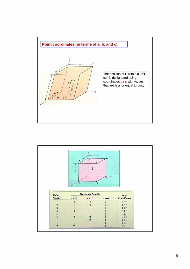
Point coordinates (in terme of a, b, and c)
The position of P within a unit cell is designated using coordinates q r s with values that are less or equal to unity

10
Crystallographic directions [uvw]
1. A vector to be positioned such that it passes through the origin of the coordinate system,
2. To obtain the length of the vector projection on each of the three axes in terms of a, b, and c
3. To reduce them to the smallest integer values
4. The three indices to be enclosed in square brackets, thus [uvw].
Projections
Projections (in terms of a, b, and c)
Reduction
enclosure
Question 3.30 (p76) Sketch within a cubic unit cell the following directions: [101], [ 1 ]; [211]; .......1 1

11
Question 3.31 (p76) Determine the indices for the directions shown in the following cubic unit cell
Crystallographic planes
Intercepts (in terms of lattice parameters)Reciprocals of the numbers, or the inverse
interceptsReductions (multiplied or divided by a commen
factor to reduce them to the smallest integers))
Enclosed within parentheses (hkl)
x y z
1. The crystallographic planes are specified by three Miller indices (hkl).
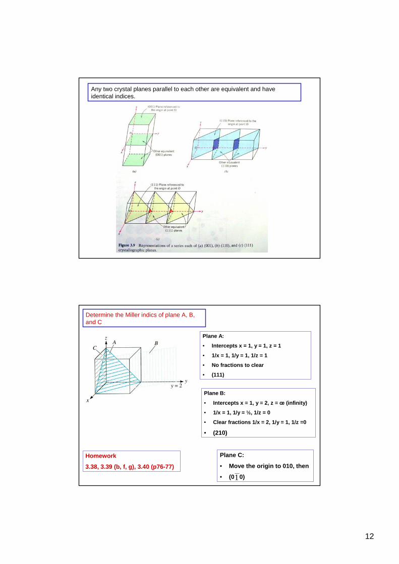
2. Any two crystal planes parallel to each other are equivalent and have identical indices.
3. The plane intercepts or parallels each of the three axes
12
Any two crystal planes parallel to each other are equivalent and have identical indices.
Determine the Miller indics of plane A, B, and C
Plane A:
• Intercepts x = 1, y = 1, z = 1
• 1/x = 1, 1/y = 1, 1/z = 1
• No fractions to clear
• (111)
Plane B:
• Intercepts x = 1, y = 2, z = œ (infinity)
• 1/x = 1, 1/y = ½, 1/z = 0
• Clear fractions 1/x = 2, 1/y = 1, 1/z =0
• (210)
Plane C:
• Move the origin to 010, then
• (0 0)1
Homework
3.38, 3.39 (b, f, g), 3.40 (p76-77)
13
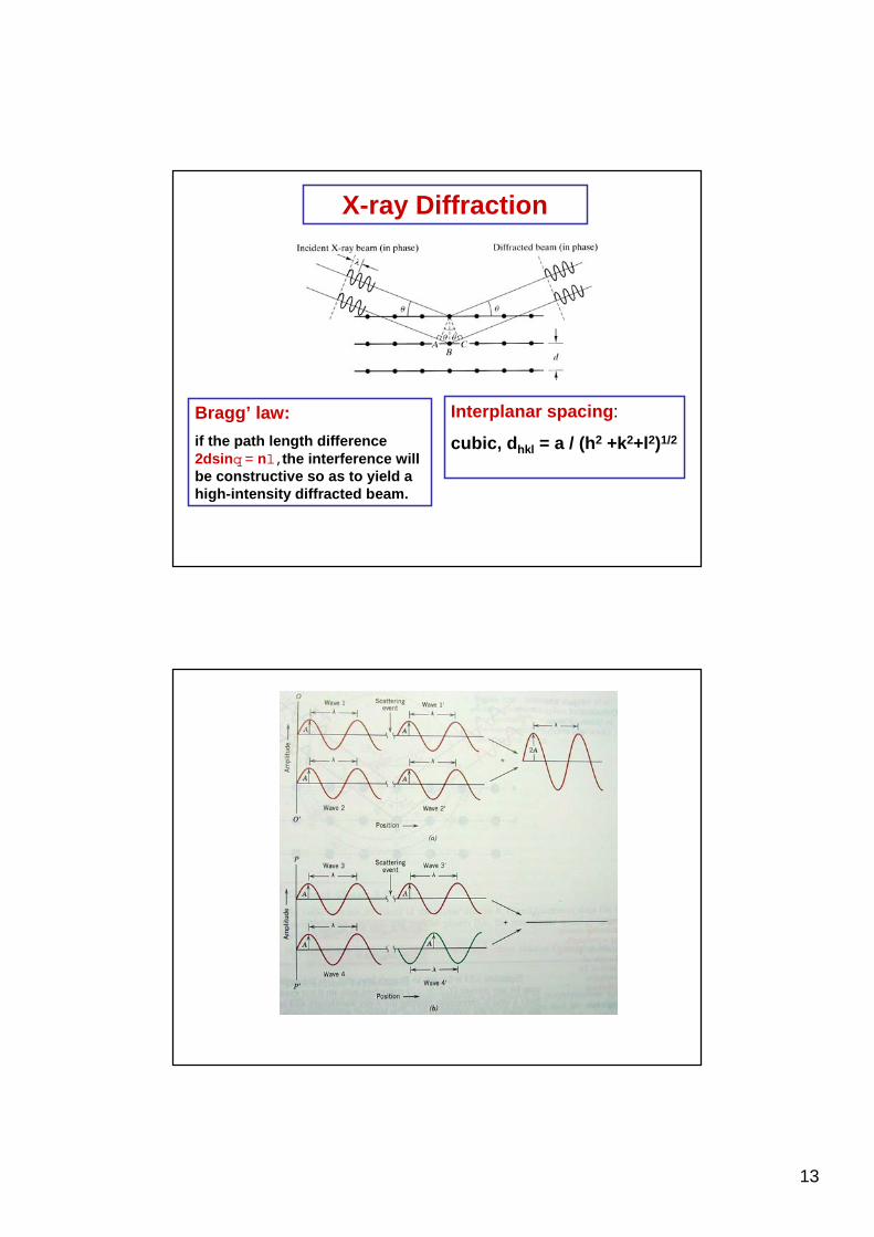
X-ray Diffraction
Interplanar spacing:
cubic, dhkl = a / (h2 +k2+l2)1/2
Bragg’ law:
if the path length difference 2dsinq = nl, the interference will be constructive so as to yield a high-intensity diffracted beam.

14
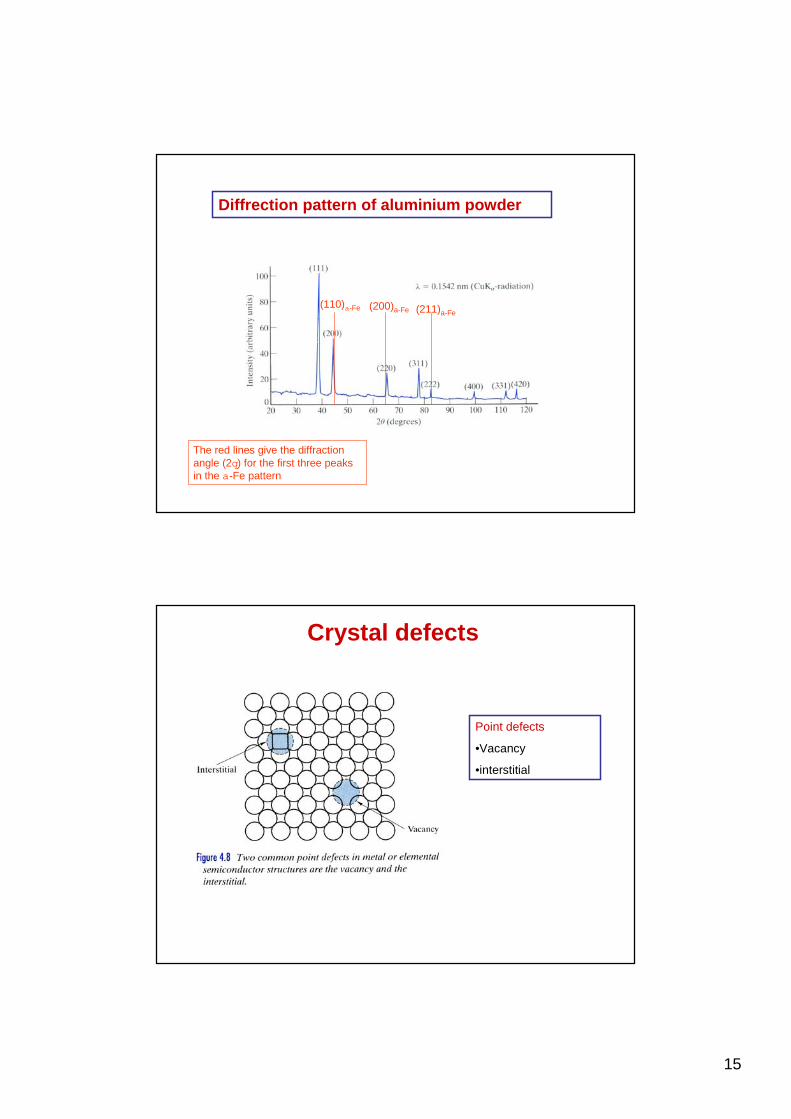
X-ray Diffractometer
Diffrection pattern of aluminium powder
15
Diffrection pattern of aluminium powder
(110)a-Fe (200)a-Fe (211)a-Fe
The red lines give the diffraction angle (2q) for the first three peaks in the a-Fe pattern
Crystal defects
Point defects
•Vacancy
•interstitial

16
3
• Vacancies:-vacant atomic sites in a structure.
Vacancydistortion of planes
• Self-Interstitials:-"extra" atoms positioned between atomic sites.
self-interstitialdistortion
of planes
POINT DEFECTS
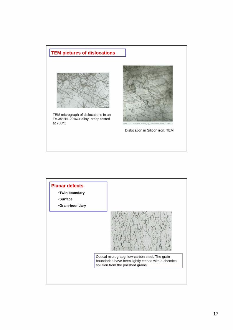
Disloctions•Linear defects
•Associated with mechanical properties
•Synbol represent the edge of an extra half-plane of atom
•Can be seen by using TEM (transmission electron microscopy)
17
Dislocation in Silicon iron. TEM
TEM micrograph of dislocations in an Fe-35%Ni-20%Cr alloy, creep tested at 700ºC
TEM pictures of dislocations
Planar defects•Twin boundary
•Surface
•Grain-boundary
Optical micrograpg, low-carbon steel. The grain boundaries have been lightly etched with a chemical solution from the polished grains.
18
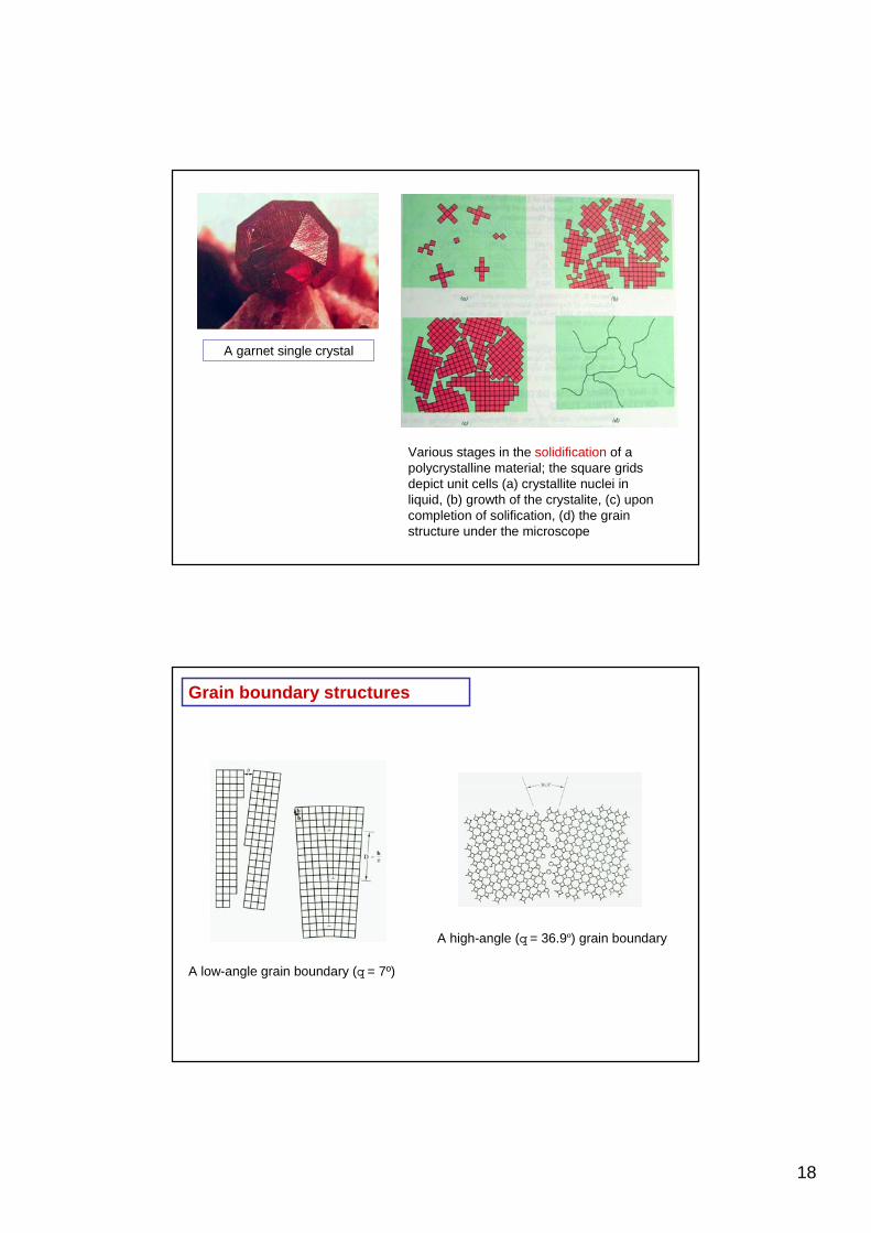
A garnet single crystal
Various stages in the solidification of a polycrystalline material; the square grids depict unit cells (a) crystallite nuclei in liquid, (b) growth of the crystalite, (c) upon completion of solification, (d) the grain structure under the microscope
Grain boundary structures
A high-angle (q = 36.9º) grain boundary
A low-angle grain boundary (q = 7º)
19
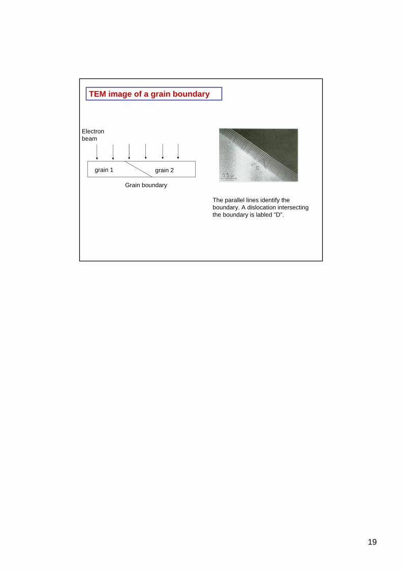
TEM image of a grain boundary
The parallel lines identify the boundary. A dislocation intersecting the boundary is labled ”D”.
grain 1 grain 2
Grain boundary
Electron beam