lecture 13: introduction to thin film characterization...
TRANSCRIPT
Lecture 13:Introduction to Thin Film
Characterization: Surface Analysis (XPS, AES, SIMS, RBS)
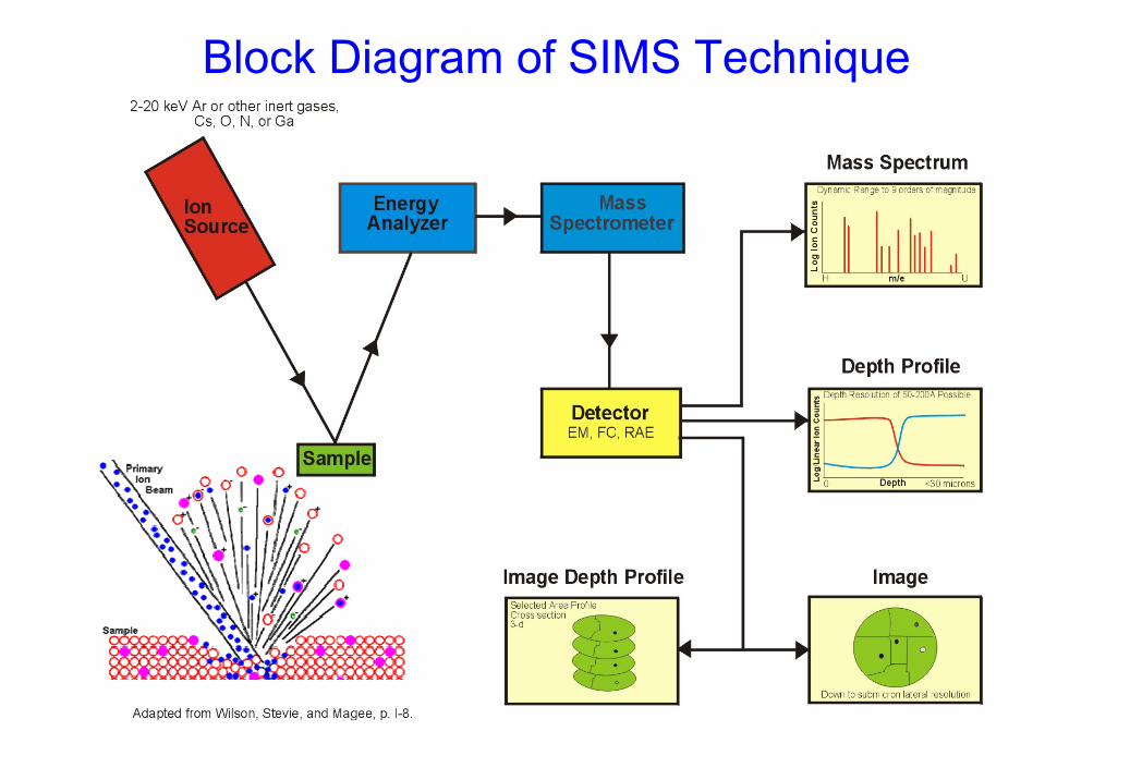
Block Diagram of SIMS Technique

Dynamic SIMS: Magnetic Sector Mass Spectrometer

Effect of Primary Beam on Secondary Ion YieldsEffect of Primary Beam on Secondary Ion Yields
Oxygen bombardmentWhen sputtering with an oxygen beam, the concentration of oxygen increases in the surface layer and metal-oxygen bonds are present in an oxygen-rich zone. When the bonds break during the bombardment-secondary ion emission process, oxygen becomes negatively charged because of its high electron affinityand the metal is left with the positive charge. Elements in yellow analyzed with oxygen bombardment, positivesecondary ions for best sensitivity.Cesium bombardmentWhen sputtering with a cesium beam, cesium is implanted into the sample surface which reduces the workfunction allowing more secondary electrons to be excited over the surface potential barrier. With the increasedavailability of electrons, there is more negative ion formation. Elements in green analyzed with cesium, negativesecondary ions for best sensitivity.
Graphics courtesy of Charles Evans & Associates web sitehttp://www.cea.com

QUANTITATIVE DEPTH PROFILES to study correlation of unintentional hydrogen passivation of acceptors in heavily C-doped GaAs by ambient conditions during cool down following growth by MOCVD
Detects hydrogenLarge dynamic range
Depth Profile Application with HydrogenDepth Profile Application with Hydrogen

Ion Imaging with Dynamic SIMSIon Imaging with Dynamic SIMS

CROSS-SECTIONAL ION IMAGES GENERATED FROM SEQUENTIAL IMAGES IN DEPTH PROFILE
Two Dimensional Imaging with Dynamic SIMSTwo Dimensional Imaging with Dynamic SIMS

Comparison of Static and Dynamic SIMS
TECHNIQUE
STATIC
DYNAMIC
Flux
<1013 ions/cm2
(per experiment)
~1017 ions/cm2
(minimum dose density) Information
Chemical
Elemental
Sensitivity
.01%
<1 ppm
(ppb for some elements) Type of Analysis
Surface Mass Spectrum
Surface Ion Image
Depth Profile Mass Spectrum
Ion Image Image Depth Profile Quantitative Analysis
Sampling Depth (monolayers)
2
10
Spatial Resolution
~0.1 µm
Best: 20 nm (Ga Source) Cameca ims 5f:
Probe Mode: 200 nm Microscope Mode: 1µ
Sample Damage
Minimal
Destructive in analyzed area—
up to 500µ per area

The PHI TRIFT III TOF SIMS is a time-of-flight secondary ion mass spectrometer which employs three hemispherical electrostatic analyzers. It is equipped with Ga and Au analysis ion guns and Cs and O2 sputtering ion guns. The instrument is used for static and dynamic SIMS with high mass resolution up to 15,000 m/∆m. The mass range is 1-5000 amu. The instrument has a cooling stage
Time-of-Flight Secondary Ion Mass Spectrometry

TRIFT Secondary Ion Trajectories
Ga+
Cs+
Pre-SpectrometerBlanker
SED
Detector
ContrastDiaphragm
ESA 1
ESA 2ESA 3
EnergySlitPost-
SpectrometerBlanker
Sam
ple

In+ Linescans of Quantum Dots
µm0 0.5 1.0 1.5 2.0
0
5
10
15
20
µm0 0.5 1.0 1.5
0
5
10
15
µm0 0.5 1.0 1.5 2.0 2.5 3.0 3.5
0
5
10
15
20
25
Cts: 550893; Max: 36; Scale: 1µm
InAs/GaAs Quantum Dots

GaAs/AlGaAs
Al
Ga
Analysis beam: 15kV Ga+
Sputter Beam: 300V O2+ with oxygen flood

Trace Analysis of GaAs
85.85 85.90 85.95 86.00Mass [m/z]
0
5000
10000
15000
20000
Cou
nts
GaOH
71GaNH3
m/∆m = 11,600
Trace analysis of Si Wafer
38.94 38.96 38.98 39.00 39.02 39.04Mass [m/z]
010
110
210
310
410
510
610
Cou
nts
K
C3H3
C2HN
No sputtering to remove organics on surface.Large C3H3 peak does not have a tail to lower mass which would obscure C2HN and K.
No Pre-Sputter to remove organics

Polymer sample
300 350 400 450Mass [m/z]
0100200300400500600
Cou
nts
PEO_2000_900C_P.TDC
373 405331 361317 449 493433 477345 389
500 600 700 800 900Mass [m/z]
0100200300400500600
Cou
nts
PEO_2000_900C_P.TDC
829581 669625653537 741697609565521
1000 1200 1400 1600 1800Mass [m/z]
050
100150200250300
Cou
nts
PEO_2000_900C_P.TDC
150713741270113811831094
1050

Auger Electron SpectroscopyAuger Electron Spectroscopy
Primary beam = 3-20KeV electronsSampling distance = 2 to 4 nmDetection sensitivity =~ 1 atomic %Elements = Li and above Schematic of Auger system with
Cylindrical Mirror Analyzer (CMA)
Auger energy is specific to element
AES is a technique which uses an electronprobe to generate Auger electrons at thesample surface.

Relative Probabilities of RelaxationRelative Probabilities of Relaxationof a K Shell Core Holeof a K Shell Core Hole
5
B Ne P Ca Mn Zn Br Zr
10 15 20 25 30 35 40 Atomic Number
Elemental Symbol
0
0.2
0.4
0.6
0.8
1.0
Pro
babi
lity
Note: The lightNote: The lightelements have aelements have alow cross sectionlow cross sectionfor X-rayfor X-rayemission.emission.
Auger ElectronAuger ElectronEmissionEmission
X-ray PhotonX-ray PhotonEmissionEmission
INCIDENTELECTRON
STEP 2L electron fallsto fill vacancy
K
L1
L2
L3
FERMILEVEL
FREEELECTRONLEVEL
CONDUCTION BAND
VALENCE BAND
1s
2s
2p
STEP 1Ejected electron
STEP 3KLL Auger electronemitted to conserveenergy released instep 2
STEP 3 (alternative)an x-ray is emittedto conserve energyreleased in step 2
THE AUGER PROCESS
The emitted Auger electron is designated the (core hole) (step 2 level) (step 3 level) transition ie. (KLL) transition.
The kinetic energy of the emitted Auger electron is : E(Auger) = E(K) - E(L2) - E(L3).
The energy of the emitted X-ray is : E(X-ray) = E(K) - E(L2).
-or-
Ref: Charles Evans & Assoc. web page tutorial by Ron Flleming http://www.cea.com
INCIDENTELECTRON
EJECTED CORE ELECTRON
EJECTED AUGER ELECTRON

AES Imaging and ProfilingAES Imaging and Profiling
SPUTTER TIME (MIN.)
PEA
K-TO
-PE
AK
Fracture surface of Carbon fibers in BN matrix - analysis area outlined in black
Depth profile on fiber to determine point of fracture. Variations in fracture surfaceinterface for different sample treatments will be reflected in depth profile.
From research by C. Cofer/J. Economy, Materials Science Dept.
50 100 150 200 250 300 350 400 450 500 550-1
-0.8
-0.6
-0.4
-0.2
0
0.2
0.4
0.6
0.8
1x 10⁴
Kinetic Energy (eV)
c/s
COFER73.SPE
Si
BAr
C O
N
Survey on Fiber surface at 1 min. in profile
Electron Beam in combination withan SED detector allows for imagingof the sample to select the area for analysis.

0 200 400 600
O
C
Cr
Cr
VV
Ti
Ti
V VV
Cr
Cr
Ti
Cr
TiTiN
KL 2,
3L2,
3
Sc M
1M4M
4
Sc M
2,3M
4M4
Cou
nts
(arb
. uni
ts) N K
L 2,3L
2,3
Sc L
3M2,
3M2,
3
Sc L
3M2,
3M4,
5
Sc L
3M4,
5M4,
5
3 keV spectra - as deposited
Kinetic energy (eV)0 200 400 600
Cr Cr Cr Cr
Cr
VV VVV
TiTi
TiTiTi
Sc M
1M4M
4
Sc M
2,3M
4M4
Cou
nts
(arb
. uni
ts)
N K
L 2,3L
2,3
Sc L
3M2,
3M2,
3Sc
L3M
2,3M
4,5
Sc L
3M4,
5M4,
53 keV spectra - as deposited
Kinetic energy (eV)
N(E
)
dN(E
)/dE
E,E,
Auger Electron Spectroscopy First-Row Transition Metal Nitrides: ScN, TiN, VN, and CrN
raw spectra differentiated spectra

AES analysis:
Electron Beam:Voltage: 3, 5, 10 or 20 keVCurrent: 210 nARaster: 0.2 mm x 0.2 mm
Analyzer:Resolution: 0.25 %Step size:0.2 eV/step
Ion Beam: 3 keV Ar+, 0.30 mA/cm2
XPS and UPS analysis:
X-ray source:Al mono 500 W, 15 kVMg Kα 400W, 15 kV
UV source:He I 0.520 kV, 55 mAHe II 0.580 kV, 56 mA
Spot size:1 mm selected area aperture
Analyzer resolution:XPS Survey: 178.95 eV pass energy (2.8 eV resolution), 1 eV/stepElemental regions: 17.95 eV pass energy (0.28 eV resolution), 0.05 eV/stepUPS valence band: 8.95 eV pass energy (0.13 eV resolution), 0.05 eV/step
Emission angle:XPS: 45°UPS: 90°
Ion Beam: 3 keV Ar+, 4.3 µA/cm2

X-ray Photoelectron SpectroscopySmall Area Detection
XX--ray Beamray Beam
XX--ray penetration ray penetration depth ~1depth ~1µµm.m.Electrons can be Electrons can be excited in this excited in this entire volume.entire volume.
XX--ray excitation area ~1x1 cmray excitation area ~1x1 cm22. Electrons . Electrons are emitted from this entire areaare emitted from this entire area
Electrons are extracted Electrons are extracted only from a narrow solid only from a narrow solid angle.angle.
1 mm1 mm22
10 nm10 nm

Photoelectron and Auger Electron Emission
Conduction BandConduction Band
Valence BandValence Band
Fermi LevelFermi Level
Incident XIncident X--rayray
1s1s
2s2s
2p2p
Ejected PhotoelectronEjected Photoelectron
Conduction BandConduction Band
Valence BandValence Band
L2,L3L2,L3
L1L1
KK
Free Electron LevelFree Electron Level
Emitted Auger ElectronEmitted Auger Electron

X-ray Photoelectron Spectrometer
5 4 . 7
XX--rayraySourceSource
ElectronElectronOpticsOptics
Hemispherical Energy AnalyzerHemispherical Energy Analyzer
Position Position Sensitive Sensitive Detector Detector (PSD)(PSD)
Magnetic ShieldShieldOuter SphereOuter Sphere
Inner SphereInner Sphere
SampleSample
Computer Computer SystemSystem

Elemental Shifts
Binding Energy (eV)
Element 2p3/2 3p ∆
Fe 707 53 654
Co 778 60 718
Ni 853 67 786
Cu 933 75 858
Zn 1022 89 933
Electron-nucleus attraction helps us identify theelements

Chemical Shifts
FunctionalGroup
Binding Energy(eV)
hydrocarbon C-H, C -C 285.0
amine C-N 286.0
alcohol, ether C-O-H, C -O-C 286.5
Cl bound to C C-Cl 286.5
F bound to C C-F 287.8
carbonyl C=O 288.0

1200 1000 800 600 400 200 0
CrN
VN
TiN
ScN
Cou
nts
(arb
. uni
ts)
Binding energy (eV)
Metal and N Auger Lines
N1s
N1s
N1s
N1s
Sc2p
Sc2s
Ti2p
V2p
Cr2p
Ti2s
V2s
Cr2s
Sc3pSc3s
Ti3s
V3s
Cr3s
Ti3p
V3p
Cr3p
X-ray Photoelectron SpectroscopyFirst-Row Transition Metal Nitrides: ScN, TiN, VN, and CrN

Analysis of Materials for Solar Energy Collection by XPS Depth Profiling-
The amorphous-SiC/SnO2 InterfaceThe profile indicates a reduction of the SnOThe profile indicates a reduction of the SnO22occurred at the interface during deposition. occurred at the interface during deposition. Such a reduction would effect the collectorSuch a reduction would effect the collector’’s s efficiency.efficiency.
PhotoPhoto--voltaic Collectorvoltaic Collector
Conductive OxideConductive Oxide-- SnOSnO22
pp--type atype a--SiCSiC
aa--SiSi
Solar EnergySolar Energy
SnOSnO22
SnSn
Depth500 496 492 488 484 480
Binding Energy, eV
Data courtesy A. Nurrudin and J. Abelson, University of Illinois

2 MeV Van de Graaff accelerator
4 MeV Tandetron accelerator
Rutherford backscattering spectrometry

0 50 100 150 2000.0
0.2
0.4
0.6
0.8
1.0
θ = 150o
He4
Kin
emat
ic fa
ctor
: K
Target mass (amu)
22 22 sin cost i i
i t
MMMKM M
θ θ +−= +
24( , ) sin ( ) 2( )
4 2 t
i t iR
Z Z ME MEθσ θ − ∝ −
Rutherford backscattering spectrometry, cont.
Elastic scattering
E1 = KEo
Rutherford scattering cross section
Coulomb interaction between the nuclei:exact expression

Rutherford backscattering spectrometry, cont.
atoms/cm2
Figure after W.-K. Chu, J. W. Mayer, and M.-A. Nicolet, Backscattering Spectrometry (Academic Press, New York, 1978).

Au
In
TiAlO
C10 ML 100 ML
RBS – simulated spectrahypothetical alloy Au0.2In0.2Ti0.2Al0.2O0.2/C
Au
In
TiAlOC
Au
In
TiAlOC
Au
In
TiAlOC
Au
In
Ti
AlO
C Au
InTi
Al
O
1000 ML
2000 ML 4000 ML 10000 ML
Element (Z,M): O(8,16), Al(13,27), Ti(22,48), In(49,115), Au(79,197)

RBS: Oxidation behavior
TiN/SiO2TaN/SiO2
Ta = 600 °C for 12 min in atmosphere
As-deposited
Annealed

I. Petrov, P. Losbichler, J. E. Greene, W.-D. Münz, T. Hurkmans, and T. Trinh, Ion-Assisted Growth of Ti1-xAlxN/Ti1-
yNbyN Multilayers by Combined Cathodic-Arc/Magnetron-Sputter Deposition, Thin Solid Films, 302 179 (1997)
Example: average composition Ti0.27Al0.20Nb0.02N0.51

Comparison of Detection Limits by TechniqueComparison of Detection Limits by Technique