lds-mid design design guide - 3d-mid-company | …€¦ · 3.1 overview of lds mid design rules ......
TRANSCRIPT

LDS-MID Design GuideTechnical Information
Order Code: 10028429

LDS-MID Design Guide
Technical Information
Version 2.1
English

LDS-MID Design Guide
2 2010 LPKF AG
LDS-MID Design Guide
2010 LPKF AG 3
Document information
Division Usage Author Distribution Status date Status MPV External W. John Customer, Service 2010-07-16 draft MPV External W. John Customer, Service 2010-10-01 Released MPV External W. John Customer, Service 2010-11-10 Released
Document history Version Date Editor Comment 2.0 2010-07-16 KCHR Draft German version created 2.0 2010-08-03 KCHR Corrections done 2.0 2010-0827 TW Translation 2.0 2010-10-01 KCHR Released version created 2.1 2010-10-20 TW Changes applied 2.1 2010-11-10 KCHR Released version created

LDS-MID Design Guide
4 2010 LPKF AG

LDS-MID Design Guide Content
2010 LPKF AG TI V2.1/Nov-10 5
Content
1 Introduction .......................................................................................... 7
2 Materials ............................................................................................... 9
2.1 Material types ............................................................................................................ 9 2.2 Suppliers ................................................................................................................... 9 2.3 Material selection criteria ........................................................................................ 10
3 General design rules and recommendations .................................. 11
3.1 Overview of LDS MID design rules ......................................................................... 11 3.2 LDS-MID design rules ............................................................................................. 12
4 Injection moulding ............................................................................. 27
4.1 Tool design ............................................................................................................. 27 4.1.1 Material ......................................................................................................... 27 4.1.2 Tool surface .................................................................................................. 27 4.1.3 Design rules for sprue and gate ................................................................... 27
4.2 Injection moulding process ..................................................................................... 28 4.3 Handling, packaging, and storage .......................................................................... 28
4.3.1 Handling ........................................................................................................ 28 4.3.2 Packaging and storage ................................................................................. 28
5 Laser Processing ............................................................................... 29
5.1 Data Preparation ..................................................................................................... 29 5.1.1 Avoid short fill vectors ................................................................................... 29 5.1.2 Laser parameters ......................................................................................... 30 5.1.3 Other process parameters ............................................................................ 30
5.2 Laser Processing .................................................................................................... 31 5.2.1 Fixture ........................................................................................................... 31 5.2.2 Positioning .................................................................................................... 31
5.3 Handling, packaging, and storage .......................................................................... 31 5.3.1 Handling ........................................................................................................ 31 5.3.2 Packaging ..................................................................................................... 31 5.3.3 Storage ......................................................................................................... 32
6 Metallisation ....................................................................................... 33
6.1 Component retainers .............................................................................................. 33 6.2 Cleaning LDS MIDs ................................................................................................ 33 6.3 Electrolytes for metallisation ................................................................................... 34 6.4 Metallisation Process .............................................................................................. 35
6.4.1 Processing order .......................................................................................... 35 6.4.2 Metallisation processes/process steps ......................................................... 35
6.5 Thermal conditioning............................................................................................... 36 6.6 Handling .................................................................................................................. 36
7 Quality assurance .............................................................................. 37
Content LDS-MID Design Guide
6 TI V2.1/Nov-10 2010 LPKF AG
8 Appendix ............................................................................................ 39
8.1 Table of figures ....................................................................................................... 39 8.2 List of tables ............................................................................................................ 39 8.3 List of abbreviations ................................................................................................ 40 8.4 Conversion tables ................................................................................................... 41
ddd

LDS-MID Design Guide Introduction
2010 LPKF AG TI V2.1/Nov-10 7
1
Pos: 1 /ED_Technische_Dokumentation/7_Design_Guides/MID_Systeme/LDS_Design_Guide/Kapitel_1_Einleitung/1_Einleitung @ 0\mod_1287993377025_2058.docx @ 11280 @ 1
1 Introduction Developing MID components (moulded interconnect devices) is a complex procedure no matter which process or technology is used. This guide helps especially the developer of MIDs that are based on the LPKF laser direct structuring process (LPKF-LDS® process) in the interdisciplinary development process. To avoid errors or designs unsuitable for production, a very close cooperation between all participants in the individual processes is required already in the early stages of the project. This applies not only to the LDS process steps injection moulding, laser structuring, and metallisation that are discussed in more detail in this document, but extends to the area of mounting and bonding of electronic components in case of populated MIDs.

Introduction LDS-MID Design Guide
8 TI V2.1/Nov-10 2010 LPKF AG
1

LDS-MID Design Guide Materials
2010 LPKF AG TI V2.1/Nov-10 9
2
Pos: 2 /ED_Technische_Dokumentation/7_Design_Guides/MID_Systeme/LDS_Design_Guide/Kapitel_2_Werkstoffe/2_1_Werkstoffklassen @ 0\mod_1287993391415_2058.docx @ 11285 @ 12
2 Materials Nowadays, a whole range of thermoplastic materials is available for manufacturing LDS MID components.
2.1 Material types
The following materials can be used in the LDS process:
Table 1: Materials Type Material LCP liquid crystal polymer
PA 6/6T polyamide
PBT polybutylene terephthalate
PBT/PET polybutylene terephthalate/polyethylene terephthalate blend
PPA polyphthalamide
PC polycarbonate
PC/ABS polycarbonate + ABS blend
Pos: 3 /ED_Technische_Dokumentation/7_Design_Guides/MID_Systeme/LDS_Design_Guide/Kapitel_2_Werkstoffe/2_2_Lieferanten @ 0\mod_1287993392603_2058.docx @ 11290 @ 2
2.2 Suppliers
LPKF has tested and approved materials for the LDS process from various producers. The following material types are available from the listed producers:
Table 2: Suppliers
Producer Type
BASF AG PA 6/6T
PBT
LANXESS PBT
PET/PBT
TICONA GmbH LCP
RTP Co. PC/ABS
PC
LCP
PPA
DSM Engineering Plastics B.V. PC/ABS
Mitsubishi Engineering-Plastics Corporation
PC
EVONIK INDUSTRIES PBT
WAH HONG Industrial Corp. PC/ABS
Materials LDS-MID Design Guide
10 TI V2.1/Nov-10 2010 LPKF AG
2
Table 2: S li
Producer Type
SABIC Innovative Plastics PC/ABS
PPA
Note
A detailed list of the approved materials can be downloaded from the LPKF website at http://www.lpkf.com/lds-plastics.
Pos: 4 /ED_Technische_Dokumentation/7_Design_Guides/MID_Systeme/LDS_Design_Guide/Kapitel_2_Werkstoffe/2_3_Kriterien der Materialauswahl @ 0\mod_1287993393853_2058.docx @ 11295 @ 2
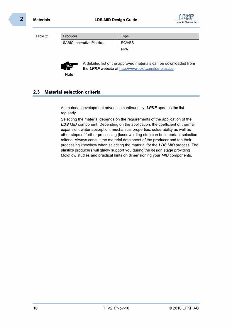
2.3 Material selection criteria
As material development advances continuously, LPKF updates the list regularly. Selecting the material depends on the requirements of the application of the LDS MID component. Depending on the application, the coefficient of thermal expansion, water absorption, mechanical properties, solderability as well as other steps of further processing (laser welding etc.) can be important selection criteria. Always consult the material data sheet of the producer and tap their processing knowhow when selecting the material for the LDS MID process. The plastics producers will gladly support you during the design stage providing Moldflow studies and practical hints on dimensioning your MID components.

LDS-MID Design Guide Design rules
2010 LPKF AG TI V2.1/Nov-10 11
3
Pos: 5 /ED_Technische_Dokumentation/7_Design_Guides/MID_Systeme/LDS_Design_Guide/Kapitel_3_Designregeln/3_1_Überblick @ 0\mod_1287993417571_2058.docx @ 11300 @ 122
3 Design rules The following design rules (DR_xxx_LDS_MID_) help you to achieve optimum results when designing MID components.
3.1 Overview of LDS MID design rules
The following table shows for which process and for which material each design rule applies.
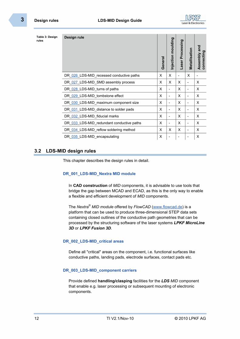
Table 3: Design rules
Design rule
Gen
eral
Inje
ctio
n m
ould
ing
Lase
r Pro
cess
ing
Met
allis
atio
n
Ass
embl
y an
d co
nnec
ting
DR_001_LDS-MID_Nextra MID module X X - - X
DR_002_LDS-MID_critical areas X - - - X
DR_003_LDS-MID_component carriers X X X X X
DR_004_LDS-MID_fiducial marks X - X - X
DR_005_LDS-MID_avoid gate at critical area - X - - -
DR_006_LDS-MID_hot-runner systems - X - X -
DR_007_LDS-MID_weld lines - X X - X
DR_008_LDS-MID_positioning ejector pins - X X - X
DR_009_LDS-MID_material shrinkage - X - - X
DR_010_LDS-MID_coefficient of thermal expansion - X - - X
DR_011_LDS-MID_laser processing time - - X - -
DR_012_LDS-MID_scan field volume X - X - -
DR_013_LDS-MID_width and spacing of conductive paths
X - X X X
DR_014_LDS-MID_datamatrix or barcode X - X X X
DR_015_LDS-MID_thickness of copper layer X X - X X
DR_016_LDS-MID_bond connections X - X X X
DR_017_LDS-MID_plated vias X X X - X
DR_018_LDS-MID_conductive-path passages X X X - -
DR_019_LDS-MID_mechanical vias X X X - X
DR_020_LDS-MID_detachable connection X X X - X
DR_021_LDS-MID_edge radius - - X X -
DR_022_LDS-MID_positioning conductive tracks - - X X X
DR_023_LDS-MID_angle of incidence of laser beam X - X X -
DR_024_LDS-MID_ventilation X X - X -
DR_025_LDS-MID_fastening the plastic components X X - X -
Design rules LDS-MID Design Guide
12 TI V2.1/Nov-10 2010 LPKF AG
3
Table 3: Design rules
Design rule
Gen
eral
Inje
ctio
n m
ould
ing
Lase
r Pro
cess
ing
Met
allis
atio
n
Ass
embl
y an
d co
nnec
ting
DR_026_LDS-MID_recessed conductive paths X X - X -
DR_027_LDS-MID_SMD assembly process X X X - X
DR_028_LDS-MID_turns of paths X - X - X
DR_029_LDS-MID_tombstone effect X - X - X
DR_030_LDS-MID_maximum component size X - X - X
DR_031_LDS-MID_distance to solder pads X - X - X
DR_032_LDS-MID_fiducial marks X - X - X
DR_033_LDS-MID_redundant conductive paths X - X - X
DR_034_LDS-MID_reflow soldering method X X X - X
DR_035_LDS-MID_encapsulating X - - - X
3.2 LDS-MID design rules
This chapter describes the design rules in detail. DR_001_LDS-MID_Nextra MID module
In CAD construction of MID components, it is advisable to use tools that bridge the gap between MCAD and ECAD, as this is the only way to enable a flexible and efficient development of MID components. The Nextra® MID module offered by FlowCAD (www.flowcad.de) is a platform that can be used to produce three-dimensional STEP data sets containing closed outlines of the conductive path geometries that can be processed by the structuring software of the laser systems LPKF MicroLine 3D or LPKF Fusion 3D.
DR_002_LDS-MID_critical areas
Define all "critical" areas on the component, i.e. functional surfaces like conductive paths, landing pads, electrode surfaces, contact pads etc.
DR_003_LDS-MID_component carriers
Provide defined handling/clasping facilities for the LDS MID component that enable e.g. laser processing or subsequent mounting of electronic components.
LDS-MID Design Guide Design rules
2010 LPKF AG TI V2.1/Nov-10 13
3
DR_004_LDS-MID_fiducial marks
Use alignment or registration marks. The registration marks are required for laser processing or for vision systems in the subsequent mounting of electronic components.
DR_005_LDS-MID_avoid gate at critical area
Avoid positioning gates at critical areas when designing the tool.
DR_006_LDS-MID_hot-runner systems
If feasible and the costs are justifiable, choose a hot-runner system over film-gate or direct-gate systems to avoid extraneous metallisations at the break or shear edges that are produced when removing the sprues.
DR_007_LDS-MID_weld lines
Avoid weld lines on critical surfaces. The conductive pattern should not be placed over the weld lines, because this can have critical effects on the conductive paths especially under mechanical stress or temperature variation stress. Pay special attention to conductive patterns and weld lines when employing LCP-type MID materials.
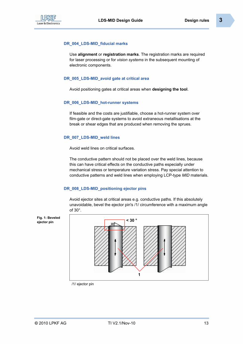
DR_008_LDS-MID_positioning ejector pins
Avoid ejector sites at critical areas e.g. conductive paths. If this absolutely unavoidable, bevel the ejector pin's /1/ circumference with a maximum angle of 30°.
Fig. 1: Beveled ejector pin
/1/ ejector pin
1
< 30 °

Design rules LDS-MID Design Guide
14 TI V2.1/Nov-10 2010 LPKF AG
3
DR_009_LDS-MID_material shrinkage
Pay attention to shrinkage of the component during processing and optimise the injection moulding parameters to minimise shrinkage. Ensure that jetting is avoided when the material is injected into the mould as this leads to undesirable anisotropies when processing the MID components in thermal processes such as soldering. Using a moldflow simulation can be of good service before producing the final mould.
DR_010_LDS-MID_coefficient of thermal expansion
Pay attention to possible anisotropic material characteristics such as the coefficient of thermal expansion (CTE).
DR_011_LDS-MID_laser processing time
When designing the LDS MID component, keep in mind that a low count of clamping steps or processing positions reduces laser processing time and thus enables economic production.
DR_012_LDS-MID_scan field volume
Observe the maximum possible scan field volume (truncated cone with a base diameter of 160 mm, a height of 24 mm, and an angle of 77.4° between the base and the lateral surface in the LPKF MicroLine-3D 160i).
Fig. 2: Scan field volume
/1/ height = 24 mm /3/ angle towards the vertical Z-axis = 12.6° max
/2/ diameter = 160 mm
1
2
3

LDS-MID Design Guide Design rules
2010 LPKF AG TI V2.1/Nov-10 15
3
DR_013_LDS-MID_width and spacing of conductive paths
Observe the minimum width and spacing of conductive paths:
recommended conductive path width 150 μm
recommended conductive path spacing 200 μm
Consult all parties involved in the process (laser processing, metallisation, and assembly) if you wish to use lower values (such as 100 μm width and spacing of conductive paths). When considering the dimensions of conductive paths dependent on the application of the MID assembly, observe that the conductivity of solely chemically deposited copper layers is only approx. 60% of that of solid copper. As the dimension "height of the conductive path" is limited, sufficient current rating can only be achieved by adequate width of the conductive path. The following figure provides an indication for the current rating of chemically deposited conductive copper paths depending on width and thickness with a permissible heating by 40 Kelvin:
Fig. 3: Dimensions of conductive paths
I [A] = current in amperes I-I [mm] = width of conductive path in mm
DR_014_LDS-MID_datamatrix or barcode
The structuring software for the LDS® process provides an option in the process step "laser structuring" for tracking the MID components. For this option, the conductive paths and a serial data matrix code or barcode have to be activated at the same time. The subsequent metallization guarantees good legibility.

Design rules LDS-MID Design Guide
16 TI V2.1/Nov-10 2010 LPKF AG
3
DR_015_LDS-MID_thickness of copper layer
For economic reasons, we recommend to limit the thickness of the chemical copper plating that follows laser structuring to 8 μm for LDS MID components that cannot or are not intended to be galvanically reinforced. For general electronics applications or solder mounting, we recommend electroless nickel/phosphorus or gold plating. Other finish layers such as chemically deposited tin or silver or organic protective passivations can be employed and have to be consulted with the metallisation service provider. If a sufficient layer thickness, e.g. for a required higher current rating, cannot be achieved or is not economically sensible using chemical deposition, the chemical copper plating can be subsequently reinforced by galvanic copper plating. This requires of the layout design that all conductive paths have to be joined at a common contact area. This can be e.g. a surface area on the component that is separated mechanically after metallisation, thus disconnecting the electrical connections of all conductive structures.
DR_016_LDS-MID_bond connections
Applications of "chip on MID" attract more and more interest where the electrical connections between the substrate and the chip that is glued directly onto the substrate have to be made by bonding. There are two general bonding technologies:
1. ultrasonic wedge-wedge bonding using Al/Si wire and
2. thermosonic ball-wedge bonding using Au wire
The following two prerequisites have to be met to successfully bond LDS MID components:
1. A smooth-as-possible bonding surface on the substrate with only rare nodules and an Rz value of 10 μm max. This requires great care when selecting the laser parameters but also when selecting the bath chemicals and in process control of the metallisation.
2. Selecting the correct finish surface for successfully creating bond connections.
Due to the inherent surface roughening of the LDS® process, only ultrasonic wedge-wedge bonds using Al wire have been publicised up to now. Approaches that enable LDS MID components for thermosonic ball-wedge bonding by introducing an additional planing step in the areas of the bonding pads have only recently been tried.

LDS-MID Design Guide Design rules
2010 LPKF AG TI V2.1/Nov-10 17
3
The most common finish surfaces are:
1. electroless Ni / immersion Au (EN-IG)
2. electroless Ni / electroless Pd/immersion Au (EN-EP-IG)
3. electroless Ni / immersion Au/electroless Au (EN-IG-EG)
4. electroless Ni / immersion Pd/immersion Au (EN-IP-IG)
and most recently:
5. auto-catalytic Ag / immersion Au (ASIG)
The following table lists the compatibility of finish surfaces for various applications, among them bonding methods:
Table 4: Finish surfaces
Application EN
-IG
EN-E
P-IG
EN-IG
-EG
EN-IP
-IG
ASI
G
conductive adhesive bonding
+ + + + +
multi-step soldering (lead-free)
+ + (+) + +
contact pads + + + + +
ultrasonic bonding + + (+) + +
thermosonic bonding - (+) + + +
ease of process control (+) - + + +
costs + (+/-) - + +
Pd thickness in μm / 0.2 / 0.03 /
Ag thickness in μm / / / / 0.2
Au thickness in μm 0.1 0.1 > 0.5
total 0.03 0.1
legend: + compatible/economic - incompatible/uneconomic (+) compatible to a certain extent (+/-) costs are adequate

Design rules LDS-MID Design Guide
18 TI V2.1/Nov-10 2010 LPKF AG
3
DR_017_LDS-MID_plated vias
Observe prerequisites for single-cone or double-cone design when designing via holes.
Fig. 4: Via holes
/1/ wall thickness 300 μm max. /3/ angle 50° min.
/2/ hole diameter 300 μm min. /4/ wall thickness 600 μm max.
Enlarge the diameter of via holes in case of enlarged wall thickness /1/ or /4/. Ensure that the bevel angle of the via holes does not exceed the maximum angle of incidence of the laser beam even at the far edges of the scan field volume (see DR_018_LDS-MID_conductive-path passages on page 19).
Fig. 5: Laser beam
/1/ centre of laser beam /4/ perpendicular to the surface to be structured
/2/ 50% of the angular aperture /5/ angle of incidence
/3/ LDS substrate
1
2
3
5
4

LDS-MID Design Guide Design rules
2010 LPKF AG TI V2.1/Nov-10 19
3
DR_018_LDS-MID_conductive-path passages
In antenna design, via holes are often replaced by wide passages using a core in the moulding tool.
Fig. 6: Passage
/1/ passage
Observe that all conductive paths in the passage must be accessible to the laser beam for activation and design the width of the passage accordingly.
DR_019_LDS-MID_mechanical vias
Another option for creating through connections is using hollow rivets according to standard DIN 7340 - type A, using a suitable rivet press and suitably injection-moulded holes.
The tubular copper rivets are available with diameters of 0.6 to 1.2 mm. The benefit of this solution is the option to reliably solder wires to the MID component. Only the MID material LCP allows via holes (that can be metallised) with diameters down to 150 μm and an aspect ratio of 1:6 to be produced using laser drilling. The MicroLine 3D software provides a corresponding tool for spiral drilling or percussion drilling.
DR_020_LDS-MID_detachable connection Use the diverse design options creatively for detachable electrical connections of MID components to "the outside world".
• There is a wide selection of SMD connectors on the market that are the best option to connect LDS MID components to PCBs, flex-PCBs and cable harnesses. Select types that possess additional soldering lugs for bonding the connector body thus allowing that the connector is mechanically fastened at the same time as its pins are soldered. Include these additional bonding surfaces when creating the layout for laser
1

Design rules LDS-MID Design Guide
20 TI V2.1/Nov-10 2010 LPKF AG
3
structuring.
• Another option is press-fitting connector pins of circular or square cross-section into accordingly designed holes in the MID component and subsequent soldering in the assembly process (see Fig. 7: Press-fit connector pin).
Fig. 7: Press-fit connector pin
DR_021_LDS-MID_edge radius
Avoid sharp edges where structures are to be metallised. recommended edge radius: 150 μm Using values of 100 μm is possible but consult all parties involved in the process (laser processing and metallisation).
Fig. 8: edge radius
/1/ edge radius
I. II.
III. IV.
V.
1 Z
X
Y
LDS-MID Design Guide Design rules
2010 LPKF AG TI V2.1/Nov-10 21
3
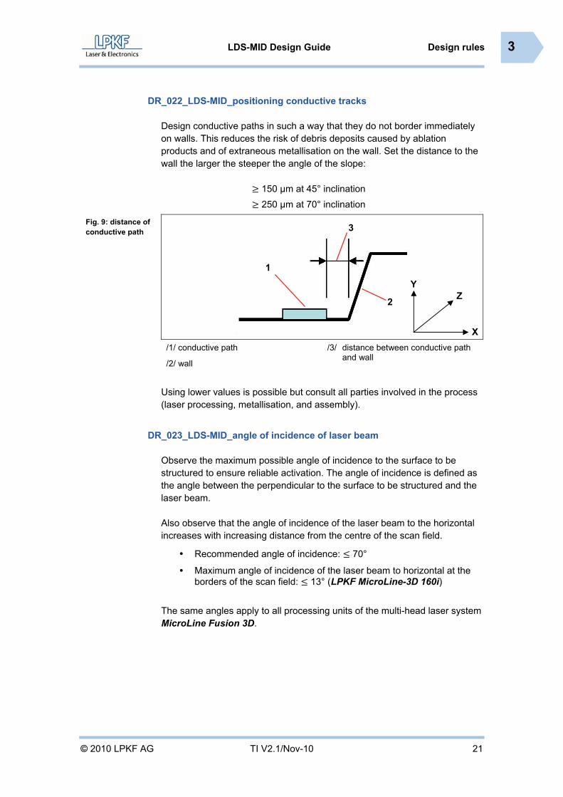
DR_022_LDS-MID_positioning conductive tracks
Design conductive paths in such a way that they do not border immediately on walls. This reduces the risk of debris deposits caused by ablation products and of extraneous metallisation on the wall. Set the distance to the wall the larger the steeper the angle of the slope: 150 μm at 45° inclination
250 μm at 70° inclination
Fig. 9: distance of conductive path
/1/ conductive path /3/ distance between conductive path
and wall /2/ wall
Using lower values is possible but consult all parties involved in the process (laser processing, metallisation, and assembly).
DR_023_LDS-MID_angle of incidence of laser beam
Observe the maximum possible angle of incidence to the surface to be structured to ensure reliable activation. The angle of incidence is defined as the angle between the perpendicular to the surface to be structured and the laser beam. Also observe that the angle of incidence of the laser beam to the horizontal increases with increasing distance from the centre of the scan field.
• Recommended angle of incidence: 70°
• Maximum angle of incidence of the laser beam to horizontal at the borders of the scan field: 13° (LPKF MicroLine-3D 160i)
The same angles apply to all processing units of the multi-head laser system MicroLine Fusion 3D.
1
Z
X
Y
3
2

Design rules LDS-MID Design Guide
22 TI V2.1/Nov-10 2010 LPKF AG
3
Fig. 10: angle of incidence
/1/ laser beam /4/ perpendicular to the surface to be
structured /2/ component
/3/ wall /5/ angle of incidence
Fig. 11: scan field
/1/ distance to centre /3/ angle of incidence (13 °) to the
horizontal
/2/ scan field /4/ deflected laser beam
DR_024_LDS-MID_ventilation
When designing the MID component, provide ventilation for hydrogen bubbles that are generated during metallisation. Observe the orientation of the component on the rack (if using rack metallisation) and create a design that ensures unhindered release of these hydrogen bubbles thus ensuring that metal layer growth is not impaired. For economic reasons (increased expenses for wastewater management), do not design components with cavities that have openings only on one side. Avoid e.g. blind holes.
DR_025_LDS-MID_fastening the plastic components
If the components cannot or are not intended to be retained in drums or baskets, provide clasping facilities e.g. ears, pickup holes, or undercuts for fastening the plastic components to the racks in the metallisation process.
2 Z
X
Y
1 5
4
5
1
2
3
4

LDS-MID Design Guide Design rules
2010 LPKF AG TI V2.1/Nov-10 23
3
DR_026_LDS-MID_recessed conductive paths
When metallising LDS MID components as loose material, devise recessed conductive paths if possible, thus preventing damage caused by grinding among the components especially on edges. Spacers on the MID component such as bumps or domes can prevent sticking together in drums. Devise the geometrical design in such a way that the components cannot jam each other in the drum process.
DR_027_LDS-MID_SMD assembly process
If the MID components are intended for surface mounting, observe the following basic design rules for mounting and connecting techniques:
• Place components on flat surfaces; these surfaces may even be on different levels. Reserve the slopes that connect the mounting surfaces for conductive paths. Other design concepts are possible but consult your assembly service provider or his systems manufacturer on this matter.
• Provide sufficient spacing of the landing pads towards the MID component edges and walls to ensure freedom of movement for the solder paste dispenser and the vacuum pick&place tip.
• Do not exceed tolerance measures of 50 μm for planar mounting pads when designing for dispenser or mounting systems without automated measuring of the component position. This imposes high demands on the quality of the injection moulded component.
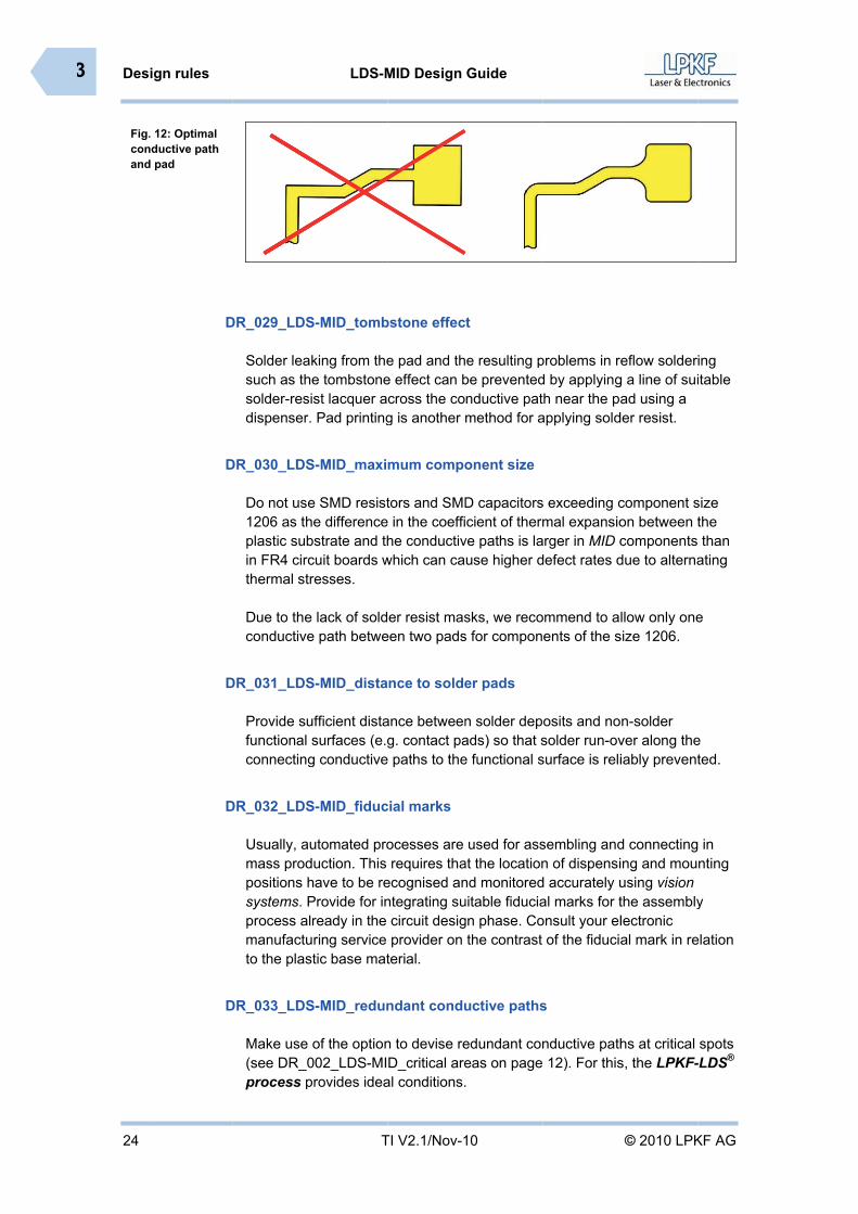
DR_028_LDS-MID_turns of paths
Avoid sharp-edged turns of conductive paths. Design turns with sufficiently wide radii (see Fig. 12: Optimal conductive path and pad on page 24) to reduce stress on the MID component in use. Especially the default settings of classic PCB routing programs are unsuitable for designing the conductive paths on LDS MID components. Observe the following items already when designing:
• Design smooth transitions of conductive paths to SMD component pads instead of abrupt transitions that are common in PCB technology. This applies especially if a solder-resist mask cannot be used or only with great effort (as is often the case with MID components) for this measure reduces the capillary effect that causes solder outflow from the pads to the conductive paths when the solder paste is melted.
• Round off the corners of SMD pads to reduce the risk of peeling under the thermal stress that impacts the MID assembly during the soldering process.
3 Desig
24
3
Fig. 1condand p
gn rules
12: Optimal ductive path pad
D
D
D
D
D
DR_029_LDS Solder leasuch as thsolder-resdispenser.
DR_030_LDS Do not use1206 as thplastic subin FR4 circthermal str Due to theconductive
DR_031_LDS Provide sufunctional connecting
DR_032_LDS Usually, aumass prodpositions hsystems. Pprocess almanufactuto the plas
DR_033_LDS Make use (see DR_0process p
LDS-M
T
S-MID_tomb
king from thehe tombstoneist lacquer a. Pad printing
S-MID_maxi
e SMD resisthe differencebstrate and thcuit boards wresses.
e lack of solde path betwe
S-MID_dista
ufficient distasurfaces (e.gg conductive
S-MID_fiduc
utomated production. This have to be reProvide for inlready in the uring service stic base mat
S-MID_redun
of the option002_LDS-MIprovides idea
MID Design
TI V2.1/Nov-1
bstone effec
e pad and the effect can bcross the cog is another
mum compo
tors and SMD in the coeffihe conductiv
which can ca
er resist maseen two pads
nce to solde
ance betweeng. contact pa paths to the
cial marks
ocesses are requires tha
ecognised anntegrating sucircuit desigprovider on
terial.
ndant condu
n to devise reD_critical are
al conditions.
Guide
10
t
e resulting pbe preventednductive patmethod for a
onent size
D capacitorscient of therm
ve paths is lause higher d
sks, we recos for compon
er pads
n solder depads) so that se functional s
used for assat the locationnd monitoreduitable fiduciagn phase. Cothe contrast
uctive paths
edundant coneas on page.
problems in rd by applyingh near the p
applying sold
s exceeding cmal expansio
arger in MID cdefect rates d
ommend to aents of the s
osits and nosolder run-ovsurface is reli
sembling andn of dispensid accurately ual marks for tonsult your el
of the fiduci
s
nductive path 12). For this
2010 LPK
eflow solderg a line of suiad using a
der resist.
component son between tcomponents due to alterna
llow only onesize 1206.
n-solder ver along theiably prevent
d connectinging and mouusing vision the assemblylectronic al mark in re
hs at critical s, the LPKF-
KF AG
ing itable
size the than
ating
e
e ted.
in nting
y
elation
spots -LDS®

LDS-MID Design Guide Design rules
2010 LPKF AG TI V2.1/Nov-10 25
3
DR_034_LDS-MID_reflow soldering method Also keep in mind the selection of the reflow soldering method already when designing the component.
• Watch out for possible hot-spots at elevated structures or at walls facing the heat sources when employing infrared or convection reflow soldering.
• If you are using the vapour phase soldering method, which is generally recommendable for MID technology, provide good drainage for the soldering medium (Galden) to prevent long evaporation periods after the reflow process.
• Another option is selective laser soldering using optical process control.
DR_035_LDS-MID_encapsulating
Depending on the application of the fully assembled LDS MID components, one of several options for encapsulating the finished assembly can be selected.
• Various producers offer several potting resins and protective lacquers that can either provide full protection or, if applied partially, protection of selected circuit areas.
• Hot-melt potting is an interesting manufacturing option to protect the MID assembly from environmental impact.
• A very interesting option for hermetically encapsulating MID assemblies is also laser welding if a laser-transparent material is selected for the "shell". Further information on process technology is available from our business unit plastic welding in Erlangen, Germany (www.laserquipment.de).

Design rules LDS-MID Design Guide
26 TI V2.1/Nov-10 2010 LPKF AG
3
LDS-MID Design Guide Injection moulding
2010 LPKF AG TI V2.1/Nov-10 27
4
Pos: 6 /ED_Technische_Dokumentation/7_Design_Guides/MID_Systeme/LDS_Design_Guide/Kapitel_4_Spritzguss/4_1_Werkzeugbau @ 0\mod_1287993436071_2058.docx @ 11305 @ 12333
4 Injection moulding
4.1 Tool design
4.1.1 Material
Do not use injection moulding tools made of aluminium to avoid tool-related extraneous plating during metallisation of the LDS MID components. Steel grades that can be through-hardened like 1.2343 or 1.2767 have proved suitable for processing LDS materials.
4.1.2 Tool surface
A standard surface finish (Rz 5 μm) is sufficient, polishing the surface usually is not necessary. However, for areas of the MID component which will be used for bonding, we recommend a partial polish of the tool using specific laser parameters for bonding areas. When designing the tool, ensure that tool temperature can be kept even over time and over the all tool surfaces.
4.1.3 Design rules for sprue and gate
Observe the following rules for designing sprue and gate:
1. Preferably use direct conical runners to the centre of the component.
2. Place the gate at the thickest wall of the component.
3. Always provide a means for intercepting the cold slug.
4. Devise the sprue bushing wider than the thickest component wall.
5. Provide a gate width of at least 50% of thickest component wall.
6. Prevent jetting by employing a large-diameter gate and shooting against a wall.
7. If more than one gate is required, observe the forming of weld lines!
When using multi-cavity tools, use sensors measuring the pressure inside the tool that are linked to the moulding system's control to ensure consistent quality over all cavities.

Injection moulding LDS-MID Design Guide
28 TI V2.1/Nov-10 2010 LPKF AG
4
Pos: 7 /ED_Technische_Dokumentation/7_Design_Guides/MID_Systeme/LDS_Design_Guide/Kapitel_4_Spritzguss/4_2_Spritzgussprozess @ 0\mod_1287993437931_2058.docx @ 11310 @ 2
4.2 Injection moulding process
Before injection-moulding an LDS MID lot, thoroughly remove residues of previous injection moulding processes to avoid contamination. Do not use mould release agents, especially those based on silicone for injection moulding. Avoid using lubricants for ejector pins or only use very sparingly. Observe the process window specified by the granulate manufacturers in the processing information as well as the instructions for pre-drying of the material. Avoid process interruptions to ensure consistent quality.
Pos: 8 /ED_Technische_Dokumentation/7_Design_Guides/MID_Systeme/LDS_Design_Guide/Kapitel_4_Spritzguss/4_3_Teilehandhabung @ 0\mod_1287993439587_2058.docx @ 11315 @ 233
4.3 Handling, packaging, and storage
4.3.1 Handling
Avoid damage and contamination (e.g. metal or skin contact, scratches) especially on critical areas when handling LDS MID components.
4.3.2 Packaging and storage
Provide adequate trays for the components removed from the mold and adequate packaging for further transport. Deep-drawn plastic trays have proved to be best and can form the basis of a consistent transport concept. Bear in mind the possible effects of packaging materials on subsequent processes (laser processing, metallisation, soldering, conductive adhesive bonding etc.). Prevent any water absorption of the LDS MID components during storage.

LDS-MID Design Guide Laser Processing
2010 LPKF AG TI V2.1/Nov-10 29
5
Pos: 9 /ED_Technische_Dokumentation/7_Design_Guides/MID_Systeme/LDS_Design_Guide/Kapitel_5_Laserbearbeitung/5_1_Laserbearbeitung @ 0\mod_1287993448025_2058.docx @ 11320 @ 12333
5 Laser Processing
5.1 Data Preparation
5.1.1 Avoid short fill vectors
Avoid short fill vectors. Fill narrow conductive paths lengthwise instead (see Fig. 13: Fill vectors). If an LDS MID component is to be structured with different slopes, different laser parameter sets may be necessary for the different areas to achieve reliable activation (see Fig. 14: Parameter sets). Observe, though, that the dynamic range of the optical Z-axis is not exceeded.
Fig. 13: Fill vectors
/1/ outline of conductive path
Fig. 14: Para-meter sets
/1/ parameter set 1 /2/ parameter set 2
1
Z
X
Y
1
2

Laser Processing LDS-MID Design Guide
30 TI V2.1/Nov-10 2010 LPKF AG
5
5.1.2 Laser parameters
The frequency is also limited by the maximum focus-tracking speed in Z-direction: The more inclined the slope the faster the focus has to be adjusted in Z-direction when processing. The maximum focus tracking speed of a MicroLine-3D 160i system of 1,000 mm/s results in a maximum travel speed of 1,500 mm/s on a 45° slope (see Fig. 15: Travel speed).
Fig. 15: Travel speed
/1/ angle of the slope = /3/ speed Z-direction = vz
/2/ resulting speed = v /4/ speed X-direction = vx
The calculation formula for the speed on the slope is:
For vz(max) = 1,000 mm/s and (max) = 45°, the resulting speed v on the slope is:
5.1.3 Other process parameters
Observe the instructions of the laser system's manufacturer when computing the suitable process parameters for average laser power and longitudinal and lateral inclination For the laser data preparation, we offer comprehensive training and training videos for the 3D software CircuitPro 3D to our customers of the new LPKF Fusion 3D system.
1
2
3
4

LDS-MID Design Guide Laser Processing
2010 LPKF AG TI V2.1/Nov-10 31
5
Pos: 10 /ED_Technische_Dokumentation/7_Design_Guides/MID_Systeme/LDS_Design_Guide/Kapitel_5_Laserbearbeitung/5_2_Laserbearbeitungsprozess @ 0\mod_1287993449775_2058.docx @ 11325 @ 233
5.2 Laser Processing
5.2.1 Fixture
If possible, employ plastic fixtures or clamping devices for laser processing of the LDS MID component to prevent extraneous plating during metallisation. If the components have to be clamped several times in different positions for laser processing, provide recesses on the fixture or clamping device to prevent damaging areas that are already activated when clamping in the subsequent position.
5.2.2 Positioning
Using an optical system (vision system) for aligning the conductive pattern on the component can compensate tolerances that can be caused by the fixture/clamping device, scanner mirrors, positioning systems etc. Fixture design rules help construct specific component fixtures. They are available to our laser system customers at no charge.
Pos: 11 /ED_Technische_Dokumentation/7_Design_Guides/MID_Systeme/LDS_Design_Guide/Kapitel_5_Laserbearbeitung/5_3_Teilehandhabung @ 0\mod_1287993451525_2058.docx @ 11330 @ 2333
5.3 Handling, packaging, and storage
5.3.1 Handling
Avoid damage and contamination (e.g. metal or skin contact, scratches) during and after laser processing especially on activated areas when handling LDS MID components (see chapter 4.3 Handling, packaging, and storage on page 28). We recommend using lint-free cotton gloves for manual loading and unloading of the components to be structured or already structured and to clean the gloves regularly. Prolonged usage of gloves or finger cots made of latex has a critical impact on quality in the metallisation process as sweat tends to diffuse through the gloves or finger cots and thus creates residues on the components.
5.3.2 Packaging
Do not use paper containing sulphuric compounds as packaging for transport to the metallisation process step. Avoid direct sunlight and use silica gel for storage as humidity and temperature can affect activation.

Laser Processing LDS-MID Design Guide
32 TI V2.1/Nov-10 2010 LPKF AG
5
5.3.3 Storage
Storing the laser-activated components for several weeks before metallisation poses no problem for the metallisation process if normal storage conditions (10 – 20° C, 65 % relative humidity) maintained. Avoid storing the components in conditions where condensation in combination of temperatures below 0° C can occur or in industrial (corrosive) atmosphere. Store only for as short as possible if these conditions cannot be avoided.

LDS-MID Design Guide Metallisation
2010 LPKF AG TI V2.1/Nov-10 33
6
Pos: 12 /ED_Technische_Dokumentation/7_Design_Guides/MID_Systeme/LDS_Design_Guide/Kapitel_6_Metallisierung/6_1_Teilehalterung @ 0\mod_1287993459634_2058.docx @ 11335 @ 12
6 Metallisation
6.1 Component retainers
Consider the suitability for your component and consult your metallisation service provider when deciding on the metallisation method (drum, basket, or rack metallisation) and on the type of rack or mesh size of drums or baskets. When using racks or baskets, use types that are fully insulated with thermoplastic fluorinated hydrocarbon compounds (Halar®) in a whirl-sintering process and clean them of extraneous metallisations regularly.
Pos: 13 /ED_Technische_Dokumentation/7_Design_Guides/MID_Systeme/LDS_Design_Guide/Kapitel_6_Metallisierung/6_2_Reinigung_der_LDS_MID @ 0\mod_1287993461337_2058.docx @ 11340 @ 2
6.2 Cleaning LDS MIDs
It is essential that the ablation products of the laser structuring that are highly activated and can cause massive problems in the form of extraneous plating are removed to ensure trouble-free further processing. Removal can be achieved in ultrasonic baths, using high-pressure water jet, or – if utmost cleanliness is required – by using CO2 snow-jet cleaning (for details on this technology refer to the web site of acp-micron: www.acp-micron.com) and can be done directly after laser processing or – more typically – before the plating steps. Common media for cleaning in ultrasonic baths (recommended frequency: 40 kHz) are aqueous tenside solutions such as Mucasol or Tickopur (both only available in Europe) as well as aqueous alcoholic tenside solutions (e.g. Tickopur + isopropyl alcohol). As the market for cleaning agents is structured regionally, we recommend consulting your supplier of the copper/nickel/gold chemicals for selecting the suitable cleaning chemicals. Please observe that the chemical properties of the cleaning agent can have negative effects on the platability of LDS MIDs. Conduct a series of tests investigating such effects.
Pos: 14 /ED_Technische_Dokumentation/7_Design_Guides/MID_Systeme/LDS_Design_Guide/Kapitel_6_Metallisierung/6_3_Elektrolyte_zur Metallisierung @ 0\mod_1287993463040_2058.docx @ 11345 @ 2

Metallisation LDS-MID Design Guide
34 TI V2.1/Nov-10 2010 LPKF AG
6
6.3 Electrolytes for metallisation
Observe the storage and operating instructions provided by the producers of the electroless plating chemicals (see overview of known electroless copper baths suitable for the LDS® process). Consider the transport chain and determine whether temperature-controlled transport is necessary. Observe shelf life and service life of the electrolytes. The following table shows the applicability of the individual copper baths for:
1 applicable as a copper strike bath for PC and PC/ABS in a two-stage process
2 applicable as full-build copper bath for PC and PC/ABS in a two-stage process
3 applicable as a single-stage copper bath (for LCP, PA, PBT, PBT/PET, PPA)
Table 5: Applicability of copper baths
copper bath producer 1 2 3
Circuposit 4500 www.rohm-haas.com
no yes yes
Cuposit 71-HS (formerly XP 6870)
yes* yes yes
M-Copper 85 www.mac-dermid.com
yes no no
Macuplex MID Copper
- yes yes
Macuplec 85 MX-LDS
yes* yes -
MID Copper 100 yes yes yes
Cupralux INI www.ato-tech.com
yes* yes yes
Enplate MID Select 9070
www.cookson-electronics.com
yes no no
Enplate Cu 872 no yes yes
Enplate LDS 400 (under development)
yes* yes -
Cupro-Coat 100 www.aimt-group.com
- yes yes
*under special conditions Pos: 15 /ED_Technische_Dokumentation/7_Design_Guides/MID_Systeme/LDS_Design_Guide/Kapitel_6_Metallisierung/6_4_1_Metallisierungsprozess @ 0\mod_1287993464853_2058.docx @ 11350 @ 23

LDS-MID Design Guide Metallisation
2010 LPKF AG TI V2.1/Nov-10 35
6
6.4 Metallisation Process
6.4.1 Processing order
Avoid unnecessary storage times after laser processing by metallising those components first that have been laser-processed first (first-in-first-out principle). Consult the electrolyte producer's processing information to determine the process window. Monitor by analysis and add the individual bath chemicals regularly to ensure a reproducible initial plating and constant deposition. Provide for sufficient movement of the components. Operate the baths at optimum load, especially for chemical copper deposition. We recommend a filter cycle for each bath using filter cartridges of pore sizes 5 μm.
Pos: 16 /ED_Technische_Dokumentation/7_Design_Guides/MID_Systeme/LDS_Design_Guide/Kapitel_6_Metallisierung/6_4_2_Beschichtung @ 0\mod_1287993466603_2058.docx @ 11355 @ 3
6.4.2 Metallisation processes/process steps
Execute the individual metallisation steps wet-on-wet, while providing good rinsing after each process step to preserve the service life of the individual baths. We recommend to devise the last rinsing step after the metallisation processes as a hot rinse (approx. 90°C with conductivity < 1 μS/cm, i.e. de-ionised water) and dry the components in circulating air to ensure spotless drying of the components for trouble-free assembly. The following list shows the most important process steps for a standard LDS metallisation:
Table 6: Steps in metallisation
Step Description
1 Pre-cleaning as described in section 6.2 Cleaning LDS MIDs
2 Copper bath or baths as a single- or two-stage process (strike + full build) – copper process depending on LDS material and bath chemicals used
3 MicroEtch
4 Pd activation
5 nickel bath (two-stage if necessary, depending on layer requirements)
6 gold bath
7 hot rinse
8 drying
Insert an adequate static and flow rinsing combination after each process bath (active bath) listed. LPKF provides laser system customers who are interested in entering the metallisation of LDS components with detailed design recommendations for entire metallisation systems for prototyping as well as for mass production. Please ask the LPKF sales representative.
Pos: 17 /ED_Technische_Dokumentation/7_Design_Guides/MID_Systeme/LDS_Design_Guide/Kapitel_6_Metallisierung/6_5_Temperung @ 0\mod_1287993468462_2058.docx @ 11360 @ 2
Metallisation LDS-MID Design Guide
36 TI V2.1/Nov-10 2010 LPKF AG
6
6.5 Thermal conditioning
In many cases, a thermal conditioning of the MID components after metallisation and before mounting and connection processes can achieve a better strength of the metal-plastic bond. A thermal conditioning at 120°C for one hour has proved good results for consolidation of the metallised MID component except for PC/ABS materials. Condition PC/ABS thermally at temperatures < 85°C but for a longer period.
Pos: 18 /ED_Technische_Dokumentation/7_Design_Guides/MID_Systeme/LDS_Design_Guide/Kapitel_6_Metallisierung/6_6_Handhabung @ 0\mod_1287993470150_2058.docx @ 11365 @ 2
6.6 Handling
Avoid damages as well as contaminations (e.g. scratches, metal and skin contact) especially on metallised spots when handling metallised LDS MID components. Provide suitable packaging, depending on the component with component separation (e.g. deep-drawn trays). Pay attention possible effects of packaging materials on subsequent processes (soldering, gluing etc.). Avoid electrostatic charging by the packaging material, especially before mounting the LDS MID components. The decision whether to use ESD packaging depends on the circuit technology of the assembly and its ESD susceptibility; consult your service provider for mounting and bonding.

LDS-MID Design Guide Quality assurance
2010 LPKF AG TI V2.1/Nov-10 37
7
Pos: 19 /ED_Technische_Dokumentation/7_Design_Guides/MID_Systeme/LDS_Design_Guide/Kapitel_7_Qualitätsprüfung/7_Qualitätsprüfung @ 0\mod_1287993478993_2058.docx @ 11370 @ 1
7 Quality assurance We recommend developing a process FMEA before planning the production process steps in order to derive and define the necessary gates for quality assurance measures. The LDS QA matrix indicates possible test methods for manufacturing LDS MIDs. These as well as images of defects in the individual process steps are part of the system documentation in the delivery of MicroLine-3D laser systems.
Quality assurance LDS-MID Design Guide
38 TI V2.1/Nov-10 2010 LPKF AG
7

LDS-MID Design Guide Appendix
2010 LPKF AG TI V2.1/Nov-10 39
8
Pos: 20 /ED_Technische_Dokumentation/7_Design_Guides/MID_Systeme/LDS_Design_Guide/Kapitel_8_Anhang/8_Abbildungsverzeichnis @ 0\mod_1287993480400_2058.docx @ 11375 @ 1222
8 Appendix
8.1 Table of figures
Fig. 1: Beveled ejector pin ................................................................................. 13 Fig. 2: Scan field volume ................................................................................... 14 Fig. 3: Dimensions of conductive paths ............................................................. 15 Fig. 5: Laser beam ............................................................................................. 18 Fig. 6: Passage .................................................................................................. 19 Fig. 7: Press-fit connector pin ............................................................................ 20 Fig. 8: edge radius ............................................................................................. 20 Fig. 9: distance of conductive path .................................................................... 21 Fig. 10: angle of incidence ................................................................................. 22 Fig. 11: scan field ............................................................................................... 22 Fig. 12: Optimal conductive path and pad ......................................................... 24 Fig. 13: Fill vectors ............................................................................................. 29 Fig. 14: Parameter sets ..................................................................................... 29 Fig. 15: Travel speed ......................................................................................... 30
8.2 List of tables
Table 1: Materials ................................................................................................ 9 Table 3: Design rules ......................................................................................... 11 Table 4: Finish surfaces ..................................................................................... 17 Table 5: Applicability of copper baths ................................................................ 34 Table 6: Steps in metallisation ........................................................................... 35
Appendix LDS-MID Design Guide
40 TI V2.1/Nov-10 2010 LPKF AG
8
8.3 List of abbreviations
A ABS acrylonitrile butadiene styrene
Ag silver
Al aluminium
ASIG auto-catalytic silver immersion gold
Au gold
C CAD computer aided design
CO2 carbon dioxide
CTE coefficient of thermal expansion
Cu copper
D DIN Deutsches Institut für Normung (German standards institute)
E ECAD electronic CAD
EG electroless Au
EN electroless Ni
EP electroless Pd
ESD electrostatic discharge
F FMEA failure modes and effects analysis
I IG immersion Au
IR infrared
L LCP liquid crystal polymer
LDS laser direct structuring
M MCAD mechanical CAD
MID moulded interconnect devices
N NiP nickel-phosphorus
P PA polyamide
PBT/PET polybutylene terephthalate/polyethylene terephthalate blend
PC polycarbonate
PCB printed circuit board
Pd palladium
PPA polyphthalamide
Q QA quality assurance
S Si silicon
SMD surface-mounted device
Sn tin

LDS-MID Design Guide Appendix
2010 LPKF AG TI V2.1/Nov-10 41
8
8.4 Conversion tables
Distance
1 cm = 0.3937 in. 1 inch (in) = 25.4 mm
1 mm = 39.37 mil 1 mil = 1/1000 in. = 2.54 x 10⁻² mm
Area
1 cm2 = 0.1550 sq. in. 1 sq. inch = 6.4516 cm2
1 m2 = 10.7639 sq.ft. 1 sq.ft. = 144 in.2 = 0.0929 m2
1 m2 = 1.19599 sq.yd. 1 sq. yd. = 9 ft.2 = 0.8361 m2
Temperature
- 20 °C = - 4 °F °F = °C * 1.8 + 32
0 °C = 32 °F °C = (°F - 32) / 1.8
100 °C = 212 °F
=== Ende der Liste für Textmarke Inhalt ===

Appendix LDS-MID Design Guide
42 TI V2.1/Nov-10 2010 LPKF AG
8