ldc1000-q1 inductance to digital converter datasheet … · connect this pin to an external lc...
TRANSCRIPT

Distance
LDC
Out
put (
Rp)
0.25 0.5 0.75
Product
Folder
Sample &Buy
Technical
Documents
Tools &
Software
Support &Community
LDC1000-Q1SLOS886B –SEPTEMBER 2014–REVISED OCTOBER 2014
LDC1000-Q1 Inductance to Digital Converter1 Features 3 Description
Inductive sensing is a contactless, short-range1• Qualified for Automotive Applications
sensing technology that enables low-cost, high-• AEC-Q100 Qualified With the Following Results: resolution sensing of conductive targets in the– Device Temperature Grade 0: –40°C to 150°C presence of dust, dirt, oil, and moisture, making this
Ambient Operating Temperature Range E technology extremely reliable in harsh environments.Using a coil that can be created for example on a– Device Temperature Grade 1: –40°C to 125°CPCB as a sensing element, the LDC1000-Q1 deviceAmbient Operating Temperature Range Qenables ultra-low cost system solutions.
– Device HBM ESD Classification Level 2Inductive sensing technology enables precise– Device CDM ESD Classification Level C6 measurement of linear or angular position,
• Magnet-Free Operation displacement, motion, compression, vibration, metalcomposition, and many other applications in markets• Sub-Micron Precisionincluding automotive, consumer, computer, industrial,• Adjustable Sensing Range (through Coil Design)medical, and communications. Inductive sensing
• Lower System Cost offers better performance and reliability at lower cost• Remote Sensor Placement (Decoupling the LDC than other competitive solutions.
from Harsh Environments) The LDC1000-Q1 device is the first automotive-• High Durability (by Virtue of Contact-Less qualified LDC, offering the benefits of inductive
Operation) sensing in a low-power, small-footprint solution. Theproduct is available in a 16-pin TSSOP package and• Insensitivity to Environmental Interference (suchoffers several modes of operation. An SPI interfaceas Dirt, Dust, Water, Oil)simplifies connection to an MCU.• Supply Voltage, Analog: 4.75 to 5.25 V
• Supply Voltage, IO: 1.8 to 5.25 V Device Information(1)
• Supply Current (Without LC Tank): 1.7 mA PART NUMBER PACKAGE BODY SIZE (NOM)• RP Resolution: 16-bit LDC1000-Q1 TSSOP (16) 5.00 mm × 4.40 mm
• L Resolution: 24-bit (1) For all available packages, see the orderable addendum atthe end of the data sheet.• LC Frequency Range: 5 kHz to 5 MHz
Typical Application — Axial Distance Sensing2 Applications• Drive-by-Wire Systems• Gear-Tooth Counting• Flow Meters• Push-Button Switches• Rotational Position Sensor• Linear Position Sensor• Pedal Position Sensor• Throttle Position Sensor
1
An IMPORTANT NOTICE at the end of this data sheet addresses availability, warranty, changes, use in safety-critical applications,intellectual property matters and other important disclaimers. PRODUCTION DATA.

LDC1000-Q1SLOS886B –SEPTEMBER 2014–REVISED OCTOBER 2014 www.ti.com
Table of Contents7.3 Feature Description................................................... 81 Features .................................................................. 17.4 Device Functional Modes........................................ 122 Applications ........................................................... 17.5 Programming........................................................... 143 Description ............................................................. 17.6 Register Map........................................................... 164 Revision History..................................................... 2
8 Application and Implementation ........................ 265 Pin Configuration and Functions ......................... 38.1 Application Information............................................ 266 Specifications......................................................... 48.2 Typical Application ................................................. 286.1 Absolute Maximum Ratings ...................................... 4
9 Power Supply Recommendations ...................... 326.2 Handling Ratings....................................................... 410 Layout................................................................... 326.3 Recommended Operating Conditions....................... 4
10.1 Layout Guidelines ................................................. 326.4 Thermal Information .................................................. 410.2 Layout Example .................................................... 336.5 Electrical Characteristics........................................... 5
11 Device and Documentation Support ................. 346.6 Timing Requirements ................................................ 611.1 Trademarks ........................................................... 346.7 Typical Characteristics .............................................. 711.2 Electrostatic Discharge Caution............................ 347 Detailed Description .............................................. 811.3 Glossary ................................................................ 347.1 Overview ................................................................... 8
12 Mechanical, Packaging, and Orderable7.2 Functional Block Diagram ......................................... 8Information ........................................................... 34
4 Revision History
Changes from Revision A (September 2014) to Revision B Page
• Changed pin configuration image and removed DAP from Pin Functions table .................................................................... 3
Changes from Original (September 2014) to Revision A Page
• Changed the device status from Product Preview to Production Data ................................................................................. 1
2 Submit Documentation Feedback Copyright © 2014, Texas Instruments Incorporated
Product Folder Links: LDC1000-Q1

SCLK
CSB
SDI
VIO
SDO
DGND
CFB
CFA INA
INB
GND
VDD
CLDO
TBCLK/XIN
XOUT
INTB1
2
3
4
5
6
7
8
16
15
14
13
12
11
10
9
LDC1000-Q1www.ti.com SLOS886B –SEPTEMBER 2014–REVISED OCTOBER 2014
5 Pin Configuration and Functions
PW Package16-Pin TSSOP
Top View
Pin FunctionsPIN
TYPE (1) DESCRIPTIONNO. NAME1 SCLK DI SPI clock input. The SCLK pin is used to clock-out and clock-in the data from or into the chip
SPI CSB. Multiple devices can be connected on the same SPI bus and the CSB pin can be used to2 CSB DI select which device is communicated with.SPI Slave Data In (Master Out Slave In). This pin should be connected to the Master Out Slave In of3 SDI DI the master device.
4 VIO P Digital IO Supply5 SDO DO SPI Slave Data Out (Master In Slave Out). This pin is high-Z when the CSB pin is high.6 DGND P Digital ground7 CFB A LDC filter capacitor8 CFA A LDC filter capacitor9 INA A External LC Tank. Connect this pin to an external LC tank.10 INB A External LC Tank. Connect this pin to an external LC tank.11 GND P Analog ground12 VDD P Analog supply13 CLDO A LDO bypass capacitor. Connect a 56-nF capacitor from this pin to GND.14 TBCLK/XIN DI/A External time-base clock and XTAL. This pin is either an external clock or is connected to a crystal.
XTAL. Crystal out. Connecting an 8-Mhz crystal between the TBCLK/XIN pin and the XOUT pin with15 XOUT A 20-pF capacitor from each pin to ground is recommended. This pin should be floating when an
external clock is used.Configurable interrupt. This pin can be configured to function in three different ways (threshold detect,16 INTB DO wakeup, or DRDYB) by programing the INT pin mode register.
(1) DO: Digital Output, DI: Digital Input, P: Power, A: Analog
Copyright © 2014, Texas Instruments Incorporated Submit Documentation Feedback 3
Product Folder Links: LDC1000-Q1

LDC1000-Q1SLOS886B –SEPTEMBER 2014–REVISED OCTOBER 2014 www.ti.com
6 Specifications
6.1 Absolute Maximum Ratingsover operating free-air temperature range (unless otherwise noted) (1)
MIN MAX UNITAnalog supply voltage VDD – GND 5.5 VIO supply voltage VIO – GND 5.5 VVoltage On any pin –0.3 VDD + 0.3 V
On any digital pin –0.3 VIO + 0.3 VInput Current INA and INB 8 mAJunction Temperature, TJ 150 °C
(1) Stresses beyond those listed under Absolute Maximum Ratings may cause permanent damage to the device. These are stress ratingsonly, which do not imply functional operation of the device at these or any other conditions beyond those indicated under RecommendedOperating Conditions. Exposure to absolute-maximum-rated conditions for extended periods may affect device reliability.
6.2 Handling RatingsMIN MAX UNIT
Tstg Storage temperature range –65 150 °CHuman body model (HBM), per AEC Q100-002 (1) –2000 2000
V(ESD) Electrostatic discharge VCharged device model (CDM), per AEC Q100-011, all pins –1000 1000
(1) AEC Q100-002 indicates HBM stressing is done in accordance with the ANSI/ESDA/JEDEC JS-001 specification.
6.3 Recommended Operating Conditionsover operating free-air temperature range (unless otherwise noted)
MIN MAX UNITVDD Analog supply voltage (VDD – GND) 4.75 5.25 VVIO IO supply voltage (VIO – GND) 1.8 5.25 V
VDD – VIO ≥0 VOperating temperature (see the Mechanical, Grade 0 (temperature range E) –40 150
TA Packaging, and Orderable Information section for °CGrade 1 (temperature range Q) –40 125package options)
6.4 Thermal InformationPW
THERMAL METRIC (1) UNIT16 PINS
RθJA Junction-to-ambient thermal resistance 106.3RθJC(top) Junction-to-case (top) thermal resistance 40.8RθJB Junction-to-board thermal resistance 51.3
°C/WψJT Junction-to-top characterization parameter 3.6ψJB Junction-to-board characterization parameter 50.8RθJC(bot) Junction-to-case (bottom) thermal resistance —
(1) For more information about traditional and new thermal metrics, see the IC Package Thermal Metrics application report, SPRA953.
4 Submit Documentation Feedback Copyright © 2014, Texas Instruments Incorporated
Product Folder Links: LDC1000-Q1

LDC1000-Q1www.ti.com SLOS886B –SEPTEMBER 2014–REVISED OCTOBER 2014
6.5 Electrical CharacteristicsUnless otherwise specified, all limits ensured for TA = 25°C, VDD = 5 V, VIO = 3.3 V
PARAMETER TEST CONDITIONS MIN TYP MAX UNITPOWERVDD Analog supply voltage 4.75 5 5.25 VVIO IO supply voltage VIO ≤ VDD 1.8 3.3 5.25 V
Does not include the LCIDD Supply current 1.7 2.3 mAtank currentIIO IO supply current Static current 14 µAIDD(LP) Low-power mode supply current Without LC tank 250 µA
From POR to ready-to-t(start) Start-up time convert. Crystal not used 2 ms
for frequency counterLDCfsensor_min Minimum sensor frequency 5 kHzfsensor_max Maximum sensor frequency 5 MHzAsensor_min Minimum sensor amplitude 1 VPP
Asensor_max Maximum sensor amplitude 4 VPP
Oscillation start-up timetrec Recovery time after RP under-range 10 1 / fsensor
conditionZRP_min Minimum sensor RP range 798 ΩRRP_max Maximum sensor RP range 3.93 MΩRRP_res RP measurement resolution 16 Bits
Minimum programmabletres(min) Minimum response time 192 × 1 / fsensor ssettling time of digital filterMaximum programmabletres(max) Maximum response time 6144 × 1 / fsensor ssettling time of digital filter
EXTERNAL CLOCK AND CRYSTAL FOR FREQUENCY COUNTERfref Crystal frequency 8 MHztxtalst Crystal startup time 30 ms
External clock frequency 8 MHzExternal clock input high voltage VIO V
DIGITAL I/O CHARACTERISTICS0.8 ×VIH Logic 1 input voltage VVIO
VIL Logic 0 input voltage 0.2 × VIO VVOH Logic 1 output voltage I(SOURCE) = 400 µA VIO– 0.3 VVOL Logic 0 output voltage I(SINK) = 400 µA 0.3 VIlkgIO Digital IO leakage current –500 500 nA
Copyright © 2014, Texas Instruments Incorporated Submit Documentation Feedback 5
Product Folder Links: LDC1000-Q1

CSB
SDI
th(CS) tsu(CS)
16th Clock
SCLK
th(CS) tsu(CS)
D7 D1 D0
1st Clock 8th Clock
tthttODZtOZD
SCLK
SDI
ttwLt
Valid Data Valid Data
ttwHt
ttsut ttht
16th Clock
LDC1000-Q1SLOS886B –SEPTEMBER 2014–REVISED OCTOBER 2014 www.ti.com
6.6 Timing RequirementsUnless otherwise noted, all limits specified at TA = 25°C, VDD = 5 V, VIO = 3.3 V, 10-pF capacitive load in parallel with a 10-kΩload on the SDO. Specified by design; not production tested. See Figure 1
MIN NOM MAX UNITfSCLK Serial clock frequency See Figure 1 4 MHztwH SCLK pulse-width high fSCLK = 4 Mhz, See Figure 1 0.4 / fSCLK stwL SCLK pulse-width low fSCLK = 4 Mhz, See Figure 1 0.4 / fSCLK stsu SDI setup time 10 ns
See Figure 1th SDI hold time 10 ns
SDO driven-to-tristate Measured at 10% / 90% point, SeetODZ 20 nstime Figure 2SDO tristate-to-driven Measured at 10% / 90% point, SeetOZD 20 nstime Figure 2
td(OUTPUT) SDO output delay time 20 nstsu(CS) CSB setup time See Figure 2 20 nsth(CS) CSB hold time 20 nstIAG inter-access gap See Figure 16 100 ns
Data ready pulse at every 1 / ODR if notw(DRDY) Data ready pulse width 1 / fsensor sdata is read
Figure 1. Write Timing Diagram
Figure 2. Read Timing Diagram
6 Submit Documentation Feedback Copyright © 2014, Texas Instruments Incorporated
Product Folder Links: LDC1000-Q1

0
2
4
6
8
10
12
14
0 1 2 3 4 5 6 7 8
Rp
(k
Distance (mm) C002
0
10
20
30
40
50
60
0 1 2 3 4 5 6 7 8
Cod
e (d
ecim
al)
Distance (mm) C003
LDC1000-Q1www.ti.com SLOS886B –SEPTEMBER 2014–REVISED OCTOBER 2014
6.7 Typical Characteristics
Sensor Details: Table 21 Rp_MIN: 1.347 kΩ Sensor Details: Table 21 Rp_MIN: 1.347 kΩTarget Material: Stainless Steel Rp_MAX: 38.785 kΩ Target Material: Stainless Steel Rp_MAX: 38.785 kΩ
Figure 3. RP vs Distance Figure 4. Proximity Data vs Distance
Copyright © 2014, Texas Instruments Incorporated Submit Documentation Feedback 7
Product Folder Links: LDC1000-Q1

4-WireSerial
Interface
INA
INB
SCLK
SDI
SDO
INTB
VDD
CFA CFB
Power
GND VIO DGND CLDO
rs
L
C
Frequency Counter
TBCLK/XIN XOUT
ThresholdDetector
Frequency Counter Data
Register
Proximity DataRegister
LDC
CSB
LDC1000-Q1SLOS886B –SEPTEMBER 2014–REVISED OCTOBER 2014 www.ti.com
7 Detailed Description
7.1 OverviewThe LDC1000-Q1 device is an inductance-to-digital converter that simultaneously measures the impedance andresonant frequency of an LC resonator. The device accomplishes this task by regulating the oscillation amplitudein a closed-loop configuration to a constant level, while monitoring the energy dissipated by the resonator. Bymonitoring the amount of power injected into the resonator, the LDC1000-Q1 device can determine the value ofRP. When the value is determined, the device returns this as a digital value which is inversely proportional to RP.In addition, the LDC1000-Q1 device also measure the oscillation frequency of the LC circuit. This frequency isused to determine the inductance of the LC circuit. The device outputs a digital value that is inverselyproportional to frequency.
The threshold detector block provides a comparator with hysteresis. With the threshold registers programed andcomparator enabled, the proximity data register is compared with threshold registers and INTB pin indicates theoutput.
The device has a simple 4-wire SPI interface. The INTB pin provides multiple functions which are programmablewith SPI.
The device has separate analog and I/O supplies. The analog supply operates at 5 V and the I/O operates at 1.8to 5 V. The integrated LDO requires a 56-nF capacitor connected from the CLDO pin to GND.
7.2 Functional Block Diagram
7.3 Feature Description
7.3.1 Inductive SensingAn alternating current (AC) flowing through a coil generates an AC magnetic field. If a conductive material, suchas a metal target, is brought into the vicinity of the coil, this magnetic field induces circulating currents (eddycurrents) on the surface of the target. These eddy currents are a function of the distance, size, and compositionof the target. These eddy currents then generate a magnetic field that opposes the original field generated by thecoil. This mechanism is best compared to a transformer, where the coil is the primary core and the eddy currentis the secondary core. The inductive coupling between both cores depends on distance and shape. Hence theresistance and inductance of the secondary core (eddy current), shows up as a distant dependent resistive andinductive component on the primary side (coil). Figure 5 through Figure 8 show a simplified circuit model.
8 Submit Documentation Feedback Copyright © 2014, Texas Instruments Incorporated
Product Folder Links: LDC1000-Q1

C
Oscillator
L(d)
rs(d)
Target Metal Surface
Conductance of Metal
Ls + L(d)
rs + R(d)
Distance d
Eddy Currents
Metal Target
d
LDC1000-Q1www.ti.com SLOS886B –SEPTEMBER 2014–REVISED OCTOBER 2014
Feature Description (continued)
Figure 5. Inductor with a Metal Target
Eddy currents generated on the surface of the target can be modeled as a transformer as shown in Figure 6. Thecoupling between the primary and secondary coils is a function of the distance and characteristics of theconductor. In Figure 6, the inductance Ls is the inductance of the coil, and rs is the parasitic series resistance ofthe coil. The inductance L(d), which is a function of distance, d, is the coupled inductance of the metal target.Likewise, R(d) is the parasitic resistance of the eddy currents.
Figure 6. Metal Target Modeled as L and R With Circulating Eddy Currents
Generating an alternating magnetic field with just an inductor consumes a large amount of power. This powerconsumption can be reduced by adding a parallel capacitor, turning the right part of Figure 6 into a resonator asshown in Figure 7 . In this manner the power consumption is reduced to the eddy and inductor losses rs + R(d)only.
Figure 7. LC Tank Connected to Oscillator
The LDC1000-Q1 device does not directly measure the series resistance. Instead, the device measures theequivalent parallel resonance impedance RP (see Figure 8). This representation is equivalent to therepresentation shown in Figure 8 , where the parallel resonance impedance RP(d) is given by Equation 1.
Copyright © 2014, Texas Instruments Incorporated Submit Documentation Feedback 9
Product Folder Links: LDC1000-Q1

0
2
4
6
8
10
12
14
16
18
20
0 1 2 3 4 5 6 7 8
Distance (mm) C001
Equiv
ale
nt P
ara
llel
Resonance Im
pedance (
kΩ
)
C
Oscillator
L(d) RP(d)
LDC1000-Q1SLOS886B –SEPTEMBER 2014–REVISED OCTOBER 2014 www.ti.com
Feature Description (continued)
Figure 8. Equivalent Resistance of rs in Parallel With LC Tank
RP(d) = (1 ⁄ ([rs + R(d)]) × ([Ls + L(d)]) / C (1)RP = (1 / rs) × (L / C) (2)
Figure 9 shows the variation in RP as a function of distance for a 14-mm diameter PCB coil (23 turns, 4-mil tracewidth, 4-mil spacing between trace,1-oz copper thickness, FR4). The target metal used is a stainless steel 2-mmthick.
Figure 9. Typical RP versus Distance With a 14-mm PCB Coil
7.3.2 Measuring Parallel Resonance Impedance and Inductance with LDC1000-Q1The LDC1000-Q1 device is an inductance-to-digital converter that simultaneously measures the impedance andresonant frequency of an LC resonator. The device accomplishes this task by regulating the oscillation amplitudein a closed-loop configuration to a constant level, while monitoring the energy dissipated by the resonator. Bymonitoring the amount of power injected into the resonator, the LDC1000-Q1 device can determine the value ofRP. The device returns this value as a digital value which is inversely proportional to RP. In addition, theLDC1000-Q1 device can also measure the oscillation frequency of the LC circuit. This frequency is used todetermine the inductance of the LC circuit. The oscillation frequency is returned as a digital value.
The LDC1000-Q1 device supports a wide range of LC combinations with oscillation frequencies ranging from 5kHz to 5 MHz and RP ranging from 798 Ω to 3.93 MΩ. This range of RP can be viewed as the maximum inputrange of an ADC. As shown in Figure 9, the range of RP is typically much smaller than maximum input rangesupported by the LDC1000-Q1 device. To achieve better resolution in the desired sensing range, the LDC1000-Q1 device offers a programmable input range through the Rp_MIN and Rp_MAX registers. See the Calculationof Rp_Min and Rp_Max section for how to set these registers.
When the resonance impedance of the sensor, RP, drops below the programed Rp_MIN, the RP output of theLDC will clip at the full scale output. An example occurrence of this situation is when a target comes too close tothe coil.
10 Submit Documentation Feedback Copyright © 2014, Texas Instruments Incorporated
Product Folder Links: LDC1000-Q1

0
20
40
60
80
100
120
140
±1.0
0
±0.7
5
±0.5
0
±0.2
5
0.0
0
0.2
5
0.5
0
0.7
5
1.0
0
Count
Deviation (µm)C001
0.0
0.1
0.2
0.3
0.4
0.5
0.6
0.0 0.2 0.4 0.6 0.8 1.0 1.2
RM
SN
ois
e(µ
m)
Distance (mm) C001
0
5000
10000
15000
20000
25000
30000
12 17 22 27 32 37 42 47
Co
de
(de
cim
al)
C001Equivalent Parallel Resonance Impedance (kΩ)
LDC1000-Q1www.ti.com SLOS886B –SEPTEMBER 2014–REVISED OCTOBER 2014
Feature Description (continued)
Figure 10. Transfer Characteristics of LDC1000-Q1 With Rp_MIN = 16.160 kΩ and Rp_MAX = 48.481 kΩ
Use Equation 3 to calculate the resonance impedance from the digital output code.RP = (Rp_MAX × Rp_MIN ) / (Rp_MIN × (1 – Y) + Rp_MAX × Y), in Ω.
Where:• Y = Proximity Data / 215
• Proximity data is the LDC output, register address 0x21 and 0x22. (3)
Example: If Proximity data (address 0x22 to 0x21) is 5000, Rp_MIN is 2.394 kΩ, and Rp_MAX is 38.785 kΩ, theresonance impedance is given by:
Y = 5000 / 215 = 0.1526 (4)RP = (38785 × 2394) / (2394 × (1 – 0.1526) + 38785 × 0.1526) =(92851290) / (2028.675 + 5918.591) (5)RP = 11.683 kΩ (6)
Figure 11 and Figure 12 show the change in RMS noise versus distance and a histogram of noise, with thetarget at an 0.8-mm distance from the sensor coil. Data was collected with a 14-mm PCB coil (23 turns, 4-miltrace width, 4-mil spacing between trace,1-oz copper thickness, FR4) with a sensing range of 0.125 mm to 1.125mm. At a distance of 0.8 mm, the RMS noise is approximately 250 nm.
Figure 11. Typical RMS Noise versus Distance With PCBFigure 12. Histogram of Output Codes at 0.8-mm DistanceCoil
NOTEAlthough the LDC1000-Q1 device has high resolution, the absolute accuracy depends onoffset and gain correction which can be achieved by two-point calibration.
Copyright © 2014, Texas Instruments Incorporated Submit Documentation Feedback 11
Product Folder Links: LDC1000-Q1

LDC1000-Q1SLOS886B –SEPTEMBER 2014–REVISED OCTOBER 2014 www.ti.com
Feature Description (continued)7.3.2.1 Measuring InductanceThe LDC1000-Q1 device measures the frequency of the oscillation of the sensor by a frequency counter. Thefrequency counter timing is set by an external clock or crystal. Either the external clock (8 MHz typical) from amicrocontroller can be provided on the TBCLK/XIN pin or a crystal can be connected on the TBCLK/XIN andXOUT pins. The clock mode is controlled through clock configuration register (address 0x05). The sensorresonance frequency is derived from the frequency-counter register value (see the Frequency Counter LSB(offset = 0x23) [reset = NA] section through the Frequency Counter MSB (offset = 0x25) [reset = NA] section) asshown in Equation 7.
fsensor = (1/3) × (fext / fcount) × tres
where• fsensor is the sensor frequency• fext is the frequency of the external clock or crystal• fcount is the value obtained from the Frequency Counter Data register (see the Frequency Counter LSB (offset =
0x23) [reset = NA] section through the Frequency Counter MSB (offset = 0x25) [reset = NA] section)• tres is the programmed response time (see the LDC Configuration (offset = 0x04) [reset = 0x1B] section) (7)
The inductance in H can be calculated with Equation 8.L=1 / [C × (2 × π × fsensor)2]
where• C is the parallel capacitance of the resonator (8)
7.3.2.1.1 Example
If the following values are selected, fext = 6 Mhz, tres = 6144, C = 10 0pF, and measured fcount = 3000 (decimal)(see the Frequency Counter LSB (offset = 0x23) [reset = NA] section through the Frequency Counter MSB (offset= 0x25) [reset = NA] section) then:
fsensor = 1/3 × (6000000 / 3000) × (6144) = 4.096 MHz (9)
Now use Equation 10.L = 1 / [C × (2 × π × fsensor)2]
where• L = 15.098 µH (10)
The accuracy of measurement largely depends upon the choice of the external time-base clock (TBCLK) or thecrystal oscillator (XIN and XOUT).
7.4 Device Functional Modes
7.4.1 INTB Pin ModesThe INTB pin is a configurable output pin which can be used to drive an interrupt on an MCU. The LDC1000-Q1device provides three different modes on the INTB pin which include:1. Comparator mode2. Wake-up mode3. DRDY mode
The LDC1000-Q1 device has a built-in high trigger and low trigger threshold registers that can be a comparatorwith programmable hysteresis or a special mode that is used to wake-up an MCU. The following sectionsdescribe these modes in detail.
7.4.1.1 Comparator ModeIn the comparator mode, the INTB pin is asserted or de-asserted when the proximity register value increasesabove the threshold high registers or decreases below the threshold low registers respectively. In this mode, thefunction of the LDC1000-Q1 device is a proximity switch with programmable hysteresis.
12 Submit Documentation Feedback Copyright © 2014, Texas Instruments Incorporated
Product Folder Links: LDC1000-Q1

RP Data
t
SPI SPI: INTB pin mode changed to DRDYB
CSB
INTB
Threshold High
Threshold Low
Threshold High
Threshold Low
INTB
RP Data
t
LDC1000-Q1www.ti.com SLOS886B –SEPTEMBER 2014–REVISED OCTOBER 2014
Device Functional Modes (continued)
Figure 13. Behavior of the INTB Pin in Comparator Mode
7.4.1.2 Wake-Up ModeIn wake-up mode, the INTB pin is asserted when proximity register value increases above the threshold highregisters and is deasserted when wake-up mode is disabled in the INTB pin mode register.
This mode can wake-up an MCU that is in sleep mode to conserve power.
Figure 14. Behavior of the INTB Pin in Wake-Up Mode
7.4.1.3 DRDYB ModeIn DRDY mode (default), the INTB pin is asserted every time the conversion data is available and is deassertedwhen the read command on register 0x21 is registered internally. If the read command is in progress, the pin ispulsed instead.
Copyright © 2014, Texas Instruments Incorporated Submit Documentation Feedback 13
Product Folder Links: LDC1000-Q1

CSB
SDI
SCLK
Read DATA
1
tDATA FIELDt
SDO
R/Wb A6 A5 A4 A3 A2 A1 A0 Write DATA
2 3 4 5 6 7 8 9 10 11 12 13 14 15 16 17
tCOMMAND FIELDt
High-Z
tSingle Access Cyclet
Data (8-bits)
C6C7 C5 C4 C3 C2 C1 C0 D7(MSB)
D6 D5 D4 D3 D2 D1 D0(LSB)
D7(MSB)
D6 D5 D4 D3 D2 D1 D0(LSB)
Address (7-bits)R/Wb = Read/Write0: Write Data1: Read Data
tIAG
t
SPI Data Read
CSB
INTB
tODRt
CMD:Read 0x21
LDC1000-Q1SLOS886B –SEPTEMBER 2014–REVISED OCTOBER 2014 www.ti.com
Device Functional Modes (continued)
Figure 15. Behavior of the INTB Pin in DRDYB Mode
7.5 Programming
7.5.1 Digital InterfaceThe LDC1000-Q1 device uses a 4-wire SPI interface to access control and data registers. The LDC1000-Q1device is an SPI slave device and does not initiate any transactions.
7.5.1.1 SPI DescriptionA typical serial interface transaction begins with an 8-bit instruction that is comprised of a read-write (R/W) bit(MSB, R = 1) and a 7-bit address of the register followed by a data field that is typically 8 bits. However, the datafield can be extended to a multiple of 8 bits by providing sufficient SPI clocks. See the Extended SPITransactions section.
Figure 16. Serial Interface Protocol
14 Submit Documentation Feedback Copyright © 2014, Texas Instruments Incorporated
Product Folder Links: LDC1000-Q1

LDC1000-Q1www.ti.com SLOS886B –SEPTEMBER 2014–REVISED OCTOBER 2014
Programming (continued)Each assertion of the chip select bar (CSB) begins a new register access. The R/W bit in the command fieldconfigures the direction of the access. A value of 0 indicates a write operation and a value of 1 indicates a readoperation. All output data is driven on the falling edge of the serial clock SCLK, and all input data is sampled onthe rising edge of the serial clock SCLK. Data is written into the register on the rising edge of the 16th clock.Deasserting the CSB pin after the 16th clock is required. No data write occurs if the CSB pin is deassertedbefore the 16th clock.
7.5.1.2 Extended SPI TransactionsA transaction can be extended to multiple registers by keeping the CSB pin asserted beyond the stated 16clocks. In this mode, the register addresses increment automatically. The CSB pin must be asserted during 8 ×(1+ N) clock cycles of SCLK, where N is the amount of bytes to write or read during the transaction.
During an extended read access, the SDO pin outputs register contents every 8 clock cycles after the initial 8clocks of the command field. During an extended write access, the data is written to the registers every 8 clockcycles after the initial 8 clocks of the command field.
Extended transactions can be used to read 16-bits of proximity data and 24-bits of frequency data all in one SPItransaction by initiating a read from register 0x21.
Copyright © 2014, Texas Instruments Incorporated Submit Documentation Feedback 15
Product Folder Links: LDC1000-Q1
LDC1000-Q1SLOS886B –SEPTEMBER 2014–REVISED OCTOBER 2014 www.ti.com
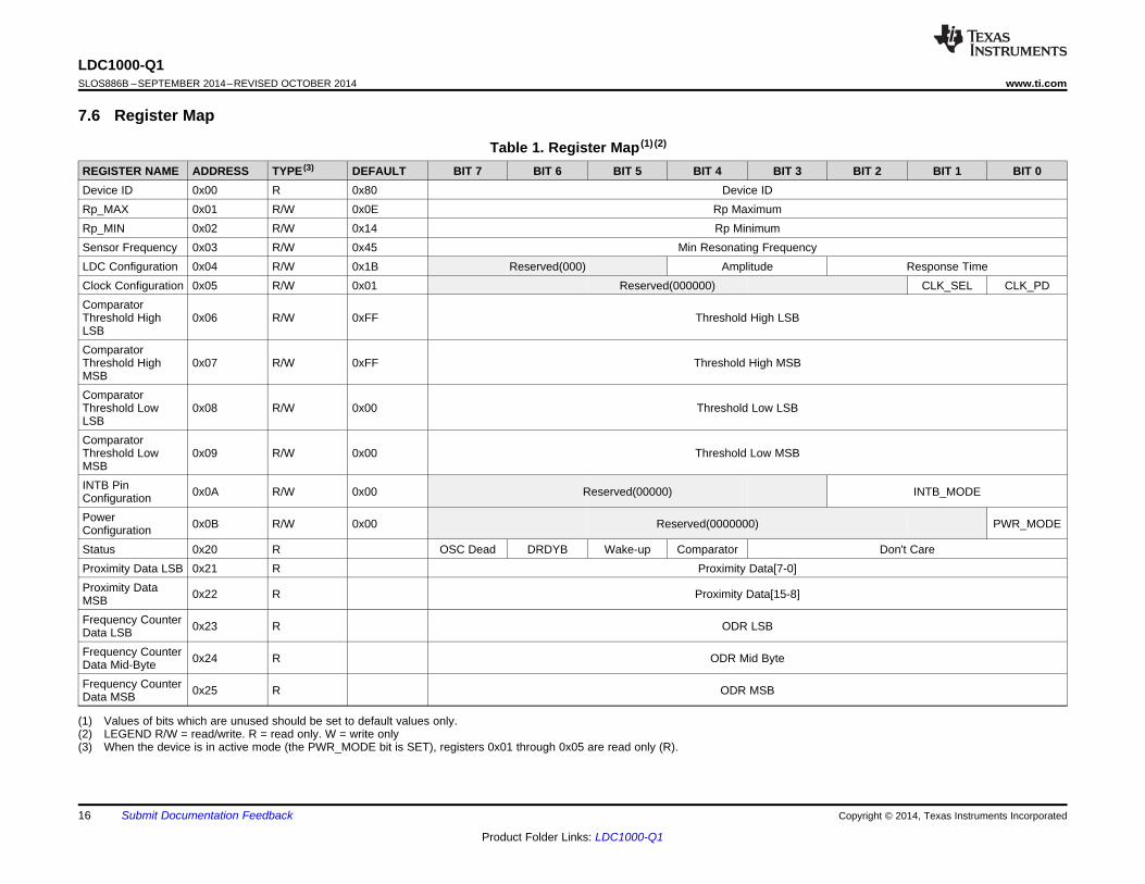
7.6 Register Map
Table 1. Register Map (1) (2)
REGISTER NAME ADDRESS TYPE (3) DEFAULT BIT 7 BIT 6 BIT 5 BIT 4 BIT 3 BIT 2 BIT 1 BIT 0Device ID 0x00 R 0x80 Device IDRp_MAX 0x01 R/W 0x0E Rp MaximumRp_MIN 0x02 R/W 0x14 Rp MinimumSensor Frequency 0x03 R/W 0x45 Min Resonating FrequencyLDC Configuration 0x04 R/W 0x1B Reserved(000) Amplitude Response TimeClock Configuration 0x05 R/W 0x01 Reserved(000000) CLK_SEL CLK_PDComparatorThreshold High 0x06 R/W 0xFF Threshold High LSBLSBComparatorThreshold High 0x07 R/W 0xFF Threshold High MSBMSBComparatorThreshold Low 0x08 R/W 0x00 Threshold Low LSBLSBComparatorThreshold Low 0x09 R/W 0x00 Threshold Low MSBMSBINTB Pin 0x0A R/W 0x00 Reserved(00000) INTB_MODEConfigurationPower 0x0B R/W 0x00 Reserved(0000000) PWR_MODEConfigurationStatus 0x20 R OSC Dead DRDYB Wake-up Comparator Don't CareProximity Data LSB 0x21 R Proximity Data[7-0]Proximity Data 0x22 R Proximity Data[15-8]MSBFrequency Counter 0x23 R ODR LSBData LSBFrequency Counter 0x24 R ODR Mid ByteData Mid-ByteFrequency Counter 0x25 R ODR MSBData MSB
(1) Values of bits which are unused should be set to default values only.(2) LEGEND R/W = read/write. R = read only. W = write only(3) When the device is in active mode (the PWR_MODE bit is SET), registers 0x01 through 0x05 are read only (R).
16 Submit Documentation Feedback Copyright © 2014, Texas Instruments Incorporated
Product Folder Links: LDC1000-Q1

LDC1000-Q1www.ti.com SLOS886B –SEPTEMBER 2014–REVISED OCTOBER 2014
7.6.1 Register Description
7.6.1.1 Revision ID (offset = 0x00) [reset = 0x80]
Figure 17. Revision ID Register
7 6 5 4 3 2 1 0Revision ID
RLEGEND: R/W = Read/Write; R = Read only; -n = value after reset
Table 2. Revision ID Field DescriptionsBit Field Type Reset Description7-0 Revision ID R 0x080 Revision ID of silicon.
Copyright © 2014, Texas Instruments Incorporated Submit Documentation Feedback 17
Product Folder Links: LDC1000-Q1

LDC1000-Q1SLOS886B –SEPTEMBER 2014–REVISED OCTOBER 2014 www.ti.com
7.6.1.2 Rp_MAX (offset = 0x01) [reset = 0x0E]
Figure 18. Rp_MAX Register
7 6 5 4 3 2 1 0Rp Maximum
R/WLEGEND: R/W = Read/Write; R = Read only; -n = value after reset
Table 3. Rp_MAX Field DescriptionsBit Field Type Reset Description7-0 Rp Maximum R/W 0x0E Maximum RP that the LDC1000-Q1 device must measure.
Configures the input dynamic range of the LDC1000-Q1 device.Register setting for Rp_MAX (kΩ):
0x00 = 3926.991
0x01 = 3141.593
0x02 = 2243.995
0x03 = 1745.329
0x04 = 1308.997
0x05 = 981.748
0x06 = 747.998
0x07 = 581.776
0x08 = 436.332
0x09 = 349.066
0x0A = 249.333
0x0B = 193.926
0x0C = 145.444
0x0D = 109.083
0x0E = 83.111
0x0F = 64.642
0x10 = 48.481
0x11 = 38.785
0x12 = 27.704
0x13 = 21.547
0x14 = 16.16
0x15 = 12.12
0x16 = 9.235
0x17 = 7.182
0x18 = 5.387
0x19 = 4.309
0x1A = 3.078
0x1B = 2.394
0x1C = 1.796
0x1D = 1.347
0x1E = 1.026
0x1F = 0.798
18 Submit Documentation Feedback Copyright © 2014, Texas Instruments Incorporated
Product Folder Links: LDC1000-Q1

LDC1000-Q1www.ti.com SLOS886B –SEPTEMBER 2014–REVISED OCTOBER 2014
7.6.1.3 Rp_MIN (offset = 0x02) [reset = 0x14]
Figure 19. Rp_MIN Register
7 6 5 4 3 2 1 0Rp Minimum
R/WLEGEND: R/W = Read/Write; R = Read only; -n = value after reset
Table 4. Rp_MIN Field DescriptionsBit Field Type Reset Description7-0 Rp Minimum R/W 0x014 Minimum RP that the LDC1000-Q1 device must measure.
Configures the input dynamic range of the LDC1000-Q1 device.Register setting for Rp_MIN (kΩ):
0x20 = 3926.991
0x21 = 3141.593
0x22 = 2243.995
0x23 = 1745.329
0x24 = 1308.997
0x25 = 981.748
0x26 = 747.998
0x27 = 581.776
0x28 = 436.332
0x29 = 349.066
0x2A = 249.333
0x2B = 193.926
0x2C = 145.444
0x2D = 109.083
0x2E = 83.111
0x2F = 64.642
0x30 = 48.481
0x31 = 38.785
0x32 = 27.704
0x33 = 21.547
0x34 = 16.16
0x35 = 12.12
0x36 = 9.235
0x37 = 7.182
0x38 = 5.387
0x39 = 4.309
0x3A = 3.078
0x3B = 2.394
0x3C = 1.796
0x3D = 1.347
0x3E = 1.026
0x3F = 0.798
Copyright © 2014, Texas Instruments Incorporated Submit Documentation Feedback 19
Product Folder Links: LDC1000-Q1

LDC1000-Q1SLOS886B –SEPTEMBER 2014–REVISED OCTOBER 2014 www.ti.com
7.6.1.4 Sensor Frequency (offset = 0x03) [reset = 0x45]
Figure 20. Sensor Frequency Register
7 6 5 4 3 2 1 0Min Resonating Frequency
R/WLEGEND: R/W = Read/Write; R = Read only; -n = value after reset
Table 5. Sensor Frequency Field DescriptionsBit Field Type Reset Description7-0 Min Resonating Frequency R/W 0x45 Sets the minimum resonating frequency to approximately 20%
below the lowest resonating frequency of the sensor with notarget in front. Use the formula below to determine the value ofregister.
N = 68.94 × log10(f / 2000)
where• N = Register Value. Round to nearest
value.• f = 20% below resonating frequency,
Hz (11)Example: Sensor frequency (fsensor) = 1 MHz
f = 0.8 × 1 MHz = 800 KHz (12)N = 68.94 × log10(800 KHz / 2000) = Round to nearestwhole number (179.38) = 179 (Value to be programmedin the sensor frequency register) (13)
7.6.1.5 LDC Configuration (offset = 0x04) [reset = 0x1B]
Figure 21. LDC Configuration Register
7 6 5 4 3 2 1 0Reserved Amplitude Response Time
— R/W R/WLEGEND: R/W = Read/Write; R = Read only; -n = value after reset
Table 6. LDC Configuration Field DescriptionsBit Field Type Reset Description7-5 Reserved — — Reserved to 04-3 Amplitude R/W 0x1B Sets the oscillation amplitude
00: 1 V
01: 2 V
10: 4 V
11: Reserved2-0 Response Time R/W 0x1B Sets the response time
000: Reserved
001: Reserved
010: 192
011: 384
100: 768
101: 1536
110: 3072
111: 6144
20 Submit Documentation Feedback Copyright © 2014, Texas Instruments Incorporated
Product Folder Links: LDC1000-Q1

LDC1000-Q1www.ti.com SLOS886B –SEPTEMBER 2014–REVISED OCTOBER 2014
7.6.1.6 Clock Configuration (offset = 0x05) [reset = 0x01]
Figure 22. Clock Configuration Register
7 6 5 4 3 2 1 0Reserved CLK_SEL CLK_PD
R/W R/W R/WLEGEND: R/W = Read/Write; R = Read only; -n = value after reset
Table 7. Clock Configuration Field DescriptionsBit Field Type Reset Description7-2 Resrved — — Reserved to 01 CLK_SEL R/W 0x01 1:External crystal used for frequency counter (XIN or
XOUT).
0:External time-base clock used for frequency counter(TBCLK).
0 CLK_PD R/W 0x01 1:Disable external time base clock. Crystal oscillatorpower down.0:Enable External time base clock.
7.6.1.7 Comparator Threshold High LSB (offset = 0x06) [reset = 0xFF]
Figure 23. Comparator Threshold High LSB Register
7 6 5 4 3 2 1 0Threshold Threshold Threshold Threshold Threshold Threshold Threshold ThresholdHigh[7:0] High[6] High[5] High[4] High[3] High[2] High[1] High[0]
R/W R/W R/W R/W R/W R/W R/W R/WLEGEND: R/W = Read/Write; R = Read only; -n = value after reset
Table 8. Comparator Threshold High LSB Field DescriptionsBit Field Type Reset Description7:0 Threshold High LSB R/W 0xFF Least Significant byte (LSB) of the threshold high register. This
Threshold High[7:0] register is a buffer. A read reflects the current value of thethreshold high[7:0] register. See the Comparator Threshold HighMSB (offset = 0x07) [reset = 0xFF] section for details onupdating the threshold high register.
7.6.1.8 Comparator Threshold High MSB (offset = 0x07) [reset = 0xFF]
Figure 24. Comparator Threshold High MSB Register
7 6 5 4 3 2 1 0Threshold Threshold Threshold Threshold Threshold Threshold Threshold ThresholdHigh[15] High[14] High[13] High[12] High[11] High[10] High[9] High[8]
R/W R/W R/W R/W R/W R/W R/W R/WLEGEND: R/W = Read/Write; R = Read only; -n = value after reset
Table 9. Comparator Threshold High MSB Field DescriptionsBit Field Type Reset Description7:0 Threshold High MSB R/W 0xFF Most significant byte (MSB) of the threshold high register. A
Threshold High[15:8] write to this register copies the contents of the 0x06 register andwrites to the threshold high register[15:0]. A read returns thethreshold high [15:8] register. To update the threshold highregister write register 0x06 first and then 0x07.
Copyright © 2014, Texas Instruments Incorporated Submit Documentation Feedback 21
Product Folder Links: LDC1000-Q1

LDC1000-Q1SLOS886B –SEPTEMBER 2014–REVISED OCTOBER 2014 www.ti.com
7.6.1.9 Comparator Threshold Low LSB (offset = 0x08) [reset = 0x00]
Figure 25. Comparator Threshold Low LSB Register
7 6 5 4 3 2 1 0Threshold Threshold Threshold Threshold Threshold Threshold Threshold ThresholdLow[7:0] Low[6] Low[5] Low[4] Low[3] Low[2] Low[1] Low[0]
R/W R/W R/W R/W R/W R/W R/W R/WLEGEND: R/W = Read/Write; R = Read only; -n = value after reset
Table 10. Comparator Threshold Low LSB Field DescriptionsBit Field Type Reset Description7:0 Threshold Low LSB R/W 0x00 Least significant byte of the threshold low value. This register is
Threshold Low[7:0] a buffer. A read reflects the current value of the threshold low[7:0] register. See the Comparator Threshold Low MSB (offset =0x09) [reset = 0x00] section for details on updating the thresholdlow register.
7.6.1.10 Comparator Threshold Low MSB (offset = 0x09) [reset = 0x00]
Figure 26. Comparator Threshold Low MSB Register
7 6 5 4 3 2 1 0Threshold Threshold Threshold Threshold Threshold Threshold Threshold ThresholdLow[15] Low[14] Low[13] Low[12] Low[11] Low[10] Low[9] Low[8]
R/W R/W R/W R/W R/W R/W R/W R/WLEGEND: R/W = Read/Write; R = Read only; -n = value after reset
Table 11. Comparator Threshold Low MSB Field DescriptionsBit Field Type Reset Description7:0 Threshold Low MSB R/W 0x00 Most significant byte of the threshold low register. A write to this
Threshold Low[15:8] register copies the contents of the 0x08 register and writes tothe threshold low register[15:0]. A read returns the threshold low[15:8] register. To update the threshold low register write registeraddress 0x08 first and then 0x09.
7.6.1.11 INTB Pin Configuration (offset = 0x0A) [reset = 0x00]
Figure 27. INTB Pin Configuration Register
7 6 5 4 3 2 1 0Reserved Mode
— R/WLEGEND: R/W = Read/Write; R = Read only; -n = value after reset
Table 12. INTB Pin Configuration Field DescriptionsBit Field Type Reset Description7:3 Reserved — — Reserved to 02:0 Mode R/W 0x00 100: DRDYB enabled on the INTB pin
010: The INTB pin indicates the status of the comparator output001: Wake-up enabled on the INTB pin000: All modes disabledAll other combinations are reserved
22 Submit Documentation Feedback Copyright © 2014, Texas Instruments Incorporated
Product Folder Links: LDC1000-Q1

LDC1000-Q1www.ti.com SLOS886B –SEPTEMBER 2014–REVISED OCTOBER 2014
7.6.1.12 Power Configuration (offset = 0x0B) [reset = 0x00]
Figure 28. Power Configuration Register
7 6 5 4 3 2 1 0Reserved PWR_MODE
— R/WLEGEND: R/W = Read/Write; R = Read only; -n = value after reset
Table 13. Power Configuration Field DescriptionsBit Field Type Reset Description7:1 Reserved — — Reserved to 00 PWR_MODE R/W 0x00 0: Stand-by mode
1: Active mode. Conversion is enabled
7.6.1.13 Status (offset = 0x20) [reset = NA]
Figure 29. Status Register
7 6 5 4 3 2 1 0OSC status Data Ready Wake-up Comparator Don't Care
R R R R RLEGEND: R/W = Read/Write; R = Read only; -n = value after reset
Table 14. Status Field DescriptionsBit Field Type Reset Description7 OSC status R NA 1: Indicates that the oscillator is overloaded and has stopped
0: Oscillator is working6 Data Ready R NA 0: Data is ready to be read
1: No new data is available5 Wake-up R NA 0: Wake-up triggered. Proximity data is more than the threshold
high value.1: Wake-up is disabled
4 Comparator R NA 0: Proximity data is more than the threshold high value1: Proximity data is less than the threshold low value
3:0 Don't Care R NA
7.6.1.14 Proximity Data LSB (offset = 0x21) [reset = NA]
Figure 30. Proximity Data LSB Register
7 6 5 4 3 2 1 0Proximity Proximity Proximity Proximity Proximity Proximity Proximity ProximityData[7] Data[6] Data[5] Data[4] Data[3] Data[2] Data[1] Data[0]
R R R R R R R RLEGEND: R/W = Read/Write; R = Read only; -n = value after reset
Table 15. Proximity Data LSB Field DescriptionsBit Field Type Reset Description7:0 Proximity Data[7:0] R NA Least significant byte of proximity data
Copyright © 2014, Texas Instruments Incorporated Submit Documentation Feedback 23
Product Folder Links: LDC1000-Q1

LDC1000-Q1SLOS886B –SEPTEMBER 2014–REVISED OCTOBER 2014 www.ti.com
7.6.1.15 Proximity Data MSB (offset = 0x22) [reset = NA]
Figure 31. Proximity Data MSB Register
7 6 5 4 3 2 1 0Proximity Proximity Proximity Proximity Proximity Proximity Proximity ProximityData[15] Data[14] Data[13] Data[12] Data[11] Data[10] Data[9] Data[8]
R R R R R R R RLEGEND: R/W = Read/Write; R = Read only; -n = value after reset
Table 16. Proximity Data MSB Field DescriptionsBit Field Type Reset Description7:0 Proximity data[15:8] R NA Most significant byte of proximity data
7.6.1.16 Frequency Counter LSB (offset = 0x23) [reset = NA]
Figure 32. Frequency Counter LSB Register
7 6 5 4 3 2 1 0ODR[7] ODR[6] ODR[5] ODR[4] ODR[3] ODR[2] ODR[1] ODR[0]
R R R R R R R RLEGEND: R/W = Read/Write; R = Read only; -n = value after reset
Table 17. Frequency Counter LSB Field DescriptionsBit Field Type Reset Description7:0 ODR LSB R NA LSB of output data rate. Sensor frequency can be calculated
ODR[7:0] using the output data rate. See the Measuring Inductancesection.
7.6.1.17 Frequency Counter Mid-Byte (offset = 0x24) [reset = NA]
Figure 33. Frequency Counter Mid-Byte Register
7 6 5 4 3 2 1 0ODR[15] ODR[14] ODR[13] ODR[12] ODR[11] ODR[10] ODR[9] ODR[8]
R R R R R R R RLEGEND: R/W = Read/Write; R = Read only; -n = value after reset
Table 18. Frequency Counter Mid-Byte Field DescriptionsBit Field Type Reset Description7:0 ODR Mid byte R NA Middle byte of output data rate
ODR[15:8]
24 Submit Documentation Feedback Copyright © 2014, Texas Instruments Incorporated
Product Folder Links: LDC1000-Q1

LDC1000-Q1www.ti.com SLOS886B –SEPTEMBER 2014–REVISED OCTOBER 2014
7.6.1.18 Frequency Counter MSB (offset = 0x25) [reset = NA]
Figure 34. Frequency Counter MSB Register
7 6 5 4 3 2 1 0ODR[23] ODR[22] ODR[21] ODR[20] ODR[19] ODR[18] ODR[17] ODR[16]
R R R R R R R RLEGEND: R/W = Read/Write; R = Read only; -n = value after reset
Table 19. Frequency Counter MSB Field Descriptions (1)
Bit Field Type Reset Description7:0 ODR MSB R NA MSB of Output data rate
ODR[23:16]
(1) Care must be taken to ensure that the proximity data[15:0] and Frequency Counter[23:0] registers are all from same conversion.Conversion data is updated to these registers only when a read is initiated on 0x21 register. If the read is delayed between subsequentconversions, these registers are not updated until another read is initiated on 0x21.
Copyright © 2014, Texas Instruments Incorporated Submit Documentation Feedback 25
Product Folder Links: LDC1000-Q1

LDC1000-Q1SLOS886B –SEPTEMBER 2014–REVISED OCTOBER 2014 www.ti.com
8 Application and Implementation
NOTEInformation in the following applications sections is not part of the TI componentspecification, and TI does not warrant its accuracy or completeness. TI’s customers areresponsible for determining suitability of components for their purposes. Customers shouldvalidate and test their design implementation to confirm system functionality.
8.1 Application Information
8.1.1 Calculation of Rp_Min and Rp_MaxDifferent sensing applications may have a different ranges of the resonance impedance RP to measure. TheLDC1000-Q1 measurement range of RP is controlled by setting two registers: Rp_MIN and Rp_MAX. For a givenapplication, RP must never be outside the range set by these register values, otherwise the measured value willbe clipped. For optimal sensor resolution, the range of Rp_MIN to Rp_MAX should not be unnecessarily large.The following procedure is recommended to determine the Rp_MIN and Rp_MAX register values.
8.1.1.1 Rp_MAXRp_MAX sets the upper limit of the LDC1000-Q1 resonant impedance input range.
• Configure the sensor such that the eddy-current losses are minimized. As an example, for a proximity sensingapplication, set the distance between the sensor and the target to the maximum sensing distance.
• Measure the resonant impedance RP using an impedance analyzer.• Multiply RP by 2 and use the next higher value from the register settings listed in Table 3.
For example, if RP is measured at 18 kΩ, 18000 × 2 = 36000. Referring to Table 3, 38.785 kΩ is the smallestvalue larger than 36 kΩ; therefore Rp_MAX should be set to 0x11.
Setting Rp_MAX to a value not listed in Table 3 can result in indeterminate behavior.
8.1.1.2 Rp_MINRp_MIN sets the lower limit of the LDC1000-Q1 resonant impedance input range.
• Configure the sensor such that the eddy current losses are maximized. As an example, for a proximitysensing application, set the distance between the sensor and the metal target to the minimum sensingdistance.
• Measure the resonant impedance RP using an impedance analyzer.• Divide the RP value by 2 and then select the next lower RP value from the register settings listed in Table 4.
For example, if RP at 1 mm is measured to be 5 kΩ, 5000 / 2 = 2500. Referring to Table 4, 2.394 kΩ is thesmallest value smaller than 2.5 kΩ which corresponds to an Rp_MIN value of 0x3B.
Setting Rp_MIN to a value not listed on Table 4 can result in indeterminate behavior. In addition, Rp_MIN powerson with a default value of 0x14 which must be set to a value from Table 4 prior to powering on the LDC.
8.1.2 Output Data RateThe output data rate of the LDC1000-Q1 device depends on the sensor frequency, fsensor and the ResponseTime[2-0] field in the LDC configuration register (address: 0x04).
Output data rate = fsensor / (Response Time[2-0] / 3) in SPS (samples per second) (14)
8.1.2.1 ExampleIf the following values are selected, fsensor= 5 Mhz and Response Time[2-0] = 192, then:
Output data rate = 5 MHz / (192 / 3) = 78.125 KSPS (15)
26 Submit Documentation Feedback Copyright © 2014, Texas Instruments Incorporated
Product Folder Links: LDC1000-Q1

LDC1000-Q1www.ti.com SLOS886B –SEPTEMBER 2014–REVISED OCTOBER 2014
Application Information (continued)8.1.3 Selecting a Filter Capacitor (CFA and CFB Pins)The filter capacitor is critical to the operation of the LDC1000-Q1 device. The capacitor should be low leakage,temperature stable, and it must not generate any piezoelectric noise (the dielectrics of many capacitors exhibitpiezoelectric characteristics and any such noise is coupled directly through RP into the converter). The optimalcapacitance values range from 20 pF to 100 nF. The value of the capacitor is based on the time constant andresonating frequency of the LC tank.
If a ceramic capacitor is used, then a C0G (or NP0) grade dielectric is recommended. The voltage rating shouldbe 10 V or higher. The traces connecting the CFA and CFB pins to the capacitor should be as short as possibleto minimize any parasitics.
For optimal performance, the selected filter capacitor, connected between the CFA and CFB pins, must be assmall as possible but large enough such that the active filter does not saturate. The size of this capacitordepends on the time constant of the sense coil, which is given by L / rs (L = inductance, rs = series resistance ofthe inductor at oscillation frequency). The larger this time constant, the larger filter capacitor is required.Therefore the time constant reaches the maximum when there is no target present in front of the sensing coil.
Use the following procedure to find the optimal filter capacitance:1. Use with a large filter capacitor. For a ferrite core coil, a value of 10 nF is generally large enough. For an air
coil or PCB coil, a value of 100 pF is generally large enough.2. Power on the LDC and set the desired register values.3. Minimize the eddy currents losses by ensuring maximum clearance between the target and the sensing coil.4. Observe the signal on the CFB pin using a scope. Because this node is very sensitive to capacitive loading,
the use of an active probe is recommended. As an alternative, a passive probe with a 1-kΩ series resistancebetween the tip and the CFB pin can be used.
5. Vary the values of the filter capacitor until the signal observed on the CFB pin has an amplitude ofapproximately 1 VPP. This signal scales linearly with the reciprocal of the filter capacitance. For example, if a100-pF filter capacitor is applied and the signal observed on the CFB pin has a peak-to-peak value of 200mV, the desired 1-VPP value is obtained using a filter capacitor value that is calculated with Equation 16.
200 mV / 1 V × 100 pF = 20 pF (16)
Copyright © 2014, Texas Instruments Incorporated Submit Documentation Feedback 27
Product Folder Links: LDC1000-Q1

(Rp
)
MCU
LDO
LDC1000
5 V
5 V
DGND
DGND
AGND
Sensor
VIO
DGND
VIO VDD
VIO
CLDO
SDI
SDO
SCLK
CSB
INTB
TBCLK
DGND
MOSI
MISO
SCLK
GPIO
INT/GPIO
Timer/Aux CLK
DAP
GND
CFB
CFA
INB
INA
LDC1000-Q1SLOS886B –SEPTEMBER 2014–REVISED OCTOBER 2014 www.ti.com
8.2 Typical Application
Figure 35. Typical Application Schematic
Figure 36. Linear Position Sensing
28 Submit Documentation Feedback Copyright © 2014, Texas Instruments Incorporated
Product Folder Links: LDC1000-Q1

(Rp
)
LDC1000-Q1www.ti.com SLOS886B –SEPTEMBER 2014–REVISED OCTOBER 2014
Typical Application (continued)
Figure 37. Angular Position Sensing
8.2.1 Design RequirementsFor this design example, use the following as the input parameters.
Table 20. Design ParametersDESIGN PARAMETER EXAMPLE VALUE
Minimum sensing distance 1 mmMaximum sensing distance 8 mm
Output data rate 78 KSPS (Max data rate with LDC10xx series)Number of PCB layers for sensor 2 layers
8.2.2 Detailed Design Procedure
8.2.2.1 Sensor and TargetIn this example, consider a sensor with the characteristics listed in Table 21.
Table 21. Sensor CharacteristicsPARAMETER VALUE
Layers 2Thickness of copper 1 oz
Coil shape CircularNumber of turns 23Trace thickness 4 milTrace spacing 4 mil
PCB core material FR4RP at 1 mm 5 kΩRP at 8 mm 12.5 kΩ
Nominal Inductance 18 µH
Copyright © 2014, Texas Instruments Incorporated Submit Documentation Feedback 29
Product Folder Links: LDC1000-Q1

10F
N 68.94 log2500
§ · u ¨ ¸
© ¹
2sensor
1L
C (2 f )
u Su
sensorfOutput Data Rate
Response time3
§ ·¨ ¸© ¹
LDC1000-Q1SLOS886B –SEPTEMBER 2014–REVISED OCTOBER 2014 www.ti.com
The target material used is stainless steel.
8.2.2.2 Calculating a Sensor CapacitorSensor frequency depends on various factors in the application. In this example, use Equation 17 to calculate thesensor frequency in order to achieve an output data rate of 78 KSPS per the design parameter.
(17)
With the lowest response time (tres) of 192 and output data rate of 78 KSPS, the calculated sensor frequencyusing Equation 17 is 4.99 MHz.
Use Equation 18 to calculate the sensor capacitor as 55 pF with a sensor inductance of 18 µH.
(18)
8.2.2.3 Selecting a Filter CapacitorUse the steps listed in the Selecting a Filter Capacitor (CFA and CFB Pins) section to calculate a filter capacitor.For this example, the selected capacitor value is 20 pF. The following waveforms were taken on the CFB pin witha 14-mm, 2-layer PCB coil (23 turns, 4-mil trace width, 4-mil spacing between trace, 1-o.z copper thickness,FR4).
Figure 38. Waveform on CFB With 100 pF Figure 39. Waveform on CFB With 20 pF
8.2.2.4 Setting Rp_MIN and Rp_MAXTo calculate the value for the Rp_MAX register, use the following value: Rp at 8 mm is 12.5 kΩ, 12500 × 2 =25000. Then 27.704 kΩ is the nearest value larger than 25 kΩ. Referring to Table 3, this value corresponds to aRp_MAX value of 0x12.
To calculate the value for the Rp_MAX register, use the following value: Rp at 1 mm is 5 kΩ, 5000 / 2 = 2500.Then 2.394 kΩ is the nearest value lower than 2.5 kΩ. Referring to Table 4, this value corresponds to Rp_MINvalue of 0x3B.
8.2.2.5 Calculating Minimum Sensor FrequencyUse Equation 19 to calculate the minimum sensor frequency.
where• N is 227.51 (19)
30 Submit Documentation Feedback Copyright © 2014, Texas Instruments Incorporated
Product Folder Links: LDC1000-Q1

0
2
4
6
8
10
12
14
0 1 2 3 4 5 6 7 8
Rp
(k
Distance (mm) C002
0
5
10
15
20
25
0 1 2 3 4 5 6 7 8
Indu
ctan
ce (
µH
)
Distance (mm) C001
LDC1000-Q1www.ti.com SLOS886B –SEPTEMBER 2014–REVISED OCTOBER 2014
For this example, round the value of N up to 228. This value must be written into the watchdog timer register,which is used to wake up the internal circuit when the sensor is saturated.
8.2.3 Application Curves
Figure 41. Inductance vs DistanceFigure 40. RP vs Distance
Copyright © 2014, Texas Instruments Incorporated Submit Documentation Feedback 31
Product Folder Links: LDC1000-Q1

LDC1000-Q1SLOS886B –SEPTEMBER 2014–REVISED OCTOBER 2014 www.ti.com
9 Power Supply RecommendationsThe LDC1000-Q1 device is designed to operate from an analog supply range of 4.75 to 5.25 V and digital I/Osupply range of 1.8 to 5.25 V. The analog supply voltage should be greater than or equal to the digital supplyvoltage for proper operation of the device. The supply voltage should be well regulated. If the supply is locatedmore than a few inches from the LDC1000-Q1 device, additional bulk capacitance may be required in addition tothe ceramic bypass capacitors.
10 Layout
10.1 Layout GuidelinesUse the following guidelines:• Bypass the VDD and VIO pin to ground with a low ESR ceramic bypass capacitor. A ceramic X7R dielectric
capacitor with a value of 0.1 µF is recommend.• Place the VDD, VIO, GND, and DGND pins as close to the device as possible. Take care to minimize the
loop area formed by the bypass capacitor connection and the VDD, VIO, GND, and DGND pins of the IC. SeeFigure 42 for a PCB layout example.
• Bypass the CLDO pin to the digital ground (DGND) with a ceramic bypass capacitor with a value of 56 nF.• Connect the filter capacitor that is selected using the procedure listed in the Selecting a Filter Capacitor (CFA
and CFB Pins) section between the CFA and CFB pins. Place the capacitor close to the CFA and CFB pins.Do not use any ground or power planes below the capacitor and the trace connecting the capacitor and theCFx pins.
• Use two separate ground planes for the ground (GND) and digital ground (DGND) for a star connection asrecommended. See Figure 42 for a PCB layout example.
32 Submit Documentation Feedback Copyright © 2014, Texas Instruments Incorporated
Product Folder Links: LDC1000-Q1

LDC1000-Q1www.ti.com SLOS886B –SEPTEMBER 2014–REVISED OCTOBER 2014
10.2 Layout Example
Figure 42. LDC10xx Board Layout
Copyright © 2014, Texas Instruments Incorporated Submit Documentation Feedback 33
Product Folder Links: LDC1000-Q1

LDC1000-Q1SLOS886B –SEPTEMBER 2014–REVISED OCTOBER 2014 www.ti.com
11 Device and Documentation Support
11.1 TrademarksAll trademarks are the property of their respective owners.
11.2 Electrostatic Discharge CautionThese devices have limited built-in ESD protection. The leads should be shorted together or the device placed in conductive foamduring storage or handling to prevent electrostatic damage to the MOS gates.
11.3 GlossarySLYZ022 — TI Glossary.
This glossary lists and explains terms, acronyms, and definitions.
12 Mechanical, Packaging, and Orderable InformationThe following pages include mechanical, packaging, and orderable information. This information is the mostcurrent data available for the designated devices. This data is subject to change without notice and revision ofthis document. For browser-based versions of this data sheet, refer to the left-hand navigation.
34 Submit Documentation Feedback Copyright © 2014, Texas Instruments Incorporated
Product Folder Links: LDC1000-Q1

PACKAGE OPTION ADDENDUM
www.ti.com 4-May-2018
Addendum-Page 1
PACKAGING INFORMATION
Orderable Device Status(1)
Package Type PackageDrawing
Pins PackageQty
Eco Plan(2)
Lead/Ball Finish(6)
MSL Peak Temp(3)
Op Temp (°C) Device Marking(4/5)
Samples
LDC1000EPWRQ1 NRND TSSOP PW 16 2500 Green (RoHS& no Sb/Br)
CU SN Level-3-260C-168 HR 0 to 0 LDC1000E
LDC1000QPWRQ1 NRND TSSOP PW 16 2500 Green (RoHS& no Sb/Br)
CU SN Level-3-260C-168 HR -40 to 125 LDC1000Q
(1) The marketing status values are defined as follows:ACTIVE: Product device recommended for new designs.LIFEBUY: TI has announced that the device will be discontinued, and a lifetime-buy period is in effect.NRND: Not recommended for new designs. Device is in production to support existing customers, but TI does not recommend using this part in a new design.PREVIEW: Device has been announced but is not in production. Samples may or may not be available.OBSOLETE: TI has discontinued the production of the device.
(2) RoHS: TI defines "RoHS" to mean semiconductor products that are compliant with the current EU RoHS requirements for all 10 RoHS substances, including the requirement that RoHS substancedo not exceed 0.1% by weight in homogeneous materials. Where designed to be soldered at high temperatures, "RoHS" products are suitable for use in specified lead-free processes. TI mayreference these types of products as "Pb-Free".RoHS Exempt: TI defines "RoHS Exempt" to mean products that contain lead but are compliant with EU RoHS pursuant to a specific EU RoHS exemption.Green: TI defines "Green" to mean the content of Chlorine (Cl) and Bromine (Br) based flame retardants meet JS709B low halogen requirements of <=1000ppm threshold. Antimony trioxide basedflame retardants must also meet the <=1000ppm threshold requirement.
(3) MSL, Peak Temp. - The Moisture Sensitivity Level rating according to the JEDEC industry standard classifications, and peak solder temperature.
(4) There may be additional marking, which relates to the logo, the lot trace code information, or the environmental category on the device.
(5) Multiple Device Markings will be inside parentheses. Only one Device Marking contained in parentheses and separated by a "~" will appear on a device. If a line is indented then it is a continuationof the previous line and the two combined represent the entire Device Marking for that device.
(6) Lead/Ball Finish - Orderable Devices may have multiple material finish options. Finish options are separated by a vertical ruled line. Lead/Ball Finish values may wrap to two lines if the finishvalue exceeds the maximum column width.
Important Information and Disclaimer:The information provided on this page represents TI's knowledge and belief as of the date that it is provided. TI bases its knowledge and belief on informationprovided by third parties, and makes no representation or warranty as to the accuracy of such information. Efforts are underway to better integrate information from third parties. TI has taken andcontinues to take reasonable steps to provide representative and accurate information but may not have conducted destructive testing or chemical analysis on incoming materials and chemicals.TI and TI suppliers consider certain information to be proprietary, and thus CAS numbers and other limited information may not be available for release.
In no event shall TI's liability arising out of such information exceed the total purchase price of the TI part(s) at issue in this document sold by TI to Customer on an annual basis.

PACKAGE OPTION ADDENDUM
www.ti.com 4-May-2018
Addendum-Page 2
OTHER QUALIFIED VERSIONS OF LDC1000-Q1 :
• Catalog: LDC1000
NOTE: Qualified Version Definitions:
• Catalog - TI's standard catalog product

TAPE AND REEL INFORMATION
*All dimensions are nominal
Device PackageType
PackageDrawing
Pins SPQ ReelDiameter
(mm)
ReelWidth
W1 (mm)
A0(mm)
B0(mm)
K0(mm)
P1(mm)
W(mm)
Pin1Quadrant
LDC1000EPWRQ1 TSSOP PW 16 2500 330.0 12.4 6.95 5.6 1.6 8.0 12.0 Q1
LDC1000QPWRQ1 TSSOP PW 16 2500 330.0 12.4 6.95 5.6 1.6 8.0 12.0 Q1
PACKAGE MATERIALS INFORMATION
www.ti.com 12-Feb-2017
Pack Materials-Page 1

*All dimensions are nominal
Device Package Type Package Drawing Pins SPQ Length (mm) Width (mm) Height (mm)
LDC1000EPWRQ1 TSSOP PW 16 2500 367.0 367.0 35.0
LDC1000QPWRQ1 TSSOP PW 16 2500 367.0 367.0 35.0
PACKAGE MATERIALS INFORMATION
www.ti.com 12-Feb-2017
Pack Materials-Page 2


IMPORTANT NOTICE
Texas Instruments Incorporated (TI) reserves the right to make corrections, enhancements, improvements and other changes to itssemiconductor products and services per JESD46, latest issue, and to discontinue any product or service per JESD48, latest issue. Buyersshould obtain the latest relevant information before placing orders and should verify that such information is current and complete.TI’s published terms of sale for semiconductor products (http://www.ti.com/sc/docs/stdterms.htm) apply to the sale of packaged integratedcircuit products that TI has qualified and released to market. Additional terms may apply to the use or sale of other types of TI products andservices.Reproduction of significant portions of TI information in TI data sheets is permissible only if reproduction is without alteration and isaccompanied by all associated warranties, conditions, limitations, and notices. TI is not responsible or liable for such reproduceddocumentation. Information of third parties may be subject to additional restrictions. Resale of TI products or services with statementsdifferent from or beyond the parameters stated by TI for that product or service voids all express and any implied warranties for theassociated TI product or service and is an unfair and deceptive business practice. TI is not responsible or liable for any such statements.Buyers and others who are developing systems that incorporate TI products (collectively, “Designers”) understand and agree that Designersremain responsible for using their independent analysis, evaluation and judgment in designing their applications and that Designers havefull and exclusive responsibility to assure the safety of Designers' applications and compliance of their applications (and of all TI productsused in or for Designers’ applications) with all applicable regulations, laws and other applicable requirements. Designer represents that, withrespect to their applications, Designer has all the necessary expertise to create and implement safeguards that (1) anticipate dangerousconsequences of failures, (2) monitor failures and their consequences, and (3) lessen the likelihood of failures that might cause harm andtake appropriate actions. Designer agrees that prior to using or distributing any applications that include TI products, Designer willthoroughly test such applications and the functionality of such TI products as used in such applications.TI’s provision of technical, application or other design advice, quality characterization, reliability data or other services or information,including, but not limited to, reference designs and materials relating to evaluation modules, (collectively, “TI Resources”) are intended toassist designers who are developing applications that incorporate TI products; by downloading, accessing or using TI Resources in anyway, Designer (individually or, if Designer is acting on behalf of a company, Designer’s company) agrees to use any particular TI Resourcesolely for this purpose and subject to the terms of this Notice.TI’s provision of TI Resources does not expand or otherwise alter TI’s applicable published warranties or warranty disclaimers for TIproducts, and no additional obligations or liabilities arise from TI providing such TI Resources. TI reserves the right to make corrections,enhancements, improvements and other changes to its TI Resources. TI has not conducted any testing other than that specificallydescribed in the published documentation for a particular TI Resource.Designer is authorized to use, copy and modify any individual TI Resource only in connection with the development of applications thatinclude the TI product(s) identified in such TI Resource. NO OTHER LICENSE, EXPRESS OR IMPLIED, BY ESTOPPEL OR OTHERWISETO ANY OTHER TI INTELLECTUAL PROPERTY RIGHT, AND NO LICENSE TO ANY TECHNOLOGY OR INTELLECTUAL PROPERTYRIGHT OF TI OR ANY THIRD PARTY IS GRANTED HEREIN, including but not limited to any patent right, copyright, mask work right, orother intellectual property right relating to any combination, machine, or process in which TI products or services are used. Informationregarding or referencing third-party products or services does not constitute a license to use such products or services, or a warranty orendorsement thereof. Use of TI Resources may require a license from a third party under the patents or other intellectual property of thethird party, or a license from TI under the patents or other intellectual property of TI.TI RESOURCES ARE PROVIDED “AS IS” AND WITH ALL FAULTS. TI DISCLAIMS ALL OTHER WARRANTIES ORREPRESENTATIONS, EXPRESS OR IMPLIED, REGARDING RESOURCES OR USE THEREOF, INCLUDING BUT NOT LIMITED TOACCURACY OR COMPLETENESS, TITLE, ANY EPIDEMIC FAILURE WARRANTY AND ANY IMPLIED WARRANTIES OFMERCHANTABILITY, FITNESS FOR A PARTICULAR PURPOSE, AND NON-INFRINGEMENT OF ANY THIRD PARTY INTELLECTUALPROPERTY RIGHTS. TI SHALL NOT BE LIABLE FOR AND SHALL NOT DEFEND OR INDEMNIFY DESIGNER AGAINST ANY CLAIM,INCLUDING BUT NOT LIMITED TO ANY INFRINGEMENT CLAIM THAT RELATES TO OR IS BASED ON ANY COMBINATION OFPRODUCTS EVEN IF DESCRIBED IN TI RESOURCES OR OTHERWISE. IN NO EVENT SHALL TI BE LIABLE FOR ANY ACTUAL,DIRECT, SPECIAL, COLLATERAL, INDIRECT, PUNITIVE, INCIDENTAL, CONSEQUENTIAL OR EXEMPLARY DAMAGES INCONNECTION WITH OR ARISING OUT OF TI RESOURCES OR USE THEREOF, AND REGARDLESS OF WHETHER TI HAS BEENADVISED OF THE POSSIBILITY OF SUCH DAMAGES.Unless TI has explicitly designated an individual product as meeting the requirements of a particular industry standard (e.g., ISO/TS 16949and ISO 26262), TI is not responsible for any failure to meet such industry standard requirements.Where TI specifically promotes products as facilitating functional safety or as compliant with industry functional safety standards, suchproducts are intended to help enable customers to design and create their own applications that meet applicable functional safety standardsand requirements. Using products in an application does not by itself establish any safety features in the application. Designers mustensure compliance with safety-related requirements and standards applicable to their applications. Designer may not use any TI products inlife-critical medical equipment unless authorized officers of the parties have executed a special contract specifically governing such use.Life-critical medical equipment is medical equipment where failure of such equipment would cause serious bodily injury or death (e.g., lifesupport, pacemakers, defibrillators, heart pumps, neurostimulators, and implantables). Such equipment includes, without limitation, allmedical devices identified by the U.S. Food and Drug Administration as Class III devices and equivalent classifications outside the U.S.TI may expressly designate certain products as completing a particular qualification (e.g., Q100, Military Grade, or Enhanced Product).Designers agree that it has the necessary expertise to select the product with the appropriate qualification designation for their applicationsand that proper product selection is at Designers’ own risk. Designers are solely responsible for compliance with all legal and regulatoryrequirements in connection with such selection.Designer will fully indemnify TI and its representatives against any damages, costs, losses, and/or liabilities arising out of Designer’s non-compliance with the terms and provisions of this Notice.
Mailing Address: Texas Instruments, Post Office Box 655303, Dallas, Texas 75265Copyright © 2018, Texas Instruments Incorporated