lbi-38855c - dual format pcs radio front assembly
TRANSCRIPT

Printed in U.S.A.
MAINTENANCE MANUALDUAL FORMAT PCS RADIO
FRONT ASSEMBLY
TABLE OF CONTENTS
Page
DESCRIPTION . . . . . . . . . . . . . . . . . . . . . . . . . . . . . . . . . . . . . . . . . . . . . . Front PageFRONT CAP ASSEMBLY . . . . . . . . . . . . . . . . . . . . . . . . . . . . . . . . . . . . . . . . . . 1AUDIO LOGIC BOARD . . . . . . . . . . . . . . . . . . . . . . . . . . . . . . . . . . . . . . . . . . . 1
CIRCUIT ANALYSIS . . . . . . . . . . . . . . . . . . . . . . . . . . . . . . . . . . . . . . . . . . . . . . . 1FRONT CAP ASSEMBLY . . . . . . . . . . . . . . . . . . . . . . . . . . . . . . . . . . . . . . . . . . 1AUDIO LOGIC BOARD . . . . . . . . . . . . . . . . . . . . . . . . . . . . . . . . . . . . . . . . . . . 1
PARTS LIST . . . . . . . . . . . . . . . . . . . . . . . . . . . . . . . . . . . . . . . . . . . . . . . . . . . . 4
PRODUCTION CHANGES . . . . . . . . . . . . . . . . . . . . . . . . . . . . . . . . . . . . . . . . . . . . 6
IC DATA . . . . . . . . . . . . . . . . . . . . . . . . . . . . . . . . . . . . . . . . . . . . . . . . . . . . . . 7
ASSEMBLY DIAGRAMSFRONT ASSEMBLY (19D902177G13 & G15) . . . . . . . . . . . . . . . . . . . . . . . . . . . . . . 10FRONT CAP ASSEMBLY (19D902180G6 & G8) . . . . . . . . . . . . . . . . . . . . . . . . . . . . 11CONTROL ASSEMBLY . . . . . . . . . . . . . . . . . . . . . . . . . . . . . . . . . . . . . . . . . . 11FRONT COVER ASSEMBLY (19D902072G12 & G14) . . . . . . . . . . . . . . . . . . . . . . . . . 12
OUTLINE DIAGRAMSCONTROL FRAME (19A705090G10) . . . . . . . . . . . . . . . . . . . . . . . . . . . . . . . . . . 11LCD DRIVER BOARD (19C852194G1) . . . . . . . . . . . . . . . . . . . . . . . . . . . . . . . . . 12KEYPAD BOARD (System 19C852173G1) . . . . . . . . . . . . . . . . . . . . . . . . . . . . . . . 12AUDIO LOGIC BOARD (19D903568G1) . . . . . . . . . . . . . . . . . . . . . . . . . . . . . . . . 13
SCHEMATIC DIAGRAMSCONTROL ASSEMBLY (19A705090G10) . . . . . . . . . . . . . . . . . . . . . . . . . . . . . . . . 14LCD DRIVER BOARD (19C852194G1) . . . . . . . . . . . . . . . . . . . . . . . . . . . . . . . . . 15KEYPAD BOARD (19C852173G1) . . . . . . . . . . . . . . . . . . . . . . . . . . . . . . . . . . . . 16AUDIO LOGIC BOARD (19D903568G1) . . . . . . . . . . . . . . . . . . . . . . . . . . . . . . . . 17
DESCRIPTION
The two versions of the PCS Dual Format radio aredetermined by the radio’s Front Assemblies. The Systemmodel requires a 19D902177G13 Front Assembly and theScan model requires a 19D902177G15 Front Assembly. Eachfront assembly consists of the following:
• Front Cap Assembly -19D902180G6 (SYSTEM)-19D902180G8 (SCAN)
• Audio/Logic Board -19D903568G1
• Metal Over Elastomer (MOE)Connector -19A705662P1
• Holder -19B801570P2
ericssonz
Ericsson Inc.Private Radio SystemsMountain View RoadLynchburg, Virginia 245021-800-528-7711 (Outside USA, 804-528-7711)
LBI-38855C

FRONT CAP ASSEMBLY
The Front Cap Assembly includes the control assembly, thespeaker, the SYSTEM or the SCAN versions of the LEXANfront housing, and the keypad board.The control assemblycontains the Control Frame, the Liquid Crystal Display (LCD),and the microphone. The Control Frame acts like a three dimen-sional printed circuit board. The base material consists of"ULTEM" molded plastic with a two layer printed circuit pat-tern on the outside perimeter of the frame. The Control Frameinterfaces with the following:
• Control Switches (Channel, Volume, PTT, &Clear/Monitor)
• Liquid Crystal Display Module (LCD)
• Microphone
• Speaker
User Device Connector (UDC)
The Control Assembly mounts inside the front housing. Thefront housing contains either the SYSTEM or SCAN keypadboards which hold either the 3 or 12 key rubber keypads inPlace. The housing also contains the speaker.
The Audio/Logic Board mounts inside the front housing ontop of the speaker. The Metal Over Elastomer (MOE) connectorprovides the interface between the printed runs on the controlframe and the printed runs on the Audio/Logic Board.
AUDIO/LOGIC BOARD
The Audio/Logic board 19D903568G1 is common to boththe SYSTEM and the SCAN versions of the PCS radio. Theboard mounts in the Front Cap Assembly and connects to allFront Cap control switch lines through the MOE interfaceconnector. The SYSTEM keypad board connects to theAudio/Logic Board using a 5 conductor ribbon cable and theSCAN keypad board uses a 4 conductor cable.
A single microprocessor on the board controls the operationof the radio. The processor scans the control switches and issuescommands to the RF board and the LCD module. Microphoneand speaker audio is also transferred through the MOE connec-tor.The Audio/Logic Board circuitry consists primarily of thefollowing:
• Microprocessor
• Modem
• Flash Memory
• Personality EEPROM
• Audio Signal Processor (ASP) (RX and TX audio)
CIRCUIT ANALYSIS
FRONT CAP ASSEMBLY
Control Switches
The control switches include the PTT, Clear/Monitor, Chan-nel Up/Down and Volume Up/Down controls. A "dome" switchpad adheres to the control frame with domed metal switches.When pressed, these switches make direct contact with the runson the control frame. A rubber keypad fits over the switchassembly for operator interface and weather protection. Theswitch lines connect to J901 of the Audio/Logic Board throughthe MOE connector.
All the switch lines are pulled high to +5 Vdc throughresistors on the Audio/Logic Board. The switch lines are activelow by switch grounding the microprocessor input line whenthe key is pushed. The PTT line is also used as an output, servingas the serial TX DATA line to send data to the computer whenprogramming.
Liquid Crystal Display (LCD)
The LCD assembly consists of LCD driver board A1, adiffuser, two zebra strips, the LCD and a lens. The LCD assem-bly is held together by the lens. The primary function of theboard is to drive the individual segment lines of the LCD. Serialdisplay data from the Audio/Logic Board microprocessor is sentto the driver board on the IIC DATA and IIC CLK lines (InterIntegrated Circuit Bus). The data is converted by U1 to drivethe LCD.
Another function of the driver board is to provide backlighting of the LCD module using four LED devices (CR1-CR4). The LEDs are controlled by the BACKLIGHT line whichis a logic switch output from the Audio Signal Processor (ASP)U804-14.Q1 and Q2 buffer the active high BACKLIGHT lineto turn on the LEDs. The diffuser placed immediately above theLEDs evenly distributes the light. The zebra strips connect thedriver board to the LCD, and the entire assembly plugs into thecontrol frame using six pins (P1 and P2).
Keypad Boards
The SCAN and SYSTEM versions of the PCS radio usedifferent keypad boards.
SCAN:
The SCAN version has a simple 3-key keypad. No parts arepresent on this keypad board. For a schematic diagram, refer tothe Interconnect Diagram for the SCAN version in the PCSService Section Manual.
The 3 keys and ground of the SCAN keypad are directlyconnected through a 4 conductor ribbon cable to theAudio/Logic Board on J802. Each key connects to an indi-vidual input to the microprocessor. The lines are pulled highto +5 Vdc through resistors on the Audio/Logic Board.
SYSTEM:
The SYSTEM version Keypad Board (19C852173G1)has a 12-key keypad. Refer to the schematic of the KeypadBoard in this manual. The keys connect to U780 and U781shift registers on the board. The microprocessor on theAudio/Logic Board continuously scans the keypad by seriallyshifting data out of the registers.
The SYSTEM version Keypad Board receives +5 Vdc,ground, and 3 signal lines through a 5 conductor ribbon cablefrom J802 of the Audio/Logic Board. The same 3 lines whichwere used with the SCAN keypad are now used to seriallyclock the data out of the shift registers. 16 bits of informationare clocked out of the 2 registers when the keypad is checkedby the microprocessor. The first 4 bits are hardwired to1-0-1-0 followed by the 12 bits of active low keys.
Microphone and Speaker
The microphone (B901) mounts directly onto the controlframe (HL1 and HL2). The microphone receives audiothrough the hole in the front housing.
The speaker (B902), mounted in the front housing, con-nects to the control frame (HL3 and HL4) through 2 wires. Aprotective grill is placed in the front housing before thespeaker is mounted to screen out foreign material.
User Device Connector (UDC)
Part of the control frame forms UDC connector J902 forcustomer programming and for connecting external options.J902 provides speaker, microphone, PTT, and ground connec-tions. The mic lead and one of the speaker leads are switchedto the UDC only when microswitches S1 and S2 are operated.These switches are activated by plungers on compatible PCSPersonal Radio options. A rubber boot is placed over thisconnector for weather protection.
The PTT and MIC HI leads on the UDC are also used forTX DATA and RX DATA for serial communication duringPC programming. See the personality EEPROM circuit de-scription for the Audio/Logic Board.
AUDIO/LOGIC BOARD
The schematic diagram for the Audio/Logic Board isdivided into 5 sheets. The first sheet contains all input/output
connections for the board at J801, J802 and J901. Two buslines distribute the signal lines to the other 4 sheets. TheLOGIC I/O BUS connects to the logic circuitry on sheet2.The AUDIO I/O BUS connects to the audio circuitry onsheets 3, 4 & 5.
The second sheet of the schematic contains all of the logiccircuitry. Signal lines which leave the board are on theLOGIC I/O BUS to sheet 1. Signal lines to the Audio SignalProcessor (ASP) are on the ASP I/O BUS to sheets 3, 4 & 5.These last 3 sheets of the schematic contain all of the audiocircuitry of the board.
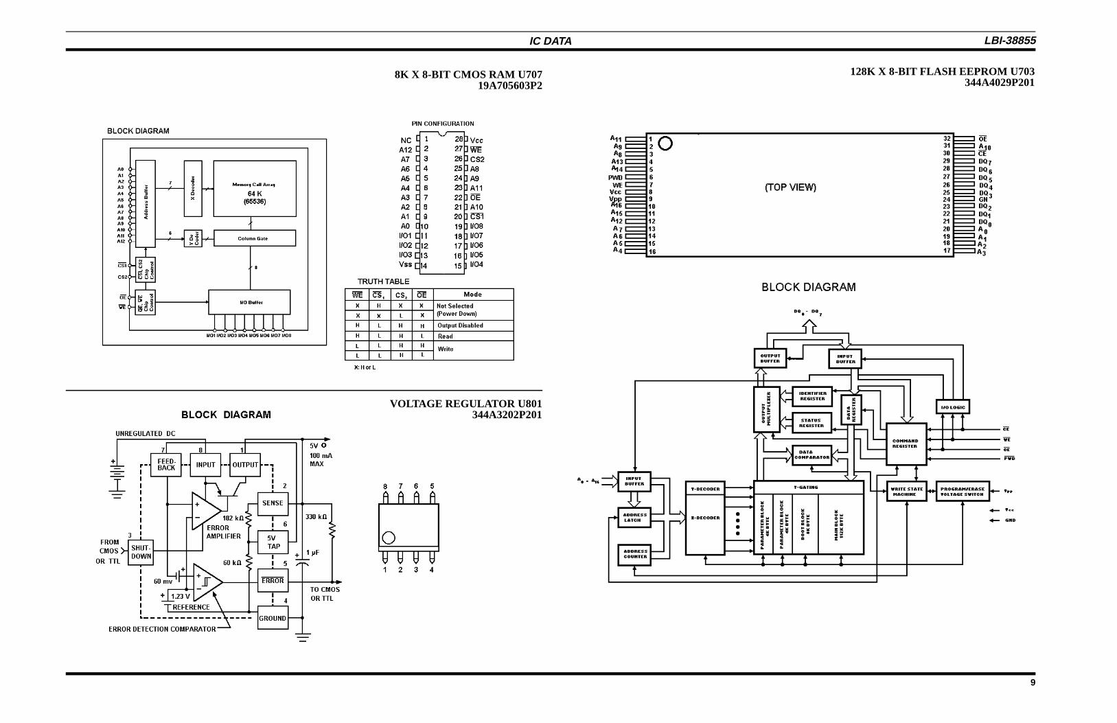
5 Volt Regulator U801 (sheet 1)
A single 5 volt regulator U801 supplies all circuitry on theboard (except OP Amp U301 and Audio PA U603). Theregulator receives input voltage from the battery (nominally7.5 Vdc) on J801-4. D801 on J801-4 provides reverse polarityprotection.
The regulator also provides a reset signal if the inputvoltage falls below 5.2 Vdc. At this point, the regulator willbegin to fall out of regulation and pin 5 will switch LOW (toground). This LOW will discharge capacitor C802 and turnON Q804. Q804 provides the active HIGH reset signal toModem U702.
When the input voltage to the regulator exceeds 5.2 Vdc(as when the radio is first turned ON), pin 5 switches to a highimpedance state. C802 provides a reset pulse delay by charg-ing through R806 and R807. When C802 charges to greaterthan 4.3 Vdc, Q804 turns OFF to release the reset signal tothe Modem.
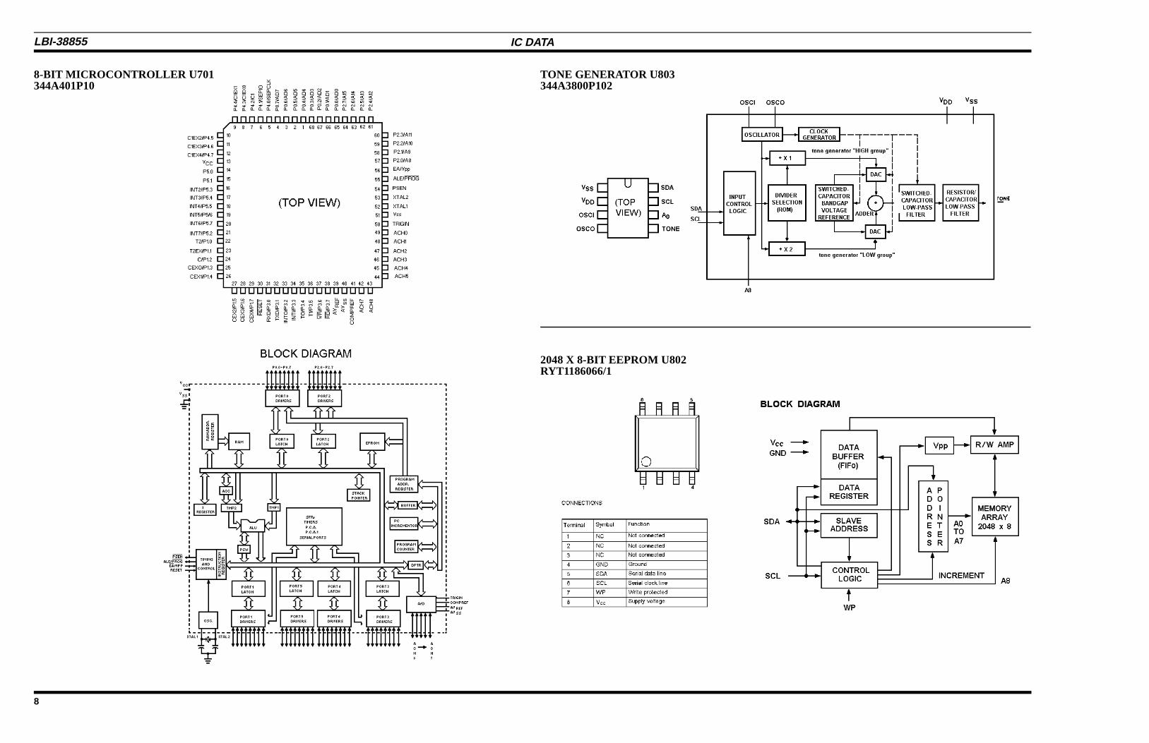
Personality EEPROM U802 (sheet 1)
A 2048 X 8 bit EEPROM U802 stores all customerfrequencies, tones and option information. Tracking dataaligned with the RF Board is stored for the transmit highpower level, transmit low power level, mic deviation, datadeviation and squelch.
The personality information in the EEPROM matches theunique number in Serial Number ROM U706. See the circuitdescription on the Serial Number ROM.
Copyright © December 1992, Ericsson GE Mobile Communications Inc.
If replacement of U802 personality EEPROM or U706Serial Number ROM is necessary, contact Ericsson Inc.Customer Service to obtain programming information.
NOTE
LBI-38855
1

The microprocessor serially communicates with theEEPROM on the IIC CLK and IIC DATA lines (or the InterIntegrated Circuit Bus). Programming of the EEPROM isaccomplished without opening the radio by communicatingwith the microprocessor through the UDC connector.
The MIC HI lead of the UDC connector is the RX DATAline which receives data from the programming computer.The PTT lead is the TX DATA line to the computer. With noexternal signal connected to MIC HI , a 2.5 Vdc bias voltagerests on this pin. Op amp U601.2 (on sheet 5) is setup as acomparator to sense the DC level on the MIC HI lead. Theoutput of the op amp is normally at a logic high level. Whendata pulls the MIC HI line low (below 1 Vdc), the op ampoutput switches low. The active low output (PROG RXDATA) feeds Microprocessor U701-31.
To PC program the EEPROM, the radio must be placedinto PC programming mode before communicating seriallyon the MIC HI and PTT lines. Software checks the status ofthe volume and channel switches at power up. If one of thevolume switches (UP or DOWN) along with one of thechannel switches (UP or DOWN) are pushed simultaneouslyat power up and then released, the radio enters PC program-ming mode. Power must be recycled OFF/ON to reset theradio to leave programming mode.
DTMF Encoder U803 (sheet 1)
DTMF (Dual Tone Multifrequency) tones are generatedby U803. Reference clock oscillator Y801 (3.579545 MHz)only runs while a tone is being generated with the transmitterkeyed. The encoder’s oscillator is disabled by software toprevent harmonic and other spurious energy from interferingwith the radio receiver. When a software command is sent intransmit to generate a tone, the clock oscillator recovers after3 ms and enables the DTMF generator.
The microprocessor serially communicates with theDTMF encoder on the IIC CLK and IIC DATA lines. Thegenerated tones from pin 5 are sent to the RX audio path (forspeaker sidetone) on ASP U804-29 (sheet 4). They are alsosent to the TX audio path on ASP U804-73 (sheet 5).
Low Battery Sense (sheet 1)
When the battery voltage drops below approximately 6.3Vdc, the BT pixel on the LCD turns on. R801 and R802 dividethe battery voltage to one half. This low battery sense voltageis sent to microprocessor U701 pin 44. This pin is an analoginput port to the microprocessor which is used to measure thevoltage level. D710 protects the microprocessor from overvoltage conditions on the battery line.
Microprocessor U701 (sheet 2)
A single microprocessor (U701) controls the operation ofthe PCS radio. All microprocessor lines which connect to theanalog portion of the board or connect externally to the boardare first RF bypassed by RC circuits. Most of these RCcircuits are shown on the other sheets of the schematic but arephysically located as close as possible to each microprocessorpin on the bottom of the PC board.
The microprocessor contains internal "masked" softwarecode to handle the programming of Flash Memory U703. Fornormal radio operation, this software code is not needed. Themicroprocessor normally executes the radio software code inthe Flash memory. The external address pin 56 is normallylow to address the Flash memory. The internal memory is onlyused during Flash programming. See the Flash Memory de-scription below.
To check the operation of the microprocessor, check thatthe buffered 11.0592 MHz clock from Modem U702 is pre-sent on pin 52. The ALE output line (pin 55) should then runcontinuously at 1.8432 MHz (0.54 µs period on a scope). ThePSEN output (pin 54) also runs continuously at the samefrequency; however, PSEN rests at 5 volts when 12 Vdc isapplied to the radio during Flash Memory programming.
Flash Memory U703 (sheet 2)
The radio operating system software for the microproces-sor resides in U703, a 128 kilobyte Flash Memory device. TheFlash Memory allows easy reprogramming of the radio soft-ware for additional features and software upgrades withoutopening the radio or removing standard EPROMs.
The Flash Memory may be reprogrammed through thesame PC computer interface that programs the personalityEEPROM. See the previous section on the personalityEEPROM for a description on the PC data interface.
When the Flash Memory is programmed, 12.0 ±4.5 Vdcis applied to the battery terminals. This voltage is sensed byQ801/Q802 and is applied to the Flash. Also this voltage isdivided down to 5V by R726/R727 to feed the externaladdress pin 56 of the microprocessor. With this pin high, theinternal "boot code" software masked inside the microproc-essor is executed. This "boot code" software handles runningthe microprocessor to serially communicate with the PCcomputer to program the Flash.
The radio checks for 12 volts, only at power-up. The supplyvoltage must be at 12 volts within 20 ms after power-up toprevent U701 from disabling Q801. U701-9 is low at power-upto enable the Q801 sensing circuit. Pin 9 remains low if pin 56is high. If Q801 does not sense 12V, pin 56 will be low, causingthe radio software to immediately switch pin 9 high to disableQ801. Disabling Q801 prevents any momentary high batteryvoltage conditions from executing instructions out of the inter-nal "boot code" software.
Modem U702 (sheet 2)
Modem U702 performs several functions. The modem’schief function is to perform the serial to parallel and parallel toserial data conversion for receiving and transmitting data re-spectively. Limited high speed data from ASP U804 (sheet 4)feeds U702-23. Data for transmission on U702-26 is sent to thetransmit audio portion of the ASP (sheet 5).
The modem contains a latch which is used with the micro-processor ALE (address latch enable) line to demultiplex theaddress/data bus from the microprocessor. Address information(A0-A7) is separated from the address/data bus and then sent tothe Flash Memory and the RAM.Another function of the mo-dem is to provide an address decoder for selecting the modemand the RAM. Q704.1 and Q704.2 form a NAND gate whichenables the decoder (active high) on U702-24 whenever the reador write lines are active low.
The modem also provides the reset signal (U702-43) for themicroprocessor and the ASP. The active high reset is invertedby Q703 to be sent to the active low reset inputs of the micro-processor (U701-30) and the ASP (U804-9). A 2 second "watchdog timer" inside the modem must be continually reset by theoperating software or a 50 ms reset pulse will be sent to themicroprocessor if a software failure occurs. Also, the modem
receives the reset signal from the 5 volt regulator (U702-33)which is passed to the microprocessor reset.
The 11.0592 MHz clock oscillator is also provided by themodem using Y701. The buffered clock signal (U702-15) is sentto the microprocessor and the ASP. Q702 can provide a clockfrequency shift if needed. Normally Q702 is turned off withC735 out of the oscillator circuit (except for the off capacitanceof Q702). If a harmonic of the logic circuitry falls on a receiverchannel, the clock can be shifted to move the interference.
Serial Number ROM U706 (sheet 2)
The Serial Number ROM (Read Only Memory) U706 con-tains a unique 48 bit number which is read by the microproces-sor at power up. A single pin on the device provides serialcommunication with the microprocessor as well as +5 Vdcpower through R728.
For proper radio operation, the unique serial number mustmatch the personality information in EEPROM U802. Replac-ing either device may disable operation on all programmedEDACS systems. Conventional and GEMARC systems willcontinue to function normally. The radio must be reprogrammedbased upon the serial number.
RAM U707 (sheet 2)
U707 is a high speed static RAM (Random Access Memory)providing 8 kilobytes of temporary data storage for the micro-processor. The RAM receives the lower 8 bits of address (A0-A7) from the demultiplexer latch inside the modem. Chip select(pin 20) is also provided by the address decoder in the modem.
Audio Signal Processor (sheets 3, 4, & 5)
The Audio Signal Processor (ASP) U804 handles nearly allaudio functions in the PCS radio. Three sheets of the schematicdiagram divide the ASP into three major blocks. A simplifiedblock diagram of the ASP internal circuitry is shown on eachschematic sheet for reference. Internal audio switches, filters,controls, etc. are labeled with the ASP software register states(High or Low) for reference only.
The Flash Memory requires a precise voltage of 11.5 to 12.5volts for proper programming. This voltage is applied tothe radio’s normal battery terminals. Damage to the FlashMemory as well as other devices will result if the batteryvoltage exceeds 12.5 volts.
WARNING
12V must be applied to the radio with a fast rise time (within20 ms). Some power supplies rise too slowly when turnedon. If the radio powers up in normal operating mode,manually connect 12V to the radio with the supply alreadyon.
NOTE
If replacement of U706 Serial Number ROM or U802personality EEPROM or is necessary, contact Ericsson Inc.Customer Service to obtain programming information.
NOTE
LBI-38855
2

EDACS & Conventional Modes RX Audio (sheet 4)
Detector audio enters ASP pin 44, the (-) input of an op ampbuffer. R609 and R610 set the gain of the op amp. Since pin 44is at "virtual ground" for the op amp, the signal level here willnot be measurable.
In the ASP, the buffered detector audio is bandpass filtered(300 to 3000 Hz). The filtered audio is selected by ISA/ISBaudio multiplex switch in the ASP and then passes through thedeemphasis stages. The deemphasized audio passes through thedigital volume control, through audio switch RXO, and thenleaves on ASP pin 27. The receive audio path for the EDACSand conventional modes never loops out and back into the ASP.
Receive audio leaves the ASP and feeds U603 audio PA.DCpower to the PA is controlled by ASP pin 18 (SW0).
High Speed Data Limiter (sheet 4)
Buffered, unfiltered detector audio in the ASP passesthrough audio gate TDS to ASP pin 45. Busy tone decode switchQ603 is normally OFF (SW5 = 1) to pass data through R612 tothe high speed limiter (+) input on ASP pin 32. The average DClevel of the data signal is sent to the limiter (-) input on ASP pin31 as a reference for the comparator. R611 and C605 filter thesignal component to provide the DC reference.
The output of the limiter ASP pin 21 is inverted by Q602.The data is sent to the modem for data decoding and also sentto microprocessor U701 port 4.2. This port is normally high.The port is switched low during transmit to clamp limited noiseto the modem.
Q601 allows the high speed and low speed limiters to settlequickly when a RF signal appears that differs from the receiverfrequency. A 5-10 ms pulse (active low) is sent to Q601 beforeattempting to read any data from the limiters to quickly chargeC601 to the operating DC level.
Low Speed Tone/Data Decoding (sheet 4)
In the ASP, buffered detector audio passes through switchTX to feed the 105/210 Hz low pass filter for removing voicesignals fromthe low frequency Channel Guard tones or data.The filter cut off is 105 Hz for tones equal to or less than 105Hz. For tones above 105 Hz or for data, the 210 Hz low passfilter is selected.
The output of the 105/210 Hz filter passes through audioswitch CGE, and out of the ASP on pin 37.The tones/data feedASP pin 35, the (+) input of the low speed comparator limiter.The average DC level of the tones/data signal is sent to ASP pin34 as a reference to the comparator (-) input. R618 and C610filter the signal to provide the DC reference. The output of the
limiter on ASP pin 22 is sent to microprocessor U701 Port 4.3for decoding.
GEMARC Mode RX Audio (sheet 4)
Detector audio enters ASP pin 44. In the ASP, detector audiois bandpass filtered (300-3000 Hz) and is passed out to ASP pin45 through switch TDS. The filtered receive audio from the ASPis sent to U602 which is a digital switch capacitance notch filter.The notch frequency is determined by ceramic resonators Y601or Y602 to notch either the standard (3052 Hz) or alternate(2918 Hz) busy tones. Microprocessor port 1.0 selects eitherresonator.
The notched receive audio is sent to ASP pin 28 and isselected with ISA/ISB multiplex audio switch. The deempha-sized audio passes through the digital volume control, throughaudio switch RXO, and then leaves on ASP pin 27 which feedsthe audio PA.
GEMARC Tone Decoding (sheet 4)
Detector audio is bandpass filtered (300-3000 Hz) in theASP and passed out through switch TDS on ASP pin 45. Thisaudio feeds the notch filter U602, bandpass filter (U301.2 andU601.1), and the high speed limiter.
For signalling tone decode, busy tone decode switch Q603is OFF (SW5 = 5 Vdc). Wide band audio is passed from the ASPthrough R612 to the high speed limiter (+) input on ASP pin 32.The average DC level of the audio signal is sent to the limiter(-) input on ASP pin 31 as a reference for the comparator. Theoutput of the limiter on ASP pin 21 is sent to microprocessorU701-7 port 4.2 for tone decoding.
For busy tone decode, bandpass filtered audio at the busytone frequencies feeds the high speed limiter through Q603. The3 kHz low pass filtered audio from ASP pin 45 provides someof the high frequency roll off of the bandpass response. U301.2provides a notch at 2.3 kHz plus a high pass response to rejectvoice frequencies. U601.1 is a bandpass filter centered at 3 kHz.
For busy tone decoding, busy tone decode switch Q603 isON (SW5 = 0). Bandpass filtered audio from U601.1 is passedto the limiter. The low impedance output of U601.1 effectivelyshorts the wide band audio through R612. Busy tone decodingis also done on microprocessor U701-7 port 4.2.
Receive Noise Squelch (sheet 3)
The squelch circuit monitors the level of high frequencynoise on the receiver detector audio to determine if a carrier isquieting the receiver. A Digital to Analog converter in the ASPsets the threshold level required to operate the squelch circuit(normally 8 dB SINAD). When the noise falls below the thresh-
old level, the carrier activity sensor (CAS) output switches to0 Vdc. The CAS signal feeds the microprocessor U701 analogport on pin 43.
Buffered, unfiltered detector audio leaves at ASP pin 43and feeds ASP pin 50 which is the high pass filter input (7.5kHz). In the ASP, the high pass filtered audio is rectified andsent out on ASP pin 52. The rectified noise is filtered toprovide an average DC level proportional to the noise level.This DC noise level is applied to a noninverting DC bufferamp on ASP pin 55. The output of the amp is on ASP pin 53.The gain of the DC amp is set by R620, R622, R623, andthermistor RT601. The thermistor increases in resistance atcold temperatures, causing the DC amp gain to increase. Thiscompensates for the RF Board detector output level droppingat colder temperatures.
The buffered DC noise level output is sent to the (-)comparator input on ASP pin 49. The comparator (+) inputreceives a reference voltage from the digital to analog con-verter. When the DC noise level falls below the comparatorreference, the comparator output switches high. The compa-rator output is buffered and inverted and appears at ASP pin23. This CAS output is normally high (+5 Vdc) and switcheslow (0 Vdc) when a signal is detected.
To tighten the squelch, the D/A reference voltage is low-ered. Hysteresis for the squelch is done in software. When thesquelch output switches to indicate a signal is detected, theD/A reference value is increased slightly to loosen thesquelch. The hysteresis eliminates "bubbling" or chatteringnoise in the speaker. The "bubbling" would normally becaused by transitional changes in the DC noise level aroundthe reference point.
Transistor Q604.1 is normally turned ON with ASP pin16 (SW2 = 1) at +5 Vdc, placing C611 in the DC noiseaveraging circuit. C611 provides a conventional slow (60 ms)squelch operation to prevent chopping the audio with rapidsquelch closings in weak signal areas. When Q604.1 isturned OFF, a 5 ms fast squelch is provided by only C610.
Receive Alert Tones (sheet 4)
Programmable alert tones are generated in the ASP. TheASP uses a 66.6 kHz clock divided by 2 and then divided bya 6 bit divider. Therefore, the lowest alert tone frequency thatcan be generated is 33.3k / 63 = 528 Hz.
The output of the alert tone divider is on ASP pin 76. Thetone output connects to ASP pin 30 to feed the ISA/ISB audiomultiplex switch in the receive audio path. The tones thenpass through unused audio switch VG which is hardwired(logic low) to pass the tones through the deemphasis stages.The deemphasized audio passes through the digital volume
control, through audio switch RXO, and then leaves on ASPpin 27 which feeds the audio PA.
Transmit Mic Audio (sheet 5)
The microphone receives 2.5 Vdc bias through R315. Micaudio is coupled into ASP pin 74. Mic audio passes throughaudio switch MIS to the mic amplifier. Switch MGS deter-mines the gain of the amplifier. MGS is normally open (MGS= 1) for high gain. A LOW MIC GAIN option in PC program-ming can lower the gain 10 dB for noisy environments whenMGS is closed. The audio from the mic amp is then preem-phasized and 300 Hz high pass filtered in the ASP. The audiothen leaves the ASP on pin 70.
Preemphasized mic audio is coupled back into the ASP onpin 57. The audio is passed through muting switch AEN andthen feeds the limiter. The limiter threshold can be stepped upby register LMT so that the peak deviation of the mic audiocan be increased when no Channel Guard is present.
Limited mic audio then passes through a summing amp inthe ASP which sums tones and data. The output of the sum-ming amp feeds switch PBY to allow a choice of passing theaudio through the 3 kHz post limiter filter (for limited micaudio) or passing unfiltered audio (for data) directly to thetransmit deviation control (TA5 - TA0). The output of thedigital deviation control passes through audio switch TXO toASP pin 60.
The TX audio output from the ASP feeds U301.1 whichprovides two functions. U301.1 provides some of the lowfrequency equalization for the synthesizer by increasing ingain 6 dB/octave below 15 Hz. This low frequency gain helpscompensate and flatten out the low frequency roll-off nor-mally experienced when modulating the VCO in RF synthe-sizers. Another function of U301.1 is a second order (12dB/octave) low pass filter to help attenuate any out of bandnoise above approximately 8 kHz from the ASP. The cutoffis high enough not to degrade 9600 baud data transmission.The output of U301.1 is DC coupled to the RF Board to feedthe synthesizer.
Transmit RF Output Power (sheet 3)
The D/A converter used to set the squelch threshold inreceive and is used to set the power level in transmit. The D/Aoutput is on ASP pin 48. The output voltage level can varyfrom 0 to 5 Vdc in 256 steps to control the transmit power.
Transmit High Speed Data (sheet 5)
Modem data is applied to ASP pin 80. CEN registers selectthe TX DATA input. The data is passed through a bessel filterin the ASP. The output of the filter is sent to the TX path
LBI-38855
3
summing amp. The output of the summing amp feeds audioswitch PBY to allow bypassing the 3 kHz post limiter filterfor data transmission. The data passes through the digitaldeviation control and then through audio switch TXO to feedU301.1 and the synthesizer. U301.1 provides low frequencygain equalization for data transmission. See the Transmit MicAudio section for a U301.1 circuit description.
During transmit, the modem input from the receive datalimiter requires muting to prevent the modem from beingdisturbed by receive noise. Microprocessor U701 Port 4.2switches low during transmit to clamp the line to ground.
Transmit CG Tones and Low Speed Data (sheets 4 & 5)
Microprocessor U701 generates the low frequency Chan-nel Guard tones/data on WB1 and WB2. These two bits arealso used to generate GEMARC signalling tones (see sectionon TRANSMIT GEMARC SIGNALLING TONES). Thetwo bit low frequency tones/data are summed into ASP pin38. The stepped tones or data pass through audio switch TXto a 105/210 Hz low pass filter. The filter has a cutoff of 105Hz for tones equal to or less than 105 Hz. For data or tonesabove 105 Hz, the 210 Hz filter is selected.
The filtered tones/data pass through gate CGE, then outof the ASP on pin 37, through R317, and back into the ASPon pin 58 (CGIN). GEMARC busy tone is also fed into thispin through C310. The impedance of C310 is high enough atlow frequencies to prevent any loading of the tones/datathrough R317. See the section on Transmit GEMARC BusyTone.
In the ASP, the filtered tones/data pass from pin 58(CGIN) through audio switch BEN to feed the transmit sum-ming amp. The output of the summing amp feeds switch PBYto allow switching the 3 kHz post limiter filter in line. Theoutput of the post limiter passes through the digital deviationcontrol, through switch TXO, and then out of the ASP toU301.1. U301.1 provides low frequency gain equalization fordigital Channel Guard transmission. See the Transmit MicAudio section for a U301.1 circuit description.
Transmit GEMARC Signalling Tone (sheets 4 & 5)
Microprocessor U701 generates the GEMARC signallingtones on WB1 and WB2. These two bits are also used togenerate low frequency Channel Guard tones/data (see sec-tion on TRANSMIT CG TONES AND LOW SPEED DATA).The 2 bit generated GEMARC tones feed ASP pin 59. Feed-ing the GEMARC tones here allow using ASP audio switchDEN to mute the unfiltered WB1 and WB2 signal whenChannel Guard is generated in EDACS and conventionalmodes.
In the ASP, the tones pass through audio switch DEN andare sent to the summing amp in the TX audio path. The tonesare routed to the 3kHz post limiter filter through audio switchPBY. The tones are filtered, sent through the digital deviationcontrol, audio switch TXO, and then out of the ASP on pin60.
Transmit DTMF (sheet 4,5)
U803 generates DTMF tones which feed the ASP on pin73. In the ASP, audio gate MIS passes the DTMF tones to themic amp while muting the mic audio. Switch MGS deter-mines the mic amp gain and must be set to 1 to open the switchfor high gain. The amplified DTMF tones are then preem-phasized and follow the same path as the mic audio in the ASP(see section on MIC AUDIO).
For receive audio sidetone, the DTMF audio is also fedinto ASP pin 29. The sidetone audio is selected by theISA/ISB receive audio multiplex switch and then passesthrough unused audio switch VG which is hard-wired (logiclow) to pass the audio through the deemphasis stages. Thedeemphasized audio passes through the digital volume con-trol, through audio switch RXO, and then leaves on ASP pin27 which feeds the audio PA.
Transmit GEMARC Busy Tone (sheet 5)
Microprocessor U701 generates either the 3052 Hz(standard) or the 2918 Hz (alternate) busy tone on port 1.5.The square wave busy tone is summed into the TX audio pathat the same point as the low frequency CG tones/data at ASPpin 58 (CGIN). R753 and R316 determine the 1 kHz devia-tion level of the tone. C310 couples the high frequency toneinto the ASP. The tone follows the same path in the ASP asthe CG tones/data, through switch BEN and into the TX audiosumming amp.
DUAL FORMAT PCS FRONT ASSEMBLY19D902177G13 SYSTEM
19D902177G15 SCANISSUE 4
*COMPONENTS, ADDED, DELETED OR CHANGED BY PRODUCTION CHANGES
SYMBOL PART NUMBER DESCRIPTION
A2 AUDIO/LOGIC BOARD19D903568G1
- - - - - - - - CAPACITORS- - - - - - - -
C303 19A702052P134 Ceramic: 0.1 µF ±5%, 25 VDCW.thruC305
C306 19A705205P2 Tantalum:1 µF, 16 VDCW; sim toSprague 293D.
C307 19A702052P134 Ceramic: 0.1 µF ±5%, 25 VDCW.
C308 19A702052P130 Ceramic: .022 µF ±5%, 50 VDCW.
C309 19A702052P45 Ceramic: 0.22 µF ±10%, 16 VDCW.
C310 19A149896P121 Ceramic: 0.1 µF ±10%, 50 VDCW.
C311 19A149896P7 Ceramic: 680 pF ±10%, 50 VDCW.
C312 19A705205P19 Tantalum: 2.2 µF, 10 VDCW; sim toSprague 293D.
C313 19A149897P45 Ceramic:180 pF ±5%, 50 VDCW.
C601 19A705205P2 Tantalum:1 µF, 16 VDCW; sim toSprague 293D.
C602 19A149896P121 Ceramic:.01 µF ±10%, 50 VDCW.
C603 19A149896P15 Ceramic:3300 pF ±5%, 50 VDCW.andC604
C605 19A705205P2 Tantalum:1 µF, 16 VDCW; sim toSprague 293D.
C606 19A149896P17 Ceramic:4700 pF ±5%, 50 VDCW.
C607 19A149896P121 Ceramic:.01 µF ±10%, 50 VDCW.
C608 19A702052P134 Ceramic: 0.1 µF ±5%, 25 VDCW.andC609
C610 19A705205P6 Tantalum:10 µF, 16 VDCW; sim toSprague 293D.
C611 19A705205P2 Tantalum:1 µF, 16 VDCW; sim toSprague 293D.
C612 19A702052P134 Ceramic: 0.1 µF ±5%, 25 VDCW.
C613 19A705205P19 Tantalum:2.2 µF, 10 VDCW; sim toSprague 293D.
C614 19A705205P2 Tantalum:1 µF, 16 VDCW; sim toSprague 293D.
C615 19A702052P134 Ceramic: 0.1 µF ±5%, 25 VDCW.
C616 19A149897P39 Ceramic:100 pF ±5%, 50 VDCW,temp coef 0 ±30 PPM.
C617 19A149896P121 Ceramic:.01 µF ±10%, 50 VDCW.
C618 19A705205P2 Tantalum:1 µF, 16 VDCW; sim toSprague 293D.
C619 19A149896P121 Ceramic:.01 µF ±10%, 50 VDCW.
C620 19A705205P6 Tantalum:10 µF, 16 VDCW; sim toSprague 293D.
C621 19A702052P134 Ceramic: 0.1 µF ±5%, 25 VDCW.andC622
C623 19A149897P43 Ceramic:150 pF ±5%, 50 VDCW,temp coef 0 ±30 PPM.
SYMBOL PART NUMBER DESCRIPTION
C624 19A149896P51 Ceramic:330 pF ±5%, 50 VDCW.
C625 19A149896P9 Ceramic:1000 pF ±5%, 50 VDCW.andC626
C627 19A149896P15 Ceramic:3300 pF ±5%, 50 VDCW.
C628 19A149896P17 Ceramic:4700 pF ±5%, 50 VDCW.
C701 19A149897P47 Ceramic:220 pF ±5%, 50 VDCW,and temp coef 0 ±30 PPM.C702
C703 19A149897P39 Ceramic:100 pF ±5%, 50 VDCW,and temp coef 0±30 PPM.C704
C705 19A149897P47 Ceramic:220 pF ±5%, 50 VDCW,thru temp coef 0 ±30 PPM.C708
C709 19A149897P39 Ceramic:100 pF ±5%, 50 VDCW,and temp coef 0 ±30 PPM.C710
C711 19A149897P47 Ceramic:220 pF ±5%, 50 VDCW,thru temp coef 0 ±30 PPM.C715
C717 19A149897P47 Ceramic:220 pF ±5%, 50 VDCW,thru temp coef 0 ±30 PPM.C721
C725 19A149897P47 Ceramic:220 pF ±5%, 50 VDCW,and temp coef 0 ±30 PPM.C726
C727 19A705205P6 Tantalum:10 µF, 16 VDCW; sim toSprague 293D.
C728 19A702052P134 Ceramic: 0.1 µF ±5%, 25 VDCW.andC729
C730 19A149897P47 Ceramic:220 pF ±5%, 50 VDCW,temp coef 0 ±30 PPM.
C731 19A705205P6 Tantalum:10 µF, 16 VDCW; sim toSprague 293D.
C732 19A149897P47 Ceramic:220 pF ±5%, 50 VDCW,and temp coef 0 ±30 PPM.C733
C734 19A702052P134 Ceramic: 0.1 µF ±5%, 25 VDCW.
C735 19A149897P21 Ceramic:18 pF ±5%, 50 VDCW, temp coef 0 ±30 PPM.
C736 19A149897P47 Ceramic:220 pF ±5%, 50 VDCW,and temp coef 0 ±30 PPM.C737
C738 19A149897P15 Ceramic:10 pF ±5%, 50 VDCW, temp coef 0 ±30 PPM.
C739 19A149897P27 Ceramic:33 pF ±5%, 50 VDCW, temp coef 0 ±30 PPM.
C740 19A149897P47 Ceramic:220 pF ±5%, 50 VDCW,thru temp coef 0 ±30 PPM.C750
C751 19A149897P39 Ceramic:100 pF ±5%, 50 VDCW,temp coef 0 ±30 PPM.
C752 19A149897P47 Ceramic:220 pF ±5%, 50 VDCW,temp coef 0 ±30 PPM.
C753 19A149897P15 Ceramic:10 pF ±5%, 50 VDCW,temp coef 0 ±30 PPM.
C754 19A149897P27 Ceramic:33 pF ±5%, 50 VDCW, and temp coef 0 ±30 PPM.C755
PARTS LISTLBI-38855
4

SYMBOL PART NUMBER DESCRIPTION
C801 19A705205P2 Tantalum:1 µF, 16 VDCW; sim toSprague 293D.
C802 19A702052P134 Ceramic: 0.1 µF ±5%, 25 VDCW.
C803 19A702052P45 Ceramic: 0.22 µF ±10%, 16 VDCW.
C805 19A702052P134 Ceramic: 0.1 µF ±5%, 25 VDCW.
C806 19A149897P47 Ceramic: 220 pF ±5%, 50 VDCW,temp coef 0 ±30 PPM.
C808 19A705205P6 Tantalum:10 µF, 16 VDCW; sim toSprague 293D.
-- - - - - - - DIODES - - - - - - - -
D701 19A700053P2 Silicon: 2 Diodes in Series; sim to thru BAV99.D710
D720 19A705377P5 Silicon, Hot Carrier: sim to HSMS-2804.
D801 344A3326P1 Surface mount, rectifier.
- - - - - - - - JACKS- - - - - - - -
J801 19A705482P1 Printed wire, 2-part; sim to SAMTEC SSW-112-01-SS.
J802 Part of printed wire board 19D903569P1.
J901 Part of printed wire board 19D903569P1.
- - - - - - - - TRANSISTORS- - - - - -
Q601 19A700059P2 Silicon, PNP: sim to MMBT3906, low profile.
Q602 19A700076P2 Silicon, NPN: sim to MMBT3904, low profile.
Q603 19A700059P2 Silicon, PNP: sim to MMBT3906,low profile.
Q604 19A705945P2 Silicon, Dual NPN: sim to R OHM IMX3.
Q605 19A134577P2 Silicon, PNP: sim to Phillips BCX51-16.
Q606 19A703197P2 Silicon, PNP; sim to MMBT4403 low profile.
Q607 19A702503P3 Silicon, NPN: sim to BFS17, low profile.
Q701 19A705945P2 Silicon, Dual NPN: sim to R OHM IMX3.
Q702 19A700076P2 Silicon, NPN: sim to MMBT3904, and low profile.Q703
Q704 19A705945P2 Silicon, Dual NPN: sim to R OHM IMX3.
Q801 19A700076P2 Silicon, NPN: sim to MMBT3904, low profile.
Q802 19A700059P2 Silicon, PNP: sim to MMBT3906, low profile.
Q804 19A700059P2 Silicon, PNP: sim to MMBT3906,low profile.
- - - - - - - RESISTORS- - - - - - -
R301 19A149818P153 Metal film: 15K ohms ±5%, 1/16 w.
R303 19A149818P102 Metal film: 1K ohms ±5%, 1/16 w.
R304 19A149818P104 Metal film: 100K ohms ±5%, 1/16 w.
R305 19A149818P102 Metal film: 1K ohms ±5%, 1/16 w.
R306 19A149818P104 Metal film: 100K ohms ±5%, 1/16 w.
R307 19A149818P154 Metal film: 150K ohms ±5%, 1/16 w.
SYMBOL PART NUMBER DESCRIPTION
R308 19A149818P333 Metal film: 33K ohms ±5%, 1/16 w.
R309 19A149818P224 Metal film: 150K ohms ±5%, 1/16 w.
R310 19A149818P683 Metal film: 68K ohms ±5%, .063 watts at 70°C.
R313 19A149818P153 Metal film: 15K ohms ±5%, 1/16 w.
R314 19A149818P470 Metal film: 47 ohms ±5%, 1/16 w.
R315 19A149818P561 Metal film: 560 ohms ±5%, 1/16 w.
R316 19A149818P103 Metal film: 10K ohms ±5%, 1/16 w.
R317 19A149818P682 Metal film: 6.8K ohms ±5%, 1/16 w.
R601 19A149818P103 Metal film: 10K ohms ±5%, 1/16 w.andR602
R603 19A149818P104 Metal film: 100K ohms ±5%, 1/16 w.
R604 344A3304P1001 Metal film: 1K ohms ±1%, 1/10 w.
R605 19A149818P823 Metal film: 82K ohms ±5%, 1/16 w.
R606 19A149818P223 Metal film: 2K ohms ±5%, 1/16 w.
R607 344A3304P2493 Metal film: 249K ohms ±1%, 1/10 w.
R608 19A149818P333 Metal film: 33K ohms ±5%, 1/16 w.
R609 19A149818P104 Metal film: 100K ohms ±5%, 1/16 w.
R610 19A149818P683 Metal film: 68K ohms ±5%, .063 watts at 70°C.
R611 19A149818P103 Metal film: 10K ohms ±5%, 1/16 w.andR612
R613 19A149818P473 Metal film: 47K ohms ±5%, 1/16 w.andR614
R615 19A149818P103 Metal film: 10K ohms ±5%, 1/16 w.andR616
R617 19A149818P153 Metal film: 15K ohms ±5%, 1/16 w.
R618 19A149818P103 Metal film: 10K ohms ±5%, 1/16 w.andR619
R620 19A149818P184 Metal film: 180K ohms ±5%, 1/16 w.
R622 19A149818P334 Metal film: 330K ohms ±5%, 1/16 w.
R623 19A149818P154 Metal film: 150K ohms ±5%, 1/16 w.
R624 19A149818P683 Metal film: 68K ohms ±5%, 1/16 w.
R625 19A149818P104 Metal film: 100K ohms ±5%, 1/16 w.
R626 19A149818P473 Metal film: 47K ohms ±5%, 1/16 w.
R627 19A149818P222 Metal film: 2.2K ohms ±5%, 1/16 w.
R628 19A149818P223 Metal film: 22K ohms ±5%, 1/16 w.
R629 19A149818P153 Metal film: 15K ohms ±5%, 1/16 w.
R630 19A149818P4R7 Metal film: 4.7 ohms ±5%, .063 watts and at 70°C.R631
R632 19A149818P105 Metal film: 1M ohms ±5%, 1/16 w.
R634 19A149818P104 Metal film: 100K ohms ±5%, 1/16 w.
R635 19A149818P473 Metal film: 47K ohms ±5%, 1/16 w.
R636 19A149818P153 Metal film: 15K ohms ±5%, 1/16 w.
R637 19A149818P223 Metal film: 22K ohms ±5%, 1/16 w.
R638 19A149818P472 Metal film: 4.7K ohms ±5%, 1/16 w.
R639 19A149818P103 Metal film: 10K ohms ±5%, 1/16 w.
R640 344A3304P3483 Metal film: 348K ohms ±1%, 1/10 w.
R641 344A3304P1002 Metal film: 10K ohms ±1%, 1/10 w.
SYMBOL PART NUMBER DESCRIPTION
R642 19A149818P684 Metal film: 680K ohms ±5%, 1/16 w.
R701 19A149818P561 Metal film: 560 ohms ±5%, 1/16 w.thruR720
R725 19A149818P100 Metal film: 10 ohms ±5%, 1/16 w.
R726 19A149818P153 Metal film: 15K ohms ±5%, 1/16 w.
R727 19A149818P103 Metal film: 10K ohms ±5%, 1/16 w.
R728 19A149818P682 Metal film: 6.8K ohms ±5%, 1/16 w.
R730 19A149818P104 Metal film: 100K ohms ±5%, 1/16 w.thruR732
R733 19A149818P333 Metal film: 33K ohms ±5%, 1/16 w.andR734
R735 19A149818P332 Metal film: 3.3K ohms ±5%, 1/16 w.
R736 19A149818P100 Metal film: 10 ohms ±5%, 1/16 w.thruR739
R740 19A149818P561 Metal film: 560 ohms ±5%, 1/16 w.
R741 19A149818P333 Metal film: 33K ohms ±5%, 1/16 w.
R742 19A149818P823 Metal film: 82K ohms ±5%, 1/16 w.
R743 19A149818P101 Metal film: 100 ohms ±5%, 1/16 w.
R744 19A149818P561 Metal film: 560 ohms ±5%, 1/16 w.thruR751
R752 19A149818P101 Metal film: 100 ohms ±5%, 1/16 w.
R753 19A149818P272 Metal film: 2.7K ohms ±5%, 1/16 w.
R770 19A149818P561 Metal film: 560 ohms ±5%, 1/16 w.
R771 19A149818P473 Metal film: 47K ohms ±5%, 1/16 w.andR772
R773 19A149818P104 Metal film: 100K ohms ±5%, 1/16 w.
R774 19A149818P473 Metal film: 47K ohms ±5%, 1/16 w.
R775 19A149818P472 Metal film: 4.7K ohms ±5%, 1/16 w.
R776 19A149818P473 Metal film: 47K ohms ±5%, 1/16 w.
R777 19A149818P683 Metal film: 68K ohms ±5%, .063 watts at 70°C.
R778 19A149818P272 Metal film: 2.7K ohms ±5%, 1/16 w.
R779 19A4149818P392 Metal film: 3.9K ohms ±5%, 1/16 w.
R801 19A149818P473 Metal film: 47K ohms ±5%, 1/16 w.andR802
R803 19A149818P104 Metal film: 100K ohms ±5%, 1/16 w.thruR807
R808 19A149818P473 Metal film: 47K ohms ±5%, 1/16 w.
R811 19A149818P104 Metal film: 47K ohms ±5%, 1/16 w.thruR815
R816 19A149818P473 Metal film: 47K ohms ±5%, 1/16 w.
R817 19A149818P104 Metal film: 100K ohms ±5%, 1/16 w.
R825 19A149818P184 Metal film: 180K ohms ±1%, 1/10 w.
R826 19A149818P104 Metal film: 100K ohms ±5%, 1/16 w.
R827 19A149818P473 Metal film: 47K ohms ±5%, 1/16 w.
R828 19A149818P103 Metal film: 10K ohms ±5%, 1/10 w.
R830 19A149818P100 Metal film: 10 ohms ±5%, 1/16 w.
R833 19A149818P104 Metal film: 100K ohms ±5%, 1/16 w.
SYMBOL PART NUMBER DESCRIPTION
R834 19A149818P105 Metal film: 1M ohms ±5%, 1/16 w.
R835 19A149818P823 Metal film: 82K ohms ±5%, 1/16 w.
R836 19A149818P223 Metal film: 22K ohms ±5%, 1/16 w.
- - - - - THERMISTOR- - - - -
RT601 19A705813P2 Thermistor: sim to AL03006-58.2K-97-G100.
- - - INTEGRATED CIRCUITS- - -
U301 19A702293P3 Linear: Dual Op Amp; sim to LM358D.
U601 19A702293P3 Linear: Dual Op Amp; sim to LM358D.
U602 344A3999P201 Linear: Notch Filter; sim to LMF90CC.
U603 19A705452P2 Linear: Audio Amplifier; sim to NJM 2073D.
U701 344A4014P10 Digital: 8-Bit Microcontroller; sim to N83C51GB.
U702 19A704727P6 Digital: Modem.
U703 344A4029P201 Digital: 128K x 8-Bit Flash EEPROM;sim to E28F001BX-T120.
*U706 RYT1186063/1 Digital: 48-Bit Serial Number ROM.
U707 19A705603P2 Digital: 8K x 8-Bit Static CMOS RAM; sim to uPD4464G-20U.
U801 344A3202P201 Linear: Voltage Regulator; sim to LP2951ACM.
U802 RYT1186066/1 EEPROM, 2048 X 8 Bit, CMOS.
U803 344A3800P102 Linear: Tone Generator; sim to PCD3312C.
U804 344A3291P1 Digital: Audio Signal Processor; sim to MB87780PFV-G-BND.
- - - - - - CRYSTALS - - - - - -
Y601 344A4261G2 Resonator: 613.5 kHz.
Y602 344A4261G1 Resonator: 586.5 kHz.
Y701 19A702511G64 Crystal unit, quartz: 11.0592 MHz.
Y801 19A702511G65 Crystal unit, quartz: 3.579545 MHz.
- - - - MISCELLANEOUS - - - -
NOTE: Refer to the Assembly Diagram on page 10 for the location of the following miscellaneous parts.
5 19A702364P310 Machine screw, TORX Drive: No. M3-0.5 x 10.
6 19B801570P2 Connector holder.
7 19A705662P1 Connector, Elastomeric.
8 19A702364P304 Machine screw, TORX drive, Pan Head.
FRONT CAP ASSEMBLY19D902180G6 (Used in G13, System)19D902180G8 (Used in G15, Scan)
A5 LCD ASSEMBLY19A705090G11
- - - - - - - - LEDS - - - - - - - -
H1 19C851660P3 Crystal display.
PARTS LIST LBI-38855
5
SYMBOL PART NUMBER DESCRIPTION
- - - - MISCELLANEOUS - - - -
NOTE: Refer to page 11 for the location of the following miscellaneous parts.
19A703685P3 LCD connector.
19B801569P1 Diffuser.
19C851719P2 Lens.
LCD DRIVER BOARD19C852194G1
- - - - - - DIODES - - - - - -
CR1 19A705713P1 LED, subminiature.thruCR4
- - - - - - - JACKS - - - - - - -
J2 Part of printed wire board.
- - - - - - - - PLUGS - - - - - - - -
P1 19B801235P13 Terminal strip.
P2 19B801235P3 Terminal strip.
- - - - - TRANSISTORS - - - - -
Q1 19A700059P2 Silicon, PNP: sim to MMBT3906, low profile.
Q2 19A700076P2 Silicon, NPN: sim to MMBT3904, low profile.
- - - - - RESISTORS - - - - -
R1 19A149818P104 Metal film: 100K ohms ±5%, 1/16 w.andR2
R3 19A149818P472 Metal film: 4.7K ohms ±5%, 1/16 w.
R4 19A149818P221 Metal film: 220 ohms ±5%, 1/16 w.andR5
R6 19A149818P104 Metal film: 100K ohms ±5%, 1/16 w.
R7 19A149818P473 Metal film: 47K ohms ±5%, 1/16 w.
INTEGRATED CIRCUITS
U1 344A3211P201 LCD Driver.
A6 CONTROL ASSEMBLY19A705090G10
- - - - - - CAPACITORS - - - - - -
C3 19A702052P3 Ceramic: 470 pF ±10%, 50 VDCW.thruC7
- - - - - - - JACKS - - - - - - -
J1 19A115834P1 Contact, electrical: sim to AMP 2-330808-8.
- - - - - - - METERS - - - - - - -
M1 19A701301P3 Cartridge: Electret.
SYMBOL PART NUMBER DESCRIPTION
- - - - - - SWITCHES - - - - - -
S1 19A705712P1 Subminiature.
S2 19A705712P2 Subminiature.
- - - - - MISCELLANEOUS - - - - -
NOTE: Refer to page 11 for the location of the following miscellaneous parts.
19A149926P2 Insulator.
19A705733P4 Control frame, circuitized.
19B801571P2 Dome switch.
19C851722P1 Boot, auxiliary jack.
- - - - - - MODULE - - - - - -
B902 19A149673P1 Round:Water Proof, 24 ohms, 1/2 w.; sim to Line Electric Co. VS-50W24.
- - - - MISCELLANEOUS - - - -
NOTE: Refer to page 11 for the location of the following miscellaneous parts.
5 19A702364P304 Machine screw, TORX drive, Pan Head.
8 19C851997P2 Gasket, Speaker.
10 19C851636P2 Switch pad.
26 19A705777P1 Nameplate.
28 19B801568P3 Insulator.
29 344A3854 P1 Insulator.
30 19B234763P22 Pad.
31 19C337135P1 Seal.
FRONT COVER ASSEMBLY19D902072G12 (SYSTEM Model)
NOTE: Refer to page 12 for the location of the following miscellaneous parts.
18 19A116318P4 Foil, Magnetic Shielding:1.50 inches wide.
19 19A705664P1 Gasket.
27 3 44A4654P1 Gasket.
34 19D902072P34 Fr ont cover.
37 19D902072P37 Front cover.
43 19D902072P43 Front cover.
33 KEYPAD BOARD19C852173G1
- - - - - CAPACITORS - - - - -
C780 19A702052P134 Ceramic: 0.1 µF ±5%, 25 VDCW.
C781 19A149897P39 Ceramic: 100 pF ±5%, 50 VDCW,thru temp coef 0 ±30 PPM.C783
- - - - - - DIODES - - - - - -
D780 19A700053P2 Silicon: 2 Diodes in Series; sim to thru BAV99.D791
SYMBOL PART NUMBER DESCRIPTION
- - - - - - JACKS - - - - - -
J780 Part of printed wire board.
- - - - - RESISTORS - - - - -
R780 19A149818P104 Metal film: 100K ohms ±5%, 1/16 w.thruR791
- - - INTEGRATED CIRCUITS - - -
U780 19A703987P322 Digital Logic, 8 Bit Shift Register; and sim to 74HC165.U781
21 FRONT COVER ASSEMBLY19D902072G14 (SCAN Model)
NOTE: Refer to page 12 for the location of the following miscellaneous parts.
17 19C851947P1 Printed wire board.
18 19A116318P4 Foil, Magnetic Shielding:1 .50 inches wide.
19 19A705664P1 Gasket.
27 344A4654P1 Gasket.
34 19D902072P34 Fr ont cover.
39 19D902072P39 Front cover.
41 19D902072P41 Front cover.
46 344A3087P11 Front cover.
47 19B801566P8 Shield.
PARTS LIST
PRODUCTION CHANGES
Changes in the equipment to improve performance or to simplify circuits areidentified by a "Revision Letter" which is stamped after the model number of theunit. The revision stamped on the unit includes all previous revisions. Refer to theParts List for the descriptions of parts affected by these revisions.
REV. A - AUDIO/LOGIC BOARD 19D903586G1
To improve 4800 Hz dotting frequency circuit and the alternate andstandard busy tone notch circuits. Changed C753, Q606, Q707, R636,R637 and R638.C753 was 19A149897P21 - Ceramic: 18 pF ± 5%, 50 VDCW.Q606 was 19A700052P2 - Silicon, PNP: sim to MMBT3906.Q607 was 19A700076P2 - Silicon, NPN: sim to MMBT3904.R636 was 19A149818P103 - Metal film: 10K ohms ± 5%, 1/16 w.R637 was 19A149818P103 - Metal film: 10K ohms ± 5%, 1/16 w.R638 was 19A149818P102 - Metal film: 1K ohms ± 5%, 1/16 w.
REV. B - AUDIO/LOGIC BOARD 19D903586G1
To improve high speed (9600 baud) reception, changed C605C605 was 19A705205P6 - Tantalum: 10 uF, 16 VDCW.
REV. C - AUDIO/LOGIC BOARD 19D903586G1
To improve the operation of the Microprocessor and the voltage sensingcircuit (Q801/Q802) when the radio is placed in a rapid charger with thepower switch ON. The PWB run from the emitter of Q801 to ground wasmoved to spare microprocessor pin 9.
REV. D - AUDIO/LOGIC BOARD 19D903586G1
Moved C605, C625, C626, C310, R816, R316, R625, R626, R828, R825and R641 to prevent interference to the speaker magnet. To improveoperation, the following components were changed, added or deleted.
Changed:
R825 was 19A149818P184 - Metal film: 180K ohms ± 1%, 1/10 w.R828 was 19A149818P103 - Metal film: 10K ohms ± 5%, 1/10 w.U802 was 19A805553P2 - EEPROM, 2048 x 8 Bit, CMOS sim to XICORX24C16.U805 was 19A705553P2 - Digital,CMOS: EEPROM sim to XICORX24C16.R624 was 19A149818P683 - Metal film: 68K ohms += 1%, 1/16 w.R301 was 19A149818P153 - Metal film: 15K ohms += 5%, 1/16 w.R317 was 19A149818P682 - Metal film: 6.8K ohms += 5%, 1/16 w.R753 was 19A149818P272 - Metal film: 2.7K ohms += 5%, 1/16 w.C310 was 19A149818P121 - Ceramic: 0.1 uF += 10%, 50 VDCW.R307 was 19A149818P224 - Metal film: 150K ohms += 5%, 1/16 w.C308 was 19A149818P130 - Ceramic: 0.22 uF += 5%, 50 VDCW.
Added:
Added R779, C756, R633, C629, R313, C314.
Deleted:
R720 was 19A149818P561 - Metal film: 560 ohms ± 5%, 1/16 w. C721was 19A149818P47 - Ceramic: 220 pF ± 5%, 50 VDCW.
REV. E - AUDIO/LOGIC BOARD 19D903568G1
To fix a cold temperature reset problem and notch filter failures, thefollowing components were changed:
C623 changed from 220 pF (19A149897P47) to 150 pF (19A149897P43).C624 changed from 470 pF (19A149896P5) to 330 pF (19A149897P51).Q607 changed from 19A700236P4 to 19A702503P3.R636 changed from 6.8K ohms (19A149818P682) to 15K ohms(19A149818P153)R637 changed from 6.8K ohms (19A149818P682) to 22K ohms(19A149818P223)R743 changed from 560K ohms (19A149818P561) to 100K ohms(19A149818P101)R779 changed from 2.7K ohms (19A149818P272) to 3.9K ohms(19A149818P392)
REV. F - AUDIO/LOGIC BOARD 19D903568G1
Old part no longer available. U706 was 344A4050P101. Changed toSerial ROM RYT1186063/1.
LBI-38855
6

OPERATIONAL AMPLIFIER U301, U60119A702293P3
NOTCH FILTER U602344A3999P201
AUDIO AMPLIFIER U60319A705452P2
MODEM U70219A704727P6
48-BIT SERIAL NUMBER ROM U706RYT1186063/1
IC DATA LBI-38855
7
8-BIT MICROCONTROLLER U701344A401P10
TONE GENERATOR U803344A3800P102
2048 X 8-BIT EEPROM U802RYT1186066/1
IC DATALBI-38855
8
8K X 8-BIT CMOS RAM U70719A705603P2
VOLTAGE REGULATOR U801344A3202P201
128K X 8-BIT FLASH EEPROM U703344A4029P201
IC DATA LBI-38855
9

AUDIO SIGNAL PROCESSOR U804344A3291P1
FRONT ASSEMBLY19D902177G13 & G15(19D902177, Sh. 2, Rev. 6)
ICDATA ASSEMBLY DIAGRAMLBI-38855
10
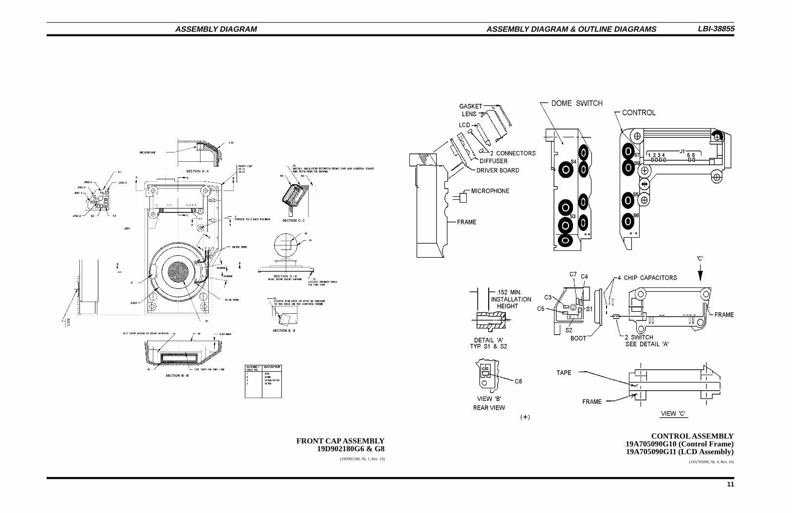
FRONT CAP ASSEMBLY19D902180G6 & G8
(19D902180, Sh. 1, Rev. 19)
CONTROL ASSEMBLY19A705090G10 (Control Frame)19A705090G11 (LCD Assembly)
(19A705090, Sh. 9, Rev. 16)
ASSEMBLY DIAGRAM ASSEMBLY DIAGRAM & OUTLINE DIAGRAMS LBI-38855
11

FRONT COVER ASSEMBLY19D902072G12 (System Model)19D902072G14 (Scan Model)(19D902072, Sh. 12, Rev. 23)
LCD DRIVER BOARD19C852194G1(19C852194, Rev. 2)(19C852195, Comp. Side, Rev. 1B)(19C852195, Solder Side, Rev. 1B)
KEYPAD BOARD (System)19C852173G1(19C852173, Rev. 2)(19C852172, Layer 1, Rev. 1)
ASSEMBLY DIAGRAM OUTLINE DIAGRAMLBI-38855
12
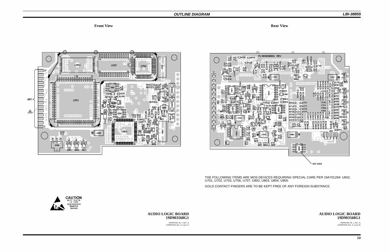
Front View Rear View
THE FOLLOWING ITEMS ARE MOS DEVICES REQUIRING SPECIAL CARE PER 19A701294: U602,U701, U702, U703, U706, U707, U802, U803, U804, U805.
GOLD CONTACT FINGERS ARE TO BE KEPT FREE OF ANY FOREIGN SUBSTANCE.
AUDIO LOGIC BOARD19D903568G1
19D903568, Sh. 1, Rev. 5)(19D903569, Rev. 4, Layer 1)
AUDIO LOGIC BOARD19D903568G1
19D903568, Sh. 1, Rev. 5)(19D903569, Rev. 4, Layer 8)
OUTLINE DIAGRAM LBI-38855
13

SCHEMATIC DIAGRAM
CONTROL ASSEMBLY19A705090G10(19C852199, Rev. 0)
LBI-38855
14
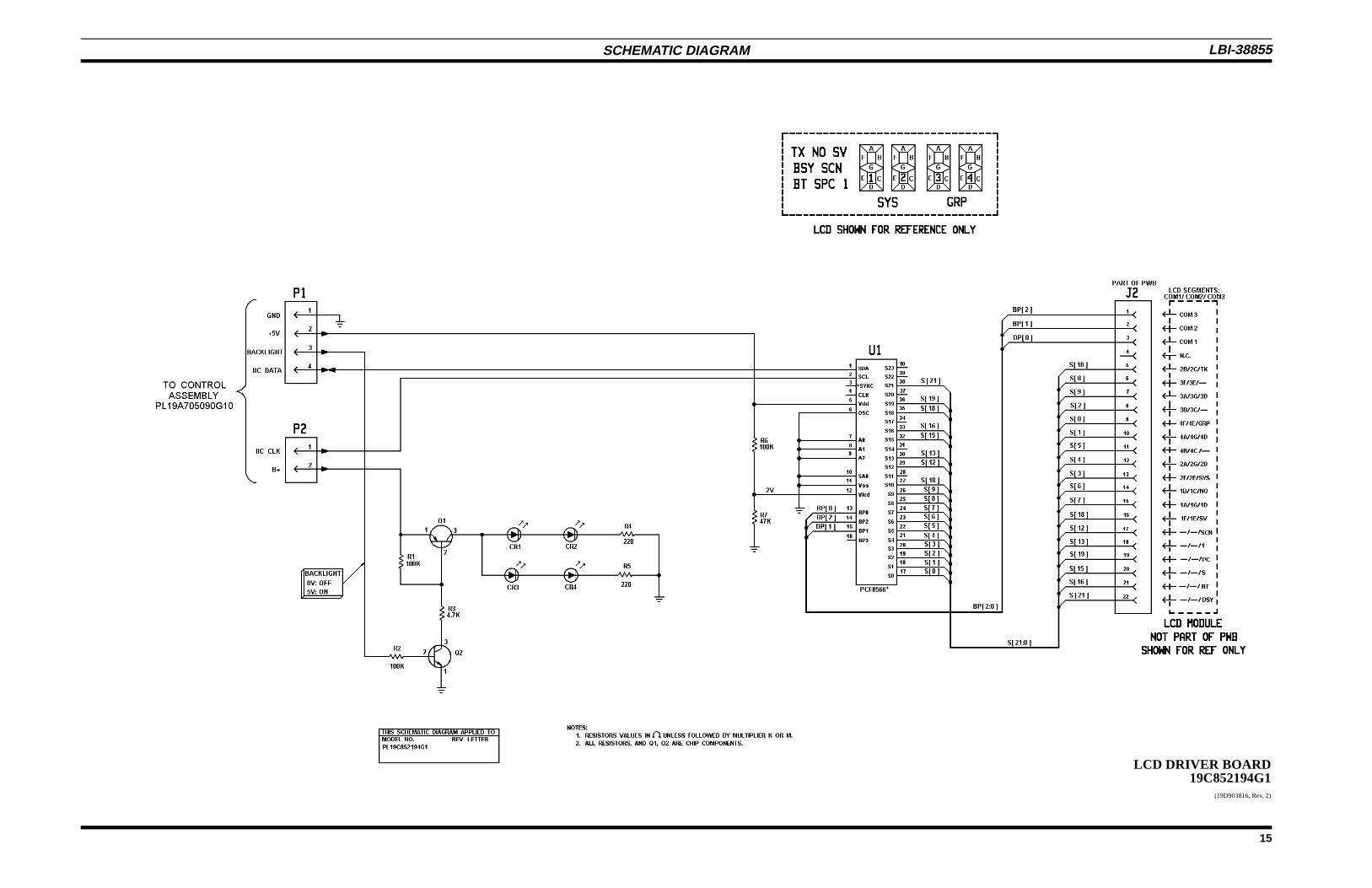
SCHEMATIC DIAGRAM
LCD DRIVER BOARD19C852194G1
(19D903816, Rev. 2)
LBI-38855
15

SCHEMATIC DIAGRAM
KEYPAD BOARD19C852173G1(19D903683, Rev. 0)
LBI-38855
16

SCHEMATIC DIAGRAM
AUDIO LOGIC BOARD19D903568G1
(19D903570 Sh. 1, Rev. 9)
LBI-38855
17

SCHEMATIC DIAGRAM
AUDIO LOGIC BOARD19D903568G1(19D903570 Sh. 2, Rev. 6)
LBI-38855
18

SCHEMATIC DIAGRAM
AUDIO LOGIC BOARD19D903568G1
(19D903570 Sh. 3, Rev. 3)
LBI-38855
19

SCHEMATIC DIAGRAM
AUDIO LOGIC BOARD19D903568G1(19D903570 Sh. 4, Rev. 7)
LBI-38855
20

SCHEMATIC DIAGRAM
AUDIO LOGIC BOARD19D903568G1
(19D903570 Sh. 5, Rev. 3)
LBI-38855
21