lan7500/lan7500i hi-speed usb 2.0 to 10/100/1000 … lan7500/lan7500i revision 1.0 (11-01-10)...
TRANSCRIPT
SMSC LAN7500/LAN7500iDATASHE
PRODUCT FEATURES
Highlights
Single Chip Hi-Speed USB 2.0 to 10/100/1000 Ethernet Controller
10/100/1000 Ethernet MAC with Full-Duplex Support
10/100/1000 Ethernet PHY with HP Auto-MDIX
Integrated USB 2.0 Hi-Speed Device Controller
Integrated USB 2.0 Hi-Speed PHY
Implements Reduced Power Operating Modes
Supports EEPROM-less Operation for Reduced BOM
NetDetach provides automatic USB attach/detach when Ethernet cable is connected/removed
Target Applications
Embedded Systems / CE Devices
Set-Top Boxes / PVR’s
Networked Printers
USB Port Replicators
Standalone USB to Ethernet Dongles
Test Instrumentation / Industrial
Key Benefits
USB Device Controller— Fully compliant with USB Specification Revision 2.0— Supports HS (480 Mbps) and FS (12 Mbps) modes— Four endpoints supported— Supports vendor specific commands— Integrated USB 2.0 PHY— Remote wakeup supported
High-Performance 10/100/1000 Ethernet Controller— Fully compliant with IEEE802.3/802.3u/802.3ab— Integrated Ethernet MAC and PHY— 10BASE-T, 100BASE-TX, and 1000BASE-T support— Full- and half-duplex capability (only full-duplex
operation at 1000Mbps)— Full-duplex flow control— Preamble generation and removal— Automatic 32-bit CRC generation and checking— 9 KB jumbo frame support— Automatic payload padding and pad removal— Loop-back modes— Supports checksum offloads (IPv4, IPv6, TCP, UDP)
— Supports Microsoft NDIS 6.2 large send offload— Supports IEEE 802.1q VLAN tagging
– Ability to add and strip IEEE 802.1q VLAN tags– VLAN tag based packet filtering (all 4096 VIDs)
LAN7500/LAN7500i
Hi-Speed USB 2.0 to 10/100/1000 Ethernet Controller
Revision 1.0 (11-01-10)ET
Datasheet
— Flexible address filtering modes– 33 exact matches (unicast or multicast)– 512-bit hash filter for multicast frames– Pass all multicast– Promiscuous unicast/multicast modes– Inverse filtering– Pass all incoming with status report
— Wakeup packet support– Perfect DA frame, wakeup frame, magic packet,
broadcast frame, IPv6 & IPv4 TCP SYN– 8 programmable 128-bit wakeup frame filters
— ARP and NS offload— PME pin support— Integrated Ethernet PHY
– Auto-negotiation– Automatic polarity detection and correction– HP Auto-MDIX support– Link status change wake-up detection
— Support for 5 status LEDs— Supports various statistical counters
Power and I/Os— Various low power modes— 12 GPIOs— Supports bus-powered and self-powered operation— Variable voltage I/O supply (2.5V/3.3V)
Miscellaneous Features— EEPROM Controller— IEEE 1149.1 (JTAG) Boundary Scan— Requires single 25 MHz crystal
Software— Windows XP/ Vista / Windows 7 Driver— Linux Driver— Win CE Driver— MAC OS Driver— EEPROM/Manufacturing Utility for Windows/DOS— PXE Support— DOS ODI Driver
Packaging— 56-pin QFN (8x8 mm) lead-free RoHS compliant
Environmental— Commercial Temperature Range (0°C to +70°C)— Industrial Temperature Range (-40°C to +85°C)

Order Numbers:
LAN7500-ABZJ for 56 pin, QFN lead-free RoHS compliant package (0 to +70°C temp range)
LAN7500i-ABZJ for 56 pin, QFN lead-free RoHS compliant package (-40 to +85°C temp range)
This product meets the halogen maximum concentration values per IEC61249-2-21
For RoHS compliance and environmental information, please visit www.smsc.com/rohs
Hi-Speed USB 2.0 to 10/100/1000 Ethernet Controller
Datasheet
Revision 1.0 (11-01-10) 2 SMSC LAN7500/LAN7500iDATASHEET
80 ARKAY DRIVE, HAUPPAUGE, NY 11788 (631) 435-6000, FAX (631) 273-3123
Copyright © 2010 SMSC or its subsidiaries. All rights reserved.
Circuit diagrams and other information relating to SMSC products are included as a means of illustrating typical applications. Consequently, complete information sufficient forconstruction purposes is not necessarily given. Although the information has been checked and is believed to be accurate, no responsibility is assumed for inaccuracies. SMSCreserves the right to make changes to specifications and product descriptions at any time without notice. Contact your local SMSC sales office to obtain the latest specificationsbefore placing your product order. The provision of this information does not convey to the purchaser of the described semiconductor devices any licenses under any patentrights or other intellectual property rights of SMSC or others. All sales are expressly conditional on your agreement to the terms and conditions of the most recently datedversion of SMSC's standard Terms of Sale Agreement dated before the date of your order (the "Terms of Sale Agreement"). The product may contain design defects or errorsknown as anomalies which may cause the product's functions to deviate from published specifications. Anomaly sheets are available upon request. SMSC products are notdesigned, intended, authorized or warranted for use in any life support or other application where product failure could cause or contribute to personal injury or severe propertydamage. Any and all such uses without prior written approval of an Officer of SMSC and further testing and/or modification will be fully at the risk of the customer. Copies ofthis document or other SMSC literature, as well as the Terms of Sale Agreement, may be obtained by visiting SMSC’s website at http://www.smsc.com. SMSC is a registeredtrademark of Standard Microsystems Corporation (“SMSC”). Product names and company names are the trademarks of their respective holders.
SMSC DISCLAIMS AND EXCLUDES ANY AND ALL WARRANTIES, INCLUDING WITHOUT LIMITATION ANY AND ALL IMPLIED WARRANTIES OF MERCHANTABILITY,FITNESS FOR A PARTICULAR PURPOSE, TITLE, AND AGAINST INFRINGEMENT AND THE LIKE, AND ANY AND ALL WARRANTIES ARISING FROM ANY COURSEOF DEALING OR USAGE OF TRADE. IN NO EVENT SHALL SMSC BE LIABLE FOR ANY DIRECT, INCIDENTAL, INDIRECT, SPECIAL, PUNITIVE, OR CONSEQUENTIALDAMAGES; OR FOR LOST DATA, PROFITS, SAVINGS OR REVENUES OF ANY KIND; REGARDLESS OF THE FORM OF ACTION, WHETHER BASED ON CONTRACT;TORT; NEGLIGENCE OF SMSC OR OTHERS; STRICT LIABILITY; BREACH OF WARRANTY; OR OTHERWISE; WHETHER OR NOT ANY REMEDY OF BUYER IS HELDTO HAVE FAILED OF ITS ESSENTIAL PURPOSE, AND WHETHER OR NOT SMSC HAS BEEN ADVISED OF THE POSSIBILITY OF SUCH DAMAGES.
Hi-Speed USB 2.0 to 10/100/1000 Ethernet Controller
Datasheet
Table of Contents
Chapter 1 Introduction . . . . . . . . . . . . . . . . . . . . . . . . . . . . . . . . . . . . . . . . . . . . . . . . . . . . . . . 71.1 Block Diagram . . . . . . . . . . . . . . . . . . . . . . . . . . . . . . . . . . . . . . . . . . . . . . . . . . . . . . . . . . . . . . . . . 7
1.1.1 Overview . . . . . . . . . . . . . . . . . . . . . . . . . . . . . . . . . . . . . . . . . . . . . . . . . . . . . . . . . . . . . . 71.1.2 USB . . . . . . . . . . . . . . . . . . . . . . . . . . . . . . . . . . . . . . . . . . . . . . . . . . . . . . . . . . . . . . . . . . 81.1.3 FIFO Controller . . . . . . . . . . . . . . . . . . . . . . . . . . . . . . . . . . . . . . . . . . . . . . . . . . . . . . . . . 81.1.4 Ethernet . . . . . . . . . . . . . . . . . . . . . . . . . . . . . . . . . . . . . . . . . . . . . . . . . . . . . . . . . . . . . . . 81.1.5 Frame Filtering . . . . . . . . . . . . . . . . . . . . . . . . . . . . . . . . . . . . . . . . . . . . . . . . . . . . . . . . . 81.1.6 Host Offloading . . . . . . . . . . . . . . . . . . . . . . . . . . . . . . . . . . . . . . . . . . . . . . . . . . . . . . . . . 91.1.7 Power Management . . . . . . . . . . . . . . . . . . . . . . . . . . . . . . . . . . . . . . . . . . . . . . . . . . . . . 91.1.8 EEPROM Controller . . . . . . . . . . . . . . . . . . . . . . . . . . . . . . . . . . . . . . . . . . . . . . . . . . . . . 91.1.9 General Purpose I/O . . . . . . . . . . . . . . . . . . . . . . . . . . . . . . . . . . . . . . . . . . . . . . . . . . . . . 91.1.10 TAP Controller . . . . . . . . . . . . . . . . . . . . . . . . . . . . . . . . . . . . . . . . . . . . . . . . . . . . . . . . . . 91.1.11 Test Features . . . . . . . . . . . . . . . . . . . . . . . . . . . . . . . . . . . . . . . . . . . . . . . . . . . . . . . . . 101.1.12 System Software . . . . . . . . . . . . . . . . . . . . . . . . . . . . . . . . . . . . . . . . . . . . . . . . . . . . . . . 10
Chapter 2 Pin Description and Configuration . . . . . . . . . . . . . . . . . . . . . . . . . . . . . . . . . . . 112.1 Pin Assignments . . . . . . . . . . . . . . . . . . . . . . . . . . . . . . . . . . . . . . . . . . . . . . . . . . . . . . . . . . . . . . . 172.2 Buffer Types . . . . . . . . . . . . . . . . . . . . . . . . . . . . . . . . . . . . . . . . . . . . . . . . . . . . . . . . . . . . . . . . . . 18
Chapter 3 EEPROM Controller (EPC) . . . . . . . . . . . . . . . . . . . . . . . . . . . . . . . . . . . . . . . . . 193.1 EEPROM Format . . . . . . . . . . . . . . . . . . . . . . . . . . . . . . . . . . . . . . . . . . . . . . . . . . . . . . . . . . . . . . 193.2 EEPROM Defaults . . . . . . . . . . . . . . . . . . . . . . . . . . . . . . . . . . . . . . . . . . . . . . . . . . . . . . . . . . . . . 243.3 EEPROM Auto-Load. . . . . . . . . . . . . . . . . . . . . . . . . . . . . . . . . . . . . . . . . . . . . . . . . . . . . . . . . . . . 243.4 An Example of EEPROM Format Interpretation . . . . . . . . . . . . . . . . . . . . . . . . . . . . . . . . . . . . . . . 25
Chapter 4 PME Operation . . . . . . . . . . . . . . . . . . . . . . . . . . . . . . . . . . . . . . . . . . . . . . . . . . . 30
Chapter 5 NetDetach Operation. . . . . . . . . . . . . . . . . . . . . . . . . . . . . . . . . . . . . . . . . . . . . . . 345.1 NetDetach. . . . . . . . . . . . . . . . . . . . . . . . . . . . . . . . . . . . . . . . . . . . . . . . . . . . . . . . . . . . . . . . . . . . 34
Chapter 6 Application Diagrams . . . . . . . . . . . . . . . . . . . . . . . . . . . . . . . . . . . . . . . . . . . . . . 366.1 Simplified Application Diagram . . . . . . . . . . . . . . . . . . . . . . . . . . . . . . . . . . . . . . . . . . . . . . . . . . . . 366.2 Power Supply & Twisted Pair Interface Diagram . . . . . . . . . . . . . . . . . . . . . . . . . . . . . . . . . . . . . . 37
Chapter 7 Operational Characteristics . . . . . . . . . . . . . . . . . . . . . . . . . . . . . . . . . . . . . . . . . 387.1 Absolute Maximum Ratings*. . . . . . . . . . . . . . . . . . . . . . . . . . . . . . . . . . . . . . . . . . . . . . . . . . . . . . 387.2 Operating Conditions** . . . . . . . . . . . . . . . . . . . . . . . . . . . . . . . . . . . . . . . . . . . . . . . . . . . . . . . . . . 397.3 Power Consumption . . . . . . . . . . . . . . . . . . . . . . . . . . . . . . . . . . . . . . . . . . . . . . . . . . . . . . . . . . . . 39
7.3.1 SUSPEND0 . . . . . . . . . . . . . . . . . . . . . . . . . . . . . . . . . . . . . . . . . . . . . . . . . . . . . . . . . . . 397.3.1.1 VDDVARIO & Magnetics = 2.5V ....................................................................................397.3.1.2 VDDVARIO & Magnetics = 3.3V ....................................................................................40
7.3.2 SUSPEND1 . . . . . . . . . . . . . . . . . . . . . . . . . . . . . . . . . . . . . . . . . . . . . . . . . . . . . . . . . . . 407.3.2.1 VDDVARIO & Magnetics = 2.5V ....................................................................................407.3.2.2 VDDVARIO & Magnetics = 3.3V ....................................................................................40
7.3.3 SUSPEND2 (Self-Powered) . . . . . . . . . . . . . . . . . . . . . . . . . . . . . . . . . . . . . . . . . . . . . . 417.3.3.1 VDDVARIO & Magnetics = 2.5V ....................................................................................417.3.3.2 VDDVARIO & Magnetics = 3.3V ....................................................................................41
7.3.4 SUSPEND2 (Bus-Powered) . . . . . . . . . . . . . . . . . . . . . . . . . . . . . . . . . . . . . . . . . . . . . . 427.3.4.1 VDDVARIO & Magnetics = 2.5V ....................................................................................427.3.4.2 VDDVARIO & Magnetics = 3.3V ....................................................................................42
7.3.5 Operational . . . . . . . . . . . . . . . . . . . . . . . . . . . . . . . . . . . . . . . . . . . . . . . . . . . . . . . . . . . 43
SMSC LAN7500/LAN7500i 3 Revision 1.0 (11-01-10)DATASHEET

Hi-Speed USB 2.0 to 10/100/1000 Ethernet Controller
Datasheet
7.3.5.1 VDDVARIO & Magnetics = 2.5V ....................................................................................437.3.5.2 VDDVARIO & Magnetics = 3.3V ....................................................................................44
7.4 DC Specifications . . . . . . . . . . . . . . . . . . . . . . . . . . . . . . . . . . . . . . . . . . . . . . . . . . . . . . . . . . . . . . 457.5 AC Specifications . . . . . . . . . . . . . . . . . . . . . . . . . . . . . . . . . . . . . . . . . . . . . . . . . . . . . . . . . . . . . . 47
7.5.1 Equivalent Test Load. . . . . . . . . . . . . . . . . . . . . . . . . . . . . . . . . . . . . . . . . . . . . . . . . . . . 477.5.2 Power Sequence Timing . . . . . . . . . . . . . . . . . . . . . . . . . . . . . . . . . . . . . . . . . . . . . . . . . 487.5.3 Power-On Reset Timing . . . . . . . . . . . . . . . . . . . . . . . . . . . . . . . . . . . . . . . . . . . . . . . . . 497.5.4 Reset Timing . . . . . . . . . . . . . . . . . . . . . . . . . . . . . . . . . . . . . . . . . . . . . . . . . . . . . . . . . . 507.5.5 EEPROM Timing . . . . . . . . . . . . . . . . . . . . . . . . . . . . . . . . . . . . . . . . . . . . . . . . . . . . . . . 517.5.6 JTAG Timing . . . . . . . . . . . . . . . . . . . . . . . . . . . . . . . . . . . . . . . . . . . . . . . . . . . . . . . . . . 52
7.6 Clock Circuit . . . . . . . . . . . . . . . . . . . . . . . . . . . . . . . . . . . . . . . . . . . . . . . . . . . . . . . . . . . . . . . . . . 53
Chapter 8 Package Outline . . . . . . . . . . . . . . . . . . . . . . . . . . . . . . . . . . . . . . . . . . . . . . . . . . . 54
Chapter 9 Revision History. . . . . . . . . . . . . . . . . . . . . . . . . . . . . . . . . . . . . . . . . . . . . . . . . . . 56
Revision 1.0 (11-01-10) 4 SMSC LAN7500/LAN7500iDATASHEET
Hi-Speed USB 2.0 to 10/100/1000 Ethernet Controller
Datasheet
SMSC LAN7500/LAN7500i 5 Revision 1.0 (11-01-10)DATASHEET
List of Figures
Figure 1.1 LAN7500/LAN7500i System Diagram . . . . . . . . . . . . . . . . . . . . . . . . . . . . . . . . . . . . . . . . . . . 7Figure 2.1 LAN7500/LAN7500i 56-QFN Pin Assignments (TOP VIEW). . . . . . . . . . . . . . . . . . . . . . . . . 11Figure 4.1 Typical Application . . . . . . . . . . . . . . . . . . . . . . . . . . . . . . . . . . . . . . . . . . . . . . . . . . . . . . . . . 30Figure 4.2 PME Operation. . . . . . . . . . . . . . . . . . . . . . . . . . . . . . . . . . . . . . . . . . . . . . . . . . . . . . . . . . . . 33Figure 5.1 LAN7500/LAN7500i Detach . . . . . . . . . . . . . . . . . . . . . . . . . . . . . . . . . . . . . . . . . . . . . . . . . . 34Figure 5.2 LAN7500/LAN7500i Attach . . . . . . . . . . . . . . . . . . . . . . . . . . . . . . . . . . . . . . . . . . . . . . . . . . 35Figure 6.1 Simplified Application Diagram . . . . . . . . . . . . . . . . . . . . . . . . . . . . . . . . . . . . . . . . . . . . . . . 36Figure 6.2 Power Supply & Twisted Pair Interface Diagram . . . . . . . . . . . . . . . . . . . . . . . . . . . . . . . . . . 37Figure 7.1 Output Equivalent Test Load . . . . . . . . . . . . . . . . . . . . . . . . . . . . . . . . . . . . . . . . . . . . . . . . . 47Figure 7.2 Power Sequence Timing . . . . . . . . . . . . . . . . . . . . . . . . . . . . . . . . . . . . . . . . . . . . . . . . . . . . 48Figure 7.3 nRESET Power-On Timing . . . . . . . . . . . . . . . . . . . . . . . . . . . . . . . . . . . . . . . . . . . . . . . . . . 49Figure 7.4 nRESET Timing . . . . . . . . . . . . . . . . . . . . . . . . . . . . . . . . . . . . . . . . . . . . . . . . . . . . . . . . . . . 50Figure 7.5 EEPROM Timing . . . . . . . . . . . . . . . . . . . . . . . . . . . . . . . . . . . . . . . . . . . . . . . . . . . . . . . . . . 51Figure 7.6 JTAG Timing . . . . . . . . . . . . . . . . . . . . . . . . . . . . . . . . . . . . . . . . . . . . . . . . . . . . . . . . . . . . . 52Figure 8.1 LAN7500/LAN7500i 56-QFN Package. . . . . . . . . . . . . . . . . . . . . . . . . . . . . . . . . . . . . . . . . . 54Figure 8.2 LAN7500/LAN7500i 56-QFN Recommended PCB Land Pattern . . . . . . . . . . . . . . . . . . . . . 55
Hi-Speed USB 2.0 to 10/100/1000 Ethernet Controller
Datasheet
Revision 1.0 (11-01-10) 6 SMSC LAN7500/LAN7500iDATASHEET
List Of Tables
Table 1.1 IEEE 1149.1 Op Codes . . . . . . . . . . . . . . . . . . . . . . . . . . . . . . . . . . . . . . . . . . . . . . . . . . . . . . 10Table 2.1 GPIO Pins . . . . . . . . . . . . . . . . . . . . . . . . . . . . . . . . . . . . . . . . . . . . . . . . . . . . . . . . . . . . . . . . 12Table 2.2 EEPROM Pins . . . . . . . . . . . . . . . . . . . . . . . . . . . . . . . . . . . . . . . . . . . . . . . . . . . . . . . . . . . . . 13Table 2.3 JTAG Pins . . . . . . . . . . . . . . . . . . . . . . . . . . . . . . . . . . . . . . . . . . . . . . . . . . . . . . . . . . . . . . . . 14Table 2.4 USB Pins . . . . . . . . . . . . . . . . . . . . . . . . . . . . . . . . . . . . . . . . . . . . . . . . . . . . . . . . . . . . . . . . . 14Table 2.5 Ethernet PHY Pins. . . . . . . . . . . . . . . . . . . . . . . . . . . . . . . . . . . . . . . . . . . . . . . . . . . . . . . . . . 15Table 2.6 Miscellaneous Pins . . . . . . . . . . . . . . . . . . . . . . . . . . . . . . . . . . . . . . . . . . . . . . . . . . . . . . . . . 16Table 2.7 I/O Power Pins, Core Power Pins, and Ground Pad . . . . . . . . . . . . . . . . . . . . . . . . . . . . . . . . 16Table 2.8 56-QFN Package Pin Assignments . . . . . . . . . . . . . . . . . . . . . . . . . . . . . . . . . . . . . . . . . . . . . 17Table 2.9 Buffer Types . . . . . . . . . . . . . . . . . . . . . . . . . . . . . . . . . . . . . . . . . . . . . . . . . . . . . . . . . . . . . . 18Table 3.1 EEPROM Format. . . . . . . . . . . . . . . . . . . . . . . . . . . . . . . . . . . . . . . . . . . . . . . . . . . . . . . . . . . 19Table 3.2 Configuration Flags 0. . . . . . . . . . . . . . . . . . . . . . . . . . . . . . . . . . . . . . . . . . . . . . . . . . . . . . . . 21Table 3.3 Configuration Flags 1. . . . . . . . . . . . . . . . . . . . . . . . . . . . . . . . . . . . . . . . . . . . . . . . . . . . . . . . 22Table 3.4 GPIO PME Flags . . . . . . . . . . . . . . . . . . . . . . . . . . . . . . . . . . . . . . . . . . . . . . . . . . . . . . . . . . . 23Table 3.5 EEPROM Defaults . . . . . . . . . . . . . . . . . . . . . . . . . . . . . . . . . . . . . . . . . . . . . . . . . . . . . . . . . . 24Table 3.6 Dump of EEPROM Memory. . . . . . . . . . . . . . . . . . . . . . . . . . . . . . . . . . . . . . . . . . . . . . . . . . . 25Table 3.7 EEPROM Example - 256 Byte EEPROM . . . . . . . . . . . . . . . . . . . . . . . . . . . . . . . . . . . . . . . . 26Table 7.1 SUSPEND0 Current & Power (VDDVARIO & Magnetics = 2.5V) . . . . . . . . . . . . . . . . . . . . . . 39Table 7.2 SUSPEND0 Current & Power (VDDVARIO & Magnetics = 3.3V) . . . . . . . . . . . . . . . . . . . . . . 40Table 7.3 SUSPEND1 Current & Power (VDDVARIO & Magnetics = 2.5V) . . . . . . . . . . . . . . . . . . . . . . 40Table 7.4 SUSPEND1 Current & Power (VDDVARIO & Magnetics = 3.3V) . . . . . . . . . . . . . . . . . . . . . . 40Table 7.5 SUSPEND2 (Self-Powered) Current & Power (VDDVARIO & Magnetics = 2.5V) . . . . . . . . . 41Table 7.6 SUSPEND2 (Self-Powered) Current & Power (VDDVARIO & Magnetics = 3.3V) . . . . . . . . . 41Table 7.7 SUSPEND2 (Bus-Powered) Current & Power (VDDVARIO & Magnetics = 2.5V) . . . . . . . . . 42Table 7.8 SUSPEND2 (Bus-Powered) Current & Power (VDDVARIO & Magnetics = 3.3V) . . . . . . . . . 42Table 7.9 Operational Current & Power (VDDVARIO & Magnetics = 2.5V) . . . . . . . . . . . . . . . . . . . . . . 43Table 7.10 Operational Current & Power (VDDVARIO & Magnetics = 3.3V) . . . . . . . . . . . . . . . . . . . . . . 44Table 7.11 I/O Buffer Characteristics. . . . . . . . . . . . . . . . . . . . . . . . . . . . . . . . . . . . . . . . . . . . . . . . . . . . . 45Table 7.12 1000BASE-T Transceiver Characteristics . . . . . . . . . . . . . . . . . . . . . . . . . . . . . . . . . . . . . . . . 46Table 7.13 100BASE-TX Transceiver Characteristics. . . . . . . . . . . . . . . . . . . . . . . . . . . . . . . . . . . . . . . . 46Table 7.14 10BASE-T Transceiver Characteristics . . . . . . . . . . . . . . . . . . . . . . . . . . . . . . . . . . . . . . . . . . 47Table 7.15 Power Sequence Timing Values . . . . . . . . . . . . . . . . . . . . . . . . . . . . . . . . . . . . . . . . . . . . . . . 48Table 7.16 nRESET Power-On Timing Values . . . . . . . . . . . . . . . . . . . . . . . . . . . . . . . . . . . . . . . . . . . . . 49Table 7.17 nRESET Timing Values . . . . . . . . . . . . . . . . . . . . . . . . . . . . . . . . . . . . . . . . . . . . . . . . . . . . . . 50Table 7.18 EEPROM Timing Values . . . . . . . . . . . . . . . . . . . . . . . . . . . . . . . . . . . . . . . . . . . . . . . . . . . . . 51Table 7.19 JTAG Timing Values . . . . . . . . . . . . . . . . . . . . . . . . . . . . . . . . . . . . . . . . . . . . . . . . . . . . . . . . 52Table 7.20 LAN7500/LAN7500i Crystal Specifications . . . . . . . . . . . . . . . . . . . . . . . . . . . . . . . . . . . . . . . 53Table 8.1 LAN7500/LAN7500i 56-QFN Dimensions . . . . . . . . . . . . . . . . . . . . . . . . . . . . . . . . . . . . . . . . 54Table 9.1 Customer Revision History . . . . . . . . . . . . . . . . . . . . . . . . . . . . . . . . . . . . . . . . . . . . . . . . . . . 56

Hi-Speed USB 2.0 to 10/100/1000 Ethernet Controller
Datasheet
Chapter 1 Introduction
1.1 Block Diagram
1.1.1 Overview
The LAN7500/LAN7500i is a high performance Hi-Speed USB 2.0 to 10/100/1000 Ethernet controller.With applications ranging from embedded systems, set-top boxes, and PVR’s, to USB port replicators,USB to Ethernet dongles, and test instrumentation, the device is a high performance and costcompetitive USB to Ethernet connectivity solution.
The LAN7500/LAN7500i contains an integrated 10/100/1000 Ethernet MAC and PHY, Filtering Engine,USB PHY, Hi-Speed USB 2.0 device controller, TAP controller, EEPROM controller, and a FIFOcontroller with a total of 32 KB of internal packet buffering.
The internal USB 2.0 device controller and USB PHY are compliant with the USB 2.0 Hi-Speedstandard. The device implements Control, Interrupt, Bulk-in, and Bulk-out USB Endpoints.
The Ethernet controller supports auto-negotiation, auto-polarity correction, HP Auto-MDIX, and iscompliant with the IEEE 802.3, IEEE 802.3u, IEEE 802.3ab standards. ARP and NS offload is alsosupported.
Multiple power management features are provided, including various low power modes and "MagicPacket", "Wake On LAN", and "Link Status Change" wake events. These wake events can beprogrammed to initiate a USB remote wakeup.
An internal EEPROM controller exists to load various USB configuration information and the deviceMAC address. The integrated IEEE 1149.1 compliant TAP controller provides boundary scan via JTAG.
Figure 1.1 LAN7500/LAN7500i System Diagram
TAP Controller EEPROM
Controller
USB 2.0 Device
Controller
SRAM
EthernetPHY
10/100/1000
EthernetMAC
FIFO Controller
USBPHY
LAN7500/LAN7500i
Ethernet
EEPROM
JTAG
USBReceive Filtering Engine
SMSC LAN7500/LAN7500i 7 Revision 1.0 (11-01-10)DATASHEET
Hi-Speed USB 2.0 to 10/100/1000 Ethernet Controller
Datasheet
1.1.2 USB
The USB portion of the LAN7500/LAN7500i integrates a Hi-Speed USB 2.0 device controller and USBPHY.
The USB device controller contains a USB low-level protocol interpreter which implements the USBbus protocol, packet generation/extraction, PID/Device ID parsing, and CRC coding/decoding, withautonomous error handling. The USB device controller is capable of operating in USB 2.0 Hi-Speedand Full-Speed compliant modes and contains autonomous protocol handling functions such ashandling of suspend/resume/reset conditions, remote wakeup, and stall condition clearing on Setuppackets. The USB device controller also autonomously handles error conditions such as retry for CRCand data toggle errors, and generates NYET, STALL, ACK and NACK handshake responses,depending on the endpoint buffer status.
The LAN7500/LAN7500i implements four USB endpoints: Control, Interrupt, Bulk-in, and Bulk-out. TheBulk-in and Bulk-out Endpoints allow for Ethernet reception and transmission respectively.Implementation of vendor-specific commands allows for efficient statistics gathering and access to thedevice’s system control and status registers.
1.1.3 FIFO Controller
The FIFO controller uses two internal SRAMs to buffer RX and TX traffic. Bulk-Out packets from theUSB controller are directly stored into the TX buffer. The FIFO Controller is responsible for extractingEthernet frames from the USB packet data and passing the frames to the MAC. Received EthernetFrames are filtered by the Receive Filtering Engine and frames meeting the filtering constraints arestored into the RX buffer and become the basis for bulk-in packets.
1.1.4 Ethernet
The LAN7500/LAN7500i integrates an IEEE 802.3/802.3u/802.3ab compliant PHY for twisted pairEthernet applications and a 10/100/1000 Ethernet Media Access Controller (MAC).
The PHY can be configured for 1000 Mbps (1000BASE-T), 100 Mbps (100BASE-TX) or 10 Mbps(10BASE-T) operation in Full-Duplex mode. It can be configured for 100 Mbps or 10 Mbps operationin Half Duplex mode. The PHY block includes auto-negotiation, auto-polarity correction, and Auto-MDIX. Minimal external components are required for the utilization of the Integrated PHY.
The Ethernet MAC/PHY supports numerous power management wakeup features, including “MagicPacket”, “Wake on LAN”, and “Link Status Change”. Microsoft NDIS 6.2 and Windows 7 compliant ARPand NS offload support is also provided.The device will respond to an NS or ARP request bygenerating and transmitting a response. When received in a SUSPEND state, an NS or ARP requestwill not result in the generation of a wake event. Additionally, five status LEDs are supported.
1.1.5 Frame Filtering
The LAN7500/LAN7500i Receive Filtering Engine performs frame filtering. It supports 33 perfectaddress filters. These can be used to filter either the Ethernet source address or destination address.Additional address filtering is available via a 512-bit hash filter. The hash filter can perform unicast ormulticast filtering.
VLAN tagged frames can be filtered via the VLAN ID. A 4096-bit table exists to support all possibleVLAN IDs. The VLAN type can be programmed. Double tagging is supported.
Revision 1.0 (11-01-10) 8 SMSC LAN7500/LAN7500iDATASHEET
Hi-Speed USB 2.0 to 10/100/1000 Ethernet Controller
Datasheet
1.1.6 Host Offloading
The LAN7500/LAN7500i supports a variety of TCP/UDP/IP checksum offloads to reduce the burdenon the host processor. For Ethernet receive frames, the device can be configured to validate the IPchecksum and UDP/TCP checksum. Both IPv4 and IPv6 packets are supported. A raw checksumacross the layer 3 packet can also be provided.
For Ethernet transmitted frames, the device can be configured to calculate the IP checksum andUDP/TCP checksum. Additionally, Large Send Offload (LSO) is supported to further reduce host CPUloading.
1.1.7 Power Management
The LAN7500/LAN7500i features four variations of USB suspend: SUSPEND0, SUSPEND1,SUSPEND2, and SUSPEND3. These modes allow the application to select the ideal balance of remotewakeup functionality and power consumption.
SUSPEND0: Supports GPIO, “Wake On LAN”, “Magic Packet”, and “PHY Link Up” remote wakeup events. It, however, consumes the most power.
SUSPEND1: Supports GPIO and “Link Status Change” for remote wakeup events. This suspend state consumes less power than SUSPEND0.
SUSPEND2: Supports only GPIO assertion for a remote wakeup event. This is the default suspend mode for the device.
SUSPEND3: Supports GPIO, “Good Packet”, and “PHY Link Up” remote wakeup events. A “Good Packet” is a received frame that is free of errors and passes certain filtering constraints independent of those imposed on “Wake On LAN” and “Magic Packet” frames. This suspend state consumes power at a level similar to the NORMAL state, however, it allows for power savings in the Host CPU, which greatly exceeds that of the LAN7500/LAN7500i. The driver may place the device in this state after prolonged periods of not receiving any Ethernet traffic.
1.1.8 EEPROM Controller
The LAN7500/LAN7500i contains an EEPROM controller for connection to an external EEPROM. Thisallows for the automatic loading of static configuration data upon pin reset, or software reset. TheEEPROM can be configured to load USB descriptors, USB device configuration, and MAC address.
Custom operation without EEPROM is also provided.
1.1.9 General Purpose I/O
Twelve GPIOs are supported. All GPIOs can serve as remote wakeup events when theLAN7500/LAN7500i is in a suspended state.
1.1.10 TAP Controller
IEEE 1149.1 compliant TAP Controller supports boundary scan and various test modes.
The device includes an integrated JTAG boundary-scan test port for board-level testing. The interfaceconsists of four pins (TDO, TDI, TCK and TMS) and includes a state machine, data register array, andan instruction register. The JTAG pins are described in Table 2.3, “JTAG Pins,” on page 14. The JTAGinterface conforms to the IEEE Standard 1149.1 - 1990 Standard Test Access Port (TAP) andBoundary-Scan Architecture.
All input and output data is synchronous to the TCK test clock input. TAP input signals TMS and TDIare clocked into the test logic on the rising edge of TCK, while the output signal TDO is clocked onthe falling edge.
The JTAG logic is reset when the TMS and TDI pins are high for five TCK periods.
SMSC LAN7500/LAN7500i 9 Revision 1.0 (11-01-10)DATASHEET
Hi-Speed USB 2.0 to 10/100/1000 Ethernet Controller
Datasheet
The implemented IEEE 1149.1 instructions and their op codes are shown in Table 1.1.
Note: All digital I/O pins support IEEE 1149.1 operation. Analog pins and the XO pin do not supportIEEE 1149.1 operation.
1.1.11 Test Features
Read/Write access to internal SRAMs is provided via the devices registers. JTAG based USB BIST isavailable.
1.1.12 System Software
LAN7500/LAN7500i software drivers are available for the following operating systems:
Windows XP/ Vista/ Windows 7
Win CE
Linux
MAC OS
DOS ODI
In addition, an EEPROM programming utility is available for configuring the external EEPROM. PXESupport is also available.
Table 1.1 IEEE 1149.1 Op Codes
INSTRUCTION OP CODE COMMENT
Bypass 111 Mandatory Instruction
Sample/Preload 010 Mandatory Instruction
EXTEST 000 Mandatory Instruction
Clamp 011 Optional Instruction
HIGHZ 100 Optional Instruction
IDCODE 001 Optional Instruction
Revision 1.0 (11-01-10) 10 SMSC LAN7500/LAN7500iDATASHEET
Hi-Speed USB 2.0 to 10/100/1000 Ethernet Controller
Datasheet
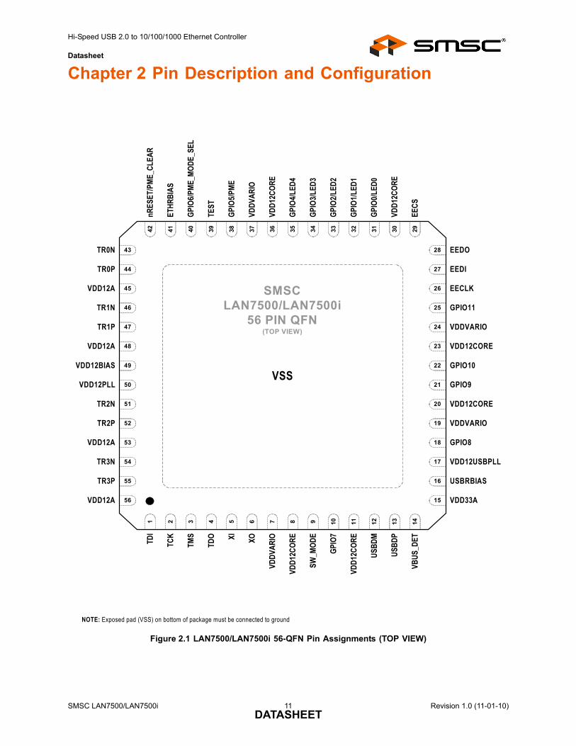
Chapter 2 Pin Description and Configuration
Figure 2.1 LAN7500/LAN7500i 56-QFN Pin Assignments (TOP VIEW)
VSS
NOTE: Exposed pad (VSS) on bottom of package must be connected to ground
SMSCLAN7500/LAN7500i
56 PIN QFN(TOP VIEW)
TR0N
nRES
ET/P
ME_
CLE
AR
EEDO
VBU
S_D
ET
1 2 3 4 5 6 7 8 9 10 11 12 13 14
15
16
17
18
19
20
21
22
23
24
25
26
27
28
42 41 40 39 38 37 36 35 34 33 32 31 30 29
56
55
54
53
52
51
50
49
48
47
46
45
44
43
USB
DP
USB
DM
VDD
12C
OR
E
GPI
O7
SW_M
OD
E
VDD
12C
OR
E
VDD
VAR
IOXOXI
TDO
TMS
TCK
TDI
ETH
RB
IAS
GPI
O6/
PME_
MO
DE_
SEL
TEST
GPI
O5/
PME
VDD
VAR
IO
VDD
12C
OR
E
GPI
O4/
LED
4
GPI
O3/
LED
3
GPI
O2/
LED
2
GPI
O1/
LED
1
GPI
O0/
LED
0
VDD
12C
OR
E
EEC
S
TR0P
VDD12A
TR1N
TR1P
VDD12A
VDD12BIAS
VDD12PLL
TR2N
TR2P
VDD12A
TR3N
TR3P
VDD12A
EEDI
EECLK
GPIO11
VDDVARIO
VDD12CORE
GPIO10
GPIO9
VDD12CORE
VDDVARIO
GPIO8
VDD12USBPLL
USBRBIAS
VDD33A
SMSC LAN7500/LAN7500i 11 Revision 1.0 (11-01-10)DATASHEET
Hi-Speed USB 2.0 to 10/100/1000 Ethernet Controller
Datasheet
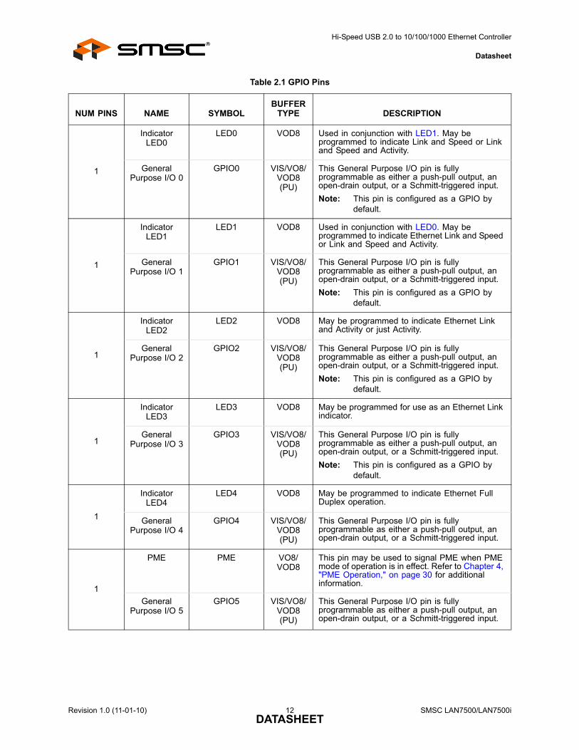
Table 2.1 GPIO Pins
NUM PINS NAME SYMBOLBUFFER
TYPE DESCRIPTION
1
Indicator LED0
LED0 VOD8 Used in conjunction with LED1. May be programmed to indicate Link and Speed or Link and Speed and Activity.
General Purpose I/O 0
GPIO0 VIS/VO8/VOD8(PU)
This General Purpose I/O pin is fully programmable as either a push-pull output, an open-drain output, or a Schmitt-triggered input.
Note: This pin is configured as a GPIO by default.
1
Indicator LED1
LED1 VOD8 Used in conjunction with LED0. May be programmed to indicate Ethernet Link and Speed or Link and Speed and Activity.
General Purpose I/O 1
GPIO1 VIS/VO8/VOD8(PU)
This General Purpose I/O pin is fully programmable as either a push-pull output, an open-drain output, or a Schmitt-triggered input.
Note: This pin is configured as a GPIO by default.
1
Indicator LED2
LED2 VOD8 May be programmed to indicate Ethernet Link and Activity or just Activity.
General Purpose I/O 2
GPIO2 VIS/VO8/VOD8(PU)
This General Purpose I/O pin is fully programmable as either a push-pull output, an open-drain output, or a Schmitt-triggered input.
Note: This pin is configured as a GPIO by default.
1
Indicator LED3
LED3 VOD8 May be programmed for use as an Ethernet Link indicator.
General Purpose I/O 3
GPIO3 VIS/VO8/VOD8(PU)
This General Purpose I/O pin is fully programmable as either a push-pull output, an open-drain output, or a Schmitt-triggered input.
Note: This pin is configured as a GPIO by default.
1
Indicator LED4
LED4 VOD8 May be programmed to indicate Ethernet Full Duplex operation.
General Purpose I/O 4
GPIO4 VIS/VO8/VOD8(PU)
This General Purpose I/O pin is fully programmable as either a push-pull output, an open-drain output, or a Schmitt-triggered input.
1
PME PME VO8/VOD8
This pin may be used to signal PME when PME mode of operation is in effect. Refer to Chapter 4, "PME Operation," on page 30 for additional information.
General Purpose I/O 5
GPIO5 VIS/VO8/VOD8(PU)
This General Purpose I/O pin is fully programmable as either a push-pull output, an open-drain output, or a Schmitt-triggered input.
Revision 1.0 (11-01-10) 12 SMSC LAN7500/LAN7500iDATASHEET
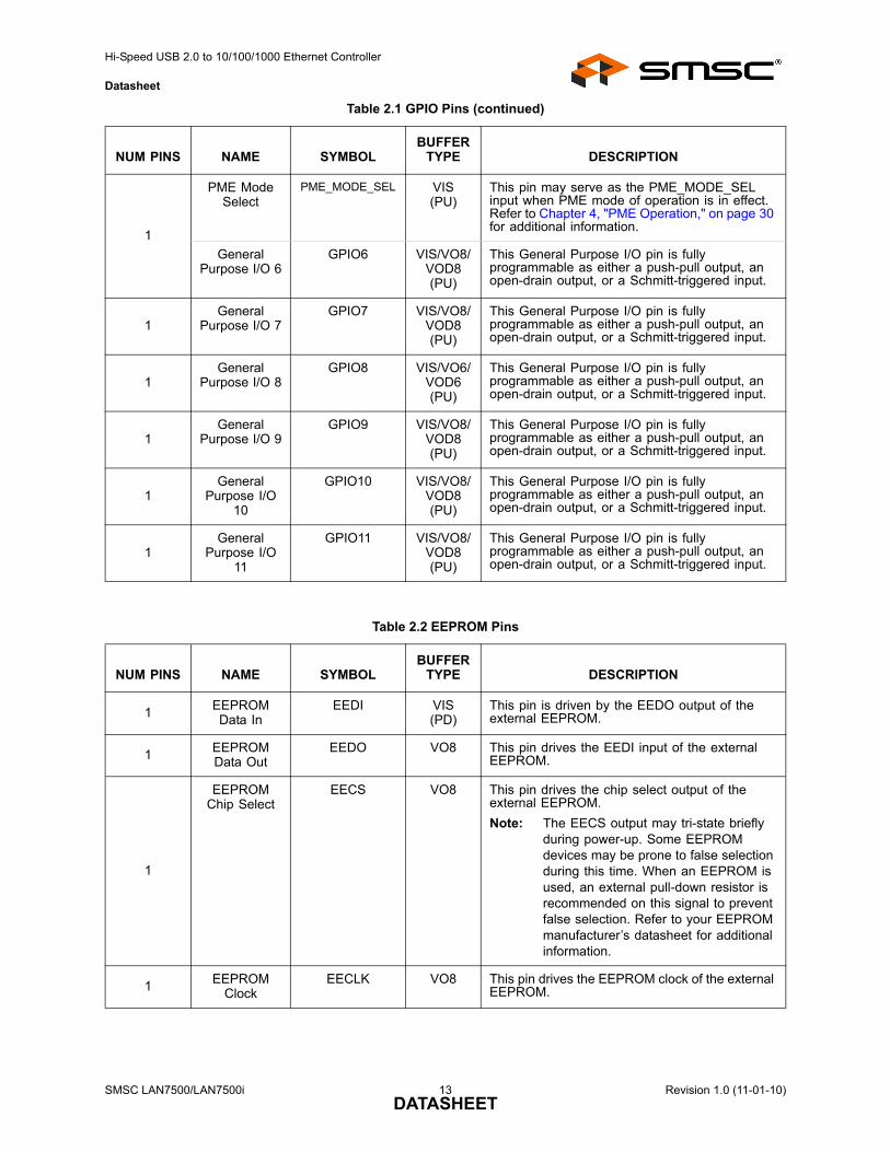
Hi-Speed USB 2.0 to 10/100/1000 Ethernet Controller
Datasheet
1
PME Mode Select
PME_MODE_SEL VIS(PU)
This pin may serve as the PME_MODE_SEL input when PME mode of operation is in effect. Refer to Chapter 4, "PME Operation," on page 30 for additional information.
General Purpose I/O 6
GPIO6 VIS/VO8/VOD8(PU)
This General Purpose I/O pin is fully programmable as either a push-pull output, an open-drain output, or a Schmitt-triggered input.
1General
Purpose I/O 7GPIO7 VIS/VO8/
VOD8(PU)
This General Purpose I/O pin is fully programmable as either a push-pull output, an open-drain output, or a Schmitt-triggered input.
1General
Purpose I/O 8GPIO8 VIS/VO6/
VOD6(PU)
This General Purpose I/O pin is fully programmable as either a push-pull output, an open-drain output, or a Schmitt-triggered input.
1General
Purpose I/O 9GPIO9 VIS/VO8/
VOD8(PU)
This General Purpose I/O pin is fully programmable as either a push-pull output, an open-drain output, or a Schmitt-triggered input.
1General
Purpose I/O 10
GPIO10 VIS/VO8/VOD8(PU)
This General Purpose I/O pin is fully programmable as either a push-pull output, an open-drain output, or a Schmitt-triggered input.
1General
Purpose I/O 11
GPIO11 VIS/VO8/VOD8(PU)
This General Purpose I/O pin is fully programmable as either a push-pull output, an open-drain output, or a Schmitt-triggered input.
Table 2.2 EEPROM Pins
NUM PINS NAME SYMBOLBUFFER
TYPE DESCRIPTION
1EEPROM Data In
EEDI VIS(PD)
This pin is driven by the EEDO output of the external EEPROM.
1 EEPROM Data Out
EEDO VO8 This pin drives the EEDI input of the external EEPROM.
1
EEPROM Chip Select
EECS VO8 This pin drives the chip select output of the external EEPROM.
Note: The EECS output may tri-state briefly during power-up. Some EEPROM devices may be prone to false selection during this time. When an EEPROM is used, an external pull-down resistor is recommended on this signal to prevent false selection. Refer to your EEPROM manufacturer’s datasheet for additional information.
1 EEPROM Clock
EECLK VO8 This pin drives the EEPROM clock of the external EEPROM.
Table 2.1 GPIO Pins (continued)
NUM PINS NAME SYMBOLBUFFER
TYPE DESCRIPTION
SMSC LAN7500/LAN7500i 13 Revision 1.0 (11-01-10)DATASHEET
Hi-Speed USB 2.0 to 10/100/1000 Ethernet Controller
Datasheet
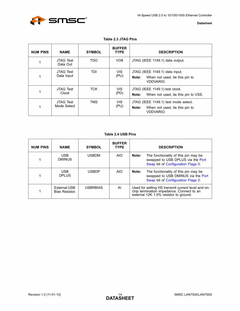
Table 2.3 JTAG Pins
NUM PINS NAME SYMBOLBUFFER
TYPE DESCRIPTION
1 JTAG Test Data Out
TDO VO8 JTAG (IEEE 1149.1) data output.
1JTAG Test Data Input
TDI VIS(PU)
JTAG (IEEE 1149.1) data input.
Note: When not used, tie this pin to VDDVARIO.
1JTAG Test
ClockTCK VIS
(PD)JTAG (IEEE 1149.1) test clock.
Note: When not used, tie this pin to VSS.
1JTAG Test
Mode SelectTMS VIS
(PU)JTAG (IEEE 1149.1) test mode select.
Note: When not used, tie this pin to VDDVARIO.
Table 2.4 USB Pins
NUM PINS NAME SYMBOLBUFFER
TYPE DESCRIPTION
1USB
DMINUSUSBDM AIO Note: The functionality of this pin may be
swapped to USB DPLUS via the Port Swap bit of Configuration Flags 0.
1USB
DPLUSUSBDP AIO Note: The functionality of this pin may be
swapped to USB DMINUS via the Port Swap bit of Configuration Flags 0.
1External USB Bias Resistor.
USBRBIAS AI Used for setting HS transmit current level and on-chip termination impedance. Connect to an external 12K 1.0% resistor to ground.
Revision 1.0 (11-01-10) 14 SMSC LAN7500/LAN7500iDATASHEET
Hi-Speed USB 2.0 to 10/100/1000 Ethernet Controller
Datasheet
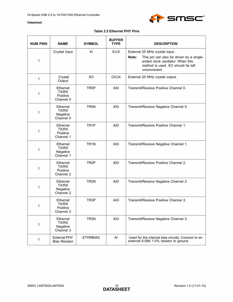
Table 2.5 Ethernet PHY Pins
NUM PINS NAME SYMBOLBUFFER
TYPE DESCRIPTION
1
Crystal Input XI ICLK External 25 MHz crystal input.
Note: This pin can also be driven by a single-ended clock oscillator. When this method is used, XO should be left unconnected
1 Crystal Output
XO OCLK External 25 MHz crystal output.
1
Ethernet TX/RX Positive
Channel 0
TR0P AIO Transmit/Receive Positive Channel 0.
1
Ethernet TX/RX
Negative Channel 0
TR0N AIO Transmit/Receive Negative Channel 0.
1
Ethernet TX/RX Positive
Channel 1
TR1P AIO Transmit/Receive Positive Channel 1.
1
Ethernet TX/RX
Negative Channel 1
TR1N AIO Transmit/Receive Negative Channel 1.
1
Ethernet TX/RX Positive
Channel 2
TR2P AIO Transmit/Receive Positive Channel 2.
1
Ethernet TX/RX
Negative Channel 2
TR2N AIO Transmit/Receive Negative Channel 2.
1
Ethernet TX/RX Positive
Channel 3
TR3P AIO Transmit/Receive Positive Channel 3.
1
Ethernet TX/RX
Negative Channel 3
TR3N AIO Transmit/Receive Negative Channel 3.
1External PHY Bias Resistor
ETHRBIAS AI Used for the internal bias circuits. Connect to an external 8.06K 1.0% resistor to ground.
SMSC LAN7500/LAN7500i 15 Revision 1.0 (11-01-10)DATASHEET
Hi-Speed USB 2.0 to 10/100/1000 Ethernet Controller
Datasheet
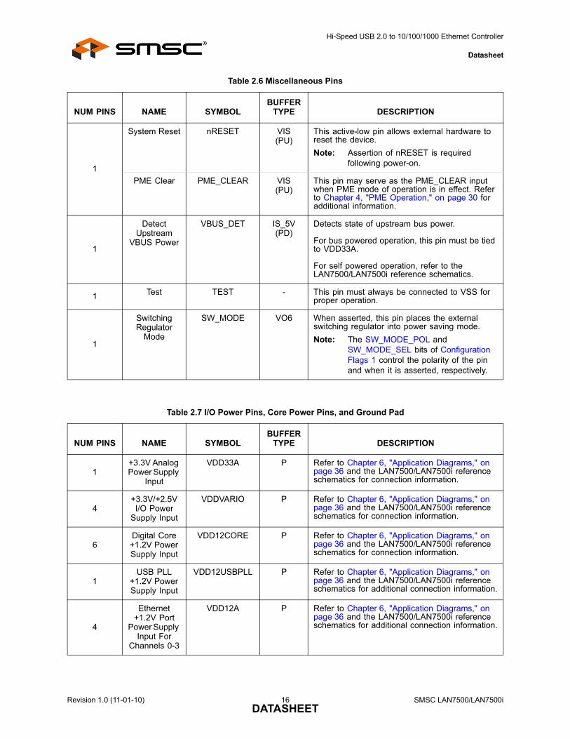
Table 2.6 Miscellaneous Pins
NUM PINS NAME SYMBOLBUFFER
TYPE DESCRIPTION
1
System Reset nRESET VIS(PU)
This active-low pin allows external hardware to reset the device.
Note: Assertion of nRESET is required following power-on.
PME Clear PME_CLEAR VIS(PU)
This pin may serve as the PME_CLEAR input when PME mode of operation is in effect. Refer to Chapter 4, "PME Operation," on page 30 for additional information.
1
Detect Upstream
VBUS Power
VBUS_DET IS_5V(PD)
Detects state of upstream bus power.
For bus powered operation, this pin must be tied to VDD33A.
For self powered operation, refer to the LAN7500/LAN7500i reference schematics.
1 Test TEST - This pin must always be connected to VSS for proper operation.
1
Switching Regulator
Mode
SW_MODE VO6 When asserted, this pin places the external switching regulator into power saving mode.
Note: The SW_MODE_POL and SW_MODE_SEL bits of Configuration Flags 1 control the polarity of the pin and when it is asserted, respectively.
Table 2.7 I/O Power Pins, Core Power Pins, and Ground Pad
NUM PINS NAME SYMBOLBUFFER
TYPE DESCRIPTION
1+3.3V Analog Power Supply
Input
VDD33A P Refer to Chapter 6, "Application Diagrams," on page 36 and the LAN7500/LAN7500i reference schematics for connection information.
4+3.3V/+2.5VI/O Power
Supply Input
VDDVARIO P Refer to Chapter 6, "Application Diagrams," on page 36 and the LAN7500/LAN7500i reference schematics for connection information.
6Digital Core +1.2V Power Supply Input
VDD12CORE P Refer to Chapter 6, "Application Diagrams," on page 36 and the LAN7500/LAN7500i reference schematics for connection information.
1USB PLL
+1.2V Power Supply Input
VDD12USBPLL P Refer to Chapter 6, "Application Diagrams," on page 36 and the LAN7500/LAN7500i reference schematics for additional connection information.
4
Ethernet +1.2V Port
Power Supply Input For
Channels 0-3
VDD12A P Refer to Chapter 6, "Application Diagrams," on page 36 and the LAN7500/LAN7500i reference schematics for additional connection information.
Revision 1.0 (11-01-10) 16 SMSC LAN7500/LAN7500iDATASHEET
Hi-Speed USB 2.0 to 10/100/1000 Ethernet Controller
Datasheet
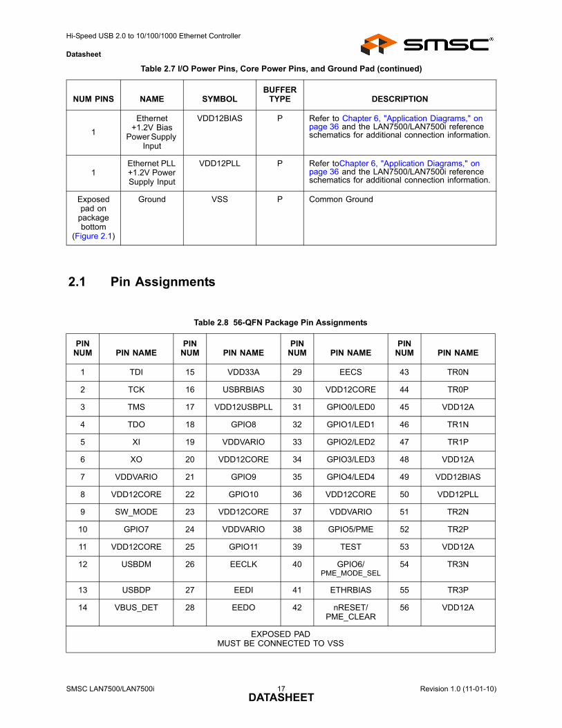
2.1 Pin Assignments
1
Ethernet +1.2V Bias
Power Supply Input
VDD12BIAS P Refer to Chapter 6, "Application Diagrams," on page 36 and the LAN7500/LAN7500i reference schematics for additional connection information.
1Ethernet PLL +1.2V Power Supply Input
VDD12PLL P Refer toChapter 6, "Application Diagrams," on page 36 and the LAN7500/LAN7500i reference schematics for additional connection information.
Exposed pad on
packagebottom
(Figure 2.1)
Ground VSS P Common Ground
Table 2.8 56-QFN Package Pin Assignments
PINNUM PIN NAME
PINNUM PIN NAME
PINNUM PIN NAME
PINNUM PIN NAME
1 TDI 15 VDD33A 29 EECS 43 TR0N
2 TCK 16 USBRBIAS 30 VDD12CORE 44 TR0P
3 TMS 17 VDD12USBPLL 31 GPIO0/LED0 45 VDD12A
4 TDO 18 GPIO8 32 GPIO1/LED1 46 TR1N
5 XI 19 VDDVARIO 33 GPIO2/LED2 47 TR1P
6 XO 20 VDD12CORE 34 GPIO3/LED3 48 VDD12A
7 VDDVARIO 21 GPIO9 35 GPIO4/LED4 49 VDD12BIAS
8 VDD12CORE 22 GPIO10 36 VDD12CORE 50 VDD12PLL
9 SW_MODE 23 VDD12CORE 37 VDDVARIO 51 TR2N
10 GPIO7 24 VDDVARIO 38 GPIO5/PME 52 TR2P
11 VDD12CORE 25 GPIO11 39 TEST 53 VDD12A
12 USBDM 26 EECLK 40 GPIO6/PME_MODE_SEL
54 TR3N
13 USBDP 27 EEDI 41 ETHRBIAS 55 TR3P
14 VBUS_DET 28 EEDO 42 nRESET/PME_CLEAR
56 VDD12A
EXPOSED PADMUST BE CONNECTED TO VSS
Table 2.7 I/O Power Pins, Core Power Pins, and Ground Pad (continued)
NUM PINS NAME SYMBOLBUFFER
TYPE DESCRIPTION
SMSC LAN7500/LAN7500i 17 Revision 1.0 (11-01-10)DATASHEET
Hi-Speed USB 2.0 to 10/100/1000 Ethernet Controller
Datasheet
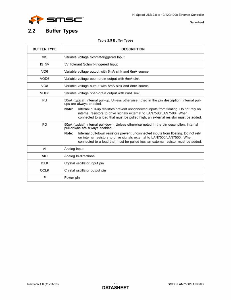
2.2 Buffer Types
Table 2.9 Buffer Types
BUFFER TYPE DESCRIPTION
VIS Variable voltage Schmitt-triggered Input
IS_5V 5V Tolerant Schmitt-triggered Input
VO6 Variable voltage output with 6mA sink and 6mA source
VOD6 Variable voltage open-drain output with 6mA sink
VO8 Variable voltage output with 8mA sink and 8mA source
VOD8 Variable voltage open-drain output with 8mA sink
PU 50uA (typical) internal pull-up. Unless otherwise noted in the pin description, internal pull-ups are always enabled.
Note: Internal pull-up resistors prevent unconnected inputs from floating. Do not rely on internal resistors to drive signals external to LAN7500/LAN7500i. When connected to a load that must be pulled high, an external resistor must be added.
PD 50uA (typical) internal pull-down. Unless otherwise noted in the pin description, internal pull-downs are always enabled.
Note: Internal pull-down resistors prevent unconnected inputs from floating. Do not rely on internal resistors to drive signals external to LAN7500/LAN7500i. When connected to a load that must be pulled low, an external resistor must be added.
AI Analog input
AIO Analog bi-directional
ICLK Crystal oscillator input pin
OCLK Crystal oscillator output pin
P Power pin
Revision 1.0 (11-01-10) 18 SMSC LAN7500/LAN7500iDATASHEET
Hi-Speed USB 2.0 to 10/100/1000 Ethernet Controller
Datasheet
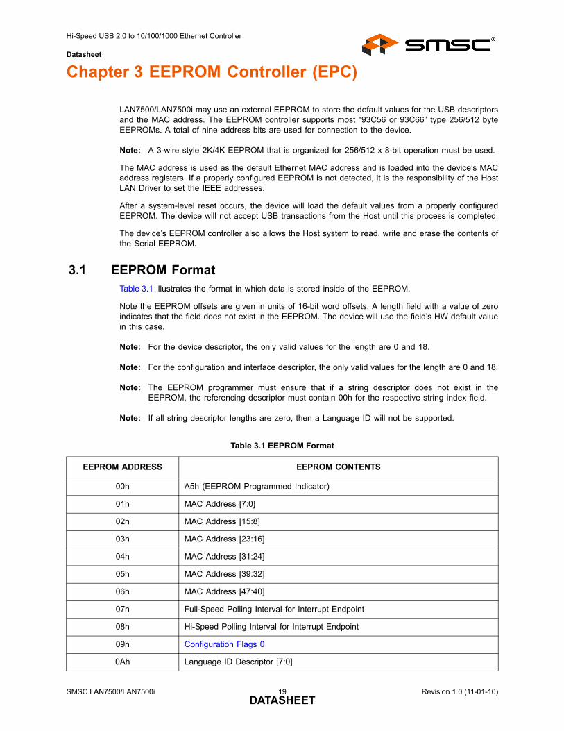
Chapter 3 EEPROM Controller (EPC)
LAN7500/LAN7500i may use an external EEPROM to store the default values for the USB descriptorsand the MAC address. The EEPROM controller supports most “93C56 or 93C66” type 256/512 byteEEPROMs. A total of nine address bits are used for connection to the device.
Note: A 3-wire style 2K/4K EEPROM that is organized for 256/512 x 8-bit operation must be used.
The MAC address is used as the default Ethernet MAC address and is loaded into the device’s MACaddress registers. If a properly configured EEPROM is not detected, it is the responsibility of the HostLAN Driver to set the IEEE addresses.
After a system-level reset occurs, the device will load the default values from a properly configuredEEPROM. The device will not accept USB transactions from the Host until this process is completed.
The device’s EEPROM controller also allows the Host system to read, write and erase the contents ofthe Serial EEPROM.
3.1 EEPROM FormatTable 3.1 illustrates the format in which data is stored inside of the EEPROM.
Note the EEPROM offsets are given in units of 16-bit word offsets. A length field with a value of zeroindicates that the field does not exist in the EEPROM. The device will use the field’s HW default valuein this case.
Note: For the device descriptor, the only valid values for the length are 0 and 18.
Note: For the configuration and interface descriptor, the only valid values for the length are 0 and 18.
Note: The EEPROM programmer must ensure that if a string descriptor does not exist in theEEPROM, the referencing descriptor must contain 00h for the respective string index field.
Note: If all string descriptor lengths are zero, then a Language ID will not be supported.
Table 3.1 EEPROM Format
EEPROM ADDRESS EEPROM CONTENTS
00h A5h (EEPROM Programmed Indicator)
01h MAC Address [7:0]
02h MAC Address [15:8]
03h MAC Address [23:16]
04h MAC Address [31:24]
05h MAC Address [39:32]
06h MAC Address [47:40]
07h Full-Speed Polling Interval for Interrupt Endpoint
08h Hi-Speed Polling Interval for Interrupt Endpoint
09h Configuration Flags 0
0Ah Language ID Descriptor [7:0]
SMSC LAN7500/LAN7500i 19 Revision 1.0 (11-01-10)DATASHEET

Hi-Speed USB 2.0 to 10/100/1000 Ethernet Controller
Datasheet
Note: EEPROM byte addresses past 21h can be used to store data for any purpose assuming theseaddresses are not used for descriptor storage.
0Bh Language ID Descriptor [15:8]
0Ch Manufacturer ID String Descriptor Length (bytes)
0Dh Manufacturer ID String Descriptor EEPROM Word Offset
0Eh Product Name String Descriptor Length (bytes)
0Fh Product Name String Descriptor EEPROM Word Offset
10h Serial Number String Descriptor Length (bytes)
11h Serial Number String Descriptor EEPROM Word Offset
12h Configuration String Descriptor Length (bytes)
13h Configuration String Descriptor Word Offset
14h Interface String Descriptor Length (bytes)
15h Interface String Descriptor Word Offset
16h Hi-Speed Device Descriptor Length (bytes)
17h Hi-Speed Device Descriptor Word Offset
18h Hi-Speed Configuration and Interface Descriptor Length (bytes)
19h Hi-Speed Configuration and Interface Descriptor Word Offset
1Ah Full-Speed Device Descriptor Length (bytes)
1Bh Full-Speed Device Descriptor Word Offset
1Ch Full-Speed Configuration and Interface Descriptor Length (bytes)
1Dh Full-Speed Configuration and Interface Descriptor Word Offset
1Eh GPIO[7:0] Wakeup EnablesBit x = 0 -> GPIOx Pin Disabled for Wakeup Use.Bit x = 1 -> GPIOx Pin Enabled for Wakeup Use.
1Fh GPI0[11:8] Wakeup EnablesBit x = 0 -> GPIO(x+8) Pin Disabled for Wakeup Use.Bit x = 1 -> GPIO(x+8) Pin Enabled for Wakeup Use.
Note: Bits 7:4 Unused.
20h GPIO PME Flags
21h Configuration Flags 1
Table 3.1 EEPROM Format (continued)
Revision 1.0 (11-01-10) 20 SMSC LAN7500/LAN7500iDATASHEET
Hi-Speed USB 2.0 to 10/100/1000 Ethernet Controller
Datasheet
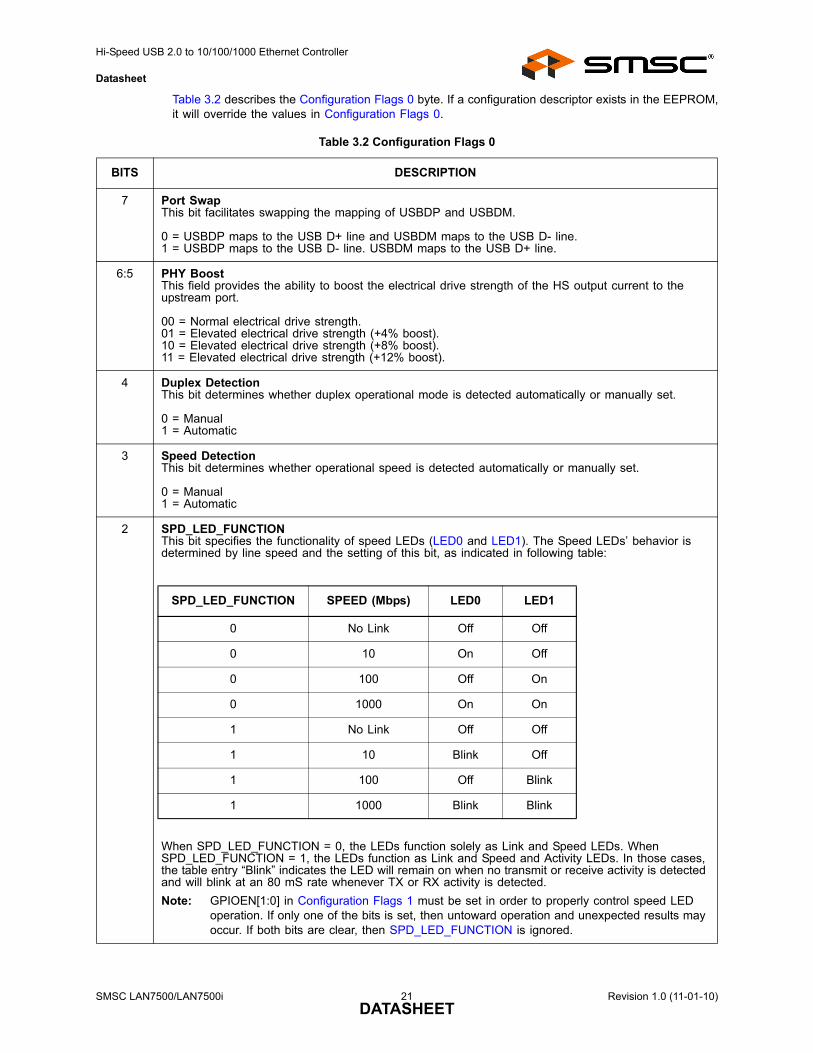
Table 3.2 describes the Configuration Flags 0 byte. If a configuration descriptor exists in the EEPROM,it will override the values in Configuration Flags 0.
Table 3.2 Configuration Flags 0
BITS DESCRIPTION
7 Port SwapThis bit facilitates swapping the mapping of USBDP and USBDM.
0 = USBDP maps to the USB D+ line and USBDM maps to the USB D- line.1 = USBDP maps to the USB D- line. USBDM maps to the USB D+ line.
6:5 PHY BoostThis field provides the ability to boost the electrical drive strength of the HS output current to the upstream port.
00 = Normal electrical drive strength.01 = Elevated electrical drive strength (+4% boost).10 = Elevated electrical drive strength (+8% boost).11 = Elevated electrical drive strength (+12% boost).
4 Duplex DetectionThis bit determines whether duplex operational mode is detected automatically or manually set.
0 = Manual1 = Automatic
3 Speed DetectionThis bit determines whether operational speed is detected automatically or manually set.
0 = Manual1 = Automatic
2 SPD_LED_FUNCTIONThis bit specifies the functionality of speed LEDs (LED0 and LED1). The Speed LEDs’ behavior is determined by line speed and the setting of this bit, as indicated in following table:
When SPD_LED_FUNCTION = 0, the LEDs function solely as Link and Speed LEDs. When SPD_LED_FUNCTION = 1, the LEDs function as Link and Speed and Activity LEDs. In those cases, the table entry “Blink” indicates the LED will remain on when no transmit or receive activity is detected and will blink at an 80 mS rate whenever TX or RX activity is detected.
Note: GPIOEN[1:0] in Configuration Flags 1 must be set in order to properly control speed LED operation. If only one of the bits is set, then untoward operation and unexpected results may occur. If both bits are clear, then SPD_LED_FUNCTION is ignored.
SPD_LED_FUNCTION SPEED (Mbps) LED0 LED1
0 No Link Off Off
0 10 On Off
0 100 Off On
0 1000 On On
1 No Link Off Off
1 10 Blink Off
1 100 Off Blink
1 1000 Blink Blink
SMSC LAN7500/LAN7500i 21 Revision 1.0 (11-01-10)DATASHEET
Hi-Speed USB 2.0 to 10/100/1000 Ethernet Controller
Datasheet
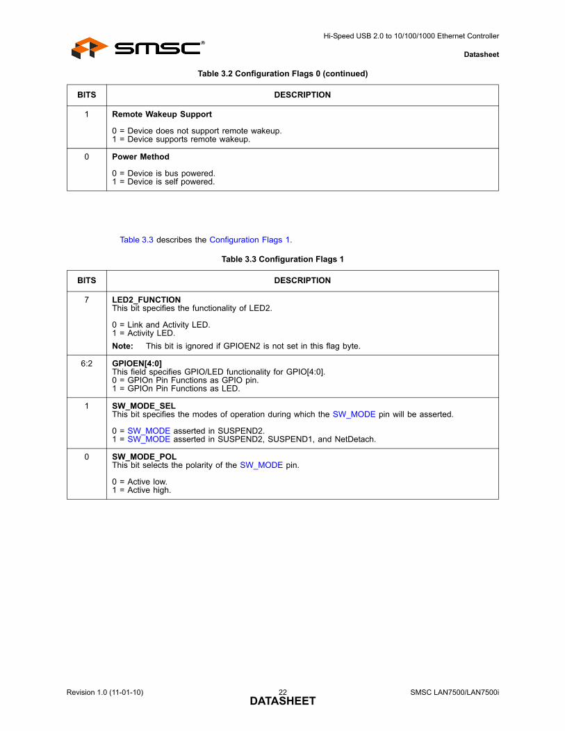
Table 3.3 describes the Configuration Flags 1.
1 Remote Wakeup Support
0 = Device does not support remote wakeup.1 = Device supports remote wakeup.
0 Power Method
0 = Device is bus powered.1 = Device is self powered.
Table 3.3 Configuration Flags 1
BITS DESCRIPTION
7 LED2_FUNCTIONThis bit specifies the functionality of LED2.
0 = Link and Activity LED.1 = Activity LED.
Note: This bit is ignored if GPIOEN2 is not set in this flag byte.
6:2 GPIOEN[4:0]This field specifies GPIO/LED functionality for GPIO[4:0]. 0 = GPIOn Pin Functions as GPIO pin.1 = GPIOn Pin Functions as LED.
1 SW_MODE_SELThis bit specifies the modes of operation during which the SW_MODE pin will be asserted.
0 = SW_MODE asserted in SUSPEND2.1 = SW_MODE asserted in SUSPEND2, SUSPEND1, and NetDetach.
0 SW_MODE_POLThis bit selects the polarity of the SW_MODE pin.
0 = Active low.1 = Active high.
Table 3.2 Configuration Flags 0 (continued)
BITS DESCRIPTION
Revision 1.0 (11-01-10) 22 SMSC LAN7500/LAN7500iDATASHEET
Hi-Speed USB 2.0 to 10/100/1000 Ethernet Controller
Datasheet
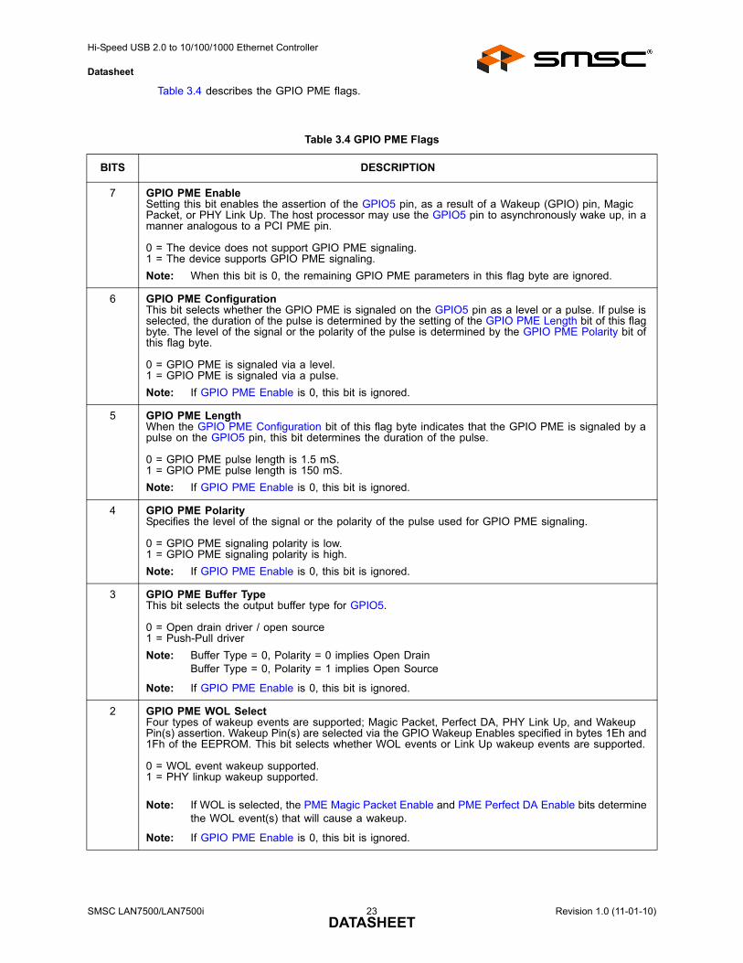
Table 3.4 describes the GPIO PME flags.
Table 3.4 GPIO PME Flags
BITS DESCRIPTION
7 GPIO PME EnableSetting this bit enables the assertion of the GPIO5 pin, as a result of a Wakeup (GPIO) pin, Magic Packet, or PHY Link Up. The host processor may use the GPIO5 pin to asynchronously wake up, in a manner analogous to a PCI PME pin.
0 = The device does not support GPIO PME signaling.1 = The device supports GPIO PME signaling.
Note: When this bit is 0, the remaining GPIO PME parameters in this flag byte are ignored.
6 GPIO PME ConfigurationThis bit selects whether the GPIO PME is signaled on the GPIO5 pin as a level or a pulse. If pulse is selected, the duration of the pulse is determined by the setting of the GPIO PME Length bit of this flag byte. The level of the signal or the polarity of the pulse is determined by the GPIO PME Polarity bit of this flag byte.
0 = GPIO PME is signaled via a level.1 = GPIO PME is signaled via a pulse.
Note: If GPIO PME Enable is 0, this bit is ignored.
5 GPIO PME LengthWhen the GPIO PME Configuration bit of this flag byte indicates that the GPIO PME is signaled by a pulse on the GPIO5 pin, this bit determines the duration of the pulse.
0 = GPIO PME pulse length is 1.5 mS.1 = GPIO PME pulse length is 150 mS.
Note: If GPIO PME Enable is 0, this bit is ignored.
4 GPIO PME PolaritySpecifies the level of the signal or the polarity of the pulse used for GPIO PME signaling.
0 = GPIO PME signaling polarity is low.1 = GPIO PME signaling polarity is high.
Note: If GPIO PME Enable is 0, this bit is ignored.
3 GPIO PME Buffer TypeThis bit selects the output buffer type for GPIO5.
0 = Open drain driver / open source1 = Push-Pull driver
Note: Buffer Type = 0, Polarity = 0 implies Open DrainBuffer Type = 0, Polarity = 1 implies Open Source
Note: If GPIO PME Enable is 0, this bit is ignored.
2 GPIO PME WOL SelectFour types of wakeup events are supported; Magic Packet, Perfect DA, PHY Link Up, and Wakeup Pin(s) assertion. Wakeup Pin(s) are selected via the GPIO Wakeup Enables specified in bytes 1Eh and 1Fh of the EEPROM. This bit selects whether WOL events or Link Up wakeup events are supported.
0 = WOL event wakeup supported.1 = PHY linkup wakeup supported.
Note: If WOL is selected, the PME Magic Packet Enable and PME Perfect DA Enable bits determine the WOL event(s) that will cause a wakeup.
Note: If GPIO PME Enable is 0, this bit is ignored.
SMSC LAN7500/LAN7500i 23 Revision 1.0 (11-01-10)DATASHEET
Hi-Speed USB 2.0 to 10/100/1000 Ethernet Controller
Datasheet
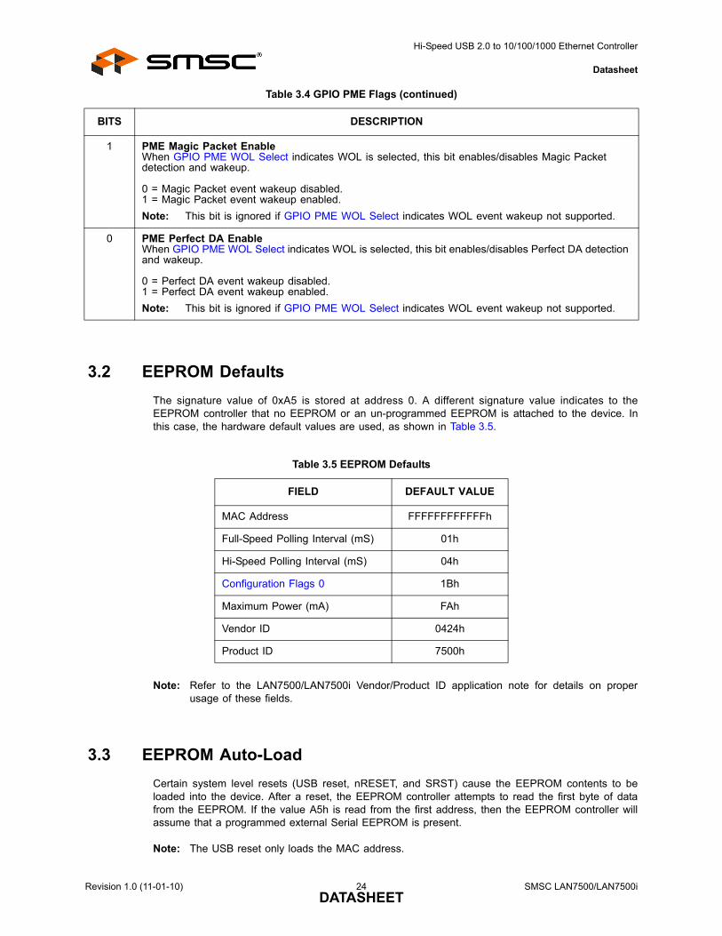
3.2 EEPROM Defaults
The signature value of 0xA5 is stored at address 0. A different signature value indicates to theEEPROM controller that no EEPROM or an un-programmed EEPROM is attached to the device. Inthis case, the hardware default values are used, as shown in Table 3.5.
Note: Refer to the LAN7500/LAN7500i Vendor/Product ID application note for details on properusage of these fields.
3.3 EEPROM Auto-Load
Certain system level resets (USB reset, nRESET, and SRST) cause the EEPROM contents to beloaded into the device. After a reset, the EEPROM controller attempts to read the first byte of datafrom the EEPROM. If the value A5h is read from the first address, then the EEPROM controller willassume that a programmed external Serial EEPROM is present.
Note: The USB reset only loads the MAC address.
1 PME Magic Packet EnableWhen GPIO PME WOL Select indicates WOL is selected, this bit enables/disables Magic Packet detection and wakeup.
0 = Magic Packet event wakeup disabled.1 = Magic Packet event wakeup enabled.
Note: This bit is ignored if GPIO PME WOL Select indicates WOL event wakeup not supported.
0 PME Perfect DA EnableWhen GPIO PME WOL Select indicates WOL is selected, this bit enables/disables Perfect DA detection and wakeup.
0 = Perfect DA event wakeup disabled.1 = Perfect DA event wakeup enabled.
Note: This bit is ignored if GPIO PME WOL Select indicates WOL event wakeup not supported.
Table 3.5 EEPROM Defaults
FIELD DEFAULT VALUE
MAC Address FFFFFFFFFFFFh
Full-Speed Polling Interval (mS) 01h
Hi-Speed Polling Interval (mS) 04h
Configuration Flags 0 1Bh
Maximum Power (mA) FAh
Vendor ID 0424h
Product ID 7500h
Table 3.4 GPIO PME Flags (continued)
BITS DESCRIPTION
Revision 1.0 (11-01-10) 24 SMSC LAN7500/LAN7500iDATASHEET
Hi-Speed USB 2.0 to 10/100/1000 Ethernet Controller
Datasheet
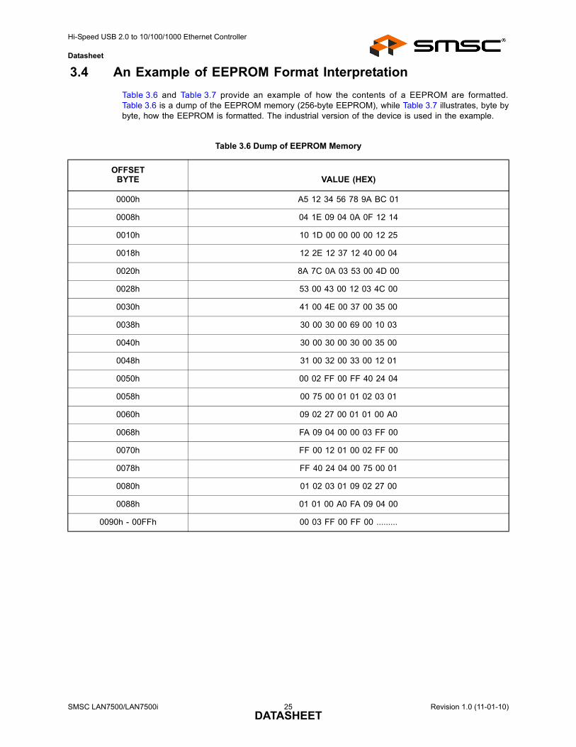
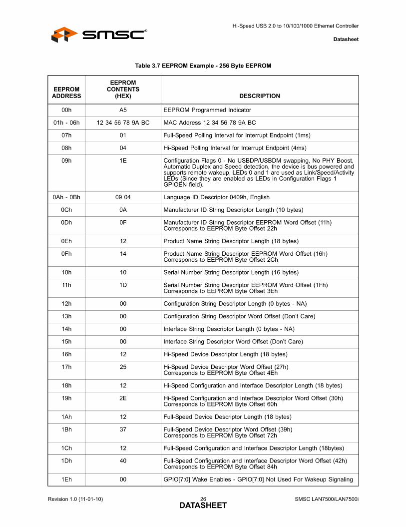
3.4 An Example of EEPROM Format Interpretation
Table 3.6 and Table 3.7 provide an example of how the contents of a EEPROM are formatted.Table 3.6 is a dump of the EEPROM memory (256-byte EEPROM), while Table 3.7 illustrates, byte bybyte, how the EEPROM is formatted. The industrial version of the device is used in the example.
Table 3.6 Dump of EEPROM Memory
OFFSETBYTE VALUE (HEX)
0000h A5 12 34 56 78 9A BC 01
0008h 04 1E 09 04 0A 0F 12 14
0010h 10 1D 00 00 00 00 12 25
0018h 12 2E 12 37 12 40 00 04
0020h 8A 7C 0A 03 53 00 4D 00
0028h 53 00 43 00 12 03 4C 00
0030h 41 00 4E 00 37 00 35 00
0038h 30 00 30 00 69 00 10 03
0040h 30 00 30 00 30 00 35 00
0048h 31 00 32 00 33 00 12 01
0050h 00 02 FF 00 FF 40 24 04
0058h 00 75 00 01 01 02 03 01
0060h 09 02 27 00 01 01 00 A0
0068h FA 09 04 00 00 03 FF 00
0070h FF 00 12 01 00 02 FF 00
0078h FF 40 24 04 00 75 00 01
0080h 01 02 03 01 09 02 27 00
0088h 01 01 00 A0 FA 09 04 00
0090h - 00FFh 00 03 FF 00 FF 00 .........
SMSC LAN7500/LAN7500i 25 Revision 1.0 (11-01-10)DATASHEET
Hi-Speed USB 2.0 to 10/100/1000 Ethernet Controller
Datasheet
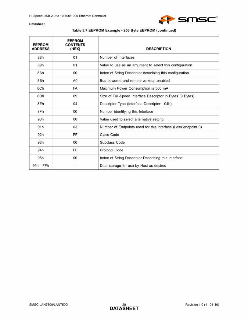
Table 3.7 EEPROM Example - 256 Byte EEPROM
EEPROMADDRESS
EEPROMCONTENTS
(HEX) DESCRIPTION
00h A5 EEPROM Programmed Indicator
01h - 06h 12 34 56 78 9A BC MAC Address 12 34 56 78 9A BC
07h 01 Full-Speed Polling Interval for Interrupt Endpoint (1ms)
08h 04 Hi-Speed Polling Interval for Interrupt Endpoint (4ms)
09h 1E Configuration Flags 0 - No USBDP/USBDM swapping, No PHY Boost, Automatic Duplex and Speed detection, the device is bus powered and supports remote wakeup, LEDs 0 and 1 are used as Link/Speed/Activity LEDs (Since they are enabled as LEDs in Configuration Flags 1 GPIOEN field).
0Ah - 0Bh 09 04 Language ID Descriptor 0409h, English
0Ch 0A Manufacturer ID String Descriptor Length (10 bytes)
0Dh 0F Manufacturer ID String Descriptor EEPROM Word Offset (11h)Corresponds to EEPROM Byte Offset 22h
0Eh 12 Product Name String Descriptor Length (18 bytes)
0Fh 14 Product Name String Descriptor EEPROM Word Offset (16h)Corresponds to EEPROM Byte Offset 2Ch
10h 10 Serial Number String Descriptor Length (16 bytes)
11h 1D Serial Number String Descriptor EEPROM Word Offset (1Fh)Corresponds to EEPROM Byte Offset 3Eh
12h 00 Configuration String Descriptor Length (0 bytes - NA)
13h 00 Configuration String Descriptor Word Offset (Don’t Care)
14h 00 Interface String Descriptor Length (0 bytes - NA)
15h 00 Interface String Descriptor Word Offset (Don’t Care)
16h 12 Hi-Speed Device Descriptor Length (18 bytes)
17h 25 Hi-Speed Device Descriptor Word Offset (27h)Corresponds to EEPROM Byte Offset 4Eh
18h 12 Hi-Speed Configuration and Interface Descriptor Length (18 bytes)
19h 2E Hi-Speed Configuration and Interface Descriptor Word Offset (30h)Corresponds to EEPROM Byte Offset 60h
1Ah 12 Full-Speed Device Descriptor Length (18 bytes)
1Bh 37 Full-Speed Device Descriptor Word Offset (39h)Corresponds to EEPROM Byte Offset 72h
1Ch 12 Full-Speed Configuration and Interface Descriptor Length (18bytes)
1Dh 40 Full-Speed Configuration and Interface Descriptor Word Offset (42h)Corresponds to EEPROM Byte Offset 84h
1Eh 00 GPIO[7:0] Wake Enables - GPIO[7:0] Not Used For Wakeup Signaling
Revision 1.0 (11-01-10) 26 SMSC LAN7500/LAN7500iDATASHEET
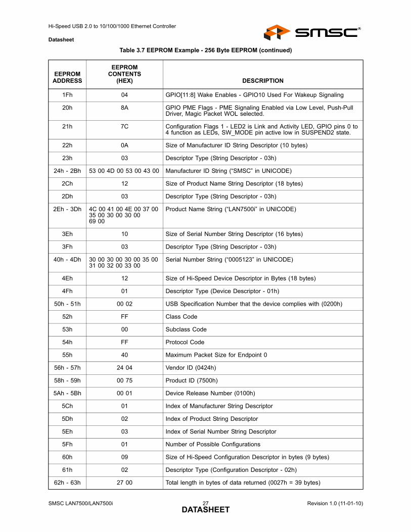
Hi-Speed USB 2.0 to 10/100/1000 Ethernet Controller
Datasheet
1Fh 04 GPIO[11:8] Wake Enables - GPIO10 Used For Wakeup Signaling
20h 8A GPIO PME Flags - PME Signaling Enabled via Low Level, Push-Pull Driver, Magic Packet WOL selected.
21h 7C Configuration Flags 1 - LED2 is Link and Activity LED, GPIO pins 0 to 4 function as LEDs, SW_MODE pin active low in SUSPEND2 state.
22h 0A Size of Manufacturer ID String Descriptor (10 bytes)
23h 03 Descriptor Type (String Descriptor - 03h)
24h - 2Bh 53 00 4D 00 53 00 43 00 Manufacturer ID String (“SMSC” in UNICODE)
2Ch 12 Size of Product Name String Descriptor (18 bytes)
2Dh 03 Descriptor Type (String Descriptor - 03h)
2Eh - 3Dh 4C 00 41 00 4E 00 37 00 35 00 30 00 30 0069 00
Product Name String (“LAN7500i” in UNICODE)
3Eh 10 Size of Serial Number String Descriptor (16 bytes)
3Fh 03 Descriptor Type (String Descriptor - 03h)
40h - 4Dh 30 00 30 00 30 00 35 00 31 00 32 00 33 00
Serial Number String (“0005123” in UNICODE)
4Eh 12 Size of Hi-Speed Device Descriptor in Bytes (18 bytes)
4Fh 01 Descriptor Type (Device Descriptor - 01h)
50h - 51h 00 02 USB Specification Number that the device complies with (0200h)
52h FF Class Code
53h 00 Subclass Code
54h FF Protocol Code
55h 40 Maximum Packet Size for Endpoint 0
56h - 57h 24 04 Vendor ID (0424h)
58h - 59h 00 75 Product ID (7500h)
5Ah - 5Bh 00 01 Device Release Number (0100h)
5Ch 01 Index of Manufacturer String Descriptor
5Dh 02 Index of Product String Descriptor
5Eh 03 Index of Serial Number String Descriptor
5Fh 01 Number of Possible Configurations
60h 09 Size of Hi-Speed Configuration Descriptor in bytes (9 bytes)
61h 02 Descriptor Type (Configuration Descriptor - 02h)
62h - 63h 27 00 Total length in bytes of data returned (0027h = 39 bytes)
Table 3.7 EEPROM Example - 256 Byte EEPROM (continued)
EEPROMADDRESS
EEPROMCONTENTS
(HEX) DESCRIPTION
SMSC LAN7500/LAN7500i 27 Revision 1.0 (11-01-10)DATASHEET
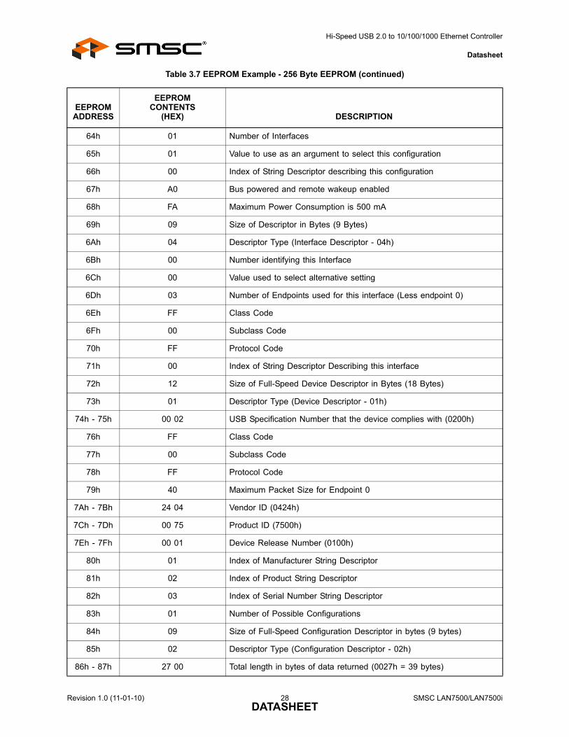
Hi-Speed USB 2.0 to 10/100/1000 Ethernet Controller
Datasheet
64h 01 Number of Interfaces
65h 01 Value to use as an argument to select this configuration
66h 00 Index of String Descriptor describing this configuration
67h A0 Bus powered and remote wakeup enabled
68h FA Maximum Power Consumption is 500 mA
69h 09 Size of Descriptor in Bytes (9 Bytes)
6Ah 04 Descriptor Type (Interface Descriptor - 04h)
6Bh 00 Number identifying this Interface
6Ch 00 Value used to select alternative setting
6Dh 03 Number of Endpoints used for this interface (Less endpoint 0)
6Eh FF Class Code
6Fh 00 Subclass Code
70h FF Protocol Code
71h 00 Index of String Descriptor Describing this interface
72h 12 Size of Full-Speed Device Descriptor in Bytes (18 Bytes)
73h 01 Descriptor Type (Device Descriptor - 01h)
74h - 75h 00 02 USB Specification Number that the device complies with (0200h)
76h FF Class Code
77h 00 Subclass Code
78h FF Protocol Code
79h 40 Maximum Packet Size for Endpoint 0
7Ah - 7Bh 24 04 Vendor ID (0424h)
7Ch - 7Dh 00 75 Product ID (7500h)
7Eh - 7Fh 00 01 Device Release Number (0100h)
80h 01 Index of Manufacturer String Descriptor
81h 02 Index of Product String Descriptor
82h 03 Index of Serial Number String Descriptor
83h 01 Number of Possible Configurations
84h 09 Size of Full-Speed Configuration Descriptor in bytes (9 bytes)
85h 02 Descriptor Type (Configuration Descriptor - 02h)
86h - 87h 27 00 Total length in bytes of data returned (0027h = 39 bytes)
Table 3.7 EEPROM Example - 256 Byte EEPROM (continued)
EEPROMADDRESS
EEPROMCONTENTS
(HEX) DESCRIPTION
Revision 1.0 (11-01-10) 28 SMSC LAN7500/LAN7500iDATASHEET
Hi-Speed USB 2.0 to 10/100/1000 Ethernet Controller
Datasheet
88h 01 Number of Interfaces
89h 01 Value to use as an argument to select this configuration
8Ah 00 Index of String Descriptor describing this configuration
8Bh A0 Bus powered and remote wakeup enabled
8Ch FA Maximum Power Consumption is 500 mA
8Dh 09 Size of Full-Speed Interface Descriptor in Bytes (9 Bytes)
8Eh 04 Descriptor Type (Interface Descriptor - 04h)
8Fh 00 Number identifying this Interface
90h 00 Value used to select alternative setting
91h 03 Number of Endpoints used for this interface (Less endpoint 0)
92h FF Class Code
93h 00 Subclass Code
94h FF Protocol Code
95h 00 Index of String Descriptor Describing this interface
96h - FFh - Data storage for use by Host as desired
Table 3.7 EEPROM Example - 256 Byte EEPROM (continued)
EEPROMADDRESS
EEPROMCONTENTS
(HEX) DESCRIPTION
SMSC LAN7500/LAN7500i 29 Revision 1.0 (11-01-10)DATASHEET

Hi-Speed USB 2.0 to 10/100/1000 Ethernet Controller
Datasheet
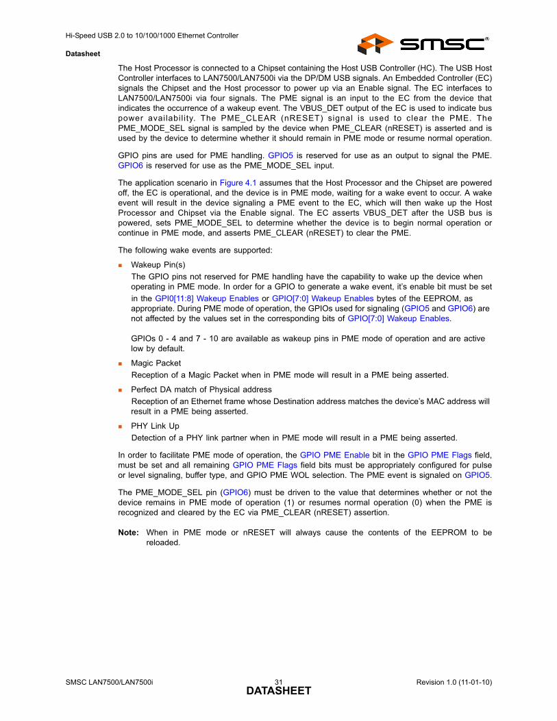
Chapter 4 PME Operation
LAN7500/LAN7500i provides a mechanism for waking up a host system via PME mode of operation.PME signaling is only available while the device is operating in the self powered mode and a properlyconfigured EEPROM is attached. Figure 4.1 illustrates a typical application.
Figure 4.1 Typical Application
LAN7500/LAN7500i
Embedded Controller
(EC)
Chipset
DP/DM
PME
PME_MODE_SEL
Enable
HC
PME_CLEAR
VBUS_DET
EEPROM
HostProcessor
Revision 1.0 (11-01-10) 30 SMSC LAN7500/LAN7500iDATASHEET
Hi-Speed USB 2.0 to 10/100/1000 Ethernet Controller
Datasheet
The Host Processor is connected to a Chipset containing the Host USB Controller (HC). The USB HostController interfaces to LAN7500/LAN7500i via the DP/DM USB signals. An Embedded Controller (EC)signals the Chipset and the Host processor to power up via an Enable signal. The EC interfaces toLAN7500/LAN7500i via four signals. The PME signal is an input to the EC from the device thatindicates the occurrence of a wakeup event. The VBUS_DET output of the EC is used to indicate buspower availabil ity. The PME_CLEAR (nRESET) signal is used to clear the PME. ThePME_MODE_SEL signal is sampled by the device when PME_CLEAR (nRESET) is asserted and isused by the device to determine whether it should remain in PME mode or resume normal operation.
GPIO pins are used for PME handling. GPIO5 is reserved for use as an output to signal the PME.GPIO6 is reserved for use as the PME_MODE_SEL input.
The application scenario in Figure 4.1 assumes that the Host Processor and the Chipset are poweredoff, the EC is operational, and the device is in PME mode, waiting for a wake event to occur. A wakeevent will result in the device signaling a PME event to the EC, which will then wake up the HostProcessor and Chipset via the Enable signal. The EC asserts VBUS_DET after the USB bus ispowered, sets PME_MODE_SEL to determine whether the device is to begin normal operation orcontinue in PME mode, and asserts PME_CLEAR (nRESET) to clear the PME.
The following wake events are supported:
Wakeup Pin(s)
The GPIO pins not reserved for PME handling have the capability to wake up the device when operating in PME mode. In order for a GPIO to generate a wake event, it’s enable bit must be set
in the GPI0[11:8] Wakeup Enables or GPIO[7:0] Wakeup Enables bytes of the EEPROM, as appropriate. During PME mode of operation, the GPIOs used for signaling (GPIO5 and GPIO6) are not affected by the values set in the corresponding bits of GPIO[7:0] Wakeup Enables.
GPIOs 0 - 4 and 7 - 10 are available as wakeup pins in PME mode of operation and are active low by default.
Magic Packet
Reception of a Magic Packet when in PME mode will result in a PME being asserted.
Perfect DA match of Physical address
Reception of an Ethernet frame whose Destination address matches the device’s MAC address will result in a PME being asserted.
PHY Link Up
Detection of a PHY link partner when in PME mode will result in a PME being asserted.
In order to facilitate PME mode of operation, the GPIO PME Enable bit in the GPIO PME Flags field,must be set and all remaining GPIO PME Flags field bits must be appropriately configured for pulseor level signaling, buffer type, and GPIO PME WOL selection. The PME event is signaled on GPIO5.
The PME_MODE_SEL pin (GPIO6) must be driven to the value that determines whether or not thedevice remains in PME mode of operation (1) or resumes normal operation (0) when the PME isrecognized and cleared by the EC via PME_CLEAR (nRESET) assertion.
Note: When in PME mode or nRESET will always cause the contents of the EEPROM to bereloaded.
SMSC LAN7500/LAN7500i 31 Revision 1.0 (11-01-10)DATASHEET

Hi-Speed USB 2.0 to 10/100/1000 Ethernet Controller
Datasheet
Figure 4.2 flowcharts PME operation while in Internal PHY mode. The following conditions hold:
EEPROM Configuration:
GPIO PME Enable = 1 (enabled)
GPIO PME Configuration = 0 (PME signaled via level on GPIO5 pin)
GPIO PME Length = 0 (NA)
GPIO PME Polarity = 1 (high level signals event)
GPIO PME Buffer Type = 1 (Push-Pull)
GPIO PME WOL Select = 0 (Magic Packet wakeup)
Power Method = 1 (self powered)
MAC address for Magic Packet
PME signaling configuration:
GPIO5 signals PME
GPIO6 is PME_MODE_SEL
Revision 1.0 (11-01-10) 32 SMSC LAN7500/LAN7500iDATASHEET

Hi-Speed USB 2.0 to 10/100/1000 Ethernet Controller
Datasheet
Figure 4.2 PME Operation
Wakeup Event Detected By LAN7500/LAN7500i?
LAN7500/LAN7500i Asserts PME
True
False
Deassert PME_CEAR
LAN7500/LAN7500i Has EEPROM With GPIO PME Enable =1, Enters
PME Mode
EC Detects PME
EC To Wake System To Process Wakeup Event?
EC Asserts PME_CLEAR
LAN7500/LAN7500i Resets And Deasserts PME
VBUS_DET Set to 1 By EC Or Via Circuitry
EC Sets PME_MODE_SEL = 0 And Asserts PME_CLEAR
EC Signals Enable To Host
LAN7500/LAN7500i Resets And Deasserts PME
LAN7500/LAN7500i Connects To USB Bus
LAN7500/LAN7500i Is In Normal Operation
Yes
No
Host & Chipset Powered Off
VBUS_DET Set To 0 By ECOr Via Circuitry
EC Sets PME_MODE_SEL = 1 And Asserts PME_CLEAR
SMSC LAN7500/LAN7500i 33 Revision 1.0 (11-01-10)DATASHEET
Hi-Speed USB 2.0 to 10/100/1000 Ethernet Controller
Datasheet
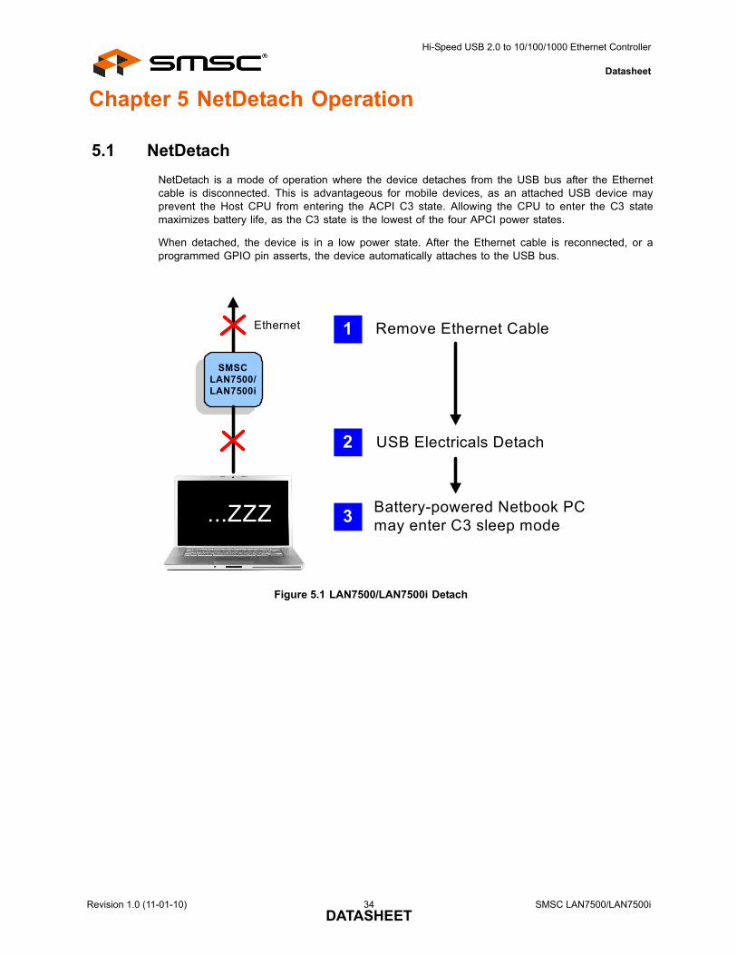
Chapter 5 NetDetach Operation
5.1 NetDetach
NetDetach is a mode of operation where the device detaches from the USB bus after the Ethernetcable is disconnected. This is advantageous for mobile devices, as an attached USB device mayprevent the Host CPU from entering the ACPI C3 state. Allowing the CPU to enter the C3 statemaximizes battery life, as the C3 state is the lowest of the four APCI power states.
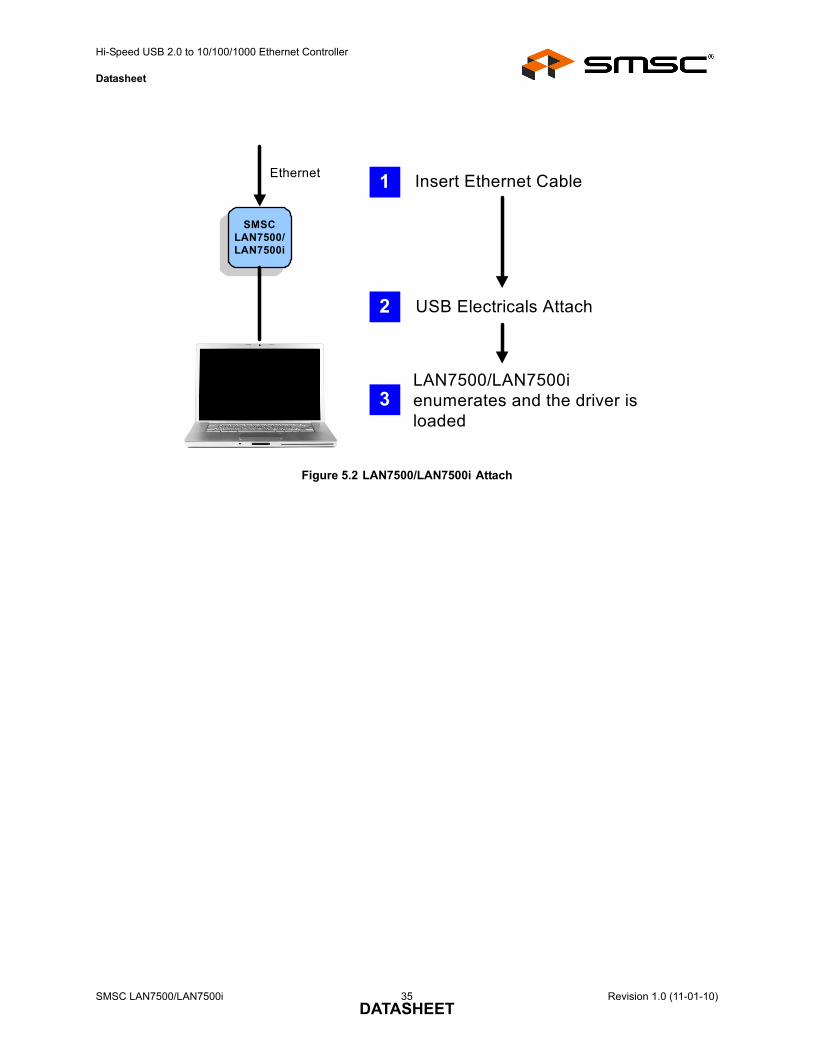
When detached, the device is in a low power state. After the Ethernet cable is reconnected, or aprogrammed GPIO pin asserts, the device automatically attaches to the USB bus.
Figure 5.1 LAN7500/LAN7500i Detach
USB Electricals Detach
Remove Ethernet Cable1
...ZZZ
2
Battery-powered Netbook PC may enter C3 sleep mode3
Ethernet
SMSC LAN7500/LAN7500i
Revision 1.0 (11-01-10) 34 SMSC LAN7500/LAN7500iDATASHEET
Hi-Speed USB 2.0 to 10/100/1000 Ethernet Controller
Datasheet
Figure 5.2 LAN7500/LAN7500i Attach
USB Electricals Attach
Insert Ethernet Cable1
2
LAN7500/LAN7500i enumerates and the driver is loaded
3
Ethernet
SMSC LAN7500/ LAN7500i
SMSC LAN7500/LAN7500i 35 Revision 1.0 (11-01-10)DATASHEET
Hi-Speed USB 2.0 to 10/100/1000 Ethernet Controller
Datasheet
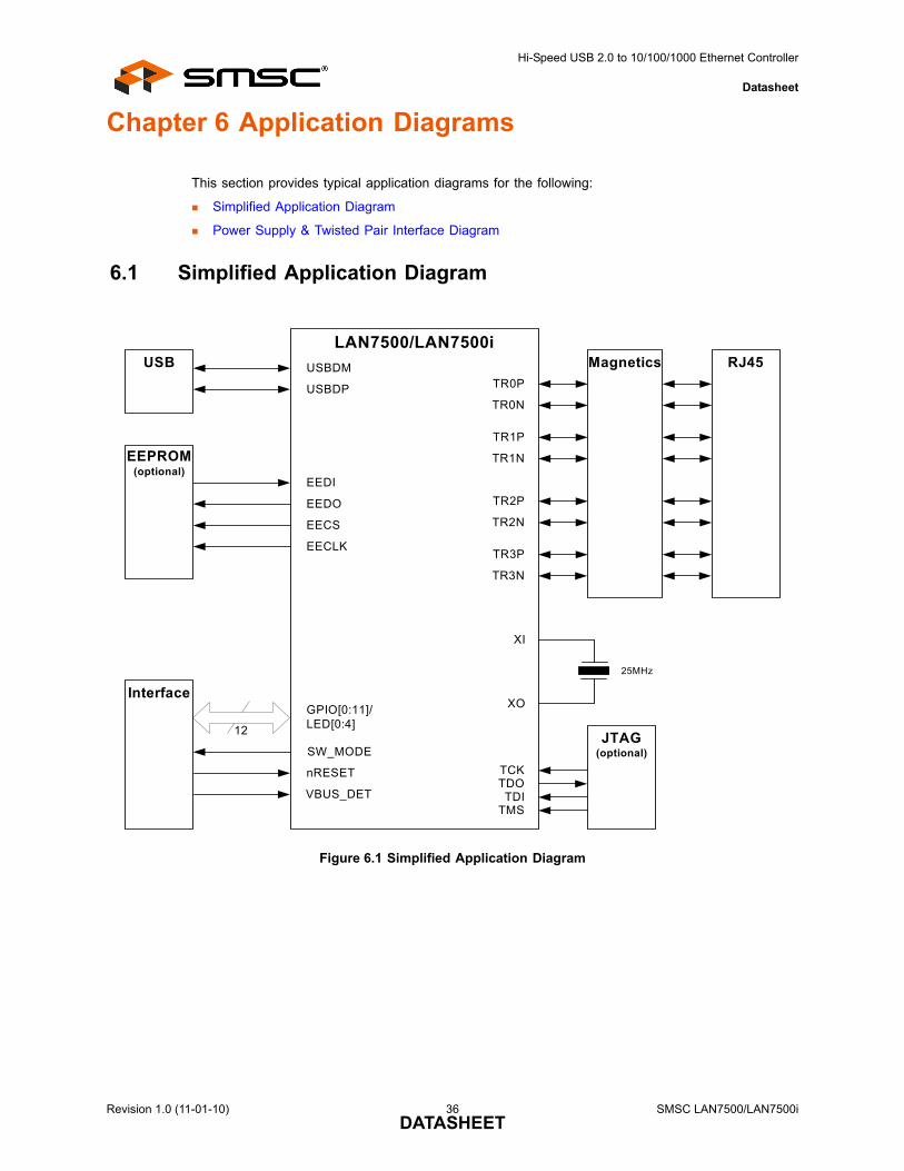
Chapter 6 Application Diagrams
This section provides typical application diagrams for the following:
Simplified Application Diagram
Power Supply & Twisted Pair Interface Diagram
6.1 Simplified Application Diagram
Figure 6.1 Simplified Application Diagram
LAN7500/LAN7500i
TR0P
TR0N
Magnetics RJ45
TR1P
TR1N
TR2P
TR2N
TR3P
TR3N
25MHz
GPIO[0:11]/LED[0:4]12
Interface
USBDM
USBDP
nRESET
VBUS_DET
XI
XO
JTAG(optional)
TDITMS
TCKTDO
USB
SW_MODE
EEPROM (optional)
EEDI
EEDO
EECS
EECLK
Revision 1.0 (11-01-10) 36 SMSC LAN7500/LAN7500iDATASHEET
Hi-Speed USB 2.0 to 10/100/1000 Ethernet Controller
Datasheet
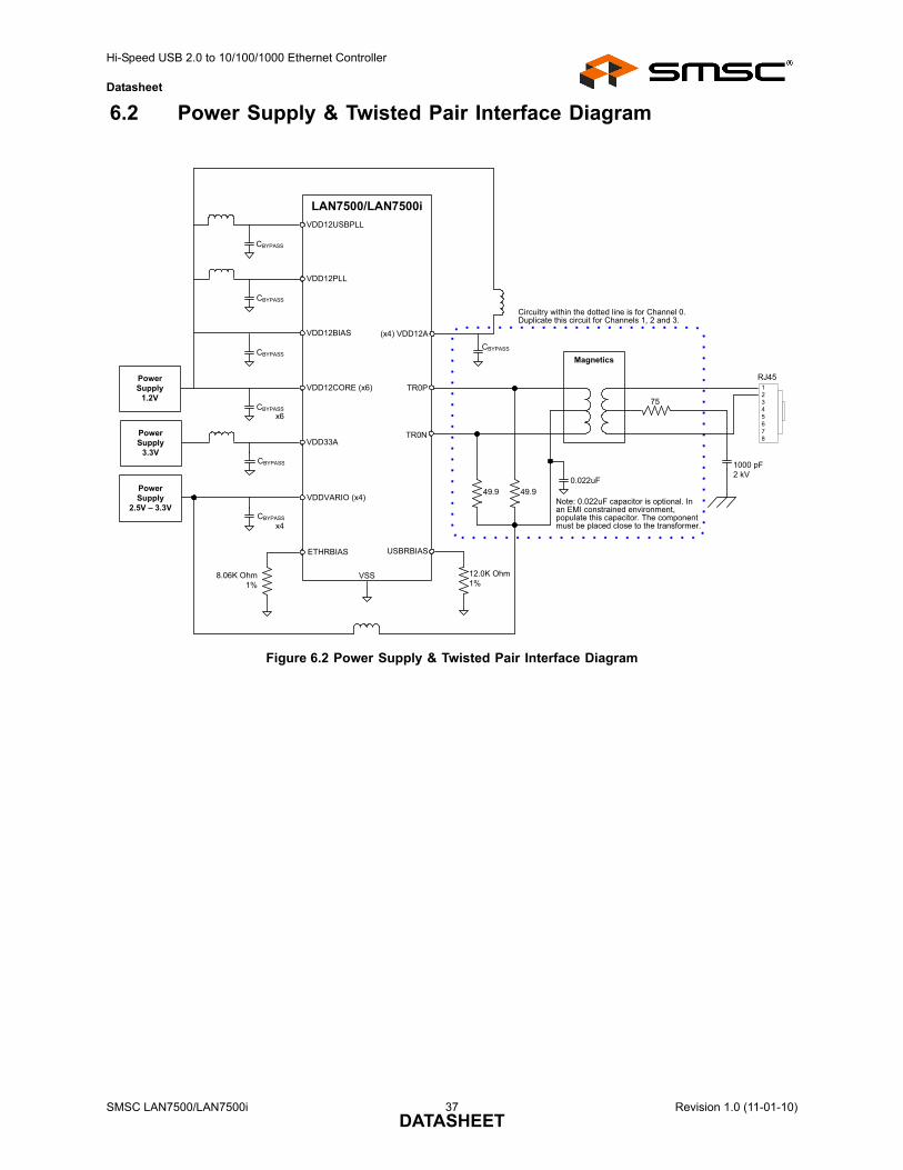
6.2 Power Supply & Twisted Pair Interface Diagram
Figure 6.2 Power Supply & Twisted Pair Interface Diagram
LAN7500/LAN7500i
VSS
VDD12PLL
CBYPASS
VDD12BIAS
CBYPASS
VDD12CORE (x6)
CBYPASS
VDDVARIO (x4)
CBYPASS
x6
x4
PowerSupply
2.5V – 3.3V
PowerSupply
1.2V
VDD12USBPLL
(x4) VDD12A
USBRBIAS
12.0K Ohm 1%
CBYPASS
VDD33APowerSupply
3.3VCBYPASS
ETHRBIAS
8.06K Ohm 1%
Magnetics
TR0P
TR0N
12345678
1000 pF2 kV
Circuitry within the dotted line is for Channel 0.Duplicate this circuit for Channels 1, 2 and 3.
RJ45
75
CBYPASS
49.9 49.90.022uF
Note: 0.022uF capacitor is optional. In an EMI constrained environment, populate this capacitor. The component must be placed close to the transformer.
SMSC LAN7500/LAN7500i 37 Revision 1.0 (11-01-10)DATASHEET
Hi-Speed USB 2.0 to 10/100/1000 Ethernet Controller
Datasheet
Chapter 7 Operational Characteristics
7.1 Absolute Maximum Ratings*
Supply Voltage (VDDVARIO) (Note 7.1). . . . . . . . . . . . . . . . . . . . . . . . . . . . . . . . . . . . . . -0.5V to +3.6V
Analog Supply Voltage (VDD12A) (Note 7.1) . . . . . . . . . . . . . . . . . . . . . . . . . . . . . . . . . . -0.5V to +1.5V
Analog USB Supply Voltage (VDD33A) (Note 7.1) . . . . . . . . . . . . . . . . . . . . . . . . . . . . . -0.5V to +3.6V
Digital Core Supply Voltage (VDD12CORE) (Note 7.1) . . . . . . . . . . . . . . . . . . . . . . . . . . -0.5V to +1.5V
Ethernet Magnetics Supply Voltage . . . . . . . . . . . . . . . . . . . . . . . . . . . . . . . . . . . . . . . . . -0.5V to +3.6V
Positive voltage on signal pins, with respect to ground (Note 7.2) . . . . . . . . . . . . . . . . . . . . . . . . +6.0V
Negative voltage on signal pins, with respect to ground (Note 7.3) . . . . . . . . . . . . . . . . . . . . . . . . -0.5V
Positive voltage on XI, with respect to ground. . . . . . . . . . . . . . . . . . . . . . . . . . . . . . . . . . . . . . . . +4.6V
Positive voltage on XO, with respect to ground. . . . . . . . . . . . . . . . . . . . . . . . . . . . . . . . . . . . . . . +2.5V
Ambient Operating Temperature in Still Air (TA). . . . . . . . . . . . . . . . . . . . . . . . . . . . . . . . . . . . . Note 7.4
Junction to Ambient (θJA) . . . . . . . . . . . . . . . . . . . . . . . . . . . . . . . . . . . . . . . . . . . . . . . . . . . . . .24.4oC/W
Junction to Top of Package (ΨJT) . . . . . . . . . . . . . . . . . . . . . . . . . . . . . . . . . . . . . . . . . . . . . . . .0.1oC/W
Storage Temperature. . . . . . . . . . . . . . . . . . . . . . . . . . . . . . . . . . . . . . . . . . . . . . . . . . . .-55oC to +150oC
Lead Temperature Range . . . . . . . . . . . . . . . . . . . . . . . . . . . . . . . . . Refer to JEDEC Spec. J-STD-020
HBM ESD Performance . . . . . . . . . . . . . . . . . . . . . . . . . . . . . . . . . . . . . . . . . . . . . . . . .JEDEC Class 3A
Latch-up Performance per EIA/JESD 78 . . . . . . . . . . . . . . . . . . . . . . . . . . . . . . . . . . . . . . . . . .+/-150mA
Note 7.1 When powering this device from laboratory or system power supplies, it is important thatthe absolute maximum ratings not be exceeded or device failure can result. Some powersupplies exhibit voltage spikes on their outputs when AC power is switched on or off. Inaddition, voltage transients on the AC power line may appear on the DC output. If thispossibility exists, it is suggested that a clamp circuit be used.
Note 7.2 This rating does not apply to the following pins: XI, XO, ETHRBIAS, USBRBIAS.
Note 7.3 This rating does not apply to the following pins: ETHRBIAS, USBRBIAS.
Note 7.4 0oC to +70oC for commercial version, -40oC to +85oC for industrial version.
*Stresses exceeding those listed in this section could cause permanent damage to the device. This isa stress rating only. Exposure to absolute maximum rating conditions for extended periods may affectdevice reliability. Functional operation of the device at any condition exceeding those indicated inSection 7.2, "Operating Conditions**", Section 7.4, "DC Specifications", or any other applicable sectionof this specification is not implied. Note, device signals are NOT 5 volt tolerant unless specifiedotherwise.
Revision 1.0 (11-01-10) 38 SMSC LAN7500/LAN7500iDATASHEET
Hi-Speed USB 2.0 to 10/100/1000 Ethernet Controller
Datasheet
7.2 Operating Conditions**
Supply Voltage (VDDVARIO) . . . . . . . . . . . . . . . . . . . . . . . . . . . . . . . . . . . . . . . . . . . . . +2.25V to +3.6V
Supply Voltage (VDD12A). . . . . . . . . . . . . . . . . . . . . . . . . . . . . . . . . . . . . . . . . . . . . . . +1.14V to +1.26V
Analog USB Supply Voltage (VDD33A) . . . . . . . . . . . . . . . . . . . . . . . . . . . . . . . . . . . . . +3.0V to +3.6V
Digital Core Supply Voltage (VDD12CORE) . . . . . . . . . . . . . . . . . . . . . . . . . . . . . . . . +1.14V to +1.26V
Ethernet Magnetics Supply Voltage . . . . . . . . . . . . . . . . . . . . . . . . . . . . . . . . . . . . . . . . +2.25V to +3.6V
Ambient Operating Temperature in Still Air (TA). . . . . . . . . . . . . . . . . . . . . . . . . . . . . . . . . . . . . Note 7.4
**Proper operation of the device is guaranteed only within the ranges specified in this section. Afterthe device has completed power-up, VDDVARIO and the magnetics power supply must maintain theirvoltage level with +/-10%. Varying the voltage greater than +/-10% after the device has completedpower-up can cause errors in device operation.
7.3 Power Consumption
This section details the power consumption of the device as measured during various modes ofoperation. For each mode of operation, two tables are provided: one for operation of VDDVARIO (andmagnetics) at 2.5V, and the other for operation of VDDVARIO (and magnetics) at 3.3V. Powerconsumption values are provided for both the device-only, and for the device plus Ethernetcomponents. Power dissipation is determined by temperature, supply voltage, and external source/sinkrequirements.
7.3.1 SUSPEND0
7.3.1.1 VDDVARIO & Magnetics = 2.5V
Table 7.1 SUSPEND0 Current & Power (VDDVARIO & Magnetics = 2.5V)
PARAMETER MIN TYPICAL MAX UNIT
Supply current (VDD33A = 3.3V) 0.4 mA
Supply current (VDDVARIO = 2.5V) 3.1 mA
Supply current (VDD12CORE, VDD12BIAS, VDD12USBPLL, VDD12PLL, VDD12A = 1.2V)
453 mA
Power Dissipation (Device Only) 553 mW
Power Dissipation (Device and Ethernet components) 1047 mW
SMSC LAN7500/LAN7500i 39 Revision 1.0 (11-01-10)DATASHEET
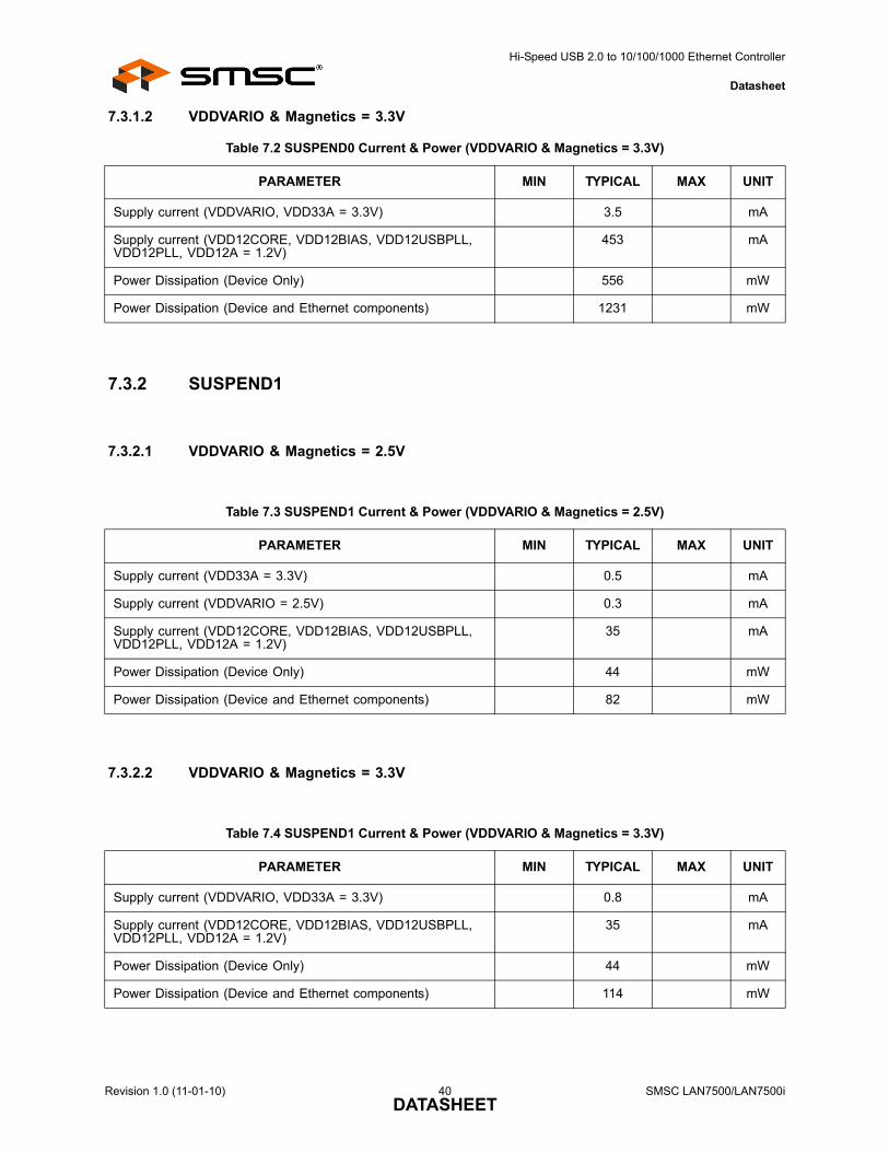
Hi-Speed USB 2.0 to 10/100/1000 Ethernet Controller
Datasheet
7.3.1.2 VDDVARIO & Magnetics = 3.3V
7.3.2 SUSPEND1
7.3.2.1 VDDVARIO & Magnetics = 2.5V
7.3.2.2 VDDVARIO & Magnetics = 3.3V
Table 7.2 SUSPEND0 Current & Power (VDDVARIO & Magnetics = 3.3V)
PARAMETER MIN TYPICAL MAX UNIT
Supply current (VDDVARIO, VDD33A = 3.3V) 3.5 mA
Supply current (VDD12CORE, VDD12BIAS, VDD12USBPLL, VDD12PLL, VDD12A = 1.2V)
453 mA
Power Dissipation (Device Only) 556 mW
Power Dissipation (Device and Ethernet components) 1231 mW
Table 7.3 SUSPEND1 Current & Power (VDDVARIO & Magnetics = 2.5V)
PARAMETER MIN TYPICAL MAX UNIT
Supply current (VDD33A = 3.3V) 0.5 mA
Supply current (VDDVARIO = 2.5V) 0.3 mA
Supply current (VDD12CORE, VDD12BIAS, VDD12USBPLL, VDD12PLL, VDD12A = 1.2V)
35 mA
Power Dissipation (Device Only) 44 mW
Power Dissipation (Device and Ethernet components) 82 mW
Table 7.4 SUSPEND1 Current & Power (VDDVARIO & Magnetics = 3.3V)
PARAMETER MIN TYPICAL MAX UNIT
Supply current (VDDVARIO, VDD33A = 3.3V) 0.8 mA
Supply current (VDD12CORE, VDD12BIAS, VDD12USBPLL, VDD12PLL, VDD12A = 1.2V)
35 mA
Power Dissipation (Device Only) 44 mW
Power Dissipation (Device and Ethernet components) 114 mW
Revision 1.0 (11-01-10) 40 SMSC LAN7500/LAN7500iDATASHEET
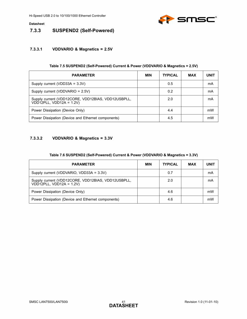
Hi-Speed USB 2.0 to 10/100/1000 Ethernet Controller
Datasheet
7.3.3 SUSPEND2 (Self-Powered)
7.3.3.1 VDDVARIO & Magnetics = 2.5V
7.3.3.2 VDDVARIO & Magnetics = 3.3V
Table 7.5 SUSPEND2 (Self-Powered) Current & Power (VDDVARIO & Magnetics = 2.5V)
PARAMETER MIN TYPICAL MAX UNIT
Supply current (VDD33A = 3.3V) 0.5 mA
Supply current (VDDVARIO = 2.5V) 0.2 mA
Supply current (VDD12CORE, VDD12BIAS, VDD12USBPLL, VDD12PLL, VDD12A = 1.2V)
2.0 mA
Power Dissipation (Device Only) 4.4 mW
Power Dissipation (Device and Ethernet components) 4.5 mW
Table 7.6 SUSPEND2 (Self-Powered) Current & Power (VDDVARIO & Magnetics = 3.3V)
PARAMETER MIN TYPICAL MAX UNIT
Supply current (VDDVARIO, VDD33A = 3.3V) 0.7 mA
Supply current (VDD12CORE, VDD12BIAS, VDD12USBPLL, VDD12PLL, VDD12A = 1.2V)
2.0 mA
Power Dissipation (Device Only) 4.6 mW
Power Dissipation (Device and Ethernet components) 4.6 mW
SMSC LAN7500/LAN7500i 41 Revision 1.0 (11-01-10)DATASHEET
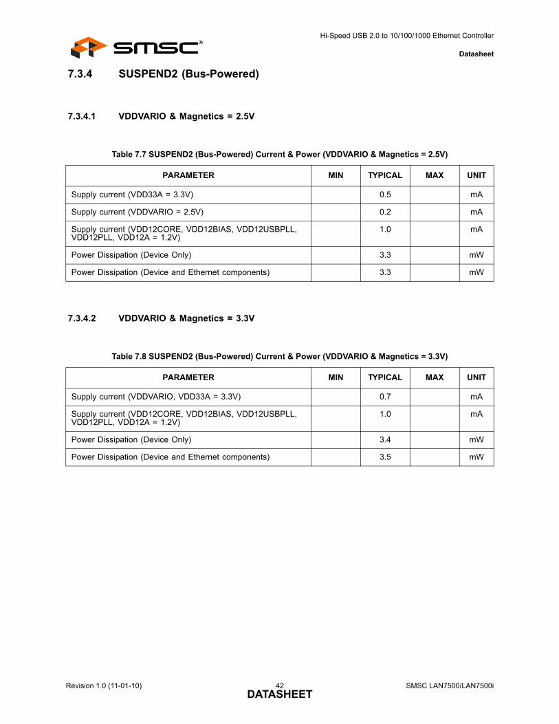
Hi-Speed USB 2.0 to 10/100/1000 Ethernet Controller
Datasheet
7.3.4 SUSPEND2 (Bus-Powered)
7.3.4.1 VDDVARIO & Magnetics = 2.5V
7.3.4.2 VDDVARIO & Magnetics = 3.3V
Table 7.7 SUSPEND2 (Bus-Powered) Current & Power (VDDVARIO & Magnetics = 2.5V)
PARAMETER MIN TYPICAL MAX UNIT
Supply current (VDD33A = 3.3V) 0.5 mA
Supply current (VDDVARIO = 2.5V) 0.2 mA
Supply current (VDD12CORE, VDD12BIAS, VDD12USBPLL, VDD12PLL, VDD12A = 1.2V)
1.0 mA
Power Dissipation (Device Only) 3.3 mW
Power Dissipation (Device and Ethernet components) 3.3 mW
Table 7.8 SUSPEND2 (Bus-Powered) Current & Power (VDDVARIO & Magnetics = 3.3V)
PARAMETER MIN TYPICAL MAX UNIT
Supply current (VDDVARIO, VDD33A = 3.3V) 0.7 mA
Supply current (VDD12CORE, VDD12BIAS, VDD12USBPLL, VDD12PLL, VDD12A = 1.2V)
1.0 mA
Power Dissipation (Device Only) 3.4 mW
Power Dissipation (Device and Ethernet components) 3.5 mW
Revision 1.0 (11-01-10) 42 SMSC LAN7500/LAN7500iDATASHEET
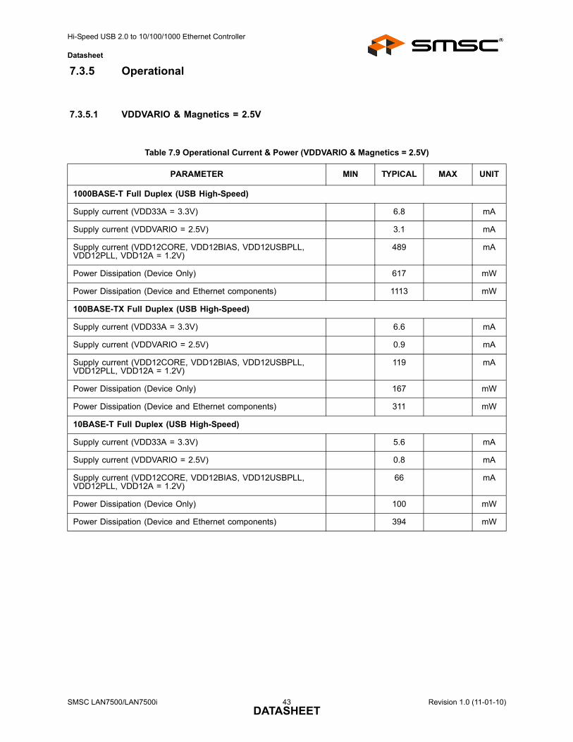
Hi-Speed USB 2.0 to 10/100/1000 Ethernet Controller
Datasheet
7.3.5 Operational
7.3.5.1 VDDVARIO & Magnetics = 2.5V
Table 7.9 Operational Current & Power (VDDVARIO & Magnetics = 2.5V)
PARAMETER MIN TYPICAL MAX UNIT
1000BASE-T Full Duplex (USB High-Speed)
Supply current (VDD33A = 3.3V) 6.8 mA
Supply current (VDDVARIO = 2.5V) 3.1 mA
Supply current (VDD12CORE, VDD12BIAS, VDD12USBPLL, VDD12PLL, VDD12A = 1.2V)
489 mA
Power Dissipation (Device Only) 617 mW
Power Dissipation (Device and Ethernet components) 1113 mW
100BASE-TX Full Duplex (USB High-Speed)
Supply current (VDD33A = 3.3V) 6.6 mA
Supply current (VDDVARIO = 2.5V) 0.9 mA
Supply current (VDD12CORE, VDD12BIAS, VDD12USBPLL, VDD12PLL, VDD12A = 1.2V)
119 mA
Power Dissipation (Device Only) 167 mW
Power Dissipation (Device and Ethernet components) 311 mW
10BASE-T Full Duplex (USB High-Speed)
Supply current (VDD33A = 3.3V) 5.6 mA
Supply current (VDDVARIO = 2.5V) 0.8 mA
Supply current (VDD12CORE, VDD12BIAS, VDD12USBPLL, VDD12PLL, VDD12A = 1.2V)
66 mA
Power Dissipation (Device Only) 100 mW
Power Dissipation (Device and Ethernet components) 394 mW
SMSC LAN7500/LAN7500i 43 Revision 1.0 (11-01-10)DATASHEET

Hi-Speed USB 2.0 to 10/100/1000 Ethernet Controller
Datasheet
7.3.5.2 VDDVARIO & Magnetics = 3.3V
Table 7.10 Operational Current & Power (VDDVARIO & Magnetics = 3.3V)
PARAMETER MIN TYPICAL MAX UNIT
1000BASE-T Full Duplex (USB High-Speed)
Supply current (VDDVARIO, VDD33A = 3.3V) 9.8 mA
Supply current (VDD12CORE, VDD12BIAS, VDD12USBPLL, VDD12PLL, VDD12A = 1.2V)
489 mA
Power Dissipation (Device Only) 620 mW
Power Dissipation (Device and Ethernet components) 1296 mW
100BASE-TX Full Duplex (USB High-Speed)
Supply current (VDDVARIO, VDD33A = 3.3V) 7.5 mA
Supply current (VDD12CORE, VDD12BIAS, VDD12USBPLL, VDD12PLL, VDD12A = 1.2V)
119 mA
Power Dissipation (Device Only) 168 mW
Power Dissipation (Device and Ethernet components) 379 mW
10BASE-T Full Duplex (USB High-Speed)
Supply current (VDDVARIO, VDD33A = 3.3V) 6.4 mA
Supply current (VDD12CORE, VDD12BIAS, VDD12USBPLL, VDD12PLL, VDD12A = 1.2V)
66 mA
Power Dissipation (Device Only) 101 mW
Power Dissipation (Device and Ethernet components) 512 mW
Revision 1.0 (11-01-10) 44 SMSC LAN7500/LAN7500iDATASHEET
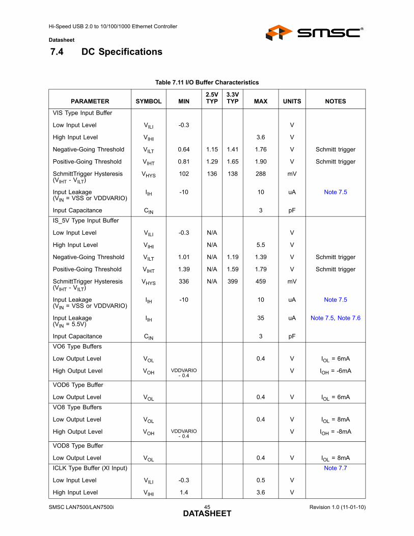
Hi-Speed USB 2.0 to 10/100/1000 Ethernet Controller
Datasheet
7.4 DC Specifications
Table 7.11 I/O Buffer Characteristics
PARAMETER SYMBOL MIN2.5V TYP
3.3V TYP MAX UNITS NOTES
VIS Type Input Buffer
Low Input Level
High Input Level
Negative-Going Threshold
Positive-Going Threshold
SchmittTrigger Hysteresis (VIHT - VILT)
Input Leakage(VIN = VSS or VDDVARIO)
Input Capacitance
VILI
VIHI
VILT
VIHT
VHYS
IIH
CIN
-0.3
0.64
0.81
102
-10
1.15
1.29
136
1.41
1.65
138
3.6
1.76
1.90
288
10
3
V
V
V
V
mV
uA
pF
Schmitt trigger
Schmitt trigger
Note 7.5
IS_5V Type Input Buffer
Low Input Level
High Input Level
Negative-Going Threshold
Positive-Going Threshold
SchmittTrigger Hysteresis (VIHT - VILT)
Input Leakage(VIN = VSS or VDDVARIO)
Input Leakage(VIN = 5.5V)
Input Capacitance
VILI
VIHI
VILT
VIHT
VHYS
IIH
IIH
CIN
-0.3
1.01
1.39
336
-10
N/A
N/A
N/A
N/A
N/A
1.19
1.59
399
5.5
1.39
1.79
459
10
35
3
V
V
V
V
mV
uA
uA
pF
Schmitt trigger
Schmitt trigger
Note 7.5
Note 7.5, Note 7.6
VO6 Type Buffers
Low Output Level
High Output Level
VOL
VOH VDDVARIO - 0.4
0.4 V
V
IOL = 6mA
IOH = -6mA
VOD6 Type Buffer
Low Output Level VOL 0.4 V IOL = 6mA
VO8 Type Buffers
Low Output Level
High Output Level
VOL
VOH VDDVARIO - 0.4
0.4 V
V
IOL = 8mA
IOH = -8mA
VOD8 Type Buffer
Low Output Level VOL 0.4 V IOL = 8mA
ICLK Type Buffer (XI Input)
Low Input Level
High Input Level
VILI
VIHI
-0.3
1.4
0.5
3.6
V
V
Note 7.7
SMSC LAN7500/LAN7500i 45 Revision 1.0 (11-01-10)DATASHEET
Hi-Speed USB 2.0 to 10/100/1000 Ethernet Controller
Datasheet
Note 7.5 This specification applies to all inputs and tri-stated bi-directional pins. Internal pull-downand pull-up resistors add +/- 50uA per-pin (typical).
Note 7.6 This is the total 5.5V input leakage for the entire device.
Note 7.7 XI can optionally be driven from a 25MHz single-ended clock oscillator.
Note 7.8 IEEE 802.ab Test Mode 1
Note 7.9 From 1/2 of average VOP, Test Mode 1
Note 7.10 IEEE 802.ab distortion processing
Note 7.11 Measured at line side of transformer, line replaced by 100Ω (+/- 1%) resistor.
Note 7.12 Offset from 16nS pulse width at 50% of pulse peak.
Note 7.13 Measured differentially.
Table 7.12 1000BASE-T Transceiver Characteristics
PARAMETER SYMBOL MIN TYP MAX UNITS NOTES
Peak Differential Output Voltage VOP 670 820 mV Note 7.8
Signal Amplitude Symmetry VSS 1 % Note 7.8
Signal Scaling VSC 2 % Note 7.9
Output Droop VOD 73.1 % Note 7.8
Transmission Distortion 10 mV Note 7.10
Table 7.13 100BASE-TX Transceiver Characteristics
PARAMETER SYMBOL MIN TYP MAX UNITS NOTES
Peak Differential Output Voltage High VPPH 950 - 1050 mVpk Note 7.11
Peak Differential Output Voltage Low VPPL -950 - -1050 mVpk Note 7.11
Signal Amplitude Symmetry VSS 98 - 102 % Note 7.11
Signal Rise and Fall Time TRF 3.0 - 5.0 nS Note 7.11
Rise and Fall Symmetry TRFS - - 0.5 nS Note 7.11
Duty Cycle Distortion DCD 35 50 65 % Note 7.12
Overshoot and Undershoot VOS - - 5 %
Jitter 1.4 nS Note 7.13
Revision 1.0 (11-01-10) 46 SMSC LAN7500/LAN7500iDATASHEET

Hi-Speed USB 2.0 to 10/100/1000 Ethernet Controller
Datasheet
Note 7.14 Min/max voltages guaranteed as measured with 100Ω resistive load.
7.5 AC Specifications
This section details the various AC timing specifications of the device.
Note: The USBDP and USBDM pin timing adheres to the USB 2.0 specification. Refer to theUniversal Serial Bus Revision 2.0 specification for detailed USB timing information.
Note: The Ethernet TX/RX pin timing adheres to the IEEE 802.3 specification. Refer to the IEEE802.3 specification for detailed Ethernet timing information.
7.5.1 Equivalent Test Load
Output timing specifications assume the 25pF equivalent test load illustrated in Figure 7.1 below,unless otherwise specified.
Table 7.14 10BASE-T Transceiver Characteristics
PARAMETER SYMBOL MIN TYP MAX UNITS NOTES
Transmitter Peak Differential Output Voltage VOUT 2.2 2.5 2.8 V Note 7.14
Receiver Differential Squelch Threshold VDS 300 420 585 mV
Figure 7.1 Output Equivalent Test Load
25 pF
OUTPUT
SMSC LAN7500/LAN7500i 47 Revision 1.0 (11-01-10)DATASHEET
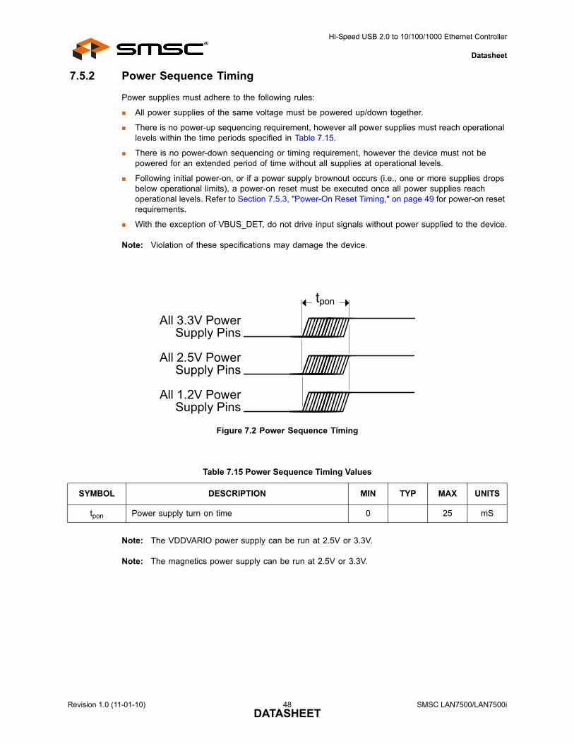
Hi-Speed USB 2.0 to 10/100/1000 Ethernet Controller
Datasheet
7.5.2 Power Sequence Timing
Power supplies must adhere to the following rules:
All power supplies of the same voltage must be powered up/down together.
There is no power-up sequencing requirement, however all power supplies must reach operational levels within the time periods specified in Table 7.15.
There is no power-down sequencing or timing requirement, however the device must not be powered for an extended period of time without all supplies at operational levels.
Following initial power-on, or if a power supply brownout occurs (i.e., one or more supplies drops below operational limits), a power-on reset must be executed once all power supplies reach operational levels. Refer to Section 7.5.3, "Power-On Reset Timing," on page 49 for power-on reset requirements.
With the exception of VBUS_DET, do not drive input signals without power supplied to the device.
Note: Violation of these specifications may damage the device.
Note: The VDDVARIO power supply can be run at 2.5V or 3.3V.
Note: The magnetics power supply can be run at 2.5V or 3.3V.
Figure 7.2 Power Sequence Timing
Table 7.15 Power Sequence Timing Values
SYMBOL DESCRIPTION MIN TYP MAX UNITS
tpon Power supply turn on time 0 25 mS
All 3.3V Power Supply Pins
All 2.5V Power Supply Pins
All 1.2V Power Supply Pins
tpon
Revision 1.0 (11-01-10) 48 SMSC LAN7500/LAN7500iDATASHEET
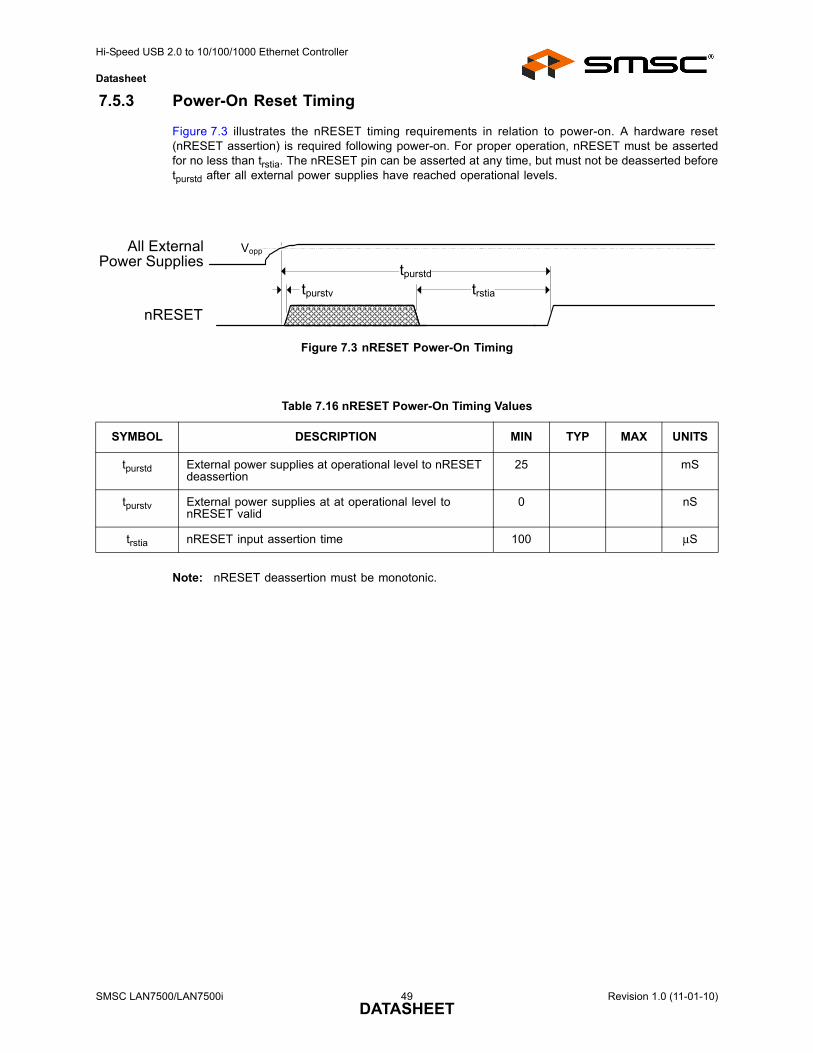
Hi-Speed USB 2.0 to 10/100/1000 Ethernet Controller
Datasheet
7.5.3 Power-On Reset Timing
Figure 7.3 illustrates the nRESET timing requirements in relation to power-on. A hardware reset(nRESET assertion) is required following power-on. For proper operation, nRESET must be assertedfor no less than trstia. The nRESET pin can be asserted at any time, but must not be deasserted beforetpurstd after all external power supplies have reached operational levels.
Note: nRESET deassertion must be monotonic.
Figure 7.3 nRESET Power-On Timing
Table 7.16 nRESET Power-On Timing Values
SYMBOL DESCRIPTION MIN TYP MAX UNITS
tpurstd External power supplies at operational level to nRESET deassertion
25 mS
tpurstv External power supplies at at operational level to nRESET valid
0 nS
trstia nRESET input assertion time 100 μS
nRESET
trstia
All External Power Supplies
tpurstd
Vopp
tpurstv
SMSC LAN7500/LAN7500i 49 Revision 1.0 (11-01-10)DATASHEET

Hi-Speed USB 2.0 to 10/100/1000 Ethernet Controller
Datasheet
7.5.4 Reset Timing
Figure 7.3 illustrates the nRESET pin timing requirements. When used, nRESET must be asserted forno less than trstia.
Note: A hardware reset (nRESET assertion) is required following power-on. Refer to Section 7.5.3,"Power-On Reset Timing," on page 49 for additional information.
Figure 7.4 nRESET Timing
Table 7.17 nRESET Timing Values
SYMBOL DESCRIPTION MIN TYP MAX UNITS
trstia nRESET input assertion time 1 μS
nRESET
trstia
Revision 1.0 (11-01-10) 50 SMSC LAN7500/LAN7500iDATASHEET
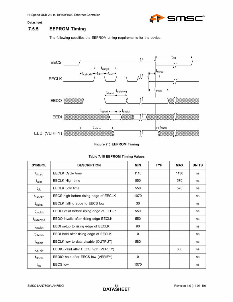
Hi-Speed USB 2.0 to 10/100/1000 Ethernet Controller
Datasheet
7.5.5 EEPROM Timing
The following specifies the EEPROM timing requirements for the device:
Figure 7.5 EEPROM Timing
Table 7.18 EEPROM Timing Values
SYMBOL DESCRIPTION MIN TYP MAX UNITS
tckcyc EECLK Cycle time 1110 1130 ns
tckh EECLK High time 550 570 ns
tckl EECLK Low time 550 570 ns
tcshckh EECS high before rising edge of EECLK 1070 ns
tcklcsl EECLK falling edge to EECS low 30 ns
tdvckh EEDO valid before rising edge of EECLK 550 ns
tckhinvld EEDO invalid after rising edge EECLK 550 ns
tdsckh EEDI setup to rising edge of EECLK 90 ns
tdhckh EEDI hold after rising edge of EECLK 0 ns
tckldis EECLK low to data disable (OUTPUT) 580 ns
tcshdv EEDIO valid after EECS high (VERIFY) 600 ns
tdhcsl EEDIO hold after EECS low (VERIFY) 0 ns
tcsl EECS low 1070 ns
EECLK
EEDO
EEDI
EECS
tckldis
tcshckh
EEDI (VERIFY)
tckh tckl
tckcyc tcklcs
l
tcsl
tdvckhtckhinvld
tdsckh tdhckh
tdhcsltcshdv
SMSC LAN7500/LAN7500i 51 Revision 1.0 (11-01-10)DATASHEET
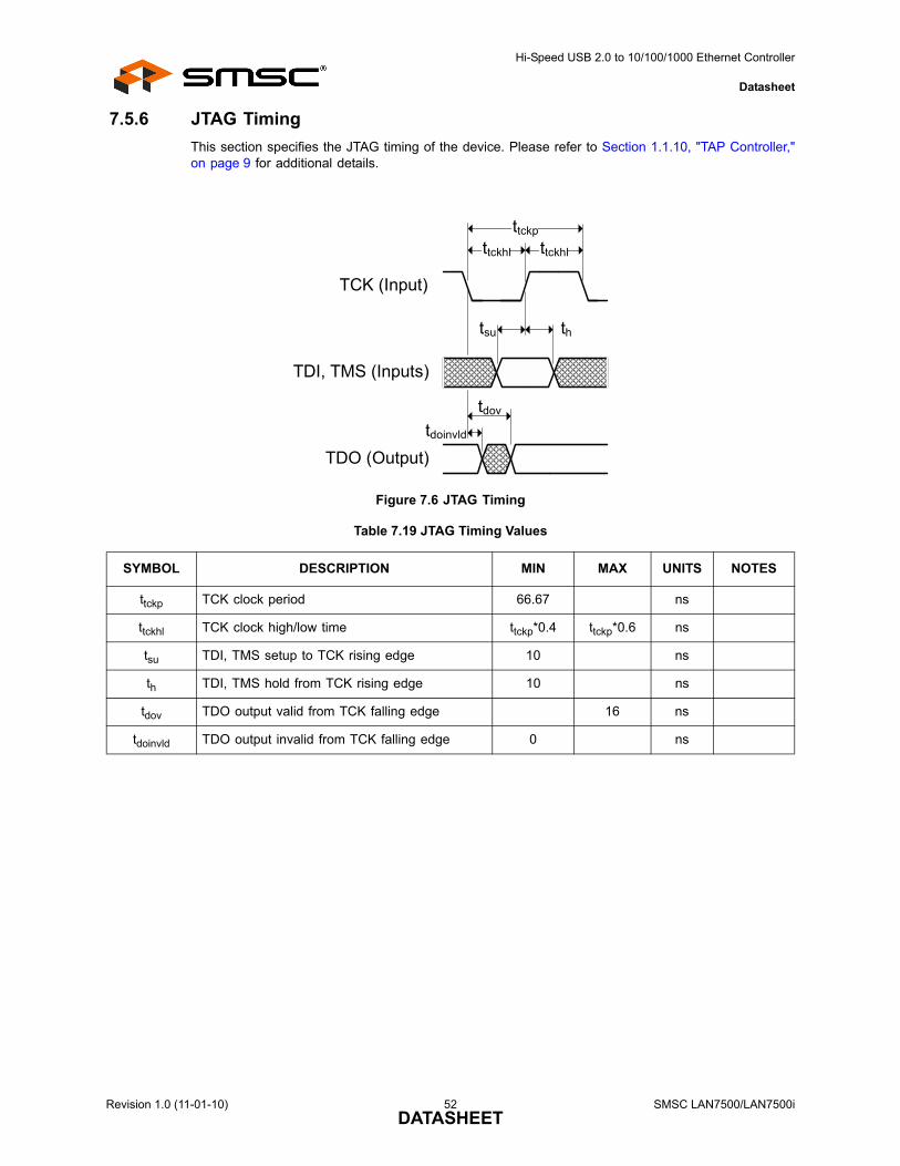
Hi-Speed USB 2.0 to 10/100/1000 Ethernet Controller
Datasheet
7.5.6 JTAG Timing
This section specifies the JTAG timing of the device. Please refer to Section 1.1.10, "TAP Controller,"on page 9 for additional details.
Figure 7.6 JTAG Timing
Table 7.19 JTAG Timing Values
SYMBOL DESCRIPTION MIN MAX UNITS NOTES
ttckp TCK clock period 66.67 ns
ttckhl TCK clock high/low time ttckp*0.4 ttckp*0.6 ns
tsu TDI, TMS setup to TCK rising edge 10 ns
th TDI, TMS hold from TCK rising edge 10 ns
tdov TDO output valid from TCK falling edge 16 ns
tdoinvld TDO output invalid from TCK falling edge 0 ns
TCK (Input)
TDI, TMS (Inputs)
ttckhl
ttckp
ttckhl
tsu th
tdov
TDO (Output)
tdoinvld
Revision 1.0 (11-01-10) 52 SMSC LAN7500/LAN7500iDATASHEET
Hi-Speed USB 2.0 to 10/100/1000 Ethernet Controller
Datasheet
7.6 Clock Circuit
The device can accept either a 25MHz crystal (preferred) or a 25MHz single-ended clock oscillator (+/-50ppm) input. If the single-ended clock oscillator method is implemented, XO should be leftunconnected and XI should be driven with a nominal 0-3.3V clock signal. The input clock duty cycleis 40% minimum, 50% typical and 60% maximum.
It is recommended that a crystal utilizing matching parallel load capacitors be used for the crystalinput/output signals (XI/XO). See Table 7.20 for the recommended crystal specifications.
Note 7.15 The maximum allowable values for Frequency Tolerance and Frequency Stability areapplication dependant. Since any particular application must meet the IEEE +/-50 PPMTotal PPM Budget, the combination of these two values must be approximately +/-45 PPM(allowing for aging).
Note 7.16 Frequency Deviation Over Time is also referred to as Aging.
Note 7.17 The total deviation for the Transmitter Clock Frequency is specified by IEEE 802.3u as +/- 50 PPM.
Note 7.18 0oC for commercial version, -40oC for industrial version.
Note 7.19 +70oC for commercial version, +85oC for industrial version.
Note 7.20 This number includes the pad, the bond wire and the lead frame. PCB capacitance is notincluded in this value. The XO/XI pin and PCB capacitance values are required toaccurately calculate the value of the two external load capacitors. These two external loadcapacitors determine the accuracy of the 25.000 MHz frequency.
Table 7.20 LAN7500/LAN7500i Crystal Specifications
PARAMETER SYMBOL MIN NOM MAX UNITS NOTES
Crystal Cut AT, typ
Crystal Oscillation Mode Fundamental Mode
Crystal Calibration Mode Parallel Resonant Mode
Frequency Ffund - 25.000 - MHz
Frequency Tolerance @ 25oC Ftol - - +/-50 PPM Note 7.15
Frequency Stability Over Temp Ftemp - - +/-50 PPM Note 7.15
Frequency Deviation Over Time Fage - +/-3 to 5 - PPM Note 7.16
Total Allowable PPM Budget - - +/-50 PPM Note 7.17
Shunt Capacitance CO - 7 typ - pF
Load Capacitance CL - 20 typ - pF
Drive Level PW 300 - - uW
Equivalent Series Resistance R1 - - 50 Ohm
Operating Temperature Range Note 7.18 - Note 7.19 oC
LAN7500/LAN7500i XI Pin Capacitance
- 3 typ - pF Note 7.20
LAN7500/LAN7500i XO Pin Capacitance
- 3 typ - pF Note 7.20
SMSC LAN7500/LAN7500i 53 Revision 1.0 (11-01-10)DATASHEET
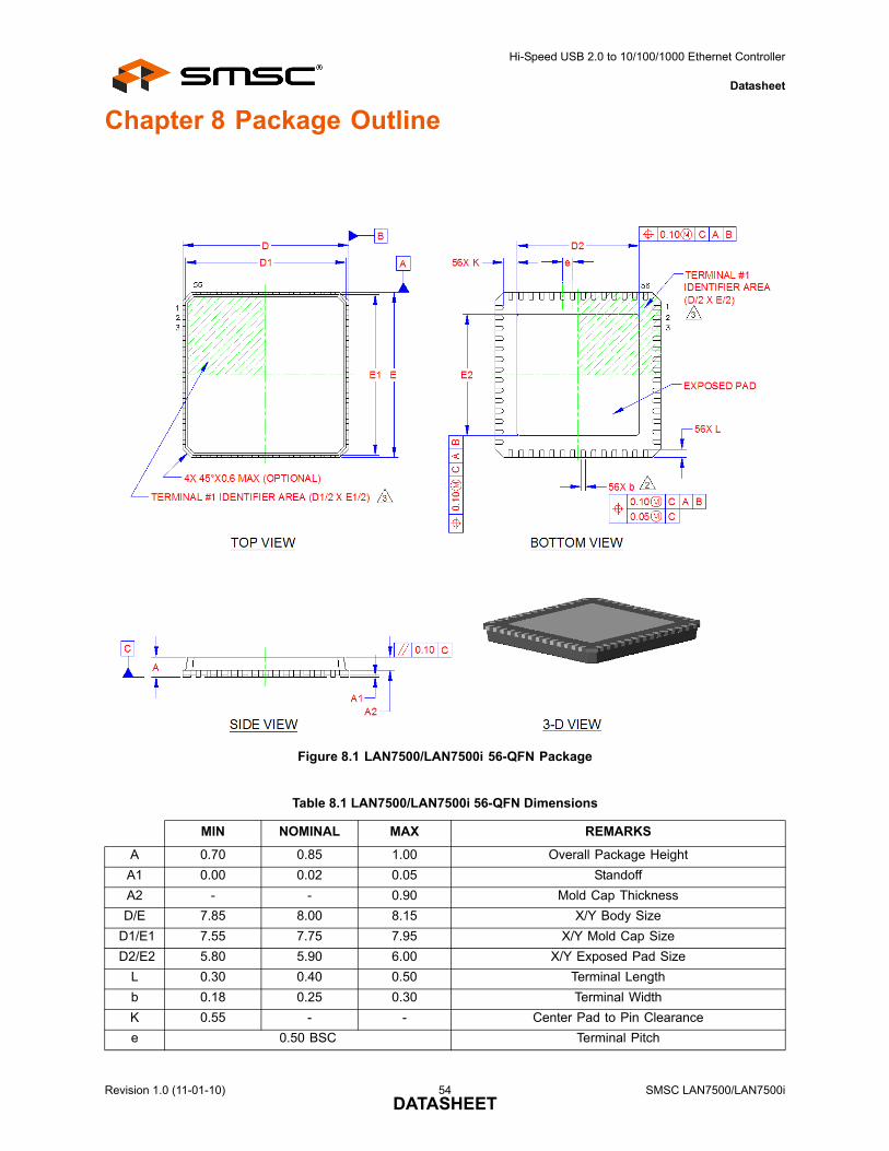
Hi-Speed USB 2.0 to 10/100/1000 Ethernet Controller
Datasheet
Chapter 8 Package Outline
Figure 8.1 LAN7500/LAN7500i 56-QFN Package
Table 8.1 LAN7500/LAN7500i 56-QFN Dimensions
MIN NOMINAL MAX REMARKS
A 0.70 0.85 1.00 Overall Package Height
A1 0.00 0.02 0.05 Standoff
A2 - - 0.90 Mold Cap Thickness
D/E 7.85 8.00 8.15 X/Y Body Size
D1/E1 7.55 7.75 7.95 X/Y Mold Cap Size
D2/E2 5.80 5.90 6.00 X/Y Exposed Pad Size
L 0.30 0.40 0.50 Terminal Length
b 0.18 0.25 0.30 Terminal Width
K 0.55 - - Center Pad to Pin Clearance
e 0.50 BSC Terminal Pitch
Revision 1.0 (11-01-10) 54 SMSC LAN7500/LAN7500iDATASHEET
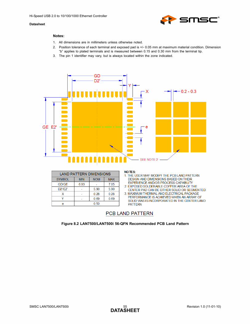
Hi-Speed USB 2.0 to 10/100/1000 Ethernet Controller
Datasheet
Notes:
1. All dimensions are in millimeters unless otherwise noted.
2. Position tolerance of each terminal and exposed pad is +/- 0.05 mm at maximum material condition. Dimension“b” applies to plated terminals and is measured between 0.15 and 0.30 mm from the terminal tip.
3. The pin 1 identifier may vary, but is always located within the zone indicated.
Figure 8.2 LAN7500/LAN7500i 56-QFN Recommended PCB Land Pattern
SMSC LAN7500/LAN7500i 55 Revision 1.0 (11-01-10)DATASHEET
Hi-Speed USB 2.0 to 10/100/1000 Ethernet Controller
Datasheet
Revision 1.0 (11-01-10) 56 SMSC LAN7500/LAN7500iDATASHEET
Chapter 9 Revision History
Table 9.1 Customer Revision History
REVISION LEVEL AND DATE SECTION/FIGURE/ENTRY CORRECTION
Rev. 1.0(11-01-10)
All Initial Release.