laboratory manual - jawaharlal nehru engineering college lab-manual.pdf · laboratory manual linear...
TRANSCRIPT
Jawaharlal Nehru Engineering College
Laboratory Manual
LINEAR INTEGRATED CIECUITS & APPLICATIONS
For
Second Year Students
Author JNEC INSTRU DEPT., Aurangabad

SUBJECT INDEX
1. Non-Inverting Amplifier with feedback.
2. Inverting Amplifier with feedback.
3. Differential Amplifier.
4. Summing Amplifier.
5. Integrator circuit.
6. Differentiation Amplifier.
7. First order low-pass filter.
8. First order high-pass filter.
9. Wein bridge oscillator.
10. Triangular wave generator.
11. Schmitt trigger.
12. Monostable multivibrator using IC 555.
13. Astable multivibrator using IC 555.

EXPERIMENT NO.1
Non-Inverting Amplifier with feedback. OBJECTIVE: To Study op-amp 741 IC as a non-inverting amplifier with feedback. EXPERIMENTAL SET-UP:
Accessories:
Power Supply ± 12V Input Supply (0-5V) CRO Bread Board, connecting wires, Signal generator for a.c. signal Components:
IC741 Resistors, R1 = 1KΩ/0.25W/10% RF = 10KΩ/0.25W/10% CIRCUIT DIAGRAM:

THEORY:
Figure shows a non-inverting amplifier. The o/p Voltage Vo is of the same polarity as the input voltage Vin. The input resistance of the non-inverting amplifier is very large (100MΩ) in this case. The input signal is applied directly to the non-inverting (+ve) input terminal of the amplifier and the feedback resistance are connected between the output terminal, the –ve input terminal and ground.
The Minimum Gain of the Non-Inverting Amplifier is 1.
Closed –Loop Voltage Gain (AF):
AF = Vo/Vin However, Vo = A (V1 – V2) Referring to figure, V1 = Vin V2 = Vf = R1Vo since Ri >>> R1 (R1 + RF) Therefore, Vo = A( Vin - R1Vo ) (R1 + RF) Rearranging, we get Vo = A(R1 +RF)Vin R1 + RF + AR1 Thus AF = Vo = A(R1 +RF)
Vin R1 + RF + AR1 Generally A is very large (typically 105). Therefore AR1>>(R1 + RF) and (R1 + RF + AR1) ≈ AR1 Thus AF = Vo = 1 + RF (ideal) Vin R1 PROCEDURE:
1. Make the connections as per the circuit diagram. 2. Apply the i/p to the Non-Inverting terminal and obtain the output on the CRO. 3. Take various readings by varying the input voltage and hence calculate the gain. 4. Calculate the gain using formula.
AF = 1 + RF (Theoretical)
R1
AF = Vo (Practical) Vin

OBSERVATION TABLE:
Sr. No.
Vin (Volts)
Vo (Volts)
AF = 1 + (RF/R1) (Theoretical)
AF = Vo/Vin (Practical)
1. 2. 3. 4.
RESULT:
Voltage Gain of the Non-Inverting amplifier is always greater than unity. The Theoretical and Practical values of the Gain are nearly matching.
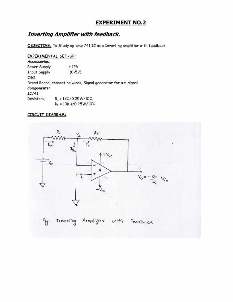
EXPERIMENT NO.2
Inverting Amplifier with feedback. OBJECTIVE: To Study op-amp 741 IC as a Inverting amplifier with feedback. EXPERIMENTAL SET-UP:
Accessories:
Power Supply ± 12V Input Supply (0-5V) CRO Bread Board, connecting wires, Signal generator for a.c. signal Components:
IC741 Resistors, R1 = 1KΩ/0.25W/10% RF = 10KΩ/0.25W/10% CIRCUIT DIAGRAM:

THEORY:
Figure shows a inverting amplifier. The o/p Voltage Vo is of the opposite polarity as the input voltage Vin. The input signal is applied directly to the inverting (-ve) input terminal of the amplifier and the feedback resistance is also connected between the output terminal, the –ve input terminal and ground.
The Gain of the Inverting Amplifier can be set below unity i.e. 1. Hence the inverting amplifier configuration with feedbacks lends itself to a majority of applications as against those of the non-inverting amplifier.
Closed –Loop Voltage Gain (AF):
The closed-loop voltage gain AF can be obtained by writing Kirchoff’s Current equation at the input node V2 as follows: Iin = IF + IB ………………….(1) Since Ri is very large, the input bias current IB is negligibly small. For instance,
Ri = 2MΩ and IB = 0.5µA for 741C. Therefore, Iin ≅ IF
That is, Vin – V2 = V2 – Vo ……………(2) R1 RF However, V1 – V2 = Vo/A Since V1 = 0V, V2 = –Vo/A Substituting this value of V2 in Equation (2)
Vin + Vo/A = –(Vo/A) – Vo R1 RF AF = Vo = − ARF ……………………(3) Vin R1 + RF + AR1
Since the internal gain A of op-amp is very large (ideally infinity), AR1 >> R1 + RF. Therefore equ. (3) can be rewritten as,
AF = Vo = −−−− RF (ideal) Vin R 1
PROCEDURE:
1. Make the connections as per the circuit diagram. 2. Apply the i/p to the Inverting terminal and obtain the output on the CRO. 3. Take various readings by varying the input voltage and hence calculate the gain. 4. Calculate the gain using formula.
AF = −−−− RF (Theoretical)
R1
AF = Vo (Practical) Vin

OBSERVATION TABLE:
Sr. No.
Vin (Volts)
Vo (Volts)
AF = −−−− (RF/R1) (Theoretical)
AF = Vo/Vin (Practical)
1. 2. 3. 4.
RESULT:
Voltage Gain of the Inverting amplifier depends only on the feedback components and is independent of the internal gain ‘A’ of the op-amp. The value of AF can be less than unity. The Theoretical and Practical values of the Gain are nearly matching.

EXPERIMENT NO.3
Differential Amplifier. OBJECTIVE: To construct a Subtractor amplifier using a basic Differential amplifier Configuration. EXPERIMENTAL SET-UP:
Accessories:
Power Supply ±12V Input Supply (2) (0-5V) CRO Bread Board, connecting wires, Signal generator for a.c. signal Components:
IC741 Resistors, R1 = 10KΩ/0.25W/10% R2 = 10KΩ/0.25W/10% R3 = 10KΩ/0.25W/10% RF = 10KΩ/0.25W/10% CIRCUIT DIAGRAM:

THEORY:
Figure shows a Differential amplifier as a subtractor. In subtractor circuit all the external resistors are made equal in value, so the gain of the amplifier is 1.This circuit is also called scaling amplifier.
The differential amplifier are used in instrumentation and industrial applications to amplify differences between two input signals, such as the outputs of the wheatstone bridge circuits. Differential amplifier are preferred because they are better able to reject common-mode (noise) voltages than single i/p ckts. Such as inverting and non-inverting amplifiers. They also present a balanced input impedance.
Output Voltage (Vo):
The circuit in figure has two inputs, Vx and Vy. Using superposition theorem to establish relationship between i/p amd o/p.
When, Vy = 0V,the configuration becomes an inverting amplifier, hence the o/p due to Vx only is, Vox = − RF (Vx) …………………….(1) R1 Similarly, when Vx =0, the configuration becomes an non-inverting amplifier having a voltage-
divider network composed of R2 and R3 at the non-inverting input. Therefore, V1 = R3 (Vy) ………………………………(2) R2 + R3
And the output due to Vy then is Voy = ( 1 + RF ) V1
R1 That is, Voy = __R3 ( R1 + RF )Vy R2 +R3 R1 Since R1=R2 and RF = R3, Voy = RF (Vy) ………………………(3)
R1 Thus from equations (1) and (3), the net output voltage is, Vo = Vox + Voy Vo = – RF (Vx – Vy) = – RF(Vxy) ……………………….(4 ) R1 R1 Or the voltage gain AD = Vo = – RF
Vxy R1
Where, Vxy = Vx – Vy
Now, if RF = R1
Therefore, from equation (4)

Vo = – (Vx – Vy)
That is, Vo = Vy –Vx ………………………………….. (5) PROCEDURE:
1. Make the connections as per the circuit diagram. 2. Apply the i/p to the Inverting terminal and non-inverting terminal obtain the output on the
CRO. 3. Take various readings by varying the input voltages and hence calculate the output voltage.
Vo = Vy –Vx
OBSERVATION TABLE:
Sr. No.
Vx (Volts)
Vy (Volts)
Vo = Vy –Vx
Vo on CRO
1. 2. 3. 4.
RESULT:
Output Voltage Differential amplifier is the difference in the voltage between Non-Inverting and Inverting terminals. And the output voltage on the CRO is nearly equal to the calculated difference voltage applied at the input.

EXPERIMENT NO.4
Summing Amplifier. OBJECTIVE: To Verify a Non-Inverting Summing Amplifier. EXPERIMENTAL SET-UP:
Accessories:
Power Supply ±12V Input Supply (3) (0-5V) CRO Bread Board, connecting wires, Signal generator for a.c. signal Components:
IC741 Resistors, R1 = 5KΩ/0.25W/10% R2 = 6.8KΩ/0.25W/10% R3 = 6.8KΩ/0.25W/10% R4 = 6.8KΩ/0.25W/10% RF = 10KΩ/0.25W/10% CIRCUIT DIAGRAM:

THEORY: The circuit diagram is as shown in the figure. The circuit can be used as a summing amplifier by making Gain i.e. 1+ RF/R1 equal to number of inputs.
Output Voltage (Vo):
By using superposition theorem at node V1 at Non-Inverting Terminal, V1 = R/2 Va + R/2 Vb + R/2 Vc R + R/2 R + R/2 R + R/2 Or V1 = Va + Vb + Vc = Va + Vb + Vc 3 3 3 3 Hence the output voltage Vo is, Vo = ( 1 + RF/R1 ) V1 Therefore, Vo = (1 + RF ) Va + Vb + Vc R1 3 Now, if RF = 2R1 Then Vo = Va + Vb + Vc
PROCEDURE:
1. Make the connections as per the circuit diagram. 2. Apply three i/p voltageto the Non-Inverting terminal and ground the Inverting terminal. 3. Take the output on CRO by varying the input voltages. 4. Calculate the output voltage.
Vo = Va +Vb +Vc.
5. Compare the results.
OBSERVATION TABLE:
Sr. No.
Va (Volts)
Vb (Volts)
Vc (Volts)
Vo = Va +Vb+ Vc
Vo on CRO
1. 2. 3. 4.
RESULT:
Output Voltage of Summing or Scaling amplifier is the sum of voltages applied at the non-inverting terminals. And the output voltage on the CRO is nearly equal to the calculated difference voltage applied at the input.

EXPERIMENT NO.5
Integration Amplifier. OBJECTIVE: To Verify the Integrator circuit. EXPERIMENTAL SET-UP:
Accessories:
Power Supply ±12V Input Supply (1) (0-5V) CRO Bread Board, connecting wires, and Signal generator for a.c. signal Components:
IC741 Resistors, R1 = 1KΩ/0.25W/10% RF = 10KΩ/0.25W/10% C = 0.01µF CIRCUIT DIAGRAM:

THEORY:
The circuit in which the output waveform is the integral of the input voltage waveform is the integrator or the integration amplifier. Such a circuit is obtained by using a basic inverting amplifier configuration if the feedback resistor RF is replaced by a capacitor CF.
Output Voltage (Vo):
Applying KCL at node V2: I1 = IB + IF Since IB is negligibly small, I1 ≅ IF Current through and voltage across capacitor is, Ic = C dVc dt Therefore, Vin – V2 = CF (d/dt) (V2-Vo) R1 However, V1 =V2 ≅ 0 because A is very large. Therefore, Vin = CF d (–Vo) R1 dt The output voltage can be obtained by integrating both sides with respect to time: ∫ Vin dt = ∫ CF d (–Vo) dt
R1 dt = CF (-Vo) + Vo Therefore, Vo = – 1 ∫ Vin dt + C R1 CF Where C is the integration constant and is proportional to the value of the output voltage Vo at time t = 0 seconds. The frequency at which the Gain is 0 dB is, fb = 1/2πR1CF Both the stability and the low-frequency roll-off can be corrected by the addition of a resistor RF. The Gain limiting frequency fa is given by, fa = 1/2πRFCF PROCEDURE:
1. Make the connections as per the circuit diagram. 2. Take RF = 10R1 3. Try to make time constant RFCF = 1. 4. Apply i/p voltage to the Inverting terminal and ground the Non-Inverting terminal. 5. Take the output on CRO by varying the input voltages. 6. Calculate the output voltage.
Vo = – 1 ∫∫∫∫ Vin dt + C
R1 CF
7. Compare the results.

OBSERVATION TABLE:
Sr. No.
Vin (Volts)
Vo calculated
Vo on CRO
1. 2. 3. 4.
RESULT:
Output Voltage is directly proportional to the –ve integral of input voltage and inversely proportional to the time constant R1CF. And the output voltage on the CRO is nearly equal to the calculated difference voltage applied at the input.

EXPERIMENT NO.6
Differentiation Amplifier. OBJECTIVE: To Verify the Differentiation circuit. EXPERIMENTAL SET-UP:
Accessories:
Power Supply ±12V Input Supply (1) (0-5V) CRO Bread Board, connecting wires, and Signal generator for a.c. signal Components:
IC741 Resistors, R1 = 82Ω RF = 1.5KΩ C1 = 0.1µF CF = 0.05µF

CIRCUIT DIAGRAM:

THEORY:
The circuit in which the output waveform is the derivative of the input voltage waveform is the differentiator or differentiation amplifier. Such a circuit is obtained by using a basic inverting amplifier configuration if the input resistor R1 is replaced by a capacitor C1.
Output Voltage (Vo):
Applying KCL at node V2: IC = IB + IF Since IB is negligibly small, IC = IF Current through and voltage across capacitor is, C1 d (Vin – Vo) = V2 – Vo dt RF However, V1 =V2 ≅ 0V because A is very large. Therefore, C1d (Vin) = –Vo/RF dt or Vo = –RFC1d Vin dt The frequency at which the Gain is 0 dB is, fa = 1/2πRFC1 Both the stability and the low-frequency roll-off can be corrected by the addition of a resistor RF. The Gain limiting frequency fa is given by, fb = 1/2πR1C1 Where R1C1 = RFCF
PROCEDURE: 1. Make the connections as per the circuit diagram. 2. Try for time constant RFCF = R1C1. 3. Apply i/p voltage to the Inverting terminal and ground the Non-Inverting terminal. 4. Take the output on CRO by varying the input voltages. 5. Calculate the output voltage.
Vo = –RFC1 d Vin
dt
6. Compare the results.

OBSERVATION TABLE:
Sr. No.
Vin (Volts)
Vo calculated
Vo on CRO
1. 2. 3. 4.
RESULT:
Output Voltage Vo is equal to RFC1 times negative instantaneous rate of change of voltage with respect to differentiator circuit.

EXPERIMENT NO. 7
First order Low-Pass filter. OBJECTIVE: To Design a First order Low-Pass Butterworth filter. EXPERIMENTAL SET-UP:
Accessories:
Power Supply ±12V Input Supply (1) (0-5V) CRO Bread Board, connecting wires, and Signal generator for a.c. signal Components:
IC741 Resistors, R1 = 10KΩ RF = 10KΩ Pot = 20KΩ C = 0.01µF CIRCUIT DIAGRAM:

THEORY:
A low pass filter has a constant gain from 0Hz ta a high cutoff frequency fH. Therefore the bandwidth is also fH. At fH the Gain is down by 3 dB ; after that (f > fH) it decreases with the increase in input frequency. The frequency between 0Hz and fH are known as the passband frequencies, whereas the range of frequencies, those beyond fH, that are attenuated includes the stopband frequencies. First order low-pass Butterworth filter uses an RC network for filtering. Note that the op-amp is used in the noninverting configuration; hence it does not load down the RC network. Resistors R1 and RF determine the Gain of the filter. Vo = ( 1 + RF ) V1 R1 AF = (1 + RF ) R1 Vo = AF …………………………(1) Vin 1 + j(f/fH) Where, Vo/Vin = gain of the filter as a function of the frequency AF = 1 + RF/R1 = Passband Gain of the filter. f = frequency of the input signal fH = 1/2πRC = High cutoff frequency of the filter
The Gain magnitude and phase angle equations of the low-pass filter can be obtained by converting Equation (1) in equivalent polar form, as follows:
Magnitude, Vo = . AF Vin √ 1+ (f/fH)2 Ǿ = – tan-1( f/fH )
Where Ǿ is phase angle in degrees.
PROCEDURE:
1. Make the connections as per the circuit diagram. 2. Choose a value of high cutoff frequency fH. 3. Select a value of C less than or equal to 1µF. 4. Calculate the value of R using,
R = 1
2ππππfHC 5. Finally select values of R1 and RF dependent on the desired pass band gain AF using,
AF = 1 +RF
R1

OBSERVATION TABLE:
Sr. No.
Vin (Volts)
Vo = . AF Vin √ 1+ (f/fH)2
Ǿ = – tan-1( f/fH )
1. 2. 3. 4.
RESULT:
Thus the low-pass filter has a constant gain AF from 0Hz to the high cutoff frequency fH.

EXPERIMENT NO. 8
First order High-Pass filter. OBJECTIVE: To Design a First order High-Pass Butterworth filter. EXPERIMENTAL SET-UP:
Accessories:
Power Supply ±12V Input Supply (1) (0-5V) CRO Bread Board, connecting wires, and Signal generator for a.c. signal Components:
IC741 Resistors, R1 = 10KΩ RF = 10KΩ Pot = 20KΩ C = 0.01µF CIRCUIT DIAGRAM:

THEORY:
A High pass filter has a stopband 0 < f < fL and a passband f > fL. FL is the low cutoff frequency, and f is the operating frequency. Vo = ( 1 + RF ) j2πfRC Vin R1 1 + j2πfRC AF = ( 1 + RF ) R1 Vo = A ( j (f/fL) ) …………………………(1) Vin 1 + j (f/fL) Where, Vo/Vin = gain of the filter as a function of the frequency AF = 1 + RF/R1 = Passband Gain of the filter. f = frequency of the input signal (Hz) fL = 1/2πRC = Low cutoff frequency of the filter (Hz)
The Gain magnitude and phase angle equations of the High-pass filter can be obtained by converting Equation (1) in equivalent polar form, as follows:
Magnitude, Vo = . AF(f/fL) Vin √ 1+ (f/fL)2 Ǿ = – tan-1( f/fL )
Where Ǿ is phase angle in degrees.
PROCEDURE: 1. Make the connections as per the circuit diagram. 2. Choose a value of high cutoff frequency fL. 3. Select a value of C less than or equal to 1µF. 4. Calculate the value of R using,
R = 1
2ππππfLC 5. Finally select values of R1 and RF dependent on the desired passband gain AF using,
AF = 1 +RF
R1

OBSERVATION TABLE:
Sr. No.
Vin (Volts)
Vo = . AF(f/fL) Vin √ 1+ (f/fL)2
Ǿ = – tan-1( f/fL )
1. 2. 3. 4.
RESULT:
Thus the High-pass filter has a constant gain AF from low cutoff frequency, fL.

EXPERIMENT NO. 9
Wein Bridge Oscillator. OBJECTIVE: To Design a Wein Bridge Oscillator. EXPERIMENTAL SET-UP:
Accessories:
Power Supply ±12V CRO Bread Board, connecting wires, and Signal generator for a.c. signal Components:
IC741 Resistors, R1 = 12KΩ RF = 50KΩ Pot at 25 KΩ
R = 3.3KΩ 2 No. C = 0.05µF 2 No.
CIRCUIT DIAGRAM:

THEORY: Because of its simplicity and stability, one of the most commonly used audio-frequency oscillators is the wein bridge. In circuit the wein bridge circuit is connected between the amplifier input terminals and the output terminal. The bridge has a series RC network in one arm and a parallel RC network in the adjoining arm. In the remaining two arms of the bridge, resistors R1 and RF are connected. The phase angle criterion is that the total phase shift around the circuit must be 0o. This condition occurs only when the bridge is balanced, that is, at resonance. The frequency of Oscillation fo is exactly the resonant frequency of the balanced Wein bridge and is given by fo = . 1 . = 0.159 2πfRC RC Assuming that the resistors are equal in value, and capacitors are equal in value in the reactive leg of the Wein bridge. At this frequency the gain required for sustained oscillation is given by, Av = 1 = 3 B That is, 1 + RF = 3 R1 Or RF = 2R1 PROCEDURE:
1. Make the connections as per the circuit diagram. 2. Select RF = 2R1 for resonance frequency. 3. Take the output on CRO. 4. Calculate the practical frequency by the waveform on CRO. 5. Calculate the theoretical frequency.
CONCLUSION:
Thus we have studied Wein Bridge Oscillator.

EXPERIMENT NO. 10
Triangular wave generator. OBJECTIVE: To Design a Triangular wave generator. EXPERIMENTAL SET-UP:
Accessories:
Power Supply ±15V 2 No. CRO Bread Board, connecting wires, and Signal generator for a.c. signal Components:
Dual Op-amp: 1458/353 Resistors, R = 10KΩ R1 = 10KΩ R2 = 20KΩ pot 11.6KΩ
R3 = 100KΩ R4 = 10 R3
ROM =100KΩ C = 0.05µF C2 = 0.01µF
CIRCUIT DIAGRAM:

THEORY:
A Triangular Waveform can be formed by connecting an integrator to the square wave generator. The frequencies of the square wave and the triangular wave are same. For fixed R1, R2 and C values, the frequency of the square wave as well as the triangular wave depends on the resistance R. As R is increased or decreased, the frequency of the square wave and triangular wave will increase or decrease respectively. Although the Amplitude of the square wave is constant ( ± Vsat ) , the Amplitude of the triangular wave decreases with an increase in its frequency, and vice versa. PROCEDURE:
1. Make the connections as per the circuit diagram. 2. Take the output on CRO. 3. Note +Vsat and –Vsat. 4. Note the Amplitude and frequency of triangular wave.
CONCLUSION:
Thus we have observed the output of the Triangular wave generator.
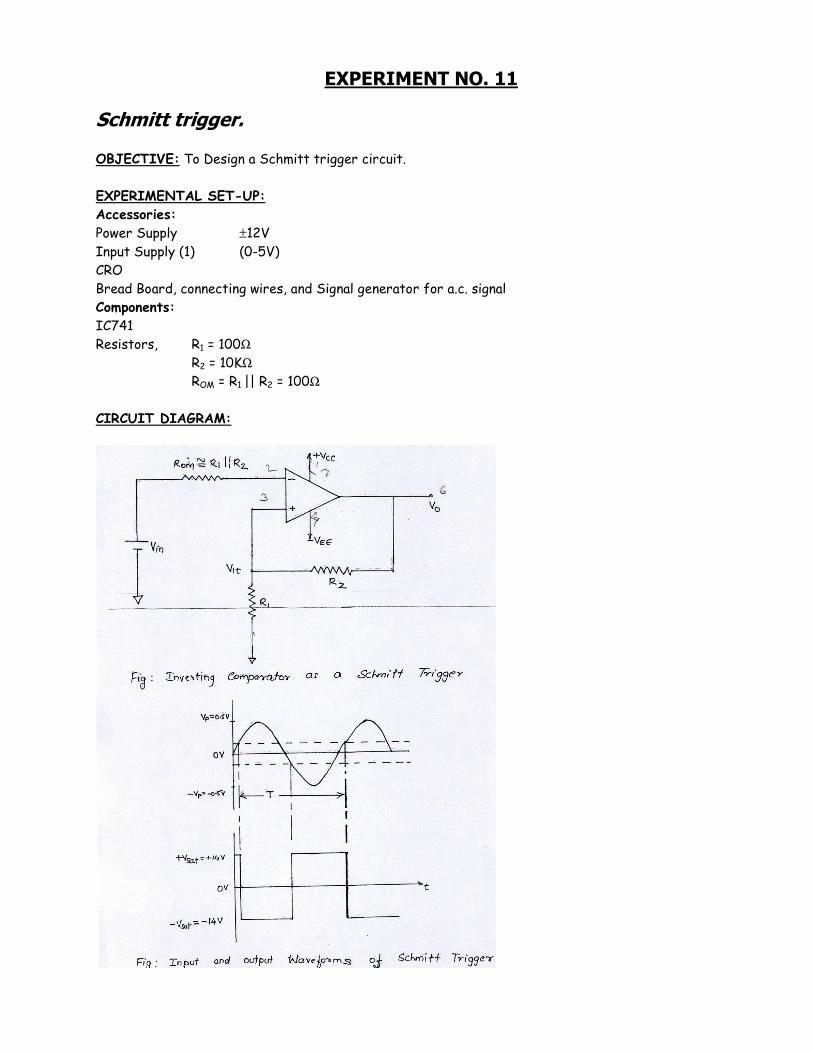
EXPERIMENT NO. 11
Schmitt trigger. OBJECTIVE: To Design a Schmitt trigger circuit. EXPERIMENTAL SET-UP:
Accessories:
Power Supply ±12V Input Supply (1) (0-5V) CRO Bread Board, connecting wires, and Signal generator for a.c. signal Components:
IC741 Resistors, R1 = 100Ω R2 = 10KΩ ROM = R1 || R2 = 100Ω CIRCUIT DIAGRAM:

THEORY:
The Schmitt trigger is an inverting comparator with positive feedback. This circuit converts an irregular-shaped waveform to a square wave or pulse. The circuit is known as the Schmitt trigger or squaring circuit. The input voltage Vin triggers (change the state of) the output Vo every time it exceeds certain voltages levels called the upper threshold voltage Vut and lower threshold voltage Vlt, as shown in figure. This threshold voltages are obtained by using the voltage divider R1 – R2, where the voltage across R1 is feedback to the (+) input. The voltage across R1 is a variable reference threshold voltage that depends on the value and polarity of the output voltage Vo. When Vo = +Vsat, the voltage across R1 is called the upper threshold voltage, Vut. The input voltage Vin must be slightly more positive than Vut in order to cause the output Vo to switch from +Vsat to –Vsat. As long as Vin<Vut, Vo is at +Vsat. Using the voltage-divider rule. Vut = . R1 . (+Vsat) R1 + R2 On the other hand, when Vo= –Vsat ,the voltage across R1 is reffered to as lower threshold voltage, Vlt. Vin must be slightly more negative than Vlt in order to cause Vo to switch from –Vsat to +Vsat. In other words, for Vin values greater than Vlt, Vo is at –Vsat. Vlt = . R1 . (–Vsat) R1 + R2
Thus , if the threshold voltages Vut and Vlt are made larger than the input noise voltages, the positive feedback will eliminate the false output transitions. Also the positive feedback, because of its regenerative action, will make Vo switch faster between +Vsat and –Vsat. Resistance ROM ≅ R1|| R2 is used to minimize the offset problems. PROCEDURE:
1. Make the connections as per the circuit diagram. 2. Choose a value of Resistance ROM ≅ R1|| R2. 3. Give a sine wave input using function generator. 4. Take the output on CRO. 5. Note +Vsat and –Vsat. 6. Calculate
Vut = . R1 . (+Vsat) R1 + R2 And Vlt = . R1 . (–Vsat) R1 + R2
OBSERVATION TABLE:
Sr. No.
Vin (Volts)
Vp (i/p)
+Vsat –Vsat Vut Vlt
1. 2. 3. 4.
CONCLUSION:
Thus we have observed the output of the Schmitt trigger as square wave when sine wave input is given.

EXPERIMENT NO. 12 555 as a Monostable Multivibrator. OBJECTIVE: To Design a Monostable Multivibrator using 555 Timer. EXPERIMENTAL SET-UP:
Accessories:
Power Supply +5V CRO Bread Board, connecting wires, Signal generator. Components:
IC555 Resistors, RA, C
C1 = 0.01µF
CIRCUIT DIAGRAM:

THEORY: A monostable multivibrator, often called a one-shot multivibrator, is a Pulse generating circuit in which the duration of the pulse is determined by the RC network connected externally to the 555 timer. In a stable or standby state the output of the circuit is approximately zero or at logic-low level. When an external trigger pulse is applied, the output is forced to go high (≅ Vcc). The time the output remains high is determined by the external RC network connected to the timer. AT the end of the timing interval, the output automatically reverts back to its logic-low stable state. The output remains low until the trigger pulse is again applied. Then the cycle repeats. The monostable circuit has only one stable state (output low), hence the name monostable. Normally, the output of the monostable multivibrator is low. Monostable operation:
According to fig. (b) initially when output is low, that is , the circuit is in a stable state, transistor Q1 is on and the capacitor C is shorted out of the ground. However, upon application of a negative trigger pulse to pin 2, transistor Q1 is turned off, which releases the short circuit across the external capacitor C and drives the output high. The capacitor C now starts charging up toward Vcc through RA. However, when the voltage across the capacitor equals 2/3 Vcc, comparator 1’s output switches from low to high, which in turn drives the output to its low state via the output of the flip-flop. At the same time, the output of the flip-flop turns transistor Q1 ON, and hence capacitor C rapidly discharges through the transistor. The output of the monostable remains low until a trigger pulse is again applied. Then the cycle reprats. Fig.(c) shows the trigger input, output voltage, and capacitor voltage waveform. As shown here, the pulse width of the trigger input must be smaller than the expected pulse width of the output waveform. Also the trigger pulse must be a negative-going input signal with amplitude larger than 1/3 Vcc. The time duration that the output remains high is given by, tp = 1.1RAC seconds
PROCEDURE: 1. Make the connections as per the circuit diagram. 2. Select RA& C according to time duration required. 3. Take the output on CRO. 4. Calculate the practical time period by the waveform on CRO. 5. Calculate the theoretical time period by 1.1RAC. 6. Calculate the frequency of the waveform.
CONCLUSION:
In this way we have designed monostable multivibrator using 555 timer.

EXPERIMENT NO. 13
555 as a Astable Multivibrator. OBJECTIVE: To Design a Astable Multivibrator using 555 Timer. EXPERIMENTAL SET-UP:
Accessories:
Power Supply +5V CRO Bread Board, connecting wires, Signal generator. Components:
IC555 Resistors, RA, RB, C
C1 = 0.01µF
CIRCUIT DIAGRAM:

THEORY: A astable multivibrator, often called a free-running multivibrator, is a rectangular-wave-generating circuit. Unlike the monostable multivibrator this circuit does not require any external triggering to change the state of the output, hence the name free-running. However, the time during which the output is either high or low is determined by the two resistors and a capacitor, which are externally connected to the 555 timer. Astable operation:
According to fig. (a) initially when output is high, capacitor C starts charging toward Vcc through RA and RB. However as soon as voltage across the capacitor equals 2/3 Vcc, comparator 1 triggers the flip-flop, and the output switches low. Now capacitor C stars discharging through RB and transistor Q1. When the voltage across C equals 1/3 Vcc, comparator 2’s output triggers the flip-flop, and the output goes high. Then the cycle repeats. The output voltage and capacitor voltage are shown in fig (b).
As shown in this figure, the capacitor is periodically charged and discharged between 2/3 Vcc and 1/3 Vcc, respectively. The time during which the capacitor charge from 1/3 Vcc to 2/3 Vcc is equal to the time the output is high and is given by
tc = 0.69(RA + RB) C ………………..(a) Where RA and RB are in ohms and C is in farads. Similarly, the time during which the capacitor discharges from 2/3Vcc to 1/3Vcc is equal to the time the output is low and is given by
td = 0.69(RA) C ………………..(b) Thus the total period of output waveform is
T = tc + td = 0.69(RA + 2RB) C ………………..(c) Frequency of Oscillation is fo = 1 = . 1.45 . ……………………………..(d)
T (RA + 2RB) C
Duty Cycle:- The duty cycle is the ratio of the time tc during which the output is high to the total time period T. It is generally expressed as a percentage. % duty cycle = tc × 100
T
= (RA + RB) 100 ……………………….(e)
(RA + 2RB)

PROCEDURE: 1. Make the connections as per the circuit diagram. 2. Select RA, RB & C according to time duration required. 3. Take the output on CRO. 4. Calculate the the time the output is high, the time the output is low, Total time period,
frequency and % duty cycle.
CONCLUSION:
In this way we have designed astable multivibrator using 555 timer.