laboratory for electromagnetic and electronic...
TRANSCRIPT

Massachusetts Institute of TechnologyLaboratory for Electromagnetic and Electronic Systems
Architectures, Topologies, and Design Methods for
Miniaturized VHF Power ConvertersDavid J. Perreault
PwrSOC
`08Cork, Ireland Sept. 2008
20 kW Kenotron
Rectifier, Circa 1926(From Principles of Rectifier Circuits, Prince and Vogdes, McGraw Hill 1927)
Server Power Supply, Circa 2006(Manufactured by Synqor)
??Circa 2016
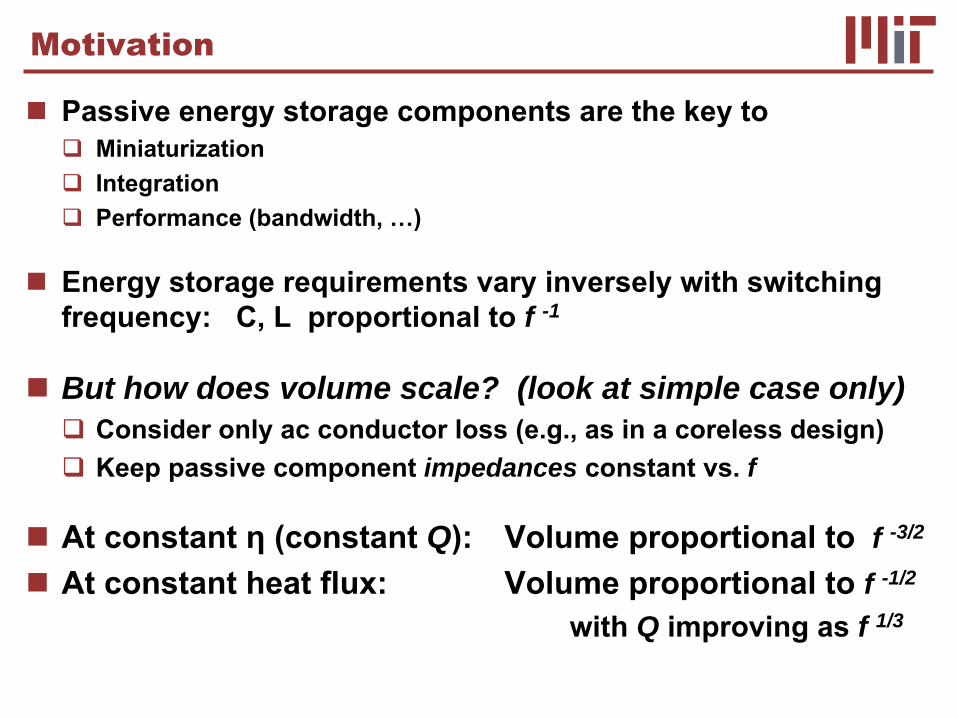
Motivation
Passive energy storage components are the key toMiniaturizationIntegrationPerformance (bandwidth, …)
Energy storage requirements vary inversely with switching frequency: C, L proportional to f -1
But how does volume scale? (look at simple case only)Consider only ac conductor loss (e.g., as in a coreless design)Keep passive component impedances constant vs. f
At constant η (constant Q): Volume proportional to f -3/2
At constant heat flux: Volume proportional to f -1/2
with Q improving as f 1/3

Gating loss (∝
f )
Hard Gating
Switching Frequency Limitations
Loss mechanisms in conventional power electronics limit switching frequency
Core loss in magnetic materials (∝
f k )VSW
(t)ISW
(t)
time
time
p(t)
Switching loss (∝
f )
+−
VIN
RL
L
C
D
M
COSS
VSW
+
-
ISW
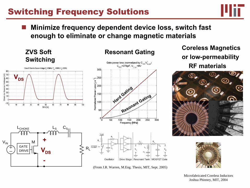
Switching Frequency Solutions
Minimize frequency dependent device loss, switch fast enough to eliminate or change magnetic materials
Hard Gating
Resonant Gating
Resonant GatingZVS Soft Switching
+−
LCHOKE LS CS
RL
VIN MGATEDRIVE VDS
+
-
VDS
VDS
+
-
Coreless Magneticsor low-permeability
RF materials
(From J.R. Warren, M.Eng. Thesis, MIT, Sept. 2005)
Microfabricated Coreless InductorsJoshua Phinney, MIT, 2004

Topology Implications
As frequency increasesDriving high-side switches becomes impracticalControlling commutation among devices becomes challengingTopology must absorb parasitics
device capacitances, interconnect inductance, …
ZVS switching / resonant gating constrain controlDuty ratio and frequency control limitedOnly efficient over a narrow load range
Inverter TransformationStage
Rectifier
System Architecture and Control
Develop system architectures and control strategies that are compatible with VHF conversion
Fixed/narrow duty ratio, frequency rangeMaintain efficient operation across wide load range
Achieved through partitioning of energy conversion and control functions
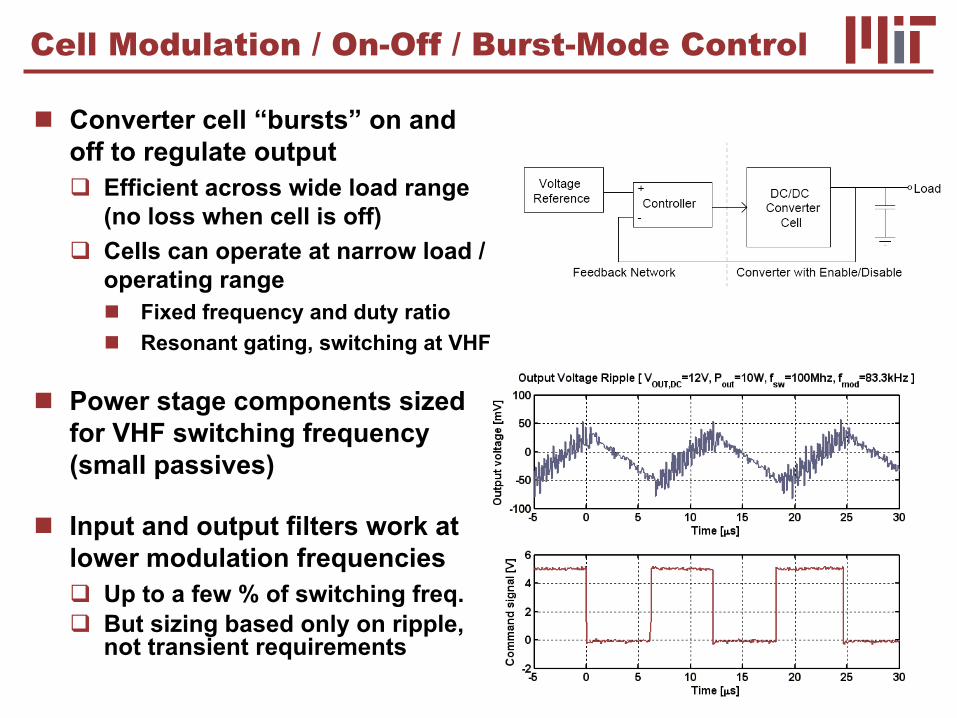
Cell Modulation / On-Off / Burst-Mode Control
Converter cell “bursts” on and off to regulate output
Efficient across wide load range (no loss when cell is off)Cells can operate at narrow load / operating range
Fixed frequency and duty ratioResonant gating, switching at VHF
Power stage components sized for VHF switching frequency (small passives)
Input and output filters work at lower modulation frequencies
Up to a few % of switching freq.But sizing based only on ripple, not transient requirements

Desired Cell Topology Characteristics
Efficient with ZVS switching, resonant gating at VHFSwitch control ports referenced to fixed potentialsAbsorbs device and interconnect parasitics
Compatible with On/Off control at fixed freq., duty ratioAvoid bulk magnetic storage in power stage
Operates well over wide input, output voltage rangesResonant inverter, rectifier characteristics often vary with voltageDesign must accommodate this
Inverter TransformationStage
Rectifier

A maximum frequency thus exists for a specified efficiency
is an important device metric
Uses a large “choke” inductor Reduces performance under on/off control
Inverter performance sensitive to load resistance
Limitations of Traditional Class E Inverter
High device stressesfor Class-E
Tight link between output power, device capacitance, loss, and frequency
INpkds, V3.6V ⋅≈
2DCossout VfCP ⋅⋅∝
fCR%P ossondscond ⋅⋅∝ −
ossonds CR ⋅−

Impedance-Based Waveform Shaping
By controlling the impedance seen at the transistor output, we can shape the voltage waveform
A simple network can null the second harmonic and present a highimpedance at the fundamental and the third harmonic
Impose odd-harmonic symmetry in voltage waveform
This network can be used in an inverter to “shape” the switch voltage to approximate a trapezoidal wave
( )
( ) fsf
ff
fsf
CfL
CC
CfL
22
2
2
151
1615
91
⋅=
=
⋅=
π
π

Class E --> Ф2 Inverter
Class E Inverter
Φ2 Inverter

Ф2 Inverter
Replace dc choke with simple multi-resonant networkNetwork nulls the second harmonic and presents high impedance near the fundamental and the third harmonic Shapes drain-source voltage to reduce peak voltage (25-40%)Reduces sensitivity of ZVS switching to load resistance
Eliminates bulk inductanceSmall inductor sizeFast transient performance
CF is selected as part of the multi-resonant network designEliminates the tie between device capacitance and power that exists in the class E inverter
Vds (idealized)
Rivas, et. al., “A High-Frequency Resonant Inverter Topology with Low Voltage Stress,”
PESC 2007

Example Ф2 Inverter Design
30 MHz class Ф2 inverterVin = 160 – 200 VPout > 320 W @ ηD~ 93%
Breaks class E frequency limitLow device stress
Vds,pk < 2.3 Vin
Small passive componentsFast transient response
LF = 200 nH
L2F = 375 nH
LS = 325 nH
CS = 2 nFC2F = 19 pF
ARF521
0 20 40 60 80 100 120-300
-200
-100
0
100
200
300
400Vds and Vload (VIN=160 V, fs=30 MHz)
Time [ns]
Volta
ge [V
]
Drain VoltageLoad Voltage (VRMS=105.6156 V)
160 170 180 190 200320
340
360
380
400
420
440
460
480
500
520
Input Voltage [V]
Inverter Performance vs. Input Voltage
Out
put P
ower
[W]
160 170 180 190 20090
91
92
93
94
95
Effi
cien
cy [%
]
POUTEfficiency

Resonant Φ2
Boost Converter
Replace inverter load network with resonant rectifierRectifier tuned to replace load network at fundamental
Low peak stress, ground-reference switchFully resonant with small component sizeIdeally suited for constant frequency/duty ratio operation Low energy storage - good candidate for on/off modulation control
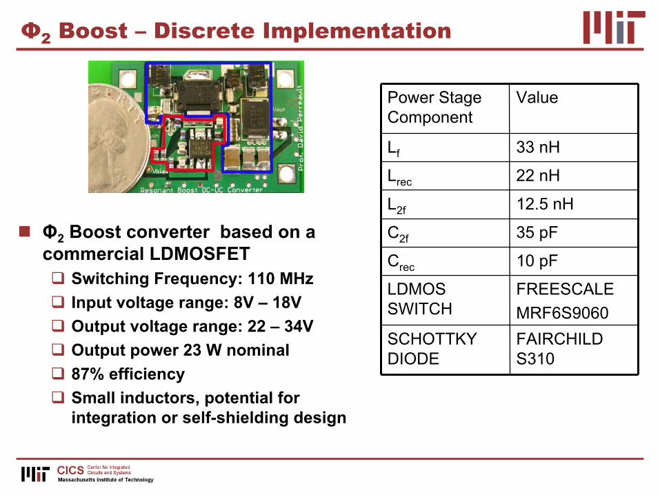
Φ2
Boost –
Discrete Implementation
Φ2 Boost converter based on a commercial LDMOSFET
Switching Frequency: 110 MHzInput voltage range: 8V – 18V Output voltage range: 22 – 34VOutput power 23 W nominal87% efficiencySmall inductors, potential for integration or self-shielding design
FAIRCHILD S310
SCHOTTKY DIODE
FREESCALEMRF6S9060
LDMOS SWITCH
10 pFCrec
35 pFC2f
12.5 nHL2f
22 nHLrec
33 nHLf
ValuePower Stage Component

Closed Loop Efficiency Map
Efficiency ranges from 82% to 87%+ over 5% to 90% load2:1 input voltage range, 1.5:1 output voltage rangeTopology and control contribute to achievable range

Transient Response, 10% to 90% Load
VHF converter transient response excels when compared to equivalent hard-switched boost converter
Hard-switched Boost
Resonant VHF Boost
2.4V, 3mstransient
200 mV, 1ustransient
Summary
Higher frequency offers the potential for Minaturization, Integration, Bandwidth
Switching, gating, and magnetic losses limit the practical operating frequency of conventional designs
Appropriate system design methods enable operation at VHF frequencies
Resonant gating and switchingArchitecture and control
Separate energy conversion, regulationImproved topologiesImproved devices and passive designs also have a big impact
Feasibility of this approach has been demonstratedExample converters at 30-110 MHz at 10’s-100’s of watts, volts
Work in this area is ongoing

StudentsAnthony Sagneri, Yehui
Han, Robert Pilawa, Jackie Hu, Olivia Leitermann, David Jackson, James Warren, Riad
Wahby, Juan Rivas, Joshua Phinney,…
SponsorsMIT Center for Integrated Circuits and Systems National Semiconductor Corp.Texas InstrumentsMIT Consortium on Advanced Automotive SystemsCharles Stark Draper LaboratoryGeneral ElectricDARPANational Science Foundation
Acknowledgments


Research Design Comparison
This general approach appears promisingIncreasingly viable across a range of power levels and applications
105
106
107
10810
-1
100
101
102
103
Frequency (Hz)
Pow
er (W
)Power vs. Frequency for dc-dc Converters
CurrentPractice
(Extracted from C. Xiao, "An Investigationof Fundamental Frequency Limitations forHF/VHF Power Conversion," Ph.D. ThesisCPES, Virginia Tech, July 2006)
Selected Research Designs
Recent MIT Designs
72%
Eff. 78%
Eff. 80%
~70%
80%
Eff ~70-80%
Eff. 91% Eff. 87%
Eff. 87%
Eff. 74%